JP2013211604A5 - - Google Patents
Download PDFInfo
- Publication number
- JP2013211604A5 JP2013211604A5 JP2012078673A JP2012078673A JP2013211604A5 JP 2013211604 A5 JP2013211604 A5 JP 2013211604A5 JP 2012078673 A JP2012078673 A JP 2012078673A JP 2012078673 A JP2012078673 A JP 2012078673A JP 2013211604 A5 JP2013211604 A5 JP 2013211604A5
- Authority
- JP
- Japan
- Prior art keywords
- transducer element
- ultrasonic transducer
- substrate
- element chip
- opening
- Prior art date
- Legal status (The legal status is an assumption and is not a legal conclusion. Google has not performed a legal analysis and makes no representation as to the accuracy of the status listed.)
- Granted
Links
- 239000000758 substrate Substances 0.000 claims description 27
- 230000003014 reinforcing Effects 0.000 claims description 13
- 239000000523 sample Substances 0.000 claims description 10
- 238000005192 partition Methods 0.000 claims description 8
- 238000004519 manufacturing process Methods 0.000 claims 1
- 238000000034 method Methods 0.000 claims 1
- 238000002604 ultrasonography Methods 0.000 claims 1
- 230000005540 biological transmission Effects 0.000 description 6
- 230000000875 corresponding Effects 0.000 description 2
- 238000009423 ventilation Methods 0.000 description 2
- 238000001514 detection method Methods 0.000 description 1
Images
Description
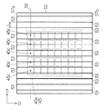
図5に示されるように、開口45は第1方向D1に列を形成する。開口45の輪郭形状の図心45cは第1方向D1の1直線56上で等ピッチに配置される。開口45の輪郭45aは1つの形状の複写で象られることから、同一形状の開口45が一定のピッチで繰り返し配置される。開口45の輪郭45aは例えば四角形に規定される。具体的には矩形に形成される。矩形の長辺は第1方向D1に合わせ込まれる。こうして開口45は矩形の輪郭45aを有することから、仕切り壁51は全長にわたって一定の壁厚みtを有することができる。このとき、仕切り壁51の接合域は長辺の中央位置を含む領域であればよい。特に、仕切り壁51の接合域は長辺の全長を含む領域であればよい。仕切り壁51は長辺の全長にわたって開口45同士の間の全面で補強板52に面接合されることができる。さらに、仕切り壁51の接合域は四角形の各辺に少なくとも1カ所ずつ配置されることができる。仕切り壁51の接合域は四角形を途切れなく囲むことができる。仕切り壁51は四角形の全周にわたって開口45同士の間の全面で補強板52に面接合されることができる。
As shown in FIG. 5, the openings 45 form a row in the first direction D1.
送受信回路62は規定数の切り替えスイッチ64を備える。個々の切り替えスイッチ64はそれぞれ個別に対応の信号線63に接続される。送受信回路62は個々の切り替えスイッチ64ごとに送信経路65および受信経路66を備える。切り替えスイッチ64には送信経路65と受信経路66とが並列に接続される。切り替えスイッチ64はマルチプレクサー61に選択的に送信経路65または受信経路66を接続する。送信経路65にはパルサー67が組み込まれる。パルサー67は振動膜43の共振周波数に応じた周波数でパルス信号を出力する。受信経路66にはアンプ68、ローパスフィルター(LPF)69およびアナログデジタル変換器(ADC)71が組み込まれる。個々の素子23の検出信号は増幅されてデジタル信号に変換される。 The transmission / reception circuit 62 includes a specified number of changeover switches 64. Each changeover switch 64 is individually connected to a corresponding signal line 63. The transmission / reception circuit 62 includes a transmission path 65 and a reception path 66 for each changeover switch 64. A transmission path 65 and a reception path 66 are connected in parallel to the changeover switch 64. The changeover switch 64 selectively connects the transmission path 65 or the reception path 66 to the multiplexer 61. A pulsar 67 is incorporated in the transmission path 65. The pulsar 67 outputs a pulse signal at a frequency corresponding to the resonance frequency of the vibration film 43 . An amplifier 68, a low-pass filter (LPF) 69, and an analog-digital converter (ADC) 71 are incorporated in the reception path 66. The detection signals of the individual elements 23 are amplified and converted into digital signals.
素子チップ17では、行方向に隣接する開口45同士では開口45内の空間は通路58aで相互に連通される。そして、列端の開口45から基板21の輪郭の外側に通路58bは開放される。1本の溝53で通路58a、58bは形成される。こうして1本の溝53で1列の開口45全ての通気は確保されることができる。
In the element chip 17, the openings 45 adjacent to each other in the row direction communicate with each other through a passage 5 8 a. Then, the passage 5 8 b is opened from the opening 45 at the row end to the outside of the outline of the substrate 21. The passages 5 8 a and 5 8 b are formed by one
(5)他の実施形態に係る超音波トランスデューサー素子チップ
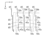
図13は他の実施形態に係る超音波トランスデューサー素子チップ17aを概略的に示す。この素子チップ17aでは1本1本の溝85は局所的に第2方向D2に延びる。こうした局所的な溝85がいくつかの開口45同士の間で通路58a、58bを形成する。複数本の溝85の組み合わせで、基板21の厚み方向からの平面視で1列の開口45を順番に横切って次々に開口45同士を接続する一連の通路58a、58bが形成される。こうして通路58a、58bの組み合わせで1列の開口45全ての通気は確保されることができる。溝85は溝53と同様に構成されることができる。その他の構成は素子チップ17と同様に構成されることができる。図中、素子チップ17と均等な構成や構造には同一の参照符号が付される。
(5) Ultrasonic Transducer Element Chip According to Other Embodiment FIG. 13 schematically shows an ultrasonic transducer element chip 17a according to another embodiment. In the element chip 17a, each
11 電子機器(超音波診断装置)、13 プローブ(超音波プローブ)、13b プローブヘッド、15 表示装置(ディスプレイパネル)、16 筐体、17 超音波トランスデューサー素子チップ、17a 超音波トランスデューサー素子チップ、17b 超音波トランスデューサー素子チップ、21 基板、23 超音波トランスデューサー素子、45 開口、45a 輪郭、52 補強部材(補強板)、53 直線状溝部(溝)、56 平行線、58a 通路、58b 通路、74 処理回路、83 補強部材(補強板用のウエハー)、84 直線状溝部(溝)、85 直線状溝部(溝)、86 直線状溝部(溝)、D1 第1の方向(第1方向)、D2 第2の方向(第2方向)、L (直線状溝部の)間隔、S 開口幅。 DESCRIPTION OF SYMBOLS 11 Electronic device (ultrasonic diagnostic apparatus), 13 Probe (ultrasonic probe), 13b Probe head, 15 Display apparatus (display panel), 16 Housing | casing, 17 Ultrasonic transducer element chip, 17a Ultrasonic transducer element chip, 17b ultrasonic transducer element chip, 21 substrate, 23 ultrasonic transducer element, 45 opening, 45a contour, 52 reinforcing member (reinforcing plate), 53 linear groove (groove), 56 parallel lines, 58a passage, 58b passage, 74 processing circuit, 83 reinforcing member (wafer for reinforcing plate), 84 linear groove (groove), 85 linear groove (groove), 86 linear groove (groove), D1 first direction (first direction), D2 2nd direction (2nd direction), L (space | interval of a linear groove part), S opening width.
Claims (14)
前記基板の第1面に設けられ、前記基板の厚み方向から見た平面視において前記開口と重なる位置に設けられた超音波トランスデューサー素子と、
前記基板の前記第1面とは反対側の前記基板の第2面に設けられた補強部材と、を備え、
前記補強部材は、前記基板の前記第2面と接する面において当該面の面内の第1の方向に並べて配置され、前記開口を含む前記基板の内部空間および前記基板の外部空間を連通する直線状溝部を有し、
前記直線状溝部の間隔が前記第1の方向に沿った前記開口の開口幅よりも小さいことを特徴とする超音波トランスデューサー素子チップ。 A substrate having openings arranged in an array; and
An ultrasonic transducer element provided on the first surface of the substrate and provided at a position overlapping the opening in a plan view as viewed from the thickness direction of the substrate ;
A reinforcing member provided on the second surface of the substrate opposite to the first surface of the substrate;
The reinforcing member is arranged in a first direction within the surface of the substrate on the surface in contact with the second surface of the substrate, and is a straight line that communicates the internal space of the substrate including the opening and the external space of the substrate. Having a groove,
Ultrasonic transducer element chip interval of the linear grooves is characterized and go smaller than the opening width of the opening along the first direction.
前記超音波トランスデューサー素子チップを支持する筐体とを備え、
前記筐体がプローブ本体に着脱可能であることを特徴とするプローブヘッド。 The ultrasonic transducer element chip according to any one of claims 1 to 8,
A housing that supports the ultrasonic transducer element chip ,
Probe head said housing and said detachable der Rukoto to the probe body.
個々の前記開口に超音波トランスデューサー素子が設けられる前記基板の第1面と反対側の前記基板の第2面および前記補強部材の前記表面を重ね合わせる工程と
を含むことを特徴とする超音波トランスデューサー素子チップの製造方法。 Holding a reinforcing member having a surface with linear grooves arranged at intervals smaller than the opening width in the first direction of the openings arranged in an array on the substrate;
Superposing the second surface of the substrate opposite to the first surface of the substrate on which the ultrasonic transducer element is provided in each of the openings, and the surface of the reinforcing member. Manufacturing method of transducer element chip.
前記振動膜に設けられ、前記基板の厚み方向から見た平面視において前記開口と重なる超音波トランスデューサー素子と、 An ultrasonic transducer element provided on the vibration film and overlapping the opening in a plan view as viewed from the thickness direction of the substrate;
前記第2面に設けられ、前記平面視において前記開口を覆う補強部材と、を備え、 A reinforcing member provided on the second surface and covering the opening in the plan view,
前記補強部材は、前記第2面と接する面において第1の方向に並べて配置され、前記開口を含む前記基板の内部空間および前記基板の外部空間を連通する直線状溝部を有し、 The reinforcing member is arranged in a first direction on a surface in contact with the second surface, and has a linear groove portion that communicates the internal space of the substrate including the opening and the external space of the substrate,
前記直線状溝部の間隔が前記第1の方向に沿った前記開口の開口幅よりも小さいことを特徴とする超音波トランスデューサー素子チップ。 The ultrasonic transducer element chip, wherein an interval between the linear grooves is smaller than an opening width of the opening along the first direction.
Priority Applications (7)
| Application Number | Priority Date | Filing Date | Title |
|---|---|---|---|
| JP2012078673A JP5900107B2 (en) | 2012-03-30 | 2012-03-30 | Ultrasonic transducer element chip and probe, electronic device and ultrasonic diagnostic apparatus |
| US13/804,689 US9089872B2 (en) | 2012-03-30 | 2013-03-14 | Ultrasonic transducer element chip, probe, electronic instrument, and ultrasonic diagnostic device |
| TW102110755A TWI599231B (en) | 2012-03-30 | 2013-03-26 | Ultrasonic transducer element chip, probe, electronic instrument, and ultrasonic diagnostic device |
| KR1020147030034A KR101595690B1 (en) | 2012-03-30 | 2013-03-28 | Ultrasonic transducer element chip and probe, and electronic device and ultrasound diagnostic equipment |
| CN201380016075.2A CN104205876B (en) | 2012-03-30 | 2013-03-28 | Ultrasonic transducer element chip, detector, electronic equipment and diagnostic ultrasound equipment |
| PCT/JP2013/002146 WO2013145763A1 (en) | 2012-03-30 | 2013-03-28 | Ultrasonic transducer element chip and probe, and electronic device and ultrasound diagnostic equipment |
| EP13768807.3A EP2833649B1 (en) | 2012-03-30 | 2013-03-28 | Ultrasonic transducer element chip and probe, and electronic device and ultrasound diagnostic equipment |
Applications Claiming Priority (1)
| Application Number | Priority Date | Filing Date | Title |
|---|---|---|---|
| JP2012078673A JP5900107B2 (en) | 2012-03-30 | 2012-03-30 | Ultrasonic transducer element chip and probe, electronic device and ultrasonic diagnostic apparatus |
Related Child Applications (1)
| Application Number | Title | Priority Date | Filing Date |
|---|---|---|---|
| JP2016047228A Division JP6222259B2 (en) | 2016-03-10 | 2016-03-10 | Ultrasonic transducer element chip and probe, electronic device and ultrasonic diagnostic apparatus |
Publications (3)
| Publication Number | Publication Date |
|---|---|
| JP2013211604A JP2013211604A (en) | 2013-10-10 |
| JP2013211604A5 true JP2013211604A5 (en) | 2015-05-14 |
| JP5900107B2 JP5900107B2 (en) | 2016-04-06 |
Family
ID=49234864
Family Applications (1)
| Application Number | Title | Priority Date | Filing Date |
|---|---|---|---|
| JP2012078673A Active JP5900107B2 (en) | 2012-03-30 | 2012-03-30 | Ultrasonic transducer element chip and probe, electronic device and ultrasonic diagnostic apparatus |
Country Status (7)
| Country | Link |
|---|---|
| US (1) | US9089872B2 (en) |
| EP (1) | EP2833649B1 (en) |
| JP (1) | JP5900107B2 (en) |
| KR (1) | KR101595690B1 (en) |
| CN (1) | CN104205876B (en) |
| TW (1) | TWI599231B (en) |
| WO (1) | WO2013145763A1 (en) |
Families Citing this family (14)
| Publication number | Priority date | Publication date | Assignee | Title |
|---|---|---|---|---|
| JP5990930B2 (en) * | 2012-02-24 | 2016-09-14 | セイコーエプソン株式会社 | Ultrasonic transducer element chip and probe, electronic device and ultrasonic diagnostic apparatus |
| JP6102075B2 (en) | 2012-03-30 | 2017-03-29 | セイコーエプソン株式会社 | Ultrasonic transducer element chip and probe, electronic device and ultrasonic diagnostic apparatus |
| JP5900107B2 (en) * | 2012-03-30 | 2016-04-06 | セイコーエプソン株式会社 | Ultrasonic transducer element chip and probe, electronic device and ultrasonic diagnostic apparatus |
| JP6135088B2 (en) | 2012-10-12 | 2017-05-31 | セイコーエプソン株式会社 | Ultrasonic transducer device, probe head, ultrasonic probe, electronic device and ultrasonic diagnostic apparatus |
| JP6175780B2 (en) | 2013-01-28 | 2017-08-09 | セイコーエプソン株式会社 | Ultrasonic device, ultrasonic probe, electronic device and ultrasonic imaging apparatus |
| JP6442821B2 (en) | 2013-09-30 | 2018-12-26 | セイコーエプソン株式会社 | Ultrasonic device and electronic equipment |
| JP6252280B2 (en) * | 2014-03-20 | 2017-12-27 | セイコーエプソン株式会社 | Ultrasonic device unit and probe, electronic apparatus and ultrasonic imaging apparatus |
| JP6402983B2 (en) | 2014-08-29 | 2018-10-10 | セイコーエプソン株式会社 | Ultrasonic device, method for manufacturing ultrasonic device, ultrasonic probe, ultrasonic measuring device, electronic equipment |
| JP6536792B2 (en) * | 2015-03-25 | 2019-07-03 | セイコーエプソン株式会社 | Ultrasonic sensor and method of manufacturing the same |
| JP6625441B2 (en) * | 2015-06-26 | 2019-12-25 | キヤノンメディカルシステムズ株式会社 | Ultrasonic probe |
| JP6597026B2 (en) * | 2015-07-30 | 2019-10-30 | セイコーエプソン株式会社 | Ultrasonic device and ultrasonic module |
| JP6753293B2 (en) * | 2016-12-09 | 2020-09-09 | セイコーエプソン株式会社 | Ultrasonic devices and ultrasonic devices |
| TWI675647B (en) * | 2018-03-08 | 2019-11-01 | 余學致 | Ultrasonic guidance of subacromial bursa |
| JP7205191B2 (en) * | 2018-11-22 | 2023-01-17 | セイコーエプソン株式会社 | Ultrasonic sensors and electronics |
Family Cites Families (22)
| Publication number | Priority date | Publication date | Assignee | Title |
|---|---|---|---|---|
| JPH0765986B2 (en) * | 1986-12-24 | 1995-07-19 | 株式会社東芝 | Array type ultrasonic probe |
| JPH02114947A (en) | 1988-10-24 | 1990-04-27 | Yokogawa Medical Syst Ltd | Preparation of ultrasonic probe |
| JP2002165793A (en) | 2000-11-29 | 2002-06-11 | Olympus Optical Co Ltd | Ultrasonic probe |
| US6758094B2 (en) * | 2001-07-31 | 2004-07-06 | Koninklijke Philips Electronics, N.V. | Ultrasonic transducer wafer having variable acoustic impedance |
| WO2005120130A1 (en) * | 2004-06-03 | 2005-12-15 | Olympus Corporation | Electrostatic capacity type ultrasonic vibrator, manufacturing method thereof, and electrostatic capacity type ultrasonic probe |
| JP4991145B2 (en) * | 2005-11-30 | 2012-08-01 | ブラザー工業株式会社 | Inspection method of piezoelectric actuator |
| JP4618165B2 (en) | 2006-03-06 | 2011-01-26 | 株式会社デンソー | Ultrasonic sensor |
| US7730785B2 (en) * | 2006-04-26 | 2010-06-08 | Denso Corporation | Ultrasonic sensor and manufacture method of the same |
| JP5434109B2 (en) | 2009-02-06 | 2014-03-05 | セイコーエプソン株式会社 | Ultrasonic sensor unit |
| JP5310119B2 (en) | 2009-03-06 | 2013-10-09 | セイコーエプソン株式会社 | Ultrasonic sensor unit |
| US9327316B2 (en) * | 2009-06-30 | 2016-05-03 | Avago Technologies General Ip (Singapore) Pte. Ltd. | Multi-frequency acoustic array |
| JP4947115B2 (en) | 2009-09-30 | 2012-06-06 | 株式会社村田製作所 | Ultrasonic transducer |
| JP2011082624A (en) | 2009-10-02 | 2011-04-21 | Asahi Kasei Electronics Co Ltd | Proximity ultrasonic sensor |
| JP5671876B2 (en) | 2009-11-16 | 2015-02-18 | セイコーエプソン株式会社 | Ultrasonic transducer, ultrasonic sensor, method for manufacturing ultrasonic transducer, and method for manufacturing ultrasonic sensor |
| JP5659564B2 (en) * | 2010-06-10 | 2015-01-28 | コニカミノルタ株式会社 | Ultrasonic probe and ultrasonic diagnostic apparatus |
| JP5695350B2 (en) * | 2010-06-10 | 2015-04-01 | 国立大学法人東北大学 | High frequency vibration piezoelectric element, ultrasonic sensor, and method of manufacturing high frequency vibration piezoelectric element |
| JP5990930B2 (en) * | 2012-02-24 | 2016-09-14 | セイコーエプソン株式会社 | Ultrasonic transducer element chip and probe, electronic device and ultrasonic diagnostic apparatus |
| JP5900107B2 (en) * | 2012-03-30 | 2016-04-06 | セイコーエプソン株式会社 | Ultrasonic transducer element chip and probe, electronic device and ultrasonic diagnostic apparatus |
| JP6019671B2 (en) * | 2012-03-30 | 2016-11-02 | セイコーエプソン株式会社 | Ultrasonic probe, electronic device, and ultrasonic diagnostic apparatus |
| JP6102075B2 (en) * | 2012-03-30 | 2017-03-29 | セイコーエプソン株式会社 | Ultrasonic transducer element chip and probe, electronic device and ultrasonic diagnostic apparatus |
| JP6135088B2 (en) * | 2012-10-12 | 2017-05-31 | セイコーエプソン株式会社 | Ultrasonic transducer device, probe head, ultrasonic probe, electronic device and ultrasonic diagnostic apparatus |
| EP3741042A4 (en) | 2018-02-09 | 2021-01-20 | Huawei Technologies Co., Ltd. | System and method for periodic beam failure measurements |
-
2012
- 2012-03-30 JP JP2012078673A patent/JP5900107B2/en active Active
-
2013
- 2013-03-14 US US13/804,689 patent/US9089872B2/en active Active
- 2013-03-26 TW TW102110755A patent/TWI599231B/en active
- 2013-03-28 EP EP13768807.3A patent/EP2833649B1/en active Active
- 2013-03-28 CN CN201380016075.2A patent/CN104205876B/en active Active
- 2013-03-28 WO PCT/JP2013/002146 patent/WO2013145763A1/en active Application Filing
- 2013-03-28 KR KR1020147030034A patent/KR101595690B1/en active IP Right Grant
Similar Documents
| Publication | Publication Date | Title |
|---|---|---|
| JP2013211604A5 (en) | ||
| JP2013208148A5 (en) | ||
| US10040098B2 (en) | Ultrasonic transducer element chip, probe, electronic instrument, and ultrasonic diagnostic device | |
| JP5754145B2 (en) | Ultrasonic sensors and electronics | |
| US9089872B2 (en) | Ultrasonic transducer element chip, probe, electronic instrument, and ultrasonic diagnostic device | |
| JP2013175879A5 (en) | ||
| JP5990930B2 (en) | Ultrasonic transducer element chip and probe, electronic device and ultrasonic diagnostic apparatus | |
| US9468419B2 (en) | Ultrasonic transducer element unit, probe, probe head, electronic device, and ultrasonic diagnostic device | |
| US10424720B2 (en) | Piezoelectric device, piezoelectric module, and electronic apparatus | |
| US20130223192A1 (en) | Ultrasonic transducer device, probe, electronic instrument, and ultrasonic diagnostic device | |
| JP6623596B2 (en) | Ultrasonic device, ultrasonic module, electronic device, and ultrasonic measuring device | |
| US9782150B2 (en) | Ultrasonic transducer device, probe, electronic instrument, and ultrasonic diagnostic device | |
| JP2015097733A (en) | Ultrasound device and method of producing the same and electronic apparatus and ultrasonic image device | |
| JP2015066202A (en) | Ultrasound device, probe, electronic apparatus and ultrasonic image device | |
| US9233396B2 (en) | Micromachined ultrasonic transducer array | |
| US11378670B2 (en) | Ultrasonic device and ultrasonic apparatus | |
| JP2015177998A (en) | Ultrasonic sensor and electronic apparatus | |
| JP2014198197A (en) | Acoustic matching body, ultrasonic probe, and ultrasonic imaging device | |
| KR101493670B1 (en) | Ultrasonic porbe, ultrasonic probe module having the same, and ultrasonic porbe apparatus having the ultrasonc probe module | |
| JP2016032572A (en) | Manufacturing method of acoustic coupling member | |
| JP2015160104A (en) | Ultrasonic device unit, probe, electronic device and ultrasonic image apparatus | |
| JP2015100093A (en) | Ultrasonic device and probe, and electronic apparatus and ultrasonic image device | |
| JP6221679B2 (en) | Ultrasonic device and probe, electronic apparatus and ultrasonic imaging apparatus | |
| JP6222259B2 (en) | Ultrasonic transducer element chip and probe, electronic device and ultrasonic diagnostic apparatus | |
| JP2017000792A (en) | Ultrasonic transducer element chip, probe, electronic device, and ultrasonic diagnostic device |