JP2013205326A - Manufacturing method of vibration piece, vibration piece, oscillator, electronic components and electronic apparatus - Google Patents
Manufacturing method of vibration piece, vibration piece, oscillator, electronic components and electronic apparatus Download PDFInfo
- Publication number
- JP2013205326A JP2013205326A JP2012076459A JP2012076459A JP2013205326A JP 2013205326 A JP2013205326 A JP 2013205326A JP 2012076459 A JP2012076459 A JP 2012076459A JP 2012076459 A JP2012076459 A JP 2012076459A JP 2013205326 A JP2013205326 A JP 2013205326A
- Authority
- JP
- Japan
- Prior art keywords
- main surface
- electrode
- resonator element
- detection
- arm
- Prior art date
- Legal status (The legal status is an assumption and is not a legal conclusion. Google has not performed a legal analysis and makes no representation as to the accuracy of the status listed.)
- Withdrawn
Links
Images


Abstract
Description
本発明は、振動片の製造方法、振動片、及びこの振動片を用いた振動子、電子部品、電子機器に関する。 The present invention relates to a method for manufacturing a vibrating piece, a vibrating piece, and a vibrator, an electronic component, and an electronic device using the vibrating piece.
従来、基部から延設される振動腕を有し、この振動腕の主平面と側面に電極が設けられた振動片において、振動片の外形形状をウェットエッチングによって成形し、主平面と側面とに設けられる電極を、斜め露光によって形成する製造方法が知られている(例えば、特許文献1、特許文献2参照)。 Conventionally, in a vibrating piece having a vibrating arm extending from the base, and electrodes are provided on the main plane and side of the vibrating arm, the outer shape of the vibrating piece is formed by wet etching, and the main plane and side are formed. A manufacturing method for forming an electrode to be provided by oblique exposure is known (see, for example, Patent Document 1 and Patent Document 2).
上述した特許文献1や特許文献2では、ウェットエッチングを用いて振動片の外形形状を形成しているが、振動片がエッチング異方性を有する材質の場合、エッチング面(側面)において異なった角度の傾斜面が形成されることがあり、その結果、不要振動が発生しやすくなる。従って、不要振動を抑制するために、側面を主平面に対して垂直に近い傾斜角度に近づけるため、オーバーエッチングを行わなければならず、高精度な形状形成は容易ではない。
In Patent Document 1 and
また、電極形成は、斜め露光によって行っているが、側面電極を形成する際、主平面に設けられる平面電極では斜め方向からの光の回り込みによって電極幅が狭くなり、断線される恐れがある。このような場合には、平面電極と側面電極とを別工程で形成しなくてはならない。
また、ウェットエッチングによる外形形成では、各エッチング面の傾斜角度が無視できないほどに差が出る場合があり、斜め露光では、その傾斜角度の差によって側面電極のパターン精度が低下してしまうという課題がある。
In addition, the electrodes are formed by oblique exposure. However, when the side electrodes are formed, the planar electrode provided on the main plane has a risk that the electrode width becomes narrow due to the wraparound of light from the oblique direction, and the electrode is broken. In such a case, the planar electrode and the side electrode must be formed in separate steps.
In addition, in the external shape formation by wet etching, there may be a difference that the inclination angle of each etching surface cannot be ignored, and in the oblique exposure, there is a problem that the pattern accuracy of the side electrode is lowered due to the difference in the inclination angle. is there.
本発明は、上述の課題の少なくとも一部を解決するためになされたものであり、以下の形態または適用例として実現することが可能である。 SUMMARY An advantage of some aspects of the invention is to solve at least a part of the problems described above, and the invention can be implemented as the following forms or application examples.
[適用例1]本適用例に係る振動片の製造方法は、第1主面と前記第1主面と互いに表裏関係にある第2主面とをつなぐ側面に、電極を有する振動片の製造方法であって、前記側面が、前記第2主面に対して傾斜している傾斜面を形成する工程と、前記傾斜面の表面に電極膜を形成する工程と、前記電極膜の表面にレジスト膜を形成する工程と、前記第1主面に対する垂直露光及び現像によって前記レジスト膜の一部を除去し、前記電極膜の一部を露出させる工程と、露出された前記電極膜の一部を除去して前記電極を形成する工程と、を含むことを特徴とする。 Application Example 1 A method for manufacturing a resonator element according to this application example is the manufacture of a resonator element having an electrode on a side surface that connects a first main surface and a second main surface that are in a reverse relation to each other. A method in which the side surface is inclined with respect to the second main surface; a step of forming an electrode film on the surface of the inclined surface; and a resist on the surface of the electrode film. Forming a film; removing a part of the resist film by vertical exposure and development on the first main surface to expose a part of the electrode film; and exposing a part of the exposed electrode film. And removing to form the electrode.
本適用例によれば、側面に傾斜面を形成し、垂直露光によって不要な金属膜を除去して電極を形成することから、従来技術のように、第1主面に設けられる上部電極(例えば、引き回し電極)と、側面に設けられる電極(例えば、検出電極とGND電極)とを斜め露光で形成する際に光の回り込みによって電極幅が狭くなることがなく、上部電極がある場合には、上部電極と側面電極とを共通の露光工程で形成することができる。 According to this application example, since the inclined surface is formed on the side surface and the unnecessary metal film is removed by vertical exposure to form the electrode, the upper electrode provided on the first main surface (e.g. In the case where the electrode width is not narrowed by the wraparound of light and the electrode provided on the side surface (for example, the detection electrode and the GND electrode) is formed by oblique exposure, and there is an upper electrode, The upper electrode and the side electrode can be formed by a common exposure process.
[適用例2]上記適用例に係る振動片の製造方法において、第2主面に対する前記傾斜面の前記傾斜角度が60度〜89度の範囲であること、が好ましい。 Application Example 2 In the method for manufacturing a resonator element according to the application example, it is preferable that the inclination angle of the inclined surface with respect to the second main surface is in a range of 60 degrees to 89 degrees.
傾斜角度を60度〜89度の範囲にすれば、実使用範囲の振動片の厚み又は傾斜の高さ(例えば、60μm〜200μmの範囲)において垂直露光によって所望の電極幅を有する側面電極を形成することができる。 When the tilt angle is in the range of 60 degrees to 89 degrees, a side electrode having a desired electrode width is formed by vertical exposure at the thickness of the vibrating piece in the actual use range or the height of the tilt (for example, in the range of 60 μm to 200 μm). can do.
[適用例3]上記適用例に係る振動片の製造方法において、前記傾斜面を形成する工程は、ドライエッチングによって行われること、が好ましい。 Application Example 3 In the method of manufacturing a resonator element according to the application example, it is preferable that the step of forming the inclined surface is performed by dry etching.
例えば、第1主面側からドライエッチングを開始すれば、加工位置が深くなるにつれて第1主面側ではリデポジション(再堆積)が発生するこことから第2主面側に向かって加工量が少なくなり、その結果、側面に傾斜面を形成できる。この傾斜面の傾斜角度は、ドライエッチング装置のプラズマ電力、加速電圧、エッチングガス種、圧力、流量、基板温度などで調整することが可能である。
振動片が水晶のようにエッチング異方性がある場合、ウェットエッチングでは、振動片の幅の両側で傾斜角度が大幅に異なる場合があるが、ドライエッチングによれば、この傾斜角度の差を小さく抑えることができ、且つその傾斜角度を任意にコントロールすることができ、振動片の側面電極を高精度に形成することができる。
For example, if dry etching is started from the first main surface side, redeposition (redeposition) occurs on the first main surface side as the processing position becomes deeper, so that the processing amount increases toward the second main surface side. As a result, an inclined surface can be formed on the side surface. The inclination angle of the inclined surface can be adjusted by the plasma power, acceleration voltage, etching gas type, pressure, flow rate, substrate temperature, etc. of the dry etching apparatus.
When the resonator element has etching anisotropy such as crystal, wet etching may cause the inclination angle to differ significantly on both sides of the width of the resonator element, but dry etching reduces the difference in inclination angle. The inclination angle can be arbitrarily controlled, and the side electrode of the resonator element can be formed with high accuracy.
[適用例4]上記適用例に係る振動片の製造方法において、前記傾斜面形成する工程は、前記第1主面側及び前記第2主面側からの両面ドライエッチングによって行われること、が好ましい。 Application Example 4 In the method for manufacturing a resonator element according to the application example, it is preferable that the step of forming the inclined surface is performed by double-sided dry etching from the first main surface side and the second main surface side. .
両面ドライエッチングによれば、第1主面と第2主面との中間位置に最大幅がある傾斜面を形成することができる。従って、第1主面側の傾斜面と第2主面側の傾斜面とに、垂直露光によって側面電極を形成することができる。なお、第1主面に上部電極がある場合、第2主面側に下部電極がある場合においても、両面側からの垂直露光によって、上部電極と下部電極と側面電極とを同じ工程で形成することが可能となる。 According to double-sided dry etching, it is possible to form an inclined surface having a maximum width at an intermediate position between the first main surface and the second main surface. Accordingly, side electrodes can be formed on the inclined surface on the first main surface side and the inclined surface on the second main surface side by vertical exposure. Even when the upper electrode is on the first main surface and the lower electrode is on the second main surface side, the upper electrode, the lower electrode, and the side electrode are formed in the same process by vertical exposure from both surfaces. It becomes possible.
[適用例5]上記適用例に係る振動片の製造方法において、前記傾斜面を形成する工程は、前記側面に段部を形成する工程を含むこと、が好ましい。
このように形成された断面形状は、例えば、段部により第2主面側より第1主面側の幅が狭くなるような段付形状となる。
Application Example 5 In the method for manufacturing a resonator element according to the application example, it is preferable that the step of forming the inclined surface includes a step of forming a step portion on the side surface.
The cross-sectional shape thus formed is, for example, a stepped shape in which the width on the first main surface side is narrower than the second main surface side due to the step portion.
このような製造方法では、振動片の外形形状を形成する工程と、振動片に段部を形成する工程と、を有する。例えば、第2主面から段部に至る外形側面と、段部から第1主面に至る段部側面に傾斜面を形成すれば、垂直露光によって外形側面と段部側面の両方に側面電極を形成することができる。 Such a manufacturing method includes a step of forming the outer shape of the resonator element and a step of forming a step portion on the resonator element. For example, if an inclined surface is formed on the outer side surface from the second main surface to the stepped portion and the stepped side surface from the stepped portion to the first main surface, side electrodes are formed on both the outer side surface and the stepped portion side surface by vertical exposure. Can be formed.
[適用例6]上記適用例に係る振動片の製造方法において、前記傾斜面を形成する工程は、前記第1主面側または前記第2主面側または両方に溝を形成する工程を含むこと、が好ましい。 Application Example 6 In the method of manufacturing a resonator element according to the application example, the step of forming the inclined surface includes a step of forming a groove on the first main surface side, the second main surface side, or both. Are preferred.
このような製造方法では、振動片の外形形状をドライエッチングにより形成する工程と、第1主面または第2主面にドライエッチングにより溝を形成する工程と、を有する。従って、この溝の内壁にも傾斜面を形成することができることから、垂直露光によって外形側面と溝の内壁面との両方に側面電極を形成することができる。 Such a manufacturing method includes a step of forming the outer shape of the resonator element by dry etching and a step of forming a groove by dry etching on the first main surface or the second main surface. Therefore, since the inclined surface can be formed also on the inner wall of the groove, the side electrode can be formed on both the outer side surface and the inner wall surface of the groove by vertical exposure.
[適用例7]本適用例に係る振動片は、第1主面と、前記第1主面と互いに表裏関係にある第2主面と、前記第2主面に対して傾斜しており、前記第1主面と前記第2主面とをつなぐ傾斜面と、前記傾斜面に設けられている電極と、を備えていることを特徴とする。 [Application Example 7] The resonator element according to this application example is inclined with respect to the first main surface, the second main surface that is in front-to-back relation with the first main surface, and the second main surface. It is provided with the inclined surface which connects the said 1st main surface and the said 2nd main surface, and the electrode provided in the said inclined surface.
本適用例によれば、前述した適用例に記載の効果を奏する振動片を形成することができる。また、傾斜面に形成する側面電極を複数に分割可能であり、電極配線の設計自由度が増すという効果がある。
また、ドライエッチングによって外形形状を形成すれば、振動腕の両側側面の傾斜角度の差が小さくなり、不要振動の発生を抑制することができる。その結果、高精度、高安定性を有する振動片を実現できる。
According to this application example, it is possible to form a resonator element having the effects described in the application example described above. In addition, the side electrode formed on the inclined surface can be divided into a plurality of parts, which has the effect of increasing the degree of freedom in designing the electrode wiring.
Further, if the outer shape is formed by dry etching, the difference in the inclination angle between the side surfaces of the vibrating arm is reduced, and the occurrence of unnecessary vibration can be suppressed. As a result, a resonator element having high accuracy and high stability can be realized.
[適用例8]上記適用例に係る振動片において、前記第2主面に対する前記傾斜面の傾斜角度が60度〜89度の範囲であること、が好ましい。 Application Example 8 In the resonator element according to the application example described above, it is preferable that an inclination angle of the inclined surface with respect to the second main surface is in a range of 60 degrees to 89 degrees.
傾斜角度を60度〜89度の範囲にすることによって、光の回りこみを抑えて側面電極を精度良く形成することができる。 By setting the inclination angle in the range of 60 degrees to 89 degrees, it is possible to form the side electrodes with high accuracy while suppressing the wraparound of light.
[適用例9]本適用例に係る振動子は、上記適用例に記載の振動片が、パッケージに収容されていること、を特徴とする。 Application Example 9 A vibrator according to this application example is characterized in that the resonator element described in the application example is housed in a package.
本適用例によれば、前述した適用例に記載の効果を有する振動子を実現できる。
また、振動片をパッケージ内に密閉すれば、外部からの水分や塵埃の浸入を防ぎ、振動の安定性を持続させることができる。
According to this application example, it is possible to realize a vibrator having the effects described in the application example described above.
Further, if the resonator element is hermetically sealed in the package, it is possible to prevent moisture and dust from entering from the outside and maintain vibration stability.
[適用例10]本適用例に係る電子部品は、上記適用例に記載の振動片が、回路基板または回路装置に実装されていることを特徴とする。 Application Example 10 An electronic component according to this application example is characterized in that the resonator element described in the application example is mounted on a circuit board or a circuit device.
本適用例によれば、前述した適用例のいずれかに記載の効果を有する回路部品を実現できる。 According to this application example, a circuit component having the effects described in any of the application examples described above can be realized.
[適用例11]本適用例に係る電子機器は、上記適用例に記載の振動片が搭載されていること、を特徴とする。 Application Example 11 An electronic apparatus according to this application example is characterized in that the resonator element described in the application example is mounted.
本適用例によれば、前述した適用例のいずれかに記載の効果を有する電子機器を実現できる。 According to this application example, an electronic device having the effects described in any of the application examples described above can be realized.
以下、本発明の実施形態を図面を参照して説明する。
なお、以下の説明で参照する図は、各部材を認識可能な大きさとするため、各部材ないし部分の縦横の縮尺または膜厚は実際のものとは異なる模式図である。
(実施形態1)
(振動片)
まず、振動片の1例をあげ、図面を参照して構成を説明する。
Hereinafter, embodiments of the present invention will be described with reference to the drawings.
The drawings referred to in the following description are schematic views in which the vertical and horizontal scales or film thicknesses of the respective members or portions are different from actual ones in order to make each member recognizable.
(Embodiment 1)
(Vibration piece)
First, an example of the resonator element will be given and the configuration will be described with reference to the drawings.
図1は、実施形態1に係る振動片の概略構成を示し、(a)は斜視図、(b)は(a)のA−A切断面を示す断面図である。図1に示すように、振動片10は、X軸とX軸に直交するY軸からなる平面に展開され、互いに表裏関係にある第1主面11と第2主面12とを有する。なお、第1主面11及び第2主面12に垂直な軸をZ軸とする。振動片10の材料が水晶の場合、X軸は電気軸、Y軸は機械軸、Z軸は光学軸である。振動片10は、基部20の端部から+Y方向に第1振動腕31と第2振動腕35とが延設され、基部20の他方の端部から−Y方向に第3振動腕40と第4振動腕50とが延設され構成されている。
1A and 1B show a schematic configuration of a resonator element according to the first embodiment. FIG. 1A is a perspective view, and FIG. 1B is a cross-sectional view taken along line AA in FIG. As shown in FIG. 1, the
図1(a)に示すように、基部20と第1振動腕31と第2振動腕35とで音叉形振動片を構成し、基部20と第3振動腕40と第4振動腕50とで音叉形振動片を構成している。この二つの音叉形振動片は基部20で結合されている。このような構成の振動片10をH型振動片と呼ぶことがある。
As shown in FIG. 1A, the
なお、第1振動腕31と第2振動腕35は互いに平行で同じ長さ、同じ断面形状で構成され、第3振動腕40と第4振動腕50は互いに平行で同じ長さ、同じ断面形状で構成されている。本実施例では、第1振動腕31と第2振動腕35とが駆動腕(励振腕)であって、第3振動腕40と第4振動腕50とが検出腕である。よって、以降の説明では、第3振動腕40を第1検出腕40、第4振動腕50を第2検出腕50と表す。
The first vibrating
図示は省略するが、第1振動腕31と第2振動腕35には電極が形成されており、この電極は励振電極(駆動電極)である。また、第1検出腕40と第2検出腕50には電極が形成されており、この電極は検出電極とGND電極である。励振電極は、第1振動腕31と第2振動腕35の表面を介して基部20の第1主面11及び第2主面12に延設され、検出電極とGND電極は第1検出腕40と第2検出腕50の表面を介して基部20の第1主面11及び第2主面12に延設されている。
Although illustration is omitted, electrodes are formed on the first vibrating
このように構成される振動片10は、角速度センサー素子を構成しており、第1振動腕31と第2振動腕35は、それぞれ−X方向と+X方向に変位可能である。そして、励振電極に励振信号(交流信号)を入力することで、第1振動腕31と第2振動腕35とは、±X方向に屈曲振動する。
The
励振信号を入力しているときにY軸(検出軸という)まわりに振動片10を回転させると、第1振動腕31と第2振動腕35との振動方向(面内振動)に対して直角方向にコリオリの力が発生し、このコリオリの力によって第1振動腕31と第2振動腕及び第1検出腕40と第2検出腕50が±Z方向に面外振動する固有振動が励起される。このとき、第1検出腕40と第2検出腕50には圧電効果によって電気軸であるX軸方向に分極が生じる。そして、検出電極に発生する表面電荷量を測定することで、振動片10の角速度を検出することができる。
If the
次に、第1検出腕40及び第2検出腕50の断面形状について説明する。なお、本実施例では、第1振動腕31及び第2振動腕35の断面形状は、第1検出腕40及び第2検出腕50と同じにすることもできるので説明を省略する。また、振動片10における各振動腕及び各検出腕の断面形状は、一つに限らず複数形状が適合可能であるが、図1(b)では、それらの一つを例示して説明する。
図1(b)に示すように、第1検出腕40の−X方向の側面41は傾斜角度θ2の傾斜面からなり、+X方向の側面42は傾斜角度θ1の傾斜面からなる。一方、第2検出腕50の−X方向の側面51は傾斜角度θ2の傾斜面からなり、+X方向の側面52は傾斜角度θ1の傾斜面である。
Next, the cross-sectional shapes of the
As shown in FIG. 1B, the
振動片10の材質が水晶であって、エッチングによって外形形状を形成する場合、製造ばらつきや水晶結晶方位のエッチングレート差によって傾斜角度θ1と傾斜角度θ2は異なる。
さらに、外形形状形成をウェットエッチングで行う場合には、傾斜角度θ1と傾斜角度θ2の差は大きくなる。また、ドライエッチングで行う場合には、傾斜角度θ1と傾斜角度θ2の差はほとんどないか、無視できるほど小さい。
When the vibrating
Further, when the outer shape is formed by wet etching, the difference between the inclination angle θ1 and the inclination angle θ2 becomes large. In the case of dry etching, there is almost no difference between the inclination angle θ1 and the inclination angle θ2, or is negligibly small.
次に、各検出腕に設けられる電極(検出電極)の構成について説明する。
図2は、第1検出腕40と第2検出腕50の電極構成を示し、(a)は実施例1、(b)は実施例2、(c)は実施例3を模式的に示す断面図(図1(a)のA−A切断面)である。
Next, the configuration of electrodes (detection electrodes) provided on each detection arm will be described.
2A and 2B show electrode configurations of the
まず、実施例1について図2(a)を参照して説明する。図示するように、第1検出腕40の側面41には、検出電極62とGND電極63とが形成され、側面42にはGND電極63と検出電極62とが形成されている。また、第1主面11には上部電極としての引き回し電極61が形成されている。
First, Example 1 will be described with reference to FIG. As shown in the drawing, the
一方、第2検出腕50にも同様に、側面51には検出電極62とGND電極63とが形成され、側面52にはGND電極63と検出電極62とが形成されている。また、第1主面11には上部電極としての引き回し電極71が形成されている。
On the other hand, similarly, the
次に、実施例2について図2(b)を参照して説明する。図示するように、第1検出腕40の側面41には、検出電極62とGND電極63とが形成され、側面42にはGND電極63と検出電極62とが形成されている。また、第1主面11には引き回し電極61、第2主面12には引き回し電極66が形成されている。
Next, Example 2 will be described with reference to FIG. As shown in the drawing, the
一方、第2検出腕50にも同様に、側面51には検出電極62とGND電極63とが形成され、側面52にはGND電極63と検出電極62とが形成されている。また、第1主面11には引き回し電極71、第2主面12には引き回し電極72が形成されている。
On the other hand, similarly, the
次に、実施例3について図2(c)を参照して説明する。図示するように、第1検出腕40の側面41には、検出電極62とGND電極63とが形成され、側面42にはGND電極63と検出電極62とが形成されている。
一方、第2検出腕50にも同様に、側面51には検出電極62とGND電極63とが形成され、側面52にはGND電極63と検出電極62とが形成されている。
Next, Example 3 will be described with reference to FIG. As shown in the drawing, the
On the other hand, similarly, the
なお、各実施例において、検出電極62とGND電極63の電極幅は、振動片10の厚みと、隣り合う電極間がショートしない範囲の間隔とから各検出腕に適切に設定される。
なお、上述した各電極は、第1検出腕40及び第2検出腕50のY方向に延設されている。
(振動片の製造方法)
In each embodiment, the electrode widths of the
Each electrode described above extends in the Y direction of the
(Manufacturing method of vibrating piece)
次に、実施形態1に係る振動片10の製造方法について図3、図4を参照して説明する。なお、本実施形態に係る振動片10の製造方法は、前述した実施例1(図2(a)、参照)に示す電極構成の場合について第1検出腕40と第2検出腕50とを例示して説明する。また、本実施形態の製造方法は、単一の水晶ウエハーに複数の振動片10を形成し、振動片10の集合体として一括して製造する製造方法を例示する。なお、製造方法としては、このように集合体による一括製造に限らず、一つの水晶ウエハーに対して一つの振動片10を形成する製造方法でも、適用可能である。
Next, a method for manufacturing the
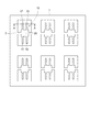
図4は、本実施形態に係る振動片10の製造方法の主要工程を示す断面図、図3は、水晶ウエハーに複数の振動片10を形成する場合を示す平面図である。
まず、図4(a)に示すように、水晶ウエハー1の第1主面11にエッチングマスク80を形成し、複数の振動片10の外形形状を形成する。この際、振動片10は、図3に示すように、水晶ウエハー1に振動片10が複数配置され、基部20と、基部20から延設された第1振動腕31、第2振動腕35、及び第1検出腕40、第2検出腕50とを形成する。この時点では、振動片10は基部20において連結部2で水晶ウエハー1と連結されている。
FIG. 4 is a cross-sectional view showing the main steps of the method for manufacturing the
First, as shown in FIG. 4A, an
エッチングマスク80は、レジスト、またはCr、Au、Niまたはそれらを含んだ金属化合物などの単層、またはそれらの積層膜構造体を用いる。そして、第1主面11側から、ドライエッチングによって振動片10の不要部分を除去し、図3に示すような外形形状を形成する。ドライエッチング工程では、CxFy等のエッチングガスを採用することが望ましい。エッチングガスはドライエッチング装置にてプラズマ・ラジカル化され、反応性ガスとなり、一部はリデポジション(再堆積)の役割を有し、一部はイオンミリングの役割を有する。
For the
第1主面11側からドライエッチングを開始すれば、加工位置が深くなるにつれて加工部分の入口側(第1主面11側)はリデポジション(再堆積)が発生し、第1検出腕40の側面41,42、及び第2検出腕50の側面51,52は、第2主面12側に向かって加工量が減少して、図4(a)に示すような傾斜面が形成される。各傾斜面の第2主面12に対する傾斜角度は、+X方向側ではθ1、−X方向側ではθ2となる。ドライエッチングによれば、θ1≒θ2である。この傾斜面の傾斜角度θ1,θ2は、ドライエッチング装置の加速電圧と電流密度で調整することが可能である。
なお、振動片10の外形形状を形成する工程では、ウェットエッチングを用いることも可能である。
If dry etching is started from the first
Note that wet etching can be used in the step of forming the outer shape of the
次に、図4(b)に示すように、外形形状が形成された振動片10の表面に電極膜90を形成する。電極膜90は、下地層としてCr、上層としてAu層を積層したAu/Cr積層構造体である。電極膜90は、周知の蒸着技術やスパッタ技術等を用いて形成する。
Next, as shown in FIG. 4B, an
次に、図4(c)に示すように、電極膜90の表面にレジスト膜91を形成する。レジスト膜91は、周知のスプレー、スピンコート、ディップや電着法等を用いて形成する。
Next, as illustrated in FIG. 4C, a resist
次に、図4(d)に示すように、露光用マスク81を用いて露光・現像によってレジスト膜91をパターニングする。露光用マスク81にはCr等を用いる。露光は、第1主面11に対して、いわゆる垂直露光を行い、電極膜90の一部を露出させ、開口部を形成する。第2主面12側に形成されたレジスト膜91も除去される。第2主面12側に形成されたレジスト膜91の除去は、第1主面11側からと第2主面12側からの同時露光を行ってもよい。
Next, as shown in FIG. 4D, the resist
続いて、図4(e)に示すように、ドライエッチングまたはウェットエッチングにより前工程で露出された電極膜(不要な電極膜)を除去して電極を形成する。詳述すると、第1検出腕40には、第1主面11に引き回し電極61が形成され、側面41には第1主面側から検出電極62及びGND電極63、側面42には第1主面側からGND電極63及び検出電極62が形成される。一方、第2検出腕50には、第1主面11に引き回し電極71が形成され、側面51には第1主面側から検出電極62及びGND電極63、側面52には第1主面側からGND電極63及び検出電極62が形成される。これらの電極を形成した後、レジスト膜91を除去し、水晶ウエハー1の連結部2を切断して振動片10を個片化する。
Subsequently, as shown in FIG. 4E, the electrode film (unnecessary electrode film) exposed in the previous step is removed by dry etching or wet etching to form an electrode. Specifically, the
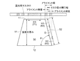
上述した垂直露光によって側面電極が形成可能であることについて、図5、図6を参照して説明する。
図5は、側面電極の形成方法を模式的に図示した説明図である。ここでは、第2検出腕50を例示して説明する。なお、レジスト膜91の図示は省略している。図5に示す露光用マスク81の斜線部分は遮蔽部であり、遮蔽部間の白抜き部分は光透過部(開口部)である。露光用マスク81の遮蔽部は、第1主面11の引き回し電極71とGND電極63の電極幅H1にわたる範囲と、検出電極62の電極幅H2を遮蔽する範囲に形成されている。
The fact that side electrodes can be formed by the vertical exposure described above will be described with reference to FIGS.
FIG. 5 is an explanatory view schematically showing a method of forming side electrodes. Here, the
図5では、GND電極63と検出電極62の形成範囲でアライメントする必要がある範囲がアライメント幅で表されている。また、GND電極63と検出電極62との間の距離Dは、マスク最小開口部幅で律せられる。そして、少なくとも、GND電極63の形成範囲、検出電極62の形成範囲を必ず確保するための範囲以内にアライメント精度を設定する必要がある。また、第1主面11に形成される上部電極71の形成範囲は露光用マスク81の開口部幅H3で表される。
このように構成される露光用マスク81を用いて、側面電極を形成する場合、側面に形成される各電極の幅は、振動片厚み(第2検出腕50の厚み)と傾斜角度によって律せられる。そのことを図6を参照して説明する。
In FIG. 5, the range that needs to be aligned in the formation range of the
When forming side electrodes using the
図6は、傾斜角度θ1と、側面電極幅(H1,H2)の関係を示すグラフである。このグラフは、図5に示す関係を基に、傾斜角度θ1の違いによって側面電極幅がどのくらいになるかを計算して求めたものである。横軸に傾斜角度θ1、縦軸に側面電極幅(H1,H2)を表し、振動片厚み(第2検出腕50の厚み)が60μm、70μm、80μm、100μm、150μm、200μmの場合の各側面電極幅の計算値をプロットしている。 FIG. 6 is a graph showing the relationship between the inclination angle θ1 and the side electrode widths (H1, H2). This graph is obtained by calculating how much the side electrode width becomes due to the difference in the inclination angle θ1, based on the relationship shown in FIG. The horizontal axis represents the tilt angle θ1, the vertical axis represents the side electrode width (H1, H2), and each side surface when the vibrating piece thickness (the thickness of the second detection arm 50) is 60 μm, 70 μm, 80 μm, 100 μm, 150 μm, and 200 μm. The calculated electrode width is plotted.
図6に示すように、側面電極幅H1,H2が存在する傾斜角度θ1は、振動片厚みが200μmであれば略89度まで、振動片厚みが100μmであれば略88.2度(θmax)まで、振動片厚みが70μmであれば略87.5度(θmax)まで、振動片厚みが60μmであれば略87度(θmax)までである。また、傾斜角度θ1が小さくなるほど(傾斜が大きくなるほど)、側面電極幅H1,H2は大きくとれることが分かる。しかし、あまりにも傾斜角度が小さくなると素子特性が悪化するため、傾斜角度θ1は60度以上が好ましい。 As shown in FIG. 6, the inclination angle θ1 at which the side electrode widths H1 and H2 exist is approximately 89 degrees when the vibration piece thickness is 200 μm, and approximately 88.2 degrees (θmax) when the vibration piece thickness is 100 μm. Up to about 87.5 degrees (θmax) if the thickness of the vibrating piece is 70 μm, and up to about 87 degrees (θmax) if the thickness of the vibrating piece is 60 μm. It can also be seen that the side electrode widths H1 and H2 can be increased as the inclination angle θ1 decreases (increases the inclination). However, if the tilt angle becomes too small, the device characteristics deteriorate, so the tilt angle θ1 is preferably 60 degrees or more.
ここで、GND電極63及び検出電極62各々の電極幅H1,H2が存在する傾斜最大角度θmaxは、θmax=tan-1{T/(L1+2L2)}で表すことができる。
なお、第2検出腕50の厚みをT、マスク最小開口幅をL1、アライメント精度をL2とする。従って、振動片10の厚みT(但し、T≧10μm)に対する傾斜角度θ1は、60度≦θ1≦θmaxの範囲に設定することが望ましい。
Here, the maximum inclination angle θmax in which the electrode widths H1 and H2 of the
It is assumed that the thickness of the
なお、傾斜角度θ1とθ2の差は、2度以内とすることがより好ましい。これは、第1検出腕40と第2検出腕50の共振周波数が一致しない場合の振動漏れの影響を抑制することが可能な角度差である(なお、チューニングすることも含める)ことからである。
The difference between the tilt angles θ1 and θ2 is more preferably within 2 degrees. This is because it is an angle difference that can suppress the influence of vibration leakage when the resonance frequencies of the
以上説明した振動片10の製造方法によれば、第1検出腕40、及び第2検出腕50の各側面41,42,51,52に傾斜面を形成し、垂直露光によって不要な電極膜90を除去して電極を形成することから、従来技術のように、第1主面11に設けられる上部電極61,71と、各側面41,42,51,51に設けられる検出電極62及びGND電極とを斜め露光で形成する際に光の回り込みによって電極幅が狭くなってしまうことがなく、上部電極と検出電極及びGND電極とを共通の露光工程で形成することができる。
また、側面41,42,51,52に傾斜面を形成して垂直露光する方法では、側面部に厚さ方向に複数に分割された側面電極を形成することが可能で、振動片10の配線の設計自由度が増すという効果もある。
According to the method of manufacturing the
Further, in the method of forming the inclined surfaces on the side surfaces 41, 42, 51, 52 and performing the vertical exposure, it is possible to form side electrodes divided into a plurality of portions in the thickness direction on the side surfaces, and the wiring of the
また、傾斜角度θ1,θ2を60度〜89度の範囲にすれば、実使用範囲の振動片厚み(60μm〜200μmの範囲で選択された振動片厚み)において垂直露光によって所望の側面電極幅を有する側面電極を形成することができる。 Further, if the inclination angles θ1 and θ2 are set in a range of 60 ° to 89 °, a desired side electrode width can be obtained by vertical exposure at a vibration piece thickness in the actual use range (vibration piece thickness selected in a range of 60 μm to 200 μm). A side electrode can be formed.
また、振動片10の第1検出腕40及び第2検出腕50の側面を形成する工程は、ドライエッチングによって行われる。第1主面11側からドライエッチングを開始すれば、加工位置が深くなるにつれて第1主面11側ではリデポジション(再堆積)が発生するこことから第2主面12側に向かって加工量が少なくなり、その結果、側面に傾斜面を形成できる。この傾斜面の傾斜角度θ1,θ2は、ドライエッチング装置のプラズマ電力、加速電圧、エッチングガス種、圧力、流量、基板温度などで調整することが可能である。
振動片10が水晶のようにエッチング異方性がある場合、ドライエッチングにより加工すると、振動片10の+X方向側の傾斜角度θ1と、−X方向側の傾斜角度θ2とが、θ1≒θ2とすることができるので、第1振動腕31及び第2振動腕35幅の両側で側面電極の寸法差を抑えることができる。
また、ドライエッチングによれば、傾斜角度θ1とθ2の差を2度以内の角度差を抑えることができるので、傾斜角度の差によって発生する第1検出腕40と第2検出腕50の共振周波数の不一致による振動漏れの影響を抑制することができる。
Further, the step of forming the side surfaces of the
When the
Further, according to the dry etching, the difference between the inclination angles θ1 and θ2 can be suppressed to an angle difference of 2 degrees or less, so the resonance frequency of the
なお、以上説明した振動片10の製造方法では、実施例1(図2(a)、参照)の電極構成について説明したが、実施例2(図2(b)、参照)や実施例3(図2(c)、参照)にも適用可能である。
実施例2の構成では、第1検出腕40と第2検出腕50の第2主面12側から、垂直露光によって、下部電極66,76を形成することが可能であり、第1主面11側と第2主面12側からの同時露光も可能である。
実施例3の構成では、第1主面11側の露光用マスク81の上部電極61,71に相当する位置に光透過部(開口部)を形成しておけばよい。
In the method for manufacturing the
In the configuration of the second embodiment, the
In the configuration of the third embodiment, a light transmitting portion (opening) may be formed at a position corresponding to the
なお、振動片10の外形形状の形成工程では、第1主面11及び第2主面12の両面からの両面ドライエッチングや、二度のドライエッチングによって、上述した実施形態1とは異なる断面形状を有する振動腕及び検出腕を形成することが可能である。よって、それらの幾つかを実施形態2に例示して説明する。
(実施形態2)
Note that, in the step of forming the outer shape of the
(Embodiment 2)
続いて、実施形態2について、具体的な実施例をあげ説明する。
図7は、実施形態2に係る振動腕の断面形状及び電極構成の実施例を示し、(a)は実施例1、(b)は実施例2、(c)は実施例3を示す断面図である。なお、各実施例では、第2検出腕50を例示している。
まず、実施例1に係る第2検出腕50と、第2検出腕50の電極構成について説明する。
図7(a)に示すように、第2検出腕50には、第1主面11と第2主面12との中間位置に最大幅がある側面56a,56b,57a,57bが形成されている。
Next, the second embodiment will be described with a specific example.
7A and 7B show examples of the cross-sectional shape and electrode configuration of the vibrating arm according to the second embodiment. FIG. 7A is a cross-sectional view showing Example 1, FIG. 7B is Example 2, and FIG. 7C is Example 3. It is. In each embodiment, the
First, the
As shown in FIG. 7A, the
このような断面形状は、振動片10の第1主面11及び第2主面12の両面に、実施形態1と同様なエッチングマスク80を形成し、両面方向からドライエッチングを行うことによって、図示するような第1主面11と第2主面12との中間位置に最大幅がある側面56a,56b,57a,57bを形成できる。
−X方向の側面56a,56bの傾斜角度はθ2、+X方向の側面57a,57bの傾斜角度はθ1となる。
Such a cross-sectional shape is illustrated by forming an
The inclination angle of the side surfaces 56a and 56b in the −X direction is θ2, and the inclination angle of the side surfaces 57a and 57b in the + X direction is θ1.
そして、第1主面11側と第2主面12側とに、実施形態1(図4、参照)と同様に電極膜90とレジスト膜91とを積層形成し、第1主面11側と第2主面12側との露光用マスク81(図4(d)、参照)を配置し、両面からの垂直露光によって、上部電極71、下部電極76、検出電極72,75及びGND電極73,74を形成する。
Then, an
従って、本実施例による構成であっても、第1主面11側の側面56a,57aと第2主面12側の側面56b,57b各々に、両面方向からの垂直露光によって検出電極72,75及びGND電極73,74とを形成することができる。
なお、上部電極71、下部電極76、及び検出電極72,75、GND電極73,74のうち、いずれかが存在しない構成も可能である。
Therefore, even in the configuration according to the present embodiment, the
A configuration in which any one of the
続いて、実施形態2の実施例2について説明する。実施例2は、振動片10の外形形状が、第2検出腕50の側面に、傾斜面を有する段部が設けられていることを特徴とする。
図7(b)に示すように、第2検出腕50には、第1主面11と第2主面12との中間位置に第1主面11側の幅を狭めるような段部58a,58bが形成されており、段部58aから第1主面11までの間に傾斜面を有する段部側面56cが形成され、段部58aから第2主面12までの間に傾斜面を有する外形側面56dが形成されている。一方、段部58bから第1主面11までの間に傾斜面を有する段部側面57cが形成され、段部58bから第2主面12までの間に傾斜面を有する外形側面57dが形成されている。−X方向の段部側面56cと外形側面56dの傾斜角度はθ2、+X方向の段部側面57cと外形側面57dの傾斜角度はθ1となる。
Subsequently, Example 2 of
As shown in FIG. 7B, the
このような断面形状は、まず、ドライエッチングによって、実施形態1(図4(a)、参照)と同様な外形形状(断面形状)を形成し、さらに、第1主面11の幅を狭めるパターンのエッチングマスクを形成し、ハーフドライエッチングによって段部58a,58bを形成することで実現できる。
Such a cross-sectional shape is a pattern in which an outer shape (cross-sectional shape) similar to that of the first embodiment (refer to FIG. 4A) is first formed by dry etching, and the width of the first
そして、実施形態1(図4、参照)と同様に電極膜90とレジスト膜91とを積層形成し、第1主面11側に露光用マスク81を配置し、両面からの垂直露光によって、段部側面56cにかかる検出電極72を形成し、段部側面57cにかかるGND電極74を形成し、外形側面56dにGND電極73を形成し、外形側面57dに検出電極75を形成する。
Then, similarly to the first embodiment (see FIG. 4), the
従って、本実施例のような段部58a,58bがある構成であっても、第1主面11側からの垂直露光によって、側面電極72〜75を形成することができる。
Therefore, even if it has the structure which has the
なお、第1主面11に上部電極を形成しても、第2主面12に下部電極を形成してもよく、検出電極72,75、GND電極73,74のうち、いずれかが存在しない構成も可能である。
また、本実施例では、図7(b)に示す断面形状を、時計回り方向に90度回転させた断面形状、反時計回りに90度回転させた断面形状にも適用可能である。
Note that the upper electrode may be formed on the first
Further, in this embodiment, the cross-sectional shape shown in FIG. 7B can also be applied to a cross-sectional shape rotated 90 degrees clockwise and a cross-sectional shape rotated 90 degrees counterclockwise.
続いて、実施例3について説明する。実施例3の振動片10は、第1検出腕40及び第2検出腕50の第1主面11側に、傾斜面を有する溝が設けられていることを特徴とする。
図7(c)に示すように、第2検出腕50には、第1主面11側に溝79が形成されている。溝79は第1主面に達する傾斜面79a、79bと、底部79cとから構成されている。
Next, Example 3 will be described. The vibrating
As shown in FIG. 7C, the
このような断面形状は、まず、ドライエッチングによって、実施形態1(図4(a)、参照)と同様な断面形状を形成し、さらに、第1主面11に溝79の開口部に相当するパターンのエッチングマスクを形成し、溝79の底部79cに達するハーフドライエッチングによって傾斜面79a、79bを有する溝79を形成する。+X方向の側面57と傾斜面79aの傾斜角度はθ1、−X方向の側面56と傾斜面79bの傾斜角度はθ2となる。
Such a cross-sectional shape first forms a cross-sectional shape similar to that of the first embodiment (see FIG. 4A) by dry etching, and further corresponds to the opening of the
そして、振動片10の表面全体に、実施形態1(図4、参照)と同様に電極膜90とレジスト膜91とを積層形成し、第1主面11側に露光用マスク81を配置し、第1主面11方向からの垂直露光によって、側面56,57のそれぞれに側面電極62,63を形成し、溝79内の傾斜面79a,79bにかかるGND電極70及び検出電極69を形成する。
Then, an
従って、本実施例のような溝79がある構成であっても、第1主面11側からの垂直露光によって、側面56,57に検出電極62及びGND電極63、溝79内の内壁面に検出電極69及びGND電極70を形成することができる。
Therefore, even in the configuration having the
なお、第2主面12に下部電極を形成してもよく、第2主面12側に溝79を設ける、または第1主面11側と第2主面12側の両方に溝79を設ける構成としてもよい。
(振動子)
The lower electrode may be formed on the second
(Vibrator)
続いて、前述した振動片10を備えた振動子について説明する。
図8は、振動子100の概略構成を示す断面図である。振動子100は、前述した実施形態1または実施形態2に記載の振動片10と、振動片10を格納するパッケージ101と、から構成されている。
Next, a vibrator provided with the above-described vibrating
FIG. 8 is a cross-sectional view illustrating a schematic configuration of the
パッケージ101は、パッケージベース102と、シームリング104と、リッド103等から構成されている。パッケージベース102は、振動片10を収納できるように凹部が形成され、その凹部に振動片10を載置する支持台部105が設けられている。
振動片10の基部20(詳しくは第2主面12側表面)には、前述した第1振動腕31、第2振動腕35、及び第1検出腕40、第2検出腕50に前述した方法を用いて形成された各電極に連続した接続端子(図示せず)が配設されている。
本実施形態では、第1振動腕31と第2振動腕35とに形成される電極は励振電極(駆動電極)であり、第1検出腕40と第2検出腕50とに形成される電極は検出電極及びGND電極である。
The
The method described above for the first vibrating
In the present embodiment, the electrodes formed on the first vibrating
支持台部105には、振動片10に設けられる接続端子と接合するための接続パッド(図示せず)が設けられており、接続端子と接続パッドとが接合される。接続パッドは、パッケージベース102内の図示しない配線に接続され、パッケージベース102の外底面に設けられた外部接続端子106,107と接続されている。
そして、振動片10を支持台部105に接合した後、シームリング104を用いてパッケージベース102とリッド103とを接合し、内部を減圧状態で封止する。
なお、パッケージベース102内に、発振回路を備える構成としてもよい。
The
Then, after the
Note that the
上述したように、振動子100は、前述した振動片10を備えていることから、前述した実施形態1及び実施形態2に記載の効果を有する振動子を実現できる。
また、振動片10をパッケージ101内に密閉すれば、外部からの水分や塵埃の浸入を防ぎ、振動の安定性を持続させることができる。
(電子部品)
As described above, since the
Further, if the
(Electronic parts)
続いて、電子部品について説明する。図示は省略するが、電子部品は、前述した振動片10または振動子100が、回路基板や他の回路装置に実装されている。
前述した振動片10が角速度センサーや加速度センサーである場合、手振れ検出回路装置、位置検出装置、傾斜計装置等の物理量検出装置に適用可能である。さらに、センシングデバイスやタイミングデバイスとしても適用可能である。
(電子機器)
Next, the electronic component will be described. Although not shown, the electronic component includes the above-described vibrating
When the vibrating
(Electronics)
続いて、前述した振動片10または振動子100を備えた電子機器について説明する。
図9は、電子機器の一例として示す携帯電話機の斜視図である。携帯電話機1000は表示部1001と、複数の操作ボタン1002と、受話口1003と、送話口1004とを備え、内部回路構成要素のタイミングデバイスなどとして上述した振動片10また振動子100を備えて構成されている。
Next, an electronic device including the above-described vibrating
FIG. 9 is a perspective view of a mobile phone shown as an example of an electronic device. A
なお、本発明を適用した電子機器としては、上述したような携帯電話機1000に限らず、例えば、電子ブック、パーソナルコンピューター、ディジタルスチルカメラ、液晶テレビ、ビデオテープレコーダー、カーナビゲーション装置、電子手帳、電卓、ワードプロセッサー、ワークステーション、テレビ電話、POS端末、タッチパネルを備えた機器などに好適に用いることができる。
The electronic apparatus to which the present invention is applied is not limited to the
本発明は、その要旨を逸脱しない範囲で種々の変更を加えることが可能である。
例えば、上記実施形態では、振動片として水晶を用いた例を説明したが、水晶以外の圧電体材料を用いることができる。例えば、窒化アルミニウム(AlN)や、ニオブ酸リチウム(LiNbO3)、タンタル酸リチウム(LiTaO3)、チタン酸ジルコン酸鉛(PZT)、四ほう酸リチウム(Li2B4O7)、ランガサイト(La3Ga5SiO14)などの酸化物基板や、ガラス基板上に窒化アルミニウムや五酸化タンタル(Ta2O5)などの圧電体材料を積層させて構成された積層圧電基板、あるいは圧電セラミックスなどを用いることができる。
The present invention can be variously modified without departing from the gist thereof.
For example, in the above-described embodiment, an example in which quartz is used as the resonator element has been described. However, a piezoelectric material other than quartz can be used. For example, aluminum nitride (AlN), lithium niobate (LiNbO 3 ), lithium tantalate (LiTaO 3 ), lead zirconate titanate (PZT), lithium tetraborate (Li 2 B 4 O 7 ), langasite (La 3 Ga 5 SiO 14 ), etc., laminated piezoelectric substrates constructed by laminating piezoelectric materials such as aluminum nitride and tantalum pentoxide (Ta 2 O 5 ) on glass substrates, or piezoelectric ceramics Can be used.
また、圧電体材料以外の材料を用いて振動片を形成することができる。例えば、シリコン半導体材料などを用いて振動片を形成することもできる。
また、振動片の振動(駆動)方式は圧電駆動に限らない。圧電基板を用いた圧電駆動型のもの以外に、静電気力を用いた静電駆動型や、磁力を利用したローレンツ駆動型などの振動片においても、本発明の構成およびその効果を発揮させることができる。
また、本発明の振動片は、H型振動片に限らず、音叉型振動片、ダブルT型振動片、等各種振動片にも適用可能である。
In addition, the resonator element can be formed using a material other than the piezoelectric material. For example, the resonator element can be formed using a silicon semiconductor material or the like.
Further, the vibration (drive) method of the resonator element is not limited to piezoelectric drive. In addition to the piezoelectric drive type using the piezoelectric substrate, the configuration and the effect of the present invention can be exhibited also in an electrostatic drive type using an electrostatic force or a Lorenz drive type using a magnetic force. it can.
In addition, the resonator element according to the invention is not limited to the H-shaped resonator element, but can be applied to various resonator elements such as a tuning fork-type resonator element and a double T-shaped resonator element.
10…振動片、11…第1主面、12…第2主面、20…基部、31…第1振動腕、32,33…第1振動腕の側面、35…第2振動腕、40…第1検出腕、41,42…第1検出腕の側面、50…第2検出腕、51,52…第2検出腕の側面、62…検出電極、63…GND電極、61,71…引き回し電極、80…エッチングマスク、81…露光用マスク、90…電極膜、91…レジスト膜。
DESCRIPTION OF
Claims (11)
前記側面が、前記第2主面に対して傾斜している傾斜面を形成する工程と、
前記傾斜面に電極膜を形成する工程と、
前記電極膜にレジスト膜を形成する工程と、
前記第1主面に対する垂直露光及び現像によって前記レジスト膜の一部を除去し、前記電極膜の一部を露出させる工程と、
露出された前記電極膜の一部を除去して前記電極を形成する工程と、
を含むことを特徴とする振動片の製造方法。 A method of manufacturing a resonator element having an electrode on a side surface connecting a first main surface and a second main surface that is in a front-back relationship with the first main surface,
Forming the inclined surface in which the side surface is inclined with respect to the second main surface;
Forming an electrode film on the inclined surface;
Forming a resist film on the electrode film;
Removing a part of the resist film by vertical exposure and development on the first main surface to expose a part of the electrode film;
Removing a part of the exposed electrode film to form the electrode;
A method of manufacturing a resonator element comprising:
を特徴とする請求項1に記載の振動片の製造方法。 An inclination angle of the inclined surface with respect to the second main surface is in a range of 60 degrees to 89 degrees;
The method of manufacturing a resonator element according to claim 1.
を特徴とする請求項1または請求項2に記載の振動片の製造方法。 The step of forming the inclined surface is performed by dry etching;
The method for manufacturing a resonator element according to claim 1, wherein:
前記第1主面側及び前記第2主面側からの両面ドライエッチングによって行われること、
を特徴とする請求項3に記載の振動片の製造方法。 The step of forming the inclined surface includes:
Performed by double-sided dry etching from the first main surface side and the second main surface side,
The method of manufacturing a resonator element according to claim 3.
前記側面に段部を形成する工程を含むこと、
を特徴とする請求項1ないし請求項4のいずれか一項に記載の振動片の製造方法。 The step of forming the inclined surface includes:
Including a step of forming a step on the side surface;
The method for manufacturing a resonator element according to claim 1, wherein:
前記第1主面側及び前記第2主面側の少なくとも一方に溝を形成する工程を含むこと、
を特徴とする請求項1ないし請求項4のいずれか一項に記載の振動片の製造方法。 The step of forming the inclined surface includes:
Including a step of forming a groove in at least one of the first main surface side and the second main surface side;
The method for manufacturing a resonator element according to claim 1, wherein:
前記第1主面と互いに表裏関係にある第2主面と、
前記第2主面に対して傾斜しており、前記第1主面と前記第2主面とをつなぐ傾斜面と、
前記傾斜面に設けられている電極と、
を備えていることを特徴とする振動片。 A first main surface;
A second main surface that is in reverse relation to the first main surface;
An inclined surface that is inclined with respect to the second main surface and connects the first main surface and the second main surface;
An electrode provided on the inclined surface;
A vibrating piece characterized by comprising:
を特徴とする請求項7に記載の振動片。 An inclination angle of the inclined surface with respect to the second main surface is in a range of 60 degrees to 89 degrees;
The resonator element according to claim 7.
を特徴とする振動子。 The resonator element according to claim 7 or 8 is accommodated in a package,
A vibrator characterized by.
を特徴とする電子機器。 The vibration piece according to claim 7 or claim 8 is mounted,
Electronic equipment characterized by
Priority Applications (1)
| Application Number | Priority Date | Filing Date | Title |
|---|---|---|---|
| JP2012076459A JP2013205326A (en) | 2012-03-29 | 2012-03-29 | Manufacturing method of vibration piece, vibration piece, oscillator, electronic components and electronic apparatus |
Applications Claiming Priority (1)
| Application Number | Priority Date | Filing Date | Title |
|---|---|---|---|
| JP2012076459A JP2013205326A (en) | 2012-03-29 | 2012-03-29 | Manufacturing method of vibration piece, vibration piece, oscillator, electronic components and electronic apparatus |
Publications (2)
| Publication Number | Publication Date |
|---|---|
| JP2013205326A true JP2013205326A (en) | 2013-10-07 |
| JP2013205326A5 JP2013205326A5 (en) | 2015-04-30 |
Family
ID=49524535
Family Applications (1)
| Application Number | Title | Priority Date | Filing Date |
|---|---|---|---|
| JP2012076459A Withdrawn JP2013205326A (en) | 2012-03-29 | 2012-03-29 | Manufacturing method of vibration piece, vibration piece, oscillator, electronic components and electronic apparatus |
Country Status (1)
| Country | Link |
|---|---|
| JP (1) | JP2013205326A (en) |
Cited By (2)
| Publication number | Priority date | Publication date | Assignee | Title |
|---|---|---|---|---|
| JP2016085190A (en) * | 2014-10-29 | 2016-05-19 | セイコーエプソン株式会社 | Vibration element, manufacturing method of the same, electronic device, electronic apparatus and movable body |
| CN110944132A (en) * | 2019-11-20 | 2020-03-31 | 西安微城信息科技有限公司 | Anti-tilt television and using method thereof |
Citations (5)
| Publication number | Priority date | Publication date | Assignee | Title |
|---|---|---|---|---|
| WO2004015370A1 (en) * | 2002-08-07 | 2004-02-19 | Matsushita Electric Industrial Co., Ltd. | Angular-velocity sensor |
| JP2004093318A (en) * | 2002-08-30 | 2004-03-25 | Matsushita Electric Ind Co Ltd | Angular velocity sensor |
| JP2005134364A (en) * | 2003-10-10 | 2005-05-26 | Nippon Dempa Kogyo Co Ltd | Tuning fork type quartz oscillator for angular velocity sensor, and manufacturing method therefor |
| JP2010060361A (en) * | 2008-09-02 | 2010-03-18 | Murata Mfg Co Ltd | Tuning fork-type vibrator, manufacturing method of tuning fork-type vibrator, and angular velocity sensor |
| JP2010154513A (en) * | 2008-11-25 | 2010-07-08 | Citizen Holdings Co Ltd | Method of manufacturing quartz oscillator |
-
2012
- 2012-03-29 JP JP2012076459A patent/JP2013205326A/en not_active Withdrawn
Patent Citations (5)
| Publication number | Priority date | Publication date | Assignee | Title |
|---|---|---|---|---|
| WO2004015370A1 (en) * | 2002-08-07 | 2004-02-19 | Matsushita Electric Industrial Co., Ltd. | Angular-velocity sensor |
| JP2004093318A (en) * | 2002-08-30 | 2004-03-25 | Matsushita Electric Ind Co Ltd | Angular velocity sensor |
| JP2005134364A (en) * | 2003-10-10 | 2005-05-26 | Nippon Dempa Kogyo Co Ltd | Tuning fork type quartz oscillator for angular velocity sensor, and manufacturing method therefor |
| JP2010060361A (en) * | 2008-09-02 | 2010-03-18 | Murata Mfg Co Ltd | Tuning fork-type vibrator, manufacturing method of tuning fork-type vibrator, and angular velocity sensor |
| JP2010154513A (en) * | 2008-11-25 | 2010-07-08 | Citizen Holdings Co Ltd | Method of manufacturing quartz oscillator |
Cited By (4)
| Publication number | Priority date | Publication date | Assignee | Title |
|---|---|---|---|---|
| JP2016085190A (en) * | 2014-10-29 | 2016-05-19 | セイコーエプソン株式会社 | Vibration element, manufacturing method of the same, electronic device, electronic apparatus and movable body |
| US10079590B2 (en) | 2014-10-29 | 2018-09-18 | Seiko Epson Corporation | Vibrator element, electronic device, electronic apparatus, moving object, and method of manufacturing vibrator element |
| CN110944132A (en) * | 2019-11-20 | 2020-03-31 | 西安微城信息科技有限公司 | Anti-tilt television and using method thereof |
| CN110944132B (en) * | 2019-11-20 | 2021-12-21 | 西安微城信息科技有限公司 | Anti-tilt television and using method thereof |
Similar Documents
| Publication | Publication Date | Title |
|---|---|---|
| JP4001029B2 (en) | Tuning fork type piezoelectric vibrating piece, method for manufacturing the same, and piezoelectric device | |
| US9222775B2 (en) | Vibrator element, sensor unit, and electronic device | |
| JP5991464B2 (en) | Vibrating piece and manufacturing method thereof, vibrating element, vibrator, electronic device, and electronic apparatus | |
| US8640540B2 (en) | Vibrating element, vibrator, and electronic apparatus | |
| JP6078968B2 (en) | Manufacturing method of vibrating piece | |
| US20130193807A1 (en) | Quartz crystal vibrating piece and quartz crystal device | |
| US9013093B2 (en) | Vibrating reed, electronic device, and electronic apparatus | |
| JP5765087B2 (en) | Bending vibration piece, method for manufacturing the same, and electronic device | |
| JP5967354B2 (en) | Vibrating piece and manufacturing method thereof, vibrating element, vibrator, electronic device, and electronic apparatus | |
| JP2013024721A (en) | Vibration gyro element, gyro sensor and electronic apparatus | |
| US9140549B2 (en) | Physical quantity detection element, physical quantity detection device, and electronic apparatus | |
| JP2013205328A (en) | Vibration piece, sensor unit and electronic apparatus | |
| JP5970690B2 (en) | SENSOR ELEMENT, SENSOR UNIT, ELECTRONIC DEVICE, AND SENSOR UNIT MANUFACTURING METHOD | |
| JP2013050321A (en) | Physical quantity detector and electronic apparatus | |
| JP2013186029A (en) | Vibration piece, sensor unit, and electronic apparatus | |
| JP2012257141A (en) | Crystal vibrating piece, gyro sensor, electronic apparatus and manufacturing method of crystal vibrating piece | |
| JP3941736B2 (en) | Quartz vibrating piece, manufacturing method thereof, quartz crystal device using quartz crystal vibrating piece, mobile phone device using quartz crystal device, and electronic apparatus using quartz crystal device | |
| JP2008224627A (en) | Angular velocity sensor, method of manufacturing the same, and electronic apparatus | |
| JP2013207332A (en) | Manufacturing method of vibration piece | |
| JP2013205326A (en) | Manufacturing method of vibration piece, vibration piece, oscillator, electronic components and electronic apparatus | |
| JP6210345B2 (en) | Gyro sensor element, gyro sensor unit, electronic device, and manufacturing method of gyro sensor unit | |
| JP5716557B2 (en) | Vibrating piece, gyro sensor, electronic device, and method of manufacturing the vibrating piece | |
| JP2017207283A (en) | Manufacturing method for vibration element | |
| JP6551649B2 (en) | Method of manufacturing vibrating piece, vibrating piece, vibrator, oscillator, real time clock, electronic device, and moving body | |
| JP2013234873A (en) | Vibrating piece and manufacturing method for the vibrating piece, gyro sensor, and electronic apparatus and mobile body |
Legal Events
| Date | Code | Title | Description |
|---|---|---|---|
| RD04 | Notification of resignation of power of attorney |
Free format text: JAPANESE INTERMEDIATE CODE: A7424 Effective date: 20150107 |
|
| A521 | Request for written amendment filed |
Free format text: JAPANESE INTERMEDIATE CODE: A523 Effective date: 20150316 |
|
| A621 | Written request for application examination |
Free format text: JAPANESE INTERMEDIATE CODE: A621 Effective date: 20150316 |
|
| A977 | Report on retrieval |
Free format text: JAPANESE INTERMEDIATE CODE: A971007 Effective date: 20160217 |
|
| A131 | Notification of reasons for refusal |
Free format text: JAPANESE INTERMEDIATE CODE: A131 Effective date: 20160223 |
|
| A761 | Written withdrawal of application |
Free format text: JAPANESE INTERMEDIATE CODE: A761 Effective date: 20160407 |