JP2013200329A - Microscope system - Google Patents
Microscope system Download PDFInfo
- Publication number
- JP2013200329A JP2013200329A JP2012066820A JP2012066820A JP2013200329A JP 2013200329 A JP2013200329 A JP 2013200329A JP 2012066820 A JP2012066820 A JP 2012066820A JP 2012066820 A JP2012066820 A JP 2012066820A JP 2013200329 A JP2013200329 A JP 2013200329A
- Authority
- JP
- Japan
- Prior art keywords
- light
- unit
- wavelength
- microscope system
- excitation light
- Prior art date
- Legal status (The legal status is an assumption and is not a legal conclusion. Google has not performed a legal analysis and makes no representation as to the accuracy of the status listed.)
- Pending
Links
Images


Landscapes
- Investigating, Analyzing Materials By Fluorescence Or Luminescence (AREA)
- Microscoopes, Condenser (AREA)
Abstract
Description
本発明は、顕微鏡システムに関する。 The present invention relates to a microscope system.
走査型顕微鏡と、この走査型顕微鏡で検出された信号光(蛍光)を分光して検出する分光ユニット(分光部)と、を有する顕微鏡システムにおいて、分光ユニットは一般的に信号光を回折格子などの分光素子で分光し、ライン状に並べられたPMT(Photomultiplier Tube:光電子倍増管)などの受光器で検出するように構成されている。このような信号光を検出する走査型顕微鏡と共に用いる分光ユニットでは、標本を励起して信号光(蛍光)を発生させる励起光も信号光に混ざり込むために、この励起光をカットする必要がある。従来の分光ユニットではこのような励起光をカットするために、分光素子で分光された光(分光光)のうち、励起光の波長に対応する光を遮断するための短冊状スリットが設けられていた(例えば、特許文献1参照)。 In a microscope system having a scanning microscope and a spectroscopic unit (spectrometer) for spectrally detecting signal light (fluorescence) detected by the scanning microscope, the spectroscopic unit generally divides the signal light into a diffraction grating, etc. The light is separated by a light receiving element such as PMT (Photomultiplier Tube: photomultiplier tube) arranged in a line. In the spectroscopic unit used with the scanning microscope for detecting such signal light, the excitation light that excites the sample and generates signal light (fluorescence) is also mixed with the signal light. Therefore, it is necessary to cut the excitation light. . In order to cut off such excitation light, the conventional spectroscopic unit is provided with a strip-shaped slit for blocking light corresponding to the wavelength of the excitation light among the light (spectral light) dispersed by the spectroscopic element. (For example, see Patent Document 1).
しかしながら、標本を励起するための励起光の波長を変化させると、励起光の波長の光が受光器に入射する位置も変化するため、短冊状スリットの位置もその波長に対応させて変化させなければならない。そのため、励起光の波長毎に短冊状スリットを用意しなければならず、標本の観察作業が繁雑になるとともに、装置が複雑になるという課題があった。 However, if the wavelength of the excitation light for exciting the sample is changed, the position where the light with the wavelength of the excitation light enters the receiver also changes, so the position of the strip slit must also be changed according to the wavelength. I must. Therefore, a strip-shaped slit has to be prepared for each wavelength of the excitation light, and there is a problem that the observation work of the specimen becomes complicated and the apparatus becomes complicated.
本発明はこのような課題に鑑みてなされたものであり、励起光の波長に合わせて信号光から除去する光の波長を変化させることができる顕微鏡システムを提供することを目的とする。 The present invention has been made in view of such problems, and an object thereof is to provide a microscope system capable of changing the wavelength of light to be removed from signal light in accordance with the wavelength of excitation light.
前記課題を解決するために、本発明に係る顕微鏡システムは、光源から出射された励起光を走査して対物レンズにより標本上に集光し、この標本上からの蛍光を対物レンズで集光する顕微鏡と、顕微鏡からの蛍光を分光する分光素子、及びこの分光素子により分光された分光光を受光する受光器を含む分光部と、を有する顕微鏡システムであって、分光部は、励起光が受光器に向かうことを抑制し、蛍光を受光器に導く波長選択部を有し、この波長選択部を制御して励起光の波長に対応させて波長選択部の波長特性を変化させる制御部を備えることを特徴とする。 In order to solve the above problems, a microscope system according to the present invention scans excitation light emitted from a light source, condenses it on a specimen by an objective lens, and condenses fluorescence from the specimen by the objective lens. A microscope system comprising: a microscope; a spectroscopic element that splits fluorescence from the microscope; and a spectroscopic unit that includes a light receiver that receives spectroscopic light split by the spectroscopic element. The spectroscopic unit receives excitation light. A wavelength selection unit that suppresses the light from going to the detector and guides the fluorescence to the light receiver, and includes a control unit that controls the wavelength selection unit to change the wavelength characteristics of the wavelength selection unit according to the wavelength of the excitation light. It is characterized by that.
このような顕微鏡システムにおいて、波長選択部は、波長特性が異なる2以上の光学素子と、これらの光学素子の各々を分光部の光路に挿抜するフィルタ挿抜部と、を有し、制御部は、フィルタ挿抜部を制御することにより、光学素子の少なくとも一つを光路上に挿入し、その他の光学素子を光路上から抜脱することが好ましい。 In such a microscope system, the wavelength selection unit includes two or more optical elements having different wavelength characteristics, and a filter insertion / extraction unit that inserts / extracts each of these optical elements into / from the optical path of the spectroscopic unit. It is preferable that at least one of the optical elements is inserted into the optical path and the other optical elements are removed from the optical path by controlling the filter insertion / extraction unit.
また、このような顕微鏡システムにおいて、波長選択部は、所定の波長特性を有する光学素子を含み、この光学素子に対する励起光の入射角度を変化させる角度調整部を有し、制御部は、角度調整部を制御することが好ましい。 In such a microscope system, the wavelength selection unit includes an optical element having a predetermined wavelength characteristic, and includes an angle adjustment unit that changes the incident angle of the excitation light with respect to the optical element, and the control unit adjusts the angle. It is preferable to control the part.
また、このような顕微鏡システムは、制御部により制御される角度調整部の入射角度を励起光の波長に対応付けて記憶する記憶部を有し、この記憶部から読み出された入射角度になるように、制御部により角度調整部を制御することが好ましい。 Further, such a microscope system has a storage unit that stores the incident angle of the angle adjusting unit controlled by the control unit in association with the wavelength of the excitation light, and has the incident angle read from the storage unit. Thus, it is preferable to control the angle adjustment unit by the control unit.
また、このような顕微鏡システムにおいて、光学素子は、励起光を反射し、蛍光を透過するノッチフィルタであることが好ましい。 In such a microscope system, the optical element is preferably a notch filter that reflects excitation light and transmits fluorescence.
また、このような顕微鏡システムにおいて、波長選択部は、所定の反射率を有する平面が所定の間隔で対向するように配置された2つの光透過部材と、間隔を変化させる間隔調整部及び光透過部材に対する励起光及び蛍光の入射角度を変化させる角度調整部の少なくとも一方とを含むフィルタユニットを有し、制御部により間隔調整部及び角度調整部の少なくとも一方を制御することが好ましい。 In such a microscope system, the wavelength selection unit includes two light transmission members arranged so that planes having a predetermined reflectance face each other at a predetermined interval, an interval adjustment unit that changes the interval, and a light transmission unit. It is preferable to have a filter unit including at least one of an angle adjustment unit that changes the incident angle of excitation light and fluorescence to the member, and to control at least one of the interval adjustment unit and the angle adjustment unit by the control unit.
また、このような顕微鏡システムは、制御部により制御される間隔調整部の間隔を励起光の波長に対応づけて記憶する記憶部を有し、この記憶部から読み出された間隔になるように、制御部により間隔調整部を制御することが好ましい。 In addition, such a microscope system has a storage unit that stores the interval of the interval adjustment unit controlled by the control unit in association with the wavelength of the excitation light, so that the interval is read from the storage unit. It is preferable that the interval adjusting unit is controlled by the control unit.
また、このような顕微鏡システムは、制御部により制御される角度調整部の入射角度を励起光の波長に対応づけて記憶する記憶部を有し、この記憶部から読み出された入射角度になるように、制御部により角度調整部を制御することが好ましい。 Further, such a microscope system has a storage unit that stores the incident angle of the angle adjusting unit controlled by the control unit in association with the wavelength of the excitation light, and has the incident angle read from the storage unit. Thus, it is preferable to control the angle adjustment unit by the control unit.
また、このような顕微鏡システムにおいて、光透過部材の平面の反射率は90%以上であることが好ましい。 In such a microscope system, it is preferable that the reflectance of the plane of the light transmitting member is 90% or more.
また、このような顕微鏡システムにおいて、光透過部材の平面の各々には、反射率が異なる少なくとも2以上の領域が形成され、2つの光透過部材は、光軸に直交する面内を移動させて励起光が入射する領域を変化させる位置調整部を有することが好ましい。 In such a microscope system, at least two regions having different reflectivities are formed on each plane of the light transmitting member, and the two light transmitting members are moved in a plane perpendicular to the optical axis. It is preferable to have a position adjusting unit that changes the region where the excitation light is incident.
また、このような顕微鏡システムにおいて、波長選択部は、入射する光のうち、少なくとも蛍光を含む光を反射する第1の光学素子と、第1の光学素子で反射された光のうち、少なくとも蛍光を含む光を反射する第2の光学素子と、を有し、第1の光学素子及び第2の光学素子のうちの少なくとも一方は、フィルタユニットであることが好ましい。 In such a microscope system, the wavelength selection unit includes at least a first optical element that reflects light including at least fluorescence among incident light, and at least fluorescence among light reflected by the first optical element. It is preferable that at least one of the first optical element and the second optical element is a filter unit.
また、このような顕微鏡システムにおいて、第1の光学素子及び第2の光学素子の反射面は、略平行に配置されていることが好ましい。 In such a microscope system, it is preferable that the reflecting surfaces of the first optical element and the second optical element are arranged substantially in parallel.
本発明を以上のように構成すると、励起光の波長に合わせて信号光から除去する光の波長を変化させることができる顕微鏡システムを提供することができる。 When the present invention is configured as described above, it is possible to provide a microscope system that can change the wavelength of light to be removed from signal light in accordance with the wavelength of excitation light.
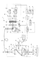
以下、本発明の好ましい実施形態について図面を参照して説明する。まず、図1を用いて分光機能付き走査型顕微鏡の一例である顕微鏡システムの構成を説明する。この顕微鏡システム1は、光源系10、共焦点ユニット20及び顕微鏡30を有する共焦点顕微鏡と、共焦点顕微鏡で集光された信号光(蛍光)を分光して検出する分光部である分光ユニット40と、情報処理装置50と、を有する。この顕微鏡システム1において、共焦点ユニット20と分光ユニット40とは、ファイバカプラ29a,29bを介して光ファイバ28により光学的に接続されている。
Hereinafter, preferred embodiments of the present invention will be described with reference to the drawings. First, the configuration of a microscope system, which is an example of a scanning microscope with a spectral function, will be described with reference to FIG. The
光源系10は、レーザ装置11と、光ファイバ13と、ファイバカプラ12,14と、を有する。レーザ装置11は、例えば、レーザーダイオードを備え、目的の波長特性を有する励起光(照明光)を射出する。この励起光は、光ファイバ13を介して共焦点ユニット20に導かれる。なお、図1の例では、励起光として、標本33を励起して蛍光を発光させるための光を射出する。また、レーザ装置11は、異なる波長の励起光を選択して放射することができるように構成されている。そのため、観察者は、観察する標本に応じてこの標本を励起するための光の波長を選択することができる。
The
共焦点ユニット20は、光源系10からの励起光を略平行光束とするコリメートレンズ21と、ダイクロイックミラー22と、走査ユニット23と、スキャナレンズ24と、集光レンズ25と、ピンホール26aを有するピンホール板26と、リレーレンズ27と、を有する。また、顕微鏡30は、対物レンズ32及び第2対物レンズ31と、標本33が載置されるステージ34と、を有する。これらの共焦点ユニット20と顕微鏡30とを組み合わせて走査型共焦点顕微鏡が構成される。なお、ダイクロイックミラー22は、光源系10から射出されたレーザ光を顕微鏡30側に反射し、このレーザ光により励起した標本33から放射される蛍光を透過するように構成されている。また、集光レンズ25の像側焦点は、ピンホール板26のピンホール26aと略一致するように配置されている。
The
分光ユニット40は、ファイバカプラ29bを介して光ファイバ28から入射する信号光(図1の例では蛍光)を略平行光束とするコリメート光学系41と、異なる分光特性を有する3種の分光素子である回折格子431,432,433(まとめて「回折格子43」とする)と、それらを保持して回転する回転テーブル42と、複数の受光素子45aがアレー状に並べられてラインディテクタを構成する受光器45と、回折格子43(回折格子431〜433のいずれか)から射出された回折光(分光光)を受光器45の受光面に結像させる集光光学系44と、受光器45を駆動するための電源を供給する高圧電源46と、受光器45の各受光素子45aの出力を増幅するとともにディジタル化して検出データとして出力する検出回路47と、を有する。なお、受光素子45aに入射する信号光(分光光)のNAが、この受光素子45aの有効NA又は最適NAの範囲内になるように、前段の光学系(コリメート光学系41や集光光学系44)が形成されている。
The
情報処理装置50は、検出回路47から出力される検出データを記憶するフレームメモリ51と、記憶されている検出データに基づいて目的の分光特性を演算する中央処理ユニット(以下、「CPU」と呼ぶ)52と、表示装置53と、外部記憶装置54と、入力装置55と、スキャナ駆動装置56と、を有する。ここで、CPU52は、図示していないが演算部と主記憶部とを有する。また、表示装置53には、例えば、液晶表示装置が用いられる。また、外部記憶装置54には、例えば、ハードディスク装置、光記録媒体記憶装置、半導体記憶装置等が用いられる。また、入力装置55には、例えば、キーボード、マウス等の機器を含む。
The
外部記憶装置54には、CPU52の動作プログラム及び各種データが記憶される。具体的には、複数個の光学要素のそれぞれについての分光特性(分光データ)を、それぞれの光学要素に対応させて記憶する記憶手段としての機能を有する。このようなプログラム及び予め与えられたデータは、例えば、図示しない読み取り装置を用いてCD−ROM等の記憶媒体から読み出してインストールすることにより、外部記憶装置54に記憶される。
The
CPU52は、外部記憶装置54に記憶されるプログラムをロードして、各種制御、演算処理等を行う。この外部記憶装置54に記憶されるプログラムには、スキャナ駆動装置56を介して走査ユニット23の作動を制御する手段と、測定対象から得られたデータに基づいて分光特性を求める演算を行う手段と、受け付けた光学要素を特定する情報に基づいて記憶手段により記憶される、使用する光学要素についての分光特性情報を読み出して、当該使用する光学系が有する分光特性情報を求め、この分光特性情報と、上述の分光ユニット40から出力される分光データとを用いて対象の分光特性を求める手段と、によりCPU52を動作させるプログラムが含まれる。また、記憶装置と共に、複数個の光学要素のそれぞれについての分光特性を、それぞれの要素対応に記憶する記憶手段として、CPU52を動作させるプログラムも含まれる。さらに、レーザ装置11から放射される励起光の波長を選択して作動させるプログラムや、後述する分光ユニット140,240における波長選択部148,248の作動を制御するプログラムも含まれる。
The
分光ユニット40について、さらに詳細に説明する。この分光ユニット40は、光ファイバ28を介して信号光を取り込み、回折格子431〜433のいずれかにより分光させて、受光器45の各受光素子45aにおいて分光光の受光を行う。
The
図1に示すように、光ファイバ28は、ファイバカプラ29bで分光ユニット40に取り付けられている。光ファイバ28からの信号光は、全ての光束が、コリメート光学系41により略平行光にされ、回折格子431〜433のうち選択された回折格子43に入射される。この回折格子43に入射した信号光は、その波長によって決まる回折角方向に回折されて分光される。そして、分光された信号光は、集光光学系44で集光されて、受光器45の受光面に結像されてこの受光器45に入射される。受光器45からは、各受光素子45aに入射した信号光の光量に対応した電気信号が出力され、情報処理装置50により処理することにより、波長対強度の分光信号を得ることができる。
As shown in FIG. 1, the
なお、回折格子431〜433は、刻線本数(1mm当たりの回折格子溝の本数)が異なる。また、これらの回折格子431〜433は、回転テーブル42上に角度位置を変えて設置されている。そのため、回転テーブル42を回して回折格子431〜433に入射する角度を変えることで、受光器45で検出される波長帯域を変更することができる。また、回折格子431〜433のうち、ある回折格子から他の回折格子に切替えることで、波長分解能を変えることもできる。
The
光ファイバ28は、石英のコアからなるステップインデックス型であり、コア径は50μm、NAは0.22である。この光ファイバ28からファイバカプラ29bを介して射出された光は、分光ユニット40内に導かれる。本実施形態では、コリメート光学系41を介して分光光学系に導かれる。このとき、本実施形態に係る顕微鏡システム1では、微弱な光信号(蛍光)を扱う。このため、高いSN比を得るには、光ファイバ28により導入された信号光束を高い効率で利用する必要がある。そこで、コリメート光学系41の役割は、光ファイバ28により導入された信号光束(発散光)をロスすることなく取り込んで、後ろに続く分光素子である回折格子43に導くことである。
The
受光器45は、例えば、32チャンネルのマルチアノード型のラインPMT(光電子増倍管)で構成される。このPMTは、1チャンネルの素子の大きさが約0.8mm×7mmで、波長分散方向(信号光が分光される方向)に32チャンネル分がピッチP(=1mm)で並んだ構造を有している。
The
集光光学系44としては、集光レンズを用いることもできるし、集光ミラーを用いることもできる。図1では集光光学系44として、集光レンズを用いた場合を示している。また、後述する図2以降では集光光学系44として、凹面ミラーを用いた場合を示している。受光器45の受光面での光ファイバ28からの信号光の像(光ファイバのコアの像)の大きさは、受光器45の受光素子45aの波長分散方向の大きさやピッチよりも小さければ、受光器45の素子数に対応する高い波長分解能を得ることができる。さらに、光学系の収差を考慮すると、信号光の像の大きさはこれよりも小さい方が望ましい。この集光光学系44は、回折格子43からの出射光の、その受光器45上における像が、前述したピッチより小さい径で結像されるように構成されている。
As the condensing
次に、顕微鏡システム1の動作について説明する。この例では、レーザ光を観察対象の標本33に照射して、この標本33において励起された蛍光を顕微鏡30において取り込んで分光ユニット40に導き、分光データを取得する。測定ないし観察の手順はおおよそ次の通りである。
Next, the operation of the
光源である光源系10のレーザ装置11から射出されたレーザ光(励起光,照明光)はファイバカプラ12を介して光ファイバ13に導入される。さらにこの光ファイバ13を通ったレーザ光はファイバカプラ14から共焦点ユニット20のコリメートレンズ21に入射する。そして、このレーザ光はコリメートレンズ21で略平行光に変換された後、ダイクロイックミラー22で顕微鏡30側の光路に反射され、直交配置された2つのガルバノメータからなる走査ユニット23及びスキャナレンズ24に導入されて、二次元的に走査される。走査されたレーザ光は、第2対物レンズ31を通り、対物レンズ32で集光され、標本33上の1点に集光される。なお、走査ユニット23により二次元的に走査される標本33上の位置は、情報処理装置50のスキャナ駆動装置56を介してCPU52により走査ユニット23におけるガルバノメータの動作を制御することにより制御される。そして、このレーザ光により励起された標本33から放射された蛍光(信号光)は、対物レンズ32で略平行光に変換され、レーザ光(励起光)と逆の経路を辿ってダイクロイックミラー22に入射する。ダイクロイックミラー22に入射した蛍光はこのダイクロイックミラー22を透過し、集光レンズ25によりピンホール板26のピンホール26a上に集光される。
Laser light (excitation light, illumination light) emitted from the laser device 11 of the
ピンホール26aを通過した光は、リレーレンズ27を経て、ファイバカプラ29aから光ファイバ28に導かれる。リレーレンズ27を介すると、図1に示すように、ピンホール26aを通過した光が、そのままであると発散光束となるところを、再び、集光されるので、光ファイバ28の開口端において、見かけ上、小さな開口径でも、有効に(ロスが少なく)入射できるようになる。
The light that has passed through the
ここで、ピンホール26aに形成される集光点は標本33上での光スポットの像となっているため、標本33上の他の点から発した光がたとえあったとしても、ピンホール26aでは像を結ばずピンホール板26により遮られ、ファイバカプラ29aにほとんど到達できない。そのため、このピンホール26aを通過できた光のみが、リレーレンズ27を介してファイバカプラ29aに到達できる。この結果、走査型共焦点顕微鏡では高い横分解能だけでなく、高い縦分解能を持って標本を観察できる顕微鏡となっている。
Here, since the condensing point formed in the
ファイバカプラ29aに入射した信号光(蛍光)は、光ファイバ28を通り、ファイバカプラ29bを介して分光ユニット40に導入される。分光ユニット40に導入された信号光は、コリメート光学系41で略平行光束となり回折格子431〜433のいずれかに導入される。本実施形態に係る顕微鏡システム1において、これらの回折格子431〜433は、上述したように、波長分解能を可変とするために3種類用意され、回転テーブル42を図示しないパルスモータで制御して回転させることにより、いずれかの回折格子43が選択されて使用される。
The signal light (fluorescence) incident on the
回折格子43で回折した信号光は、集光光学系44で集光され、回折格子43の波長分解能に応じた拡がり角で受光器45に入射する。入射した信号光は、受光素子45aの光電効果により電気信号に変換される。変換された電気信号は、検出回路47の増幅器47aにより増幅され、A/D変換器47bでディジタル信号に変換されてフレームメモリ51に送られ、CPU52で演算、処理されて画像として表示装置53に表示される。
The signal light diffracted by the
なお、以上の説明の分光ユニット40においては、信号光に含まれる蛍光を分光するための分光素子として回折格子43を用いた場合について説明したが、本実施形態に係る顕微鏡システム1は、この分光方法に限定されることはない。例えば、信号光の光路に対して、所定の波長帯域の光を透過し、残りの波長の光を反射するフィルタ(ロングパスフィルタ等)を少なくとも一枚配置することにより信号光を分光し、このフィルタで反射した光若しくは透過した光の少なくとも一方の強度を検出するように構成することも可能である。このとき、波長特性の異なる複数のフィルタを信号光の光路上に直列に配置して分光し、それぞれのフィルタで反射した光及び全てのフィルタを透過した光の少なくとも一つの強度を検出するように構成することも可能である。また、入射する光の入射角度により波長特性が変化するフィルタを用いる場合には、信号光に対するフィルタの角度を変化させて透過及び反射する光の波長をシフトさせることが可能である。
In the
上述したように、本実施形態に係る顕微鏡システム1では、標本33を励起するための励起光の波長を選択することができるため、分光ユニット40に対して信号光とともに入射する励起光の波長も変化し、それ故、この分光ユニット40で信号光から除去すべき光の波長も変化する。そのため、本実施形態に係る顕微鏡システム1は、光源系10のレーザ装置11から放射される励起光の波長に応じて信号光から除去する光の波長を変化させるように構成された波長選択部が設けられている。以下、この波長選択部の構成について説明する。
As described above, in the
[第1の実施形態]
まず、図2を用いて第1の実施形態に係る分光ユニット140の構成について説明する。なお、この第1の実施形態に係る分光ユニット140は、図1に示す顕微鏡システム1において、分光ユニット40をこの分光ユニット140に置き換えた構成で使用される。そのため、光源系10、共焦点ユニット20及び顕微鏡30を有する共焦点顕微鏡、並びに情報処理装置50の構成は、同一の符号を用いることにより詳細な説明は省略する。
[First Embodiment]
First, the configuration of the
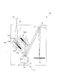
第1の実施形態に係る分光ユニット140は、光ファイバ28を通りファイバカプラ29bから射出される信号光(蛍光)を略平行光束に変換するコリメート光学系41と、この略平行の信号光に含まれる励起光の波長の光を除去する波長選択部148と、回転テーブル42に取り付けられ、それぞれが異なる分光特性を有する3つの分光素子である回折格子431,432,433(回折格子43)と、回折格子431〜433のいずれかで回折された光(分光光)を集光する凹面ミラーからなる集光光学系44と、この集光光学系44で集光された回折光(分光光)を検出する受光器45と、から構成される。
The
この第1の実施形態に係る分光ユニット140において、波長選択部148は、光軸に沿って並んだ、少なくとも2以上のフィルタユニット149を有して構成される。そして、このフィルタユニット149の各々は、互いに異なる波長特性を有する光学素子である平板状のノッチフィルタ149aと、コリメート光学系41と回折格子43との間の光路上にこのノッチフィルタ149aを挿抜するフィルタ挿抜部149bと、ノッチフィルタ149aを回転させることにより、このノッチフィルタ149aに対する信号光(コリメート光学系141で略平行にされた信号光)の入射角度を変化させる回転ステージ149cと、を有して構成されている。
In the
ここで、ノッチフィルタ149aは、予め決められた波長の光を反射し、その他の波長の光を透過するフィルタである。本実施形態においては、例えば、レーザ装置11に用いられる代表的な波長である405nm、488nm、561nm及び640nmに対応した4個のフィルタユニット149が設けられており、それぞれのノッチフィルタ149aがいずれかの波長の光を反射するように構成されている。そのため、図1では図示していないが、情報処理装置50によりレーザ装置11から放射される励起光の波長を制御するとともに、この情報処理装置50を波長選択部148の作動を制御する制御部として用いて、各々のフィルタユニット149のフィルタ挿抜部149bの作動を制御して、レーザ装置11から放射される励起光の波長に対応したノッチフィルタ149aを光路上に挿入し、レーザ装置11から放射されない励起光の波長に対応したノッチフィルタ149aを光路上から抜脱することにより、信号光から不要な励起光を除去するように構成されている。
Here, the
より好ましくは、情報処理装置50によるレーザ装置11から放射される励起光の波長の切り替え制御に同期して、この情報処理装置50により各々のフィルタユニット149のフィルタ挿抜部149bの作動を制御して、レーザ装置11から放射される励起光の波長に対応したノッチフィルタ149aを光路上に挿入し、レーザ装置11から放射されない励起光の波長に対応したノッチフィルタ149aを光路上から抜脱する。
More preferably, the
なお、ノッチフィルタ149aは、複数の波長帯域の光を反射するマルチバンドフィルタを用いることもできる。また、図1においては、4つの波長に対応する4つのフィルタユニット149を設けた構成について説明したが、本発明がこの構成に限定されることはなく、いずれかのノッチフィルタ149aによりレーザ装置11から放射される励起光の波長の光を反射することができれば良い。
Note that the
また、このような第1の実施形態に係る分光ユニット140において、ノッチフィルタ149aのレーザ阻止帯域(反射する光の波長帯域)は狭い方が、観察に用いられる蛍光を除去することがないので好ましいが、このレーザ阻止帯域を狭くしすぎると、レーザ装置11の個体差により、放射される励起光の波長がずれた場合に、励起光が波長選択部148を通過して受光器45に入射してしまう。一般的にノッチフィルタ149aは、このノッチフィルタ149aに光が入射する角度により、レーザ阻止帯域(波長特性)が変化する。具体的には、コリメート光学系41から出射した略平行の信号光がノッチフィルタ149aに垂直に入射する状態(入射角度=0度)からこのノッチフィルタ149aを傾けると、レーザ阻止帯域が短波長側にシフトする。そのため、この分光ユニット140は、レーザ装置11から放射される励起光の波長に合わせて、回転ステージ149cを回転させてノッチフィルタ149aに対する信号光の入射角度を変化させるように構成されている。より好ましくは、情報処理装置50によるレーザ装置11から放射される励起光の波長の切り替え制御に同期して、この情報処理装置50により回転ステージ149cを回転させてノッチフィルタ149aに対する信号光の入射角度を変化させる。この場合、ノッチフィルタ149aに対する信号光の入射角度が0度のときに、励起光のばらつきの長波長側の上限にレーザ阻止帯域が一致するように設計しておくと良い。このように、回転ステージ149cは、ノッチフィルタ149aに入射する光の角度を変化させる角度調整部として機能する。
Further, in the
なお、回転ステージ149cは、ノッチフィルタ149aに対する信号光の入射角度を変化させることが目的であるため、このノッチフィルタ149aを光軸に対して一方向に傾けるように構成されていれば良い。また、ノッチフィルタ149aを15度傾けることができれば、レーザ阻止帯域を3%以上ずらすことが可能であり、十分である。
The
第1の実施形態に係る分光ユニット140を以上のように構成すると、この分光ユニット140に入射する信号光に含まれる励起光の波長の光だけを除去することができ、ノイズの少ない画像を取得することができる。
When the
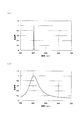
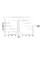
ところで、図3に示すように、上述したノッチフィルタ149aは、透過帯域の分光透過率が一定ではない。全波長帯域に亘って透過率が高いフィルタを設計ししても、図3に示すようにリップル(透過率の細かい凹凸)が存在する。ノッチフィルタ149aのこのような分光透過率特性により、その透過光量が一定でなくなるため、本実施形態に係る分光ユニット40のように、信号光をスペクトル分光する際には、定量的な評価が困難になってしまう。
By the way, as shown in FIG. 3, the above-described
そのため、本実施形態に係る顕微鏡システム1においては、予め、波長選択部148を構成するフィルタユニット149毎に、ノッチフィルタ149aの波長特性(図3に示すようにな、入射光の波長に対する透過率)を測定して情報処理装置50の外部記憶装置(記憶部)54に記憶しておく。なお、ノッチフィルタ149aの波長特性は、実際に測定する代わりに設計値を用いても良い。そして、情報処理装置50は、上述のように光路上に挿入されたノッチフィルタ149aの波長特性(入射角度に応じた波長特性)を外部記憶装置54から読み出し、受光器45で検出された波長対強度の分光信号に対して、上述のノッチフィルタ149aの波長特性で補正をかけることにより精度の高い分光信号を得ることができる。この分光信号に対する補正方法としては、波長毎に補正係数を外部記憶装置54に記憶しておき、この補正係数を受光器45で得られた信号強度に乗算しても良いし、あるいは、受光器45を構成する受光素子45a毎に補正係数に応じてゲインを変えるように構成していも良い。また、複数のノッチフィルタ149aが光路上に配置されている場合には、各々の補正係数を乗算したものを補正係数とすれば良い。
Therefore, in the
また、回転ステージ149cを回転させてノッチフィルタ149aに対する信号光の入射角度を変化させてレーザ阻止帯域を変化させた(シフトさせた)場合は、上述したリップルも波長シフトを起こす。この波長の位相は、後述する式(1)の関係を有しており、波長により異なる。そのため、ノッチフィルタ149aの回転によるリップルのシフト量も波長に依存するため、この変化を考慮して上述の補正を行うことが必要である。
Further, when the
なお、このような、フィルタの波長特性による分光信号の補正は、分光素子としてフィルタを用いた場合も同様に行うことが必要である。 It should be noted that such correction of the spectral signal based on the wavelength characteristics of the filter needs to be performed in the same manner when a filter is used as the spectral element.
[第2の実施形態]
次に、図4〜図8を用いて第2の実施形態に係る分光ユニット240の構成について説明する。なお、この第2の実施形態に係る分光ユニット240も、図1に示す顕微鏡システム1において、分光ユニット40をこの分光ユニット240に置き換えた構成で使用される。そのため、光源系10、共焦点ユニット20及び顕微鏡30を有する共焦点顕微鏡、並びに情報処理装置50の構成は、同一の符号を用いることにより詳細な説明は省略する。また、この第2の実施形態においていも情報処理装置50を波長選択部248の作動を制御する制御部として用いている。
[Second Embodiment]
Next, the configuration of the
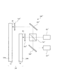
第2の実施形態に係る分光ユニット240は、図4に示すように、光ファイバ28を通りファイバカプラ29bから射出される信号光(蛍光)を略平行光束に変換するコリメート光学系41と、この略平行の信号光に含まれる励起光の波長の光を除去する波長選択部248と、回転テーブル42に取り付けられ、それぞれが異なる分光特性を有する3つの分光素子である回折格子431,432,433(回折格子43)と、回折格子431〜433のいずれかで回折された光を集光する凹面ミラーからなる集光光学系44と、この集光光学系44で集光された回折光を検出する受光器45とから構成される。
As shown in FIG. 4, the
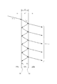
この第2の実施形態に係る分光ユニット240において、波長選択部248は、2つのフィルタユニット249F,249R(これらをまとめて「フィルタユニット249」と呼ぶ)を有して構成される。このフィルタユニット249の各々は、所定の間隔を有して平行に配置された2つの平面S1,S2を有する平板状の光透過部材249a,249bと、平面S1,S2が延びる方向にこれらの光透過部材249a,249bを平行移動させる平行ステージ250aと、この平行ステージ250aを回転させる回転ステージ250bと、から構成される。このフィルタユニット249は、上述の2つの平面S1,S2により、所定の波長の光を透過し、残りの波長の光を反射するように構成されている。なお、光透過部材249a,249bの対向する平面S1,S2には反射膜が形成されており、平行ステージ250aにより移動される方向に沿って、少なくとも2以上の異なる反射率を有する領域を有して構成されている。
In the
ここで、図5に示すように、上述した光透過部材249a,249bの対向する平面S1,S2に挟まれた空間(以下、「干渉空間249c」と呼ぶ)に入射した光束は、2つの平面S1,S2で一部が透過し残りが反射しながら、この干渉空間249c内で反射を繰り返し、これらの平面S1,S2の間で多重干渉を起こす。このとき、図5に示すように、一方の平面(例えば、図5においては平面S1)から入射した光束に関し、この入射光束の干渉空間249cでの入射角度をφ′とし、光束の入射位置での平面S1,S2の間隔(以下、「面間隔」と呼ぶ)をdとし、干渉空間249cの媒質の屈折率をn′として、δを次式(1)のように定義する。なお、図5に示す構成では干渉空間249cには空気が満たされており、屈折率n′はおよそ1である。また、光透過部材249a,249bの媒質の屈折率をnとし、この光透過部材249a,249bにおける上記光束の入射角度をφとすると、スネルの法則により、nsinφ=n′sinφ′が成立する。
Here, as shown in FIG. 5, a light beam incident on a space (hereinafter referred to as “
![]()
![]()
そして、各平面S1,S2のエネルギー反射率をR0とすると、上述のように近接して配置された2つの平面S1,S2の多重干渉によるエネルギー透過率Tfpは、式(1)に示すδを用いて次式(2)のように表される。 Then, assuming that the energy reflectance of each of the planes S1 and S2 is R 0 , the energy transmittance Tfp due to the multiple interference between the two planes S1 and S2 arranged close to each other as described above is expressed by the equation (1) δ. Is expressed as in the following equation (2).
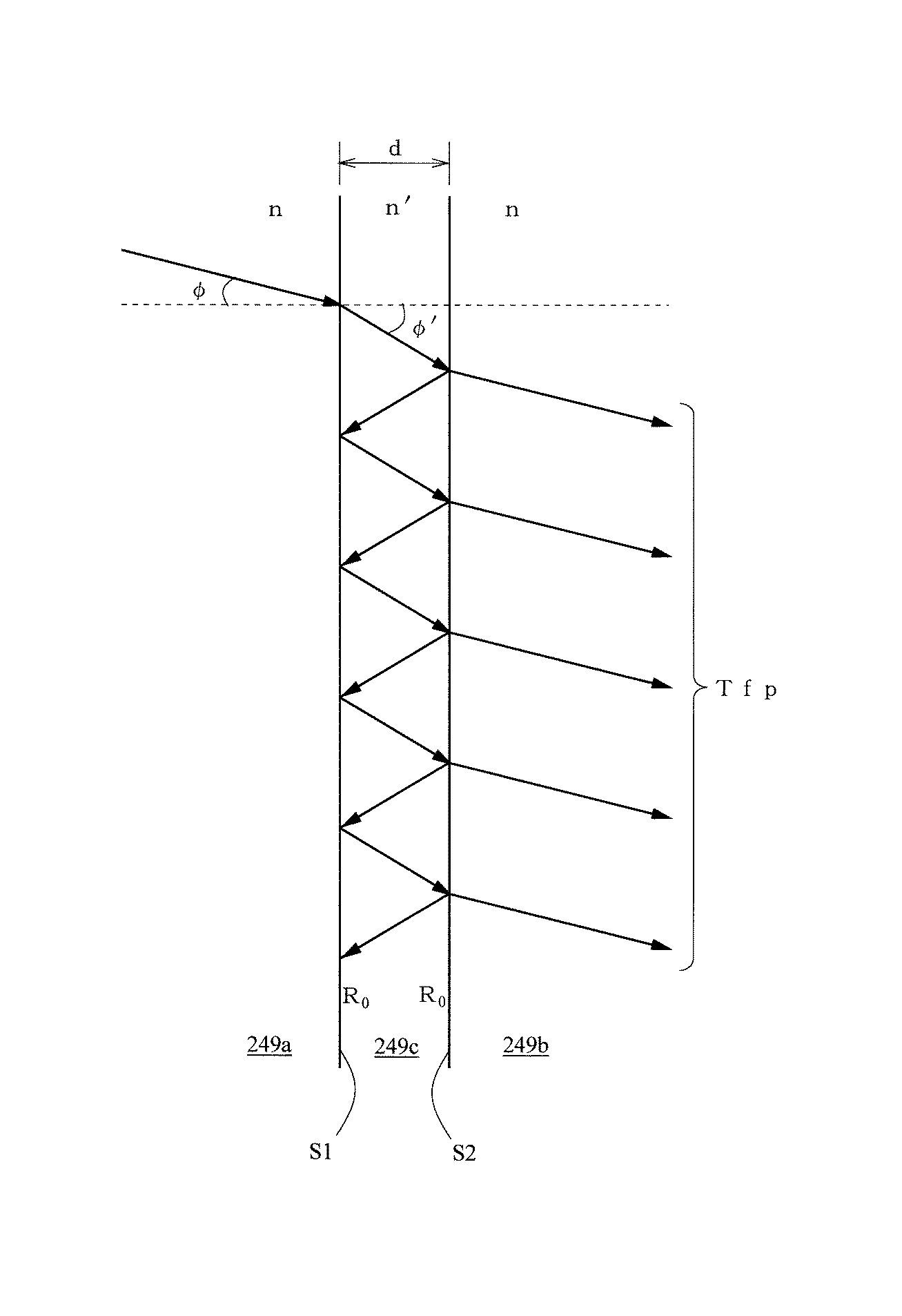
これらの式(1)及び式(2)から明らかなように、上述した構成のフィルタユニット249を透過する光の波長及びこのフィルタユニット249で反射する光の波長の波長特性は、平面S1及び平面S2の反射率R0、これらの平面S1,S2に挟まれた干渉空間32cにおける光束の入射角度φ′及び平面S1及び平面S2の面間隔dにより決定される。
As is clear from these equations (1) and (2), the wavelength characteristics of the wavelength of the light transmitted through the
まず、平面S1,S2の反射率R0について説明する。例えば、干渉空間249cが空気で満たされており(n′=1)、面間隔dが286.4nm、平面S1,S2のエネルギー反射率R0が99%、干渉空間249cにおける光束の入射角度φ′が45°のときのフィルタユニット249の波長特性を図6(a)に示す。なお、この図6は、透過する光の波長特性を示している。このような構成のフィルタユニット249では、405nm付近の波長の光が透過し、それ以外の波長の光が反射する。このとき、透過する光の波長帯域は非常に狭いため、例えば、405nmの光を励起光にし、その他の波長の光を信号光とすることで、信号光から励起光の波長の光だけを確実に除去することができる。
First, the reflectance R 0 of the planes S1 and S2 will be described. For example, the
一方、平面S1,S2の反射率R0を50%とし、その他の条件を上述の構成と同一にしたときのフィルタユニット249の波長特性を図6(b)に示す。このような構成のフィルタユニット249は、上述の図6(a)の場合と透過する光のピーク波長は変わらないが、帯域が広くなるため、このピーク波長の近傍の波長の光も透過してしまい、励起光の波長と信号光の波長とが近接している場合には、信号光までカットされてしまう。そのため、平面S1,S2の反射率R0は90%以上であることが望ましい。
On the other hand, FIG. 6B shows the wavelength characteristics of the
なお、上述したように、この第2の実施形態に係る分光ユニット240において、波長選択部248は、フィルタユニット249の光透過部材249a,249bを、平行ステージ250aにより平面S1,S2の反射率が変化する方向に移動させることができるようになっている。そのため、この平行ステージ250aにより光透過部材249a,249bを移動させ、信号光が入射する位置の反射率を変化させることにより、所望の波長特性を得ることができる。例えば、励起光と信号光の波長が近い場合には、反射率を高くすることにより透過する光の波長帯域を狭くして信号光の損失を防ぎ、励起光と信号光の波長が離れている場合には、反射率を低くして透過する光の波長帯域を広くすることにより励起光を確実にカットすることができる。ここで、平面S1,S2の反射率は平行ステージ250aによる移動方向に連続して変化するようにしても良いし、段階的に変化するようにしても良い。さらに、円状に反射率の異なる膜を成膜しておけば、この光透過部材249a,249bを回転させることにより、信号光が入射する位置の反射率を変化させることができる。このように、平行ステージ250aは、光透過部材249a,249bにおける信号光が入射する位置(反射率の異なる領域)を変化させる位置調整部の機能を有する。
As described above, in the
また、上述の式(1)及び式(2)から明らかなように、平面S1,S2の干渉空間249cにおける光束の入射角度φ′を変化させてもこのフィルタユニット249の波長特性を変化させることができる。光束の入射角度φ′を変化させる場合は、フィルタユニット249の回転ステージ250bにより光透過部材249a,249bを回転させる。すなわち、この回転ステージ250bは、光透過部材249a,249bの平面S1,S2に対する信号光の入射角度を変化させる角度調整部としての機能を有する。なお、これらの平行ステージ250a及び回転ステージ250bの作動は、情報処理装置50によりレーザ装置11から放射される励起光の波長の制御と同期して制御をすることにより、平面S1,S2の反射率や入射角度を変化させて、波長特性を調整することにより、レーザ装置11から放射された励起光の波長の光を信号光から分離することができる。
Further, as apparent from the above formulas (1) and (2), the wavelength characteristic of the
さらに、上述の式(1)及び式(2)から明らかなように、平面S1,S2の面間隔dを変化させてもこのフィルタユニット249の波長特性を変化させることができ、以下に面間隔dを変化させる方法について説明する。図7及び図8に示すように、この第2の実施形態に係る分光ユニット240の波長選択部248を構成するフィルタユニット249は、上述の平面S1,S2が形成された平板状の光透過部材249a,249bを有し、これらの光透過部材249a,249bは、平面S1,S2が対向するように配置されている。この光透過部材249a,249bは、周縁部の3カ所においてスペーサ249dを挟むことにより干渉空間249cを形成するように構成されている。また、このフィルタユニット249は、光透過部材249a,249b及びスペーサ249dを囲むように保持部材249eが設けられている。この保持部材249eは、上述の平面S1,S2を光が透過及び反射可能なように、この平面S1,S2に対して直交する方向から見たときに開口部249jが形成された円環形状を有している。また、図8に示すようにその断面はコの字形状を有しており、この保持部材249eにより囲まれた空間に光透過部材249a,249bの周縁部及びスペーサ249dが配置されている。そして、3つのスペーサ249dの各々の対して位置整合するように保持部材249eの一方の面側に取り付けられた3つの固定部材249fを用いて、光透過部材249a,249b及びスペーサ249dを保持部材249eの他方の面に押しつけてこれらを挟持することにより固定するように構成されている。よって、このフィルタユニット249は、固定部材249fによる押さえつける力を調整することにより、スペーサ249dを押し縮める量を調整し、2つの光透過部材249a,249bの面間隔dを精度良く調整することが可能となる。このように、スペーサ249d、保持部材249e及び固定部材249fは、フィルタユニット249の面間隔dを調整する間隔調整部249gを構成している。
Further, as apparent from the above formulas (1) and (2), the wavelength characteristics of the
なお、上述の説明の間隔調整部249gでは、固定部材249fによるスペーサ249dの押し縮め量で間隔dを調整する場合について説明したが、これらの代わりにピアゾ素子のような圧電効果を利用した素子により面間隔dを調整するように構成しても良いし、ヒーターやペリチェ素子によりスペーサ249dの温度を変化させることによりこのスペーサ249dを膨張・収縮させて面間隔dを調整するように構成しても良い。
In the above-described
また、波長選択部248を構成するフィルタユニット249の平面S1,S2の面間隔dをピアゾ素子のように電気信号により制御する構成の場合、情報処理装置50によりこの面間隔を制御することができる。例えば、情報処理装置50は、標本の性質やレーザ装置11から放射される励起光(照明光)の波長から、標本で発生する蛍光(信号光)の波長を決定し、上述の式(1)及び式(2)を用いて、フィルタユニット249が所望の波長特性となる(励起光を透過し、信号光を反射する)面間隔dを演算により求め、この面間隔dとなるようにフィルタユニット249の間隔調整部249gを制御するように構成することができる。
Further, in the case of a configuration in which the surface interval d between the planes S1 and S2 of the
また、光源系10のレーザ装置11から放射する励起光及びこの励起光により発生する蛍光の波長を入力装置55により入力して情報処理装置50に対して設定し、情報処理装置50で上述の式(1)及び式(2)に基づいて、面間隔d、入射角度φ′及びエネルギー反射率R0の中の少なくとも一つを制御してこのレーザ装置11の波長に連動して波長選択部248(フィルタユニット249(249F,249R))の波長特性を制御するように構成することも可能である。あるいは、外部記憶装置54に、標本33の蛍光色素の種類や、この種類に対応する励起光及び蛍光の波長の少なくとも一つを記憶しておき、入力装置55から入力された蛍光色素の種類や励起光及び蛍光の波長に基づいて、式(1)及び式(2)により面間隔d、入射角度φ′及びエネルギー反射率R0の少なくとも一つを算出して波長選択部248(フィルタユニット249(249F,249R))を調整するように構成しても良い(すなわち、入力装置55から入力された蛍光色素に応じて外部記憶装置54に設定された情報から励起光及び蛍光の波長を決定しても良いし、観察に使用する励起光及び蛍光の波長を直接入力しても良いし、励起光又は蛍光のうちのいずれか一方の波長を入力してそこから他方の波長を決定しても良い)。
Further, the excitation light radiated from the laser device 11 of the
なお、上述の面間隔d及び入射角度φ′は、上記式(1)及び式(2)から算出される値により波長選択部248のフィルタユニット249(249F,249R)を制御しても良いし(例えば、所望の面間隔dになるように光透過部材249a,249bの面間隔を制御する)、予め決められた基準となる位置や、現在の状態における位置に対する補正値(基準となる位置や現在の位置からの差分)として求めて波長選択部248のフィルタユニット249(249F,249R)を制御しても良い。
Note that the above-described surface distance d and incident angle φ ′ may control the filter unit 249 (249F, 249R) of the
また、上述の式(1)及び式(2)より、面間隔dを大きくすることにより、このフィルタユニット249は、2以上の波長を透過するマルチピークとすることもできる。
Further, from the above formulas (1) and (2), the
以上のような構成の分光ユニット240によると、コリメート光学系41で略平行光束となった信号光が第1のフィルタユニット249Fに入射し、この第1のフィルタユニット249Fで、信号光に含まれる所定の波長の光が透過し、その他の波長の光が反射して第2のフィルタユニット249Rに入射する。そして、この第2のフィルタユニット249Rで、信号光に含まれる所定の波長の光が透過し、その他の波長の光が反射して回折格子431〜433のいずれかで回折されて集光光学系44で集光され、受光器45で検出される。そのため、波長選択部238の第1及び第2のフィルタユニット249F,249Rの波長特性を上述した方法により調整することにより、この波長選択部238により、信号光に含まれる励起光の波長の光を透過させることで除去することができるので、ノイズの少ない画像を取得することができる。
According to the
このとき、上述のように2つのフィルタユニット249F,249Rを組み合わせることにより、それぞれのフィルタユニットに対する信号光の入射角度が同じになるようにすると、すなわち、第1及び第2のフィルタユニット249F,249Rの平面S1,S2が略平行になるようにすると、信号光の入射角度に拘わらず波長選択部238の同じ位置から同じ方向に信号光が射出される。そのため、回折格子43以降の光学系の位置は固定することができる。なお、2つのフィルタユニット249F,249Rの一方をミラーで構成することも可能である。その場合、ミラーに対しては、回転ステージは必要であるが、平行ステージを設ける必要は無い。
At this time, by combining the two
また、以上の説明では、フィルタユニット249(249F,249R)の面間隔d、入射角度φ′及びエネルギー反射率R0の少なくとも一つを制御して波長選択部248を所望の波長特性となるように構成しているが、第1及び第2のフィルタユニット249F,249Rの各々に、波長特性を検出する検出部260を設けても良い。この場合、波長選択部248のフィルタユニット249(249R,249F)の波長特性を確認するだけでなく、検出部260で検出される波長特性をフィードバックして面間隔d、入射角度φ′又はエネルギー反射率R0の値を調整することにより、この波長選択部248全体の波長特性が所望の値になるように制御することも可能である。この検出部260によるフィルタユニット249(249F,249R)の波長特性の検出方法としては、光透過部材249a,249bの平面S1,S2の間隔を検知することにより検出する方法があり、以下にその構成を説明する。
In the above description, at least one of the surface distance d, the incident angle φ ′, and the energy reflectance R 0 of the filter unit 249 (249F, 249R) is controlled so that the
まず、図9(a)を用いて透過光及び反射光の強度比率からフィルタユニット249の波長特性を検出する検出部260の構成について説明する。この検出部260は、異なる波長の光であって、これらの光が略平行に進んで光透過部材249aに所定の入射角度で入射する光を放射する第1の光源261及び第2の光源262と、第1の光源261から放射され光透過部材249a,249bを透過した光を検出する第1の透過センサ263、及び、第1の光源261から放射され光透過部材249bの平面S1,S2の多重干渉で反射して光透過部材249aを透過した光を検出する第1の反射センサ264と、第2の光源262から放射され光透過部材249a,249bを透過した光を検出する第2の透過センサ265、及び、第2の光源262から放射され光透過部材249bの平面S1,S2の多重干渉で反射して光透過部材249aを透過した光を検出する第2の反射センサ266と、から構成されている。なお、ここでは、第1の光源261から放射される光の波長を400nmとし、第2の光源262から放射される光の波長を550nmとし、第1及び第2の光源261,262から放射された光の光透過部材249aへの入射角度を15°とし、また、フィルタユニット249の平面S1,S2のエネルギー反射率を80%、間隔dを300nmとして、図10に示す波長特性を有しているものとして説明する。
First, the configuration of the
フィルタユニット249の波長特性は、上述したように、平面S1及び平面S2に挟まれた干渉空間における光束の入射角度、平面S1及び平面S2の間隔並びにエネルギー反射率により決定される。すなわち、これらの値が適切な値であれば、この検出部260において、第1の光源261に対応した第1の透過センサ263及び第1の反射センサ264で検出される光の強度は、第1の光源261から放射される光の波長が400nmであることから、図10に示すようにフィルタユニット249の透過率が95%、反射率が5%となるため、この比率に応じた値となる。同様に、第2の光源262に対応した第2の透過センサ265及び第2の反射センサ266で検出される光の強度は、第2の光源262から放射される光の波長が550nmであることから、図10に示すようにフィルタユニット249の透過率が50%、反射率が50%となるため、この比率に応じた値となる。図9(a)に示すように、第1及び第2の光源261,262から放射された光の入射角度を、分光ユニット240における信号光の入射角度に設定し、上記センサ263,264,265,266で検出される光の強度が上述した割合になるように光透過部材249a,249bの間隔を調整することにより、フィルタユニット249の波長特性を所望の値に設定することができる。
As described above, the wavelength characteristic of the
次に、図9(b)を用いてアライメント顕微鏡によりフィルタユニット249の波長特性を検出する検出部260′の構成について説明する。この検出部260′は、フィルタユニット249を構成する2つの光透過部材249a,249bのそれぞれの位置を正確に計測するため、光透過部材249aには第1のアライメント顕微鏡261′及び第3のアライメント顕微鏡263′を配置し、光透過部材249bに対しては第2のアライメント顕微鏡262′及び第4のアライメント顕微鏡264′をそれぞれ配置して構成している。これにより、それぞれの光透過部材249a,249bを形成する各平面S1,S2の位置、あるいは光透過部材249a,249bの側面部に形成されたアライメントマーク(不図示)の位置を精密に計測することで、フィルタユニット249の波長特性を検出する、すなわち、これにより光透過部材249aと光透過部材249bとの間隔を所望の値に設定している。なお、2つの光透過部材249a,249b(平面S1,S2)の間隔を、より平行に設定するためにはそれぞれの光透過部材249a,249bに対して概ね120度の間隔を空けて3組のアライメント顕微鏡を配置するのが良い。またシステムを簡略化するためには光透過部材249aと光透過部材249bのうちのどちらか片方の最低一箇所にアライメント顕微鏡を配置すればよい。
Next, the configuration of the
最後に、図11を用いて測長干渉計によりフィルタユニット249の波長特性を検出する検出部260″の構成について説明する。この検出部260″は、フィルタユニット249を構成する2つの光透過部材249a,249bのそれぞれの位置を正確に計測するため、それぞれの同一方向の側面に反射面R1,R2を設けて測長干渉計を構成する。具体的には、干渉計ヘッド261″から出射した光束を偏光ビームスプリッタ262″にてP波及びS波に分離し、この偏光ビームスプリッタ262″を透過したP波は光透過部材249bの反射面R2に、偏光ビームスプリッタ262″で反射したS波は第1のミラー263″にて光透過部材249aの反射面R1に入射させる。ここで、この偏光ビームスプリッタ262″で分離された2つの光路のいずれにも第1のλ/4板264″及び第2のλ/4板265″が配置されている。そのため、光透過部材249a,249bのそれぞれの反射面R1,R2にて反射して再び偏光ビームスプリッタ262″に入射する際に偏光方向が90度変換されることになる。すなわち、光透過部材249aの反射面R1で反射した光はP波になって第1のミラー263″で反射され、偏光ビームスプリッタ262″を透過し、光透過部材249bの反射面R2で反射した光はS波になって偏光ビームスプリッタ262″で反射されることにより、これらの光が合成されて第2のミラー266″に入射し、この第2のミラー266″で反射されてレシーバー267″に入射する。このレシーバー267″より出力される出力信号、すなわちフィルタユニット249の波長特性に基づいて光透過部材249a,249bの間隔を正確に制御することができる。
Finally, the configuration of a
なお、図10に示す検出部260″においては、干渉計を一つだけ配置しているが、より理想的には複数の干渉計を配置して制御することで光透過部材249a,249bの平行度を良好に保つことが可能となり好ましい。
In the
なお、以上の第1及び第2の実施形態に係る分光ユニット140,240においては、波長選択部148,248を回折格子43に入射する手前に配置したが、本発明がこの構成に限定されることはなく、光ファイバ28の射出端(ファイバカプラ29b)から受光器45までの間の光路上であればどこに配置しても良い。
In the
1 顕微鏡システム 29b ファイバカプラ(射出端)
10 光源系(光源) 30 顕微鏡 32 対物レンズ 33 標本
40 分光ユニット(分光部) 41 コリメート光学系
43(431〜433) 回折格子(分光素子) 44 集光光学系
45 受光器 50 情報処理装置(制御部) 54 外部記憶装置(記憶部)
140 分光ユニット 148 波長選択部 149 フィルタユニット
149a ノッチフィルタ(光学素子) 149b フィルタ挿抜部
149c 回転ステージ(角度調整部) 240 分光ユニット
248 波長選択部 249(249F,249R) フィルタユニット
249a,249b 光透過部材(光学素子) 249g 間隔調整部
250a 平行ステージ(位置調整部) 250b 回転ステージ(角度調整部)
1
DESCRIPTION OF
140
Claims (12)
前記顕微鏡からの前記蛍光を分光する分光素子、及び該分光素子により分光された分光光を受光する受光器を含む分光部と、
を有する顕微鏡システムであって、
前記分光部は、前記励起光が前記受光器に向かうことを抑制し、前記蛍光を前記受光器に導く波長選択部を有し、
前記波長選択部を制御して前記励起光の波長に対応させて前記波長選択部の波長特性を変化させる制御部を備えることを特徴とする顕微鏡システム。 A microscope that scans the excitation light emitted from the light source and collects it on the sample by the objective lens, and collects the fluorescence from the sample on the objective lens,
A spectroscopic element that splits the fluorescence from the microscope, and a spectroscopic unit that receives the spectroscopic light split by the spectroscopic element;
A microscope system comprising:
The spectroscopic unit includes a wavelength selection unit that suppresses the excitation light from being directed to the light receiver and guides the fluorescence to the light receiver.
A microscope system comprising: a control unit that controls the wavelength selection unit to change a wavelength characteristic of the wavelength selection unit according to the wavelength of the excitation light.
波長特性が異なる2以上の光学素子と、
前記光学素子の各々を前記分光部の光路に挿抜するフィルタ挿抜部と、を有し、
前記制御部は、前記フィルタ挿抜部を制御することにより、前記光学素子の少なくとも一つを前記光路上に挿入し、その他の前記光学素子を前記光路上から抜脱することを特徴とする請求項1に記載の顕微鏡システム。 The wavelength selector is
Two or more optical elements having different wavelength characteristics;
A filter insertion / extraction section for inserting / extracting each of the optical elements into / from the optical path of the spectroscopic section,
The control unit controls the filter insertion / extraction unit to insert at least one of the optical elements on the optical path and to remove the other optical elements from the optical path. The microscope system according to 1.
前記制御部は、前記角度調整部を制御することを特徴とする請求項1に記載の顕微鏡システム。 The wavelength selection unit includes an optical element having a predetermined wavelength characteristic, and includes an angle adjustment unit that changes an incident angle of the excitation light with respect to the optical element,
The microscope system according to claim 1, wherein the control unit controls the angle adjustment unit.
前記記憶部から読み出された前記入射角度になるように、前記制御部により前記角度調整部を制御することを特徴とする請求項3に記載の顕微鏡システム。 A storage unit that stores the incident angle of the angle adjustment unit controlled by the control unit in association with the wavelength of the excitation light;
The microscope system according to claim 3, wherein the angle adjustment unit is controlled by the control unit so that the incident angle is read from the storage unit.
前記制御部により前記間隔調整部及び前記角度調整部の少なくとも一方を制御することを特徴とする請求項1に記載の顕微鏡システム。 The wavelength selection unit includes two light transmission members arranged so that planes having a predetermined reflectance face each other at a predetermined interval, an interval adjustment unit that changes the interval, and the excitation light for the light transmission member, A filter unit including at least one of angle adjustment units that change the incident angle of the fluorescence;
The microscope system according to claim 1, wherein at least one of the interval adjustment unit and the angle adjustment unit is controlled by the control unit.
前記記憶部から読み出された前記間隔になるように、前記制御部により前記間隔調整部を制御する請求項6に記載の顕微鏡システム。 A storage unit that stores the interval of the interval adjustment unit controlled by the control unit in association with the wavelength of the excitation light;
The microscope system according to claim 6, wherein the interval adjustment unit is controlled by the control unit so as to be the interval read from the storage unit.
前記記憶部から読み出された前記入射角度になるように、前記制御部により前記角度調整部を制御する請求項6に記載の顕微鏡システム。 A storage unit that stores the incident angle of the angle adjustment unit controlled by the control unit in association with the wavelength of the excitation light;
The microscope system according to claim 6, wherein the angle adjustment unit is controlled by the control unit so that the incident angle is read from the storage unit.
2つの前記光透過部材は、光軸に直交する面内を移動させて前記励起光が入射する前記領域を変化させる位置調整部を有することを特徴とする請求項6〜9のいずれか一項に記載の顕微鏡システム。 Each of the planes of the light transmission member is formed with at least two or more regions having different reflectivities,
The two light transmissive members include a position adjusting unit that moves in a plane orthogonal to the optical axis to change the region where the excitation light is incident. 10. The microscope system described in 1.
前記第1の光学素子で反射された前記光のうち、少なくとも前記蛍光を含む光を反射する第2の光学素子と、を有し、
前記第1の光学素子及び前記第2の光学素子のうちの少なくとも一方は、前記フィルタユニットであることを特徴とする請求項6〜10のいずれか一項に記載の顕微鏡システム。 The wavelength selection unit includes a first optical element that reflects at least the fluorescence-containing light among incident light; and
A second optical element that reflects at least the light containing the fluorescent light among the light reflected by the first optical element;
The microscope system according to claim 6, wherein at least one of the first optical element and the second optical element is the filter unit.
Priority Applications (1)
| Application Number | Priority Date | Filing Date | Title |
|---|---|---|---|
| JP2012066820A JP2013200329A (en) | 2012-03-23 | 2012-03-23 | Microscope system |
Applications Claiming Priority (1)
| Application Number | Priority Date | Filing Date | Title |
|---|---|---|---|
| JP2012066820A JP2013200329A (en) | 2012-03-23 | 2012-03-23 | Microscope system |
Publications (1)
| Publication Number | Publication Date |
|---|---|
| JP2013200329A true JP2013200329A (en) | 2013-10-03 |
Family
ID=49520651
Family Applications (1)
| Application Number | Title | Priority Date | Filing Date |
|---|---|---|---|
| JP2012066820A Pending JP2013200329A (en) | 2012-03-23 | 2012-03-23 | Microscope system |
Country Status (1)
| Country | Link |
|---|---|
| JP (1) | JP2013200329A (en) |
Cited By (1)
| Publication number | Priority date | Publication date | Assignee | Title |
|---|---|---|---|---|
| US20220170857A1 (en) * | 2020-11-27 | 2022-06-02 | Wistron Corporation | Detection device and method therefor |
Citations (8)
| Publication number | Priority date | Publication date | Assignee | Title |
|---|---|---|---|---|
| JP2002228663A (en) * | 2001-02-05 | 2002-08-14 | I Bio:Kk | Fluorescent immunity-measuring instrument |
| JP2006276840A (en) * | 2005-03-03 | 2006-10-12 | Olympus Corp | Microscope apparatus, control unit thereof, and program |
| JP2008299207A (en) * | 2007-06-01 | 2008-12-11 | Nikon Corp | Variable filter device and confocal microscope |
| JP2009115546A (en) * | 2007-11-05 | 2009-05-28 | Fujifilm Corp | Analyzer |
| JP2009244156A (en) * | 2008-03-31 | 2009-10-22 | Nikon Corp | Spectroscopic device and spectral confocal microscope |
| JP2010096913A (en) * | 2008-10-15 | 2010-04-30 | Olympus Corp | Laser microscope device |
| JP2010160043A (en) * | 2009-01-08 | 2010-07-22 | Panasonic Corp | Surface intensifying raman spectrophotometric method, and surface intensifying raman spectrophotometric apparatus using the same |
| JP2012003196A (en) * | 2010-06-21 | 2012-01-05 | Olympus Corp | Laser scanning microscope |
-
2012
- 2012-03-23 JP JP2012066820A patent/JP2013200329A/en active Pending
Patent Citations (8)
| Publication number | Priority date | Publication date | Assignee | Title |
|---|---|---|---|---|
| JP2002228663A (en) * | 2001-02-05 | 2002-08-14 | I Bio:Kk | Fluorescent immunity-measuring instrument |
| JP2006276840A (en) * | 2005-03-03 | 2006-10-12 | Olympus Corp | Microscope apparatus, control unit thereof, and program |
| JP2008299207A (en) * | 2007-06-01 | 2008-12-11 | Nikon Corp | Variable filter device and confocal microscope |
| JP2009115546A (en) * | 2007-11-05 | 2009-05-28 | Fujifilm Corp | Analyzer |
| JP2009244156A (en) * | 2008-03-31 | 2009-10-22 | Nikon Corp | Spectroscopic device and spectral confocal microscope |
| JP2010096913A (en) * | 2008-10-15 | 2010-04-30 | Olympus Corp | Laser microscope device |
| JP2010160043A (en) * | 2009-01-08 | 2010-07-22 | Panasonic Corp | Surface intensifying raman spectrophotometric method, and surface intensifying raman spectrophotometric apparatus using the same |
| JP2012003196A (en) * | 2010-06-21 | 2012-01-05 | Olympus Corp | Laser scanning microscope |
Cited By (1)
| Publication number | Priority date | Publication date | Assignee | Title |
|---|---|---|---|---|
| US20220170857A1 (en) * | 2020-11-27 | 2022-06-02 | Wistron Corporation | Detection device and method therefor |
Similar Documents
| Publication | Publication Date | Title |
|---|---|---|
| NL1034256C2 (en) | Spectroscopy system. | |
| NL1032793C2 (en) | Spectroscopy system. | |
| JP5092104B2 (en) | Spectrometer and spectroscopic method | |
| US7365842B2 (en) | Light scanning type confocal microscope | |
| JP5945400B2 (en) | Detection optical system and scanning microscope | |
| US20130258332A1 (en) | Microscope spectrometer, optical axis shift correction device, spectroscope and microscope using same | |
| KR101078135B1 (en) | Full range calibration apparatus for light spectrum analysis and method for acquisition information in calibration apparatus | |
| JP5517621B2 (en) | High sensitivity spectrum analysis unit | |
| KR20130123190A (en) | Spectral fluorescence lifetime imaging microscope with the use of tunable bandpass filters | |
| CN102246015A (en) | Monochromator comprising variable wavelength selector in combination with tunable interference filter | |
| KR20190038994A (en) | Confocal measurement device | |
| JP4434882B2 (en) | Laser scanning fluorescence observation system | |
| JP4645176B2 (en) | Spectroscopic microscope | |
| JP2012526972A (en) | Compact confocal spectrometer | |
| JP4311936B2 (en) | Laser scanning microscope | |
| JP2013200329A (en) | Microscope system | |
| JP7486178B2 (en) | Spectroscopic equipment | |
| JP5576649B2 (en) | Spectroscope and optical apparatus provided with the same | |
| JP2009244156A (en) | Spectroscopic device and spectral confocal microscope | |
| JP5787151B2 (en) | Spectroscopic unit and scanning microscope | |
| CN210571973U (en) | micro-Raman system with optical tweezers | |
| JP4336847B2 (en) | Microspectrophotometer | |
| JP2006300808A (en) | Raman spectrometry system | |
| CN111272732A (en) | Raman spectrometer and Raman spectrum splicing method | |
| JP2006276840A (en) | Microscope apparatus, control unit thereof, and program |
Legal Events
| Date | Code | Title | Description |
|---|---|---|---|
| A621 | Written request for application examination |
Free format text: JAPANESE INTERMEDIATE CODE: A621 Effective date: 20141208 |
|
| A977 | Report on retrieval |
Free format text: JAPANESE INTERMEDIATE CODE: A971007 Effective date: 20151111 |
|
| A131 | Notification of reasons for refusal |
Free format text: JAPANESE INTERMEDIATE CODE: A131 Effective date: 20151210 |
|
| A521 | Request for written amendment filed |
Free format text: JAPANESE INTERMEDIATE CODE: A523 Effective date: 20160208 |
|
| A131 | Notification of reasons for refusal |
Free format text: JAPANESE INTERMEDIATE CODE: A131 Effective date: 20160728 |
|
| A601 | Written request for extension of time |
Free format text: JAPANESE INTERMEDIATE CODE: A601 Effective date: 20160923 |
|
| A02 | Decision of refusal |
Free format text: JAPANESE INTERMEDIATE CODE: A02 Effective date: 20170201 |