JP2013165149A - Multilayer ceramic substrate and manufacturing method of the same - Google Patents
Multilayer ceramic substrate and manufacturing method of the same Download PDFInfo
- Publication number
- JP2013165149A JP2013165149A JP2012027045A JP2012027045A JP2013165149A JP 2013165149 A JP2013165149 A JP 2013165149A JP 2012027045 A JP2012027045 A JP 2012027045A JP 2012027045 A JP2012027045 A JP 2012027045A JP 2013165149 A JP2013165149 A JP 2013165149A
- Authority
- JP
- Japan
- Prior art keywords
- conductor
- extension
- ceramic substrate
- multilayer ceramic
- paste
- Prior art date
- Legal status (The legal status is an assumption and is not a legal conclusion. Google has not performed a legal analysis and makes no representation as to the accuracy of the status listed.)
- Pending
Links
Images


Abstract
Description
本発明は、多層セラミック基板、およびその製造方法に関する。 The present invention relates to a multilayer ceramic substrate and a manufacturing method thereof.
今日、多層セラミック基板は、高周波回路のパッケージ基板として広く用いられている。近年、機器の小型化と低コスト化のため基板サイズは小さくなってきており、搭載部品や外部機器との信号接続を行うための接続用導体パットはより小さく、高密度化している。 Today, multilayer ceramic substrates are widely used as package substrates for high-frequency circuits. In recent years, the substrate size has been reduced due to the downsizing and cost reduction of devices, and the connecting conductor pads for signal connection with mounted components and external devices are smaller and higher in density.
多層セラミック基板と外部機器の配線は、はんだ付け、ワイヤボンド、リボンボンド等により接合されることが多い。この接合は熱圧着、超音波接合等により施され、基板に形成される接続用導体パットは、接合に必要な最小限のサイズとなっている。そのため、基板端面に近い部分に接続用導体パットが形成され、接続用導体パットの面積は上記接合の所要面積にほぼ等しくなっている。特にリボンボンド接合においては、接続相手との距離を短くする必要上から、接続用導体パットの端部近傍まで接合部分が及ぶことが多い。このため外部機器とセラミック基板との接合部において、線膨張率差に起因する応力が発生し、特に接続用導体パットの端部に応力が集中する。その結果、接続用導体パットが端部から剥離しやすいという問題がある。 The wiring between the multilayer ceramic substrate and the external device is often joined by soldering, wire bonding, ribbon bonding or the like. This joining is performed by thermocompression bonding, ultrasonic joining, or the like, and the connecting conductor pad formed on the substrate has a minimum size necessary for joining. For this reason, a connecting conductor pad is formed in a portion close to the end face of the substrate, and the area of the connecting conductor pad is substantially equal to the required area for joining. In particular, in the ribbon bond joining, the joining portion often extends to the vicinity of the end of the connecting conductor pad from the necessity of shortening the distance to the connection partner. For this reason, stress due to the difference in linear expansion coefficient is generated at the joint between the external device and the ceramic substrate, and the stress is concentrated particularly on the end portion of the connecting conductor pad. As a result, there is a problem that the connecting conductor pad is easily peeled off from the end.
また、接続用導体パットは、その導体の酸化を防ぐためにニッケルを下地とした金めっきが施されることが多い。金めっきによるニッケルの腐食作用により、パット端部にダメージを負い密着強度は更に弱くなることが確認されている。 Further, the connection conductor pad is often subjected to gold plating with nickel as a base in order to prevent oxidation of the conductor. It has been confirmed that due to the corrosive action of nickel caused by gold plating, the pad end is damaged and the adhesion strength is further reduced.
特許文献1には、以上の課題を解決する方法として、誘電体ペーストを用いてスクリーン印刷法により電極パットの一部を誘電体層で覆い、密着力を上げる方法が記載されている。また、特許文献2によれば、接続用導体パットのメタライズ強度を向上させる方法として、導体ペースト中の金属粒子径や、膜厚を厚くする方法が記載されている。
しかしながら、特許文献1に示す従来の製造方法では、接続用導体パットの表面の一部が誘電体で覆われることになり、パットサイズ小さくなって接続が難しくなる。また、補強用の誘電体ペーストが接続用導体パット周辺に盛り上がる形となり、接合に支障を生じる。
However, in the conventional manufacturing method shown in
また、特許文献2に示す従来の製造方法では、導体ペースト中の金属粒子径や、膜厚を厚くすることは、特に接続用導体パット端部の密着を何ら改善するものではなく、逆にセラミック基板全体の反りの原因となる問題があった。
Further, in the conventional manufacturing method shown in
本発明は上記に鑑みてなされたものであって、多層セラミック基板の接続用導体パット端部における密着強度を確保するとともに、剥離を抑制する多層セラミック基板、およびその製造方法を提供することを目的とする。 The present invention has been made in view of the above, and an object of the present invention is to provide a multilayer ceramic substrate that secures adhesion strength at the end of the connecting conductor pad of the multilayer ceramic substrate and suppresses peeling, and a method for manufacturing the same. And
本発明による多層セラミック基板は、多層に積層されたセラミック層と、上記セラミック層の表面に形成された導体部、及び当該導体部の端部から延在した延長部からなる導体パットと、を備え、上記延長部が上記セラミック層の内部に形成されたことを特徴とする。また、上記延長部は、上記セラミック層の内部の斜め下方もしくは真下に向かって延在しても良い。また、上記延長部は、上記セラミック層の内部でU字形状に屈曲しても良い。 A multilayer ceramic substrate according to the present invention includes a multilayered ceramic layer, a conductor part formed on a surface of the ceramic layer, and a conductor pad including an extension extending from an end of the conductor part. The extension is formed in the ceramic layer. The extension may extend obliquely downward or directly below the ceramic layer. The extension may be bent in a U shape inside the ceramic layer.
また、本発明による多層セラミック基板の製造方法は、積層されたグリーンシートに導体ペーストを印刷した後、当該導体ペーストの上表面もしくは周囲端部に面してセラミックペーストを印刷する印刷工程と、上記印刷工程後、上記導体ペーストおよびセラミックペーストを押圧するプレス工程と、上記プレス工程後、上記グリーンシートを焼成する焼成工程と、を備えて、セラミック層表面に形成される導体部の端部から延在する延長部を、当該セラミック層の内部に形成するものであっても良い。 The method for manufacturing a multilayer ceramic substrate according to the present invention includes a printing step of printing a ceramic paste so as to face an upper surface or a peripheral edge of the conductive paste after printing the conductive paste on the laminated green sheets; A pressing step for pressing the conductor paste and the ceramic paste after the printing step, and a firing step for firing the green sheet after the pressing step, and extending from the end of the conductor portion formed on the surface of the ceramic layer. The existing extension may be formed inside the ceramic layer.
本発明によれば、基板端部の接続用導体パットにおいて、十分な接合強度を有する多層セラミック基板が簡易に製造でき、品質向上に寄与する。 According to the present invention, a multi-layer ceramic substrate having sufficient bonding strength can be easily manufactured in the connecting conductor pad at the end of the substrate, contributing to quality improvement.
以下に、本発明に係る多層セラミック基板の製造方法の実施の形態を、図面に基づいて詳細に説明する。なお、この実施の形態により、この発明が限定されるものではなく、当該実施の形態には、当業者が容易に想到できるものや実質的に同一のものが含まれることは言うまでもない。 Hereinafter, embodiments of a method for producing a multilayer ceramic substrate according to the present invention will be described in detail with reference to the drawings. Note that the present invention is not limited to the embodiments, and it goes without saying that the embodiments include those that can be easily conceived by those skilled in the art and those that are substantially the same.
実施の形態1.
図1は、本発明に係る実施の形態1による多層セラミック基板の構成を示す図であり、(a)は断面模式図、(b)は接続用導体パット端部を拡大した断面模式図である。図2は、実施の形態1による多層セラミック基板の接続用導体パットが設けられた図1(a)の部分1を拡大した断面模式図であり、(a)は第1の態様の平面図、(b)は第2の態様の平面図である。図1、2において、実施の形態1による多層セラミック基板10は、多層に積層されてなるセラミック層2と、セラミック層2の上に形成された接続用導体パット20を含む導体パットから構成される。接続用導体パット20は、セラミック層2の上に形成された導体部3と、更に導体部3の上に形成されためっき層4からなる。導体部3は、その端部から延長された導体延長部3aがつながっており、この導体延長部3aはセラミック層2の内部に埋没している。
1A and 1B are diagrams showing a configuration of a multilayer ceramic substrate according to a first embodiment of the present invention. FIG. 1A is a schematic cross-sectional view, and FIG. . 2 is an enlarged schematic cross-sectional view of a
図2は、実施の形態1による多層セラミック基板の接続用導体パットの端部形状を拡大した模式図であり、(a)は第1態様の端部形状の平面図、(b)は第2態様の端部形状の平面図である。図3は、実施の形態1による多層セラミック基板の接続用導体パットの端部形状を拡大した模式図であり、(a)は第3態様の端部形状の平面図、(b)は第4態様の端部形状の平面図、(c)は第5態様の端部形状の平面図、(d)は第6態様の端部形状の平面図である。なお、導体部3の上にはめっき層4が形成されているが、ここではめっき層4の図示を省略して、基板表面に導体部3が露出した状態で図示している。また、基板内部に埋没している導体延長部3aは破線で示す。
FIG. 2 is an enlarged schematic view of the end shape of the connecting conductor pad of the multilayer ceramic substrate according to the first embodiment, where (a) is a plan view of the end shape of the first mode, and (b) is a second view. It is a top view of the edge part shape of an aspect. FIG. 3 is an enlarged schematic view of the end shape of the connecting conductor pad of the multilayer ceramic substrate according to the first embodiment. FIG. 3A is a plan view of the end shape of the third mode, and FIG. The top view of the end shape of an aspect, (c) is a top view of the end shape of a 5th aspect, (d) is a top view of the end shape of a 6th aspect. In addition, although the
図2(a)の第1態様に示す通り、多層セラミック基板10の接続用導体パット20の端部は、基板表面に露出した導体部3および基板内部に埋没している導体延長部3aが、何れも角部が直角であっても良い。また、図2(b)の第2態様に示す通り、基板内部に埋没している導体延長部3bは、基板表面に露出した導体部3の幅より狭くなっており、角部が面取りされている。
As shown in the first embodiment of FIG. 2 (a), the end portion of the connecting
また、図3(a)の第3態様に示す通り、基板内部に埋没している導体延長部3cは、基板表面に露出した導体部3の幅より狭くなっており、端部が三角形状になっている。また、図3(b)の第4態様に示す通り、基板内部に埋没している導体延長部3dは、基板表面に露出した導体部3の幅より狭くなっており、端部が半円形状になっている。
3A, the conductor extension 3c embedded in the substrate is narrower than the width of the
また、図3(c)の第5態様に示す通り、基板内部に埋没している導体延長部3eは、その幅が基板表面に露出した導体部3の幅よりも台形状に僅かに拡がり、角が直角をなす形状になっている。また、図3(d)の第6態様に示す通り、基板内部に埋没している導体延長部3fは、その幅が基板表面に露出した導体部3の幅よりも僅かに大きく、角が直角をなす矩形状になっている。このように、導体延長部3e,3fは、基板表面に露出した導体部3の幅より拡げることで、接続用導体パット20の配線ピッチの小型化にはやや不利であるものの、接続用導体パット20の耐剥離性はより向上することとなる。
Further, as shown in the fifth mode of FIG. 3 (c), the conductor extension 3e buried in the substrate has a width that is slightly wider in a trapezoidal shape than the width of the
更に、図4は、実施の形態1に係る接続用導体パット端部の形状を示す図であり、(a)は第7態様の平面図、(b)は第8態様の平面である。基板内部に埋没している導体延長部3gは、図4(a)、(b)における導体延長部3g、3hのように、接続用導体パットの導体部3の端部より延長された導体の全てまたは一部を、幅の狭い幾つかの導体に分割しても良い。図4(a)の導体延長部3gは3つの導体に分割された例、図4(b)の導体延長部3hは2つの導体に分割された例を示している。
Furthermore, FIG. 4 is a figure which shows the shape of the connection conductor pad edge part which concerns on
なお、これまで述べた図2乃至図4の導体延長部3a乃至3hの各態様は、単独で形成しても良いし、複合した形状としても良い。
Each of the embodiments of the
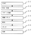
次に、多層セラミック基板10の製造方法について説明する。図5は、実施の形態1に係る多層セラミック基板10の製造方法を示すフローチャートである。
まず、VIA(ビア)導体を形成するためにVIAホールを形成する穴あけ(穴あけ工程)を実行する(ステップS1)。
この穴あけ工程は、複数枚のセラミックグリーンシート(以下「グリーンシート」と表記する)に対して、パンチングなどの方法で穴を形成する工程である。使用するグリーンシートは、例えば厚さ100μm、形成する穴は例えば150μmである。
Next, a method for manufacturing the multilayer
First, in order to form a VIA (via) conductor, a drilling (drilling process) for forming a VIA hole is executed (step S1).
This drilling step is a step of forming holes in a plurality of ceramic green sheets (hereinafter referred to as “green sheets”) by a method such as punching. The green sheet to be used has a thickness of, for example, 100 μm, and the hole to be formed has, for example, 150 μm.
穴あけ工程が完了した後、穴あけ工程で形成したVIAホールに導体ペーストを充填する工程(VIA充填工程)を行う(ステップS2)。
このVIA充填工程では、例えばスクリーン印刷法を用いて導体ペーストが充填される。
After the drilling process is completed, a process of filling the VIA hole formed in the drilling process with the conductive paste (VIA filling process) is performed (step S2).
In this VIA filling step, the conductor paste is filled using, for example, a screen printing method.
VIA充填工程が完了した後、配線などの導体パターンをグリーンシートに印刷する工程(パターン印刷工程)を行う(ステップS3)。
導体パターンを印刷するに当たっては、例えばスクリーン印刷法を用いる。このようにして、必要な種類、枚数を同様に用意する。
After the VIA filling process is completed, a process (pattern printing process) of printing a conductor pattern such as wiring on a green sheet is performed (step S3).
For printing the conductor pattern, for example, a screen printing method is used. In this manner, necessary types and numbers are prepared in the same manner.
パターン印刷工程が完了した後、積層・プレス工程を行う(ステップS4)。
この積層・プレス工程は、VIA導体および導体パターンが形成されたグリーンシートを積層させてプレスする工程である。グリーンシートを積層する際は、例えば、平面上の同一箇所に加工された穴を合わせることによって、グリーンシート同士の相対位置を合わせた上で積層する。
After the pattern printing process is completed, a stacking / pressing process is performed (step S4).
This lamination / pressing step is a step of laminating and pressing the green sheet on which the VIA conductor and the conductor pattern are formed. When the green sheets are stacked, for example, the green sheets are stacked after matching the relative positions of the green sheets by matching holes processed at the same place on the plane.
また、プレス加工の方法は、例えば液体を媒体とした等方水圧プレス法を用いることができる。プレス方法はこれに限定されることはなく、グリーンシート同士を密着させることができれば、どのようなプレス方法でも適用可能である。 Further, as a pressing method, for example, an isotropic hydraulic pressing method using a liquid as a medium can be used. The pressing method is not limited to this, and any pressing method can be applied as long as the green sheets can be brought into close contact with each other.
積層・プレス工程が完了したら、積層体を焼成する(焼成工程)(ステップS5)。
焼成後、表面に露出している導体にめっきを施す(めっき工程)(ステップS6)。
その後、積層体を切断して個々の多層セラミック基板に分離する。このような工程によって、多層セラミック基板を製造できる。
When the lamination / pressing process is completed, the laminated body is fired (firing process) (step S5).
After firing, the conductor exposed on the surface is plated (plating step) (step S6).
Thereafter, the laminate is cut and separated into individual multilayer ceramic substrates. A multilayer ceramic substrate can be manufactured by such a process.
次に、実施の形態1に係る図1に示す多層セラミック基板10の製造方法について説明する。
図6(a)、(b)、(c)は、実施の形態1に係る多層セラミック基板の製造方法を示す断面模式図であり、図5のフローチャートの一部である、パターン印刷工程(ステップS3)、および積層プレス工程(ステップS4)の一例を示している。図6では、導体部3の延長部となる導体延長部3aについてのみ説明するが、導体延長部3b乃至3hについても同様にして製造することができる。
Next, a method for manufacturing the multilayer
6A, 6B, and 6C are schematic cross-sectional views illustrating a method for manufacturing a multilayer ceramic substrate according to
図示しない穴あけ工程(ステップS1)およびVIA充填工程(ステップS2)が完了した後、ステップS3に対応した図6(a)の工程にて、VIA充填されたグリーンシート5の上に導体ペースト6が印刷される。この印刷の際、接続用導体パットの導体部3とその延長部となる導体延長部3aが同時に印刷される。
After the unillustrated drilling step (step S1) and VIA filling step (step S2) are completed, the
続いて、ステップS3の図6(b)に示す工程にて、接続用導体パットの導体部3の導体延長部3aだけを覆うように、当該導体ペースト6の上表面もしくは周囲端部に面してセラミックペースト7を印刷する。セラミックペースト7は、グリーンシートに溶剤を加えペースト状にしたものである。
Subsequently, in the step shown in FIG. 6B of step S3, the
その後、図6(c)に示すステップS4の積層工程にて、印刷および積層のなされたグリーンシート5の上面に、表面の平坦なプレート8を乗せてプレスする。
After that, in the stacking process of step S4 shown in FIG. 6C, the
その後、セラミックペースト7とグリーンシート5は焼成工程にて一体化し、セラミック層2となる。かしくて、図1(b)のように導体延長部3aはセラミック層2に埋没した形状となる。
Thereafter, the
これによって、接続用導体パット20周辺の一部をセラミック基板10に埋没させ、補強することにより、膜密着性の劣化を防ぐ。また、接続用導体パット20の剥れの起点となる導体部3を延長し、その導体延長部3a乃至3hをセラミック誘電体(セラミック層2)で覆うことにより補強する。これによって、基板端部の接続用導体パットにおいて、十分な接合強度を有する多層セラミック基板が簡易に製造でき、品質向上に寄与する。
Thereby, a part of the periphery of the connecting
以上説明した通り、実施の形態1による多層セラミック基板10は、多層に積層されたセラミック層2と、上記セラミック層2の表面に形成された導体部3、及び導体部3の端部から延在した導体延長部3a(延長部)からなる接続用導体パット10(導体パット)と、を備え、上記導体延長部3aが上記セラミック層2の内部に形成されて埋没してなることを特徴とする。
As described above, the multilayer
また、実施の形態1による多層セラミック基板10の製造方法は、積層されたグリーンシート5に導体ペースト6を印刷した後、当該導体ペースト6の上表面もしくは周囲端部に面してセラミックペースト7を印刷する印刷工程と、上記印刷工程後、上記導体ペースト6およびセラミックペースト7を押圧するプレス工程と、上記プレス工程後、上記グリーンシート5を焼成する焼成工程と、を備えて、セラミック層2の表面に形成される導体部3の端部から延在する導体延長部3a(延長部)を、当該セラミック層の内部に形成するものであっても良い。
Further, in the method of manufacturing the multilayer
このように実施の形態1に係る多層セラミック基板10およびその製造方法は、接続用導体パット20の密着性を向上させ、導体部3の形成する導体パットについて、剥離が生じることはない。これにより多層セラミック基板10を用いた高周波回路基板の品質がより安定する。
As described above, the multilayer
以降では、実施の形態1で説明した接続用導体パット20において、導体部3の埋没部分に関する各種実施の形態について説明する。
Hereinafter, in the
実施の形態2.
図7は、実施の形態2による多層セラミック基板10において、接続用導体パット20の端部を拡大した部分1の断面模式図である。図8は、実施の形態2による多層セラミック基板10の製造方法を示す断面模式図である。図7において、導体延長部3iは、導体部3の端部から延長され、端部がセラミック層2内部の斜め下方向に向かってセラミック層2の内部に埋没している。なお、上面から見た導体延長部3iの端部形状は、導体延長部3b乃至3hのように各種形状に成形されていても良い。
FIG. 7 is a schematic cross-sectional view of a
次に、図8に示す多層セラミック基板10の製造方法について説明する。図5のフローチャートの一部であるパターン印刷工程(ステップS3)が、図5の説明通りに実施された後、図8に示す実施の形態2の積層プレス工程(ステップS4)が行われる。
Next, a method for manufacturing the multilayer
図8(a)において、接続用導体パット導体部3とその延長部となる埋没前の導体延長部3iは、グリーンシート5の上に印刷されている。また、埋没前の導体延長部3iを覆うように、グリーンシート5上にセラミックペースト7が印刷されている。
ここで、別のグリーンシート5bが、セラミックペースト7上に積層される。
In FIG. 8A, the connecting conductor
Here, another green sheet 5 b is laminated on the
更に、図8(b)において、グリーンシート5bの上面に表面の平坦なプレート8を乗せて、グリーンシート5bがプレスされる。これによって、導体延長部3iとともに、グリーンシート5bおよびセラミックペースト7が押し潰されてセラミック層に埋没する。
Further, in FIG. 8B, the
その後、セラミックペースト7とグリーンシート5bは焼成工程にて一体化され、セラミック層2となる。かくして、図7に示すように導体延長部3iは、斜め下に向かって折れ曲がって、セラミック層2に埋没した形状となる。
Thereafter, the
このように実施の形態2に係る多層セラミック基板10およびその製造方法は、導体延長部3iが、セラミック層2の内部の斜め下方に延在するものであっても良い。これによって、接続用導体パット20の密着性を向上させ、導体部3の形成する導体パットについて、剥離が生じることはない。これにより、多層セラミック基板10を用いた高周波回路基板の品質がより安定する。
As described above, in the multilayer
実施の形態3.
図9は、実施の形態3による多層セラミック基板10において、接続用導体パット20の端部を拡大した部分1の断面模式図である。図10は、実施の形態3による多層セラミック基板10の製造方法を示す断面模式図である。図9において、導体部3の端部から延長された導体延長部3jは、端部がセラミック層2内部の真下方向に向かってセラミック層2の内部に埋没している。
FIG. 9 is a schematic cross-sectional view of a
次に、図10に示す多層セラミック基板10の製造方法について説明する。図5のフローチャートの一部であるパターン印刷工程(ステップS3)および積層プレス工程(ステップS4)において、図10に示す実施の形態3の工程が行われる。
Next, a method for manufacturing the multilayer
図10(a)において、図示しない穴あけとVIA充填されたグリーンシート5の上に、まずセラミックペースト7を印刷する。ここで、セラミックペースト7は、導体延長部3jが形成される領域を囲むように、グリーンシート5上に印刷される。この段階では、導体延長部3jが形成される領域において、グリーンシート5の表面が露出している。
In FIG. 10A,
次いで、図10(b)において、セラミックペースト7および導体延長部3jが形成される領域のグリーンシート5上に、導体ペースト6を印刷する。これによって、導体延長部3jが形成されるとともに、接続用導体パット導体部3とその導体延長部3jの上に導体ペースト6が同時に印刷される。
Next, in FIG. 10B, the
その後、図10(c)の積層工程にて、上面に表面の平坦なプレート8を乗せてプレスすることで、導体延長部3jがグリーンシート5内に埋没する。
Thereafter, in the stacking step of FIG. 10C, the
続いて、セラミックペースト7とグリーンシート5は焼成工程にて一体化し、セラミック層2となる。かくして、図9に示すように、導体延長部3jは、真下に向かって湾曲してセラミック層に埋没した形状となる。
Subsequently, the
このように実施の形態3に係る多層セラミック基板10およびその製造方法は、導体延長部3jが、セラミック層2内部の真下に向かって延在するものであっても良い。これにより、接続用導体パット20の密着性を向上させ、導体部3の形成する導体パットについて、剥離が生じることはない。これにより多層セラミック基板10を用いた高周波回路基板の品質がより安定する。
As described above, in the multilayer
実施の形態4.
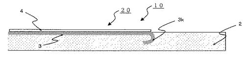
図11は、実施の形態4に係る多層セラミック基板10において、接続用導体パット20の端部を拡大した部分1の断面模式図である。図12は、実施の形態4による多層セラミック基板10の製造方法を示す断面模式図である。図11において、導体部3の端部から延長された導体延長部3kは、セラミック層2の内部でU字形状に折り返して、接続用導体パット導体3の直下に埋没している。
FIG. 11 is a schematic cross-sectional view of a
次に、図12に示す多層セラミック基板10の製造方法について説明する。図5のフローチャートの一部であるパターン印刷工程(ステップS3)および積層プレス工程(ステップS4)において、図12に示す実施の形態4の工程が行われる。
Next, a method for manufacturing the multilayer
図12(a)において、図示しない穴あけとVIA充填されたグリーンシート5の上に、まず導体ペースト6により導体延長部3kの形成前の導体3k−1を印刷する。
次に、図12(b)において、セラミックペースト7を、導体3k−1を囲むようにグリーンシート5上に印刷する。
In FIG. 12A, the
Next, in FIG.12 (b), the
次いで、図12(b)において、セラミックペースト7上に、導体ペースト6を印刷する。このとき、導体3k−1を同時に印刷する。その後、積層工程にて、上面に表面の平坦なプレート8を乗せてプレスする。
Next, in FIG. 12B, the
続いて、図12(c)において、セラミックペースト7とグリーンシート5は焼成工程にて一体化し、セラミック層2となる。かくして、図11に示すように、導体延長部3kは、U字形状に湾曲してセラミック層に埋没した形状となる。
Subsequently, in FIG. 12 (c), the
このように実施の形態4に係る多層セラミック基板10およびその製造方法は、導体延長部3kが、セラミック層2の内部でU字形状に屈曲しても良い。これにより、接続用導体パット20の密着性を向上させ、導体部3の形成する導体パットについて、剥離が生じることはない。これにより多層セラミック基板10を用いた高周波回路基板の品質がより安定する。
Thus, in the multilayer
実施の形態5.
図13は、実施の形態5に係る多層セラミック基板10において、接続用導体パット20の端部を拡大した部分1の断面模式図である。図13において、導体延長部3lは、接続用導体パット20の導体部3の端部から延長され、下方に向かってセラミック層2の内部に埋没している。即ち、導体延長部3lは、導体部3から垂直にパット下方に延長している。
FIG. 13 is a schematic cross-sectional view of a
次に、図6に示す多層セラミック基板10の製造方法について説明する。実施の形態5では、図5のフローチャートの穴あけ工程(ステップS1)にて、延長部となるVIA穴を開ける。次いで、VIA充填工程(ステップS2)にて延長部となるVIA穴に導体を形成する。
Next, a method for manufacturing the multilayer
その後、パターン印刷工程(ステップS3)において、導体パターンを印刷し、導体部3を形成する。その際、接続用導体パット20とその延長部である導体延長部3lとが、接続される。更に、積層工程(ステップS4)にて、上面に表面の平坦なプレート8を乗せてプレスした後、焼成後は導体延長部3lがセラミック基板に埋没した形状となる。
Then, in a pattern printing process (step S3), a conductor pattern is printed and the
以上、実施の形態5では、上述した製造工程を経ることによって、セラミック基板の内部に、VIA導体として埋没した導体延長部3lを持つ所望の接続用導体パット20が形成されるので、それらのアンカー効果により、密着性が向上する。
As described above, in the fifth embodiment, the desired connecting
2 セラミック層、3 導体部、3a〜3l 導体延長部、4 めっき層、5,5b グリーンシート、6 導体ペースト、7 セラミックペースト、8 金属プレート、10 多層セラミック基板、20 接続用導体パット。 2 ceramic layer, 3 conductor part, 3a-3l conductor extension part, 4 plating layer, 5, 5b green sheet, 6 conductor paste, 7 ceramic paste, 8 metal plate, 10 multilayer ceramic substrate, 20 conductor pad for connection.
Claims (4)
上記セラミック層の表面に形成された導体部、及び当該導体部の端部から延在した延長部からなる導体パットと、
を備え、
上記延長部が上記セラミック層の内部に形成された多層セラミック基板。 Ceramic layers stacked in multiple layers;
A conductor pad formed of a conductor portion formed on the surface of the ceramic layer, and an extension portion extending from an end portion of the conductor portion;
With
A multilayer ceramic substrate in which the extension is formed inside the ceramic layer.
上記印刷工程後、上記導体ペーストおよびセラミックペーストを押圧するプレス工程と、
上記プレス工程後、上記グリーンシートを焼成する焼成工程と、
を備えて、
セラミック層表面に形成される導体部の端部から延在する延長部を、当該セラミック層の内部に形成する多層セラミック基板の製造方法。 After printing the conductive paste on the laminated green sheets, a printing step of printing the ceramic paste facing the upper surface or peripheral edge of the conductive paste;
After the printing step, a pressing step for pressing the conductor paste and the ceramic paste,
A firing step of firing the green sheet after the pressing step;
With
The manufacturing method of the multilayer ceramic substrate which forms the extension part extended from the edge part of the conductor part formed in the ceramic layer surface inside the said ceramic layer.
Priority Applications (1)
| Application Number | Priority Date | Filing Date | Title |
|---|---|---|---|
| JP2012027045A JP2013165149A (en) | 2012-02-10 | 2012-02-10 | Multilayer ceramic substrate and manufacturing method of the same |
Applications Claiming Priority (1)
| Application Number | Priority Date | Filing Date | Title |
|---|---|---|---|
| JP2012027045A JP2013165149A (en) | 2012-02-10 | 2012-02-10 | Multilayer ceramic substrate and manufacturing method of the same |
Publications (1)
| Publication Number | Publication Date |
|---|---|
| JP2013165149A true JP2013165149A (en) | 2013-08-22 |
Family
ID=49176336
Family Applications (1)
| Application Number | Title | Priority Date | Filing Date |
|---|---|---|---|
| JP2012027045A Pending JP2013165149A (en) | 2012-02-10 | 2012-02-10 | Multilayer ceramic substrate and manufacturing method of the same |
Country Status (1)
| Country | Link |
|---|---|
| JP (1) | JP2013165149A (en) |
Cited By (2)
| Publication number | Priority date | Publication date | Assignee | Title |
|---|---|---|---|---|
| WO2017126596A1 (en) * | 2016-01-22 | 2017-07-27 | 京セラ株式会社 | Electronic component storage package, multi-piece wiring substrate, electronic device, and electronic module |
| JP7069222B2 (en) | 2018-01-24 | 2022-05-17 | 京セラ株式会社 | Wiring boards, electronic devices and electronic modules |
Citations (1)
| Publication number | Priority date | Publication date | Assignee | Title |
|---|---|---|---|---|
| JP2004104091A (en) * | 2002-07-16 | 2004-04-02 | Murata Mfg Co Ltd | Laminated ceramic electronic component and its manufacturing method |
-
2012
- 2012-02-10 JP JP2012027045A patent/JP2013165149A/en active Pending
Patent Citations (1)
| Publication number | Priority date | Publication date | Assignee | Title |
|---|---|---|---|---|
| JP2004104091A (en) * | 2002-07-16 | 2004-04-02 | Murata Mfg Co Ltd | Laminated ceramic electronic component and its manufacturing method |
Cited By (9)
| Publication number | Priority date | Publication date | Assignee | Title |
|---|---|---|---|---|
| WO2017126596A1 (en) * | 2016-01-22 | 2017-07-27 | 京セラ株式会社 | Electronic component storage package, multi-piece wiring substrate, electronic device, and electronic module |
| CN107534024A (en) * | 2016-01-22 | 2018-01-02 | 京瓷株式会社 | Electronic unit storage packaging body, more circuit board, electronic installation and electronic module in flakes |
| JPWO2017126596A1 (en) * | 2016-01-22 | 2018-03-15 | 京セラ株式会社 | Electronic component storage package, multi-cavity wiring board, electronic device and electronic module |
| EP3349244A4 (en) * | 2016-01-22 | 2018-09-26 | KYOCERA Corporation | Electronic component storage package, multi-piece wiring substrate, electronic device, and electronic module |
| CN107534024B (en) * | 2016-01-22 | 2018-10-26 | 京瓷株式会社 | Electronic unit storage packaging body, mostly circuit board, electronic device and electronic module in flakes |
| US10381281B2 (en) | 2016-01-22 | 2019-08-13 | Kyocera Corporation | Electronic component housing package, multi-piece wiring substrate, electronic apparatus, and electronic module having curved connection conductors |
| US10832980B2 (en) | 2016-01-22 | 2020-11-10 | Kyocera Corporation | Electronic component housing package, multi-piece wiring substrate, electronic apparatus, and electronic module |
| JP7069222B2 (en) | 2018-01-24 | 2022-05-17 | 京セラ株式会社 | Wiring boards, electronic devices and electronic modules |
| US11388819B2 (en) | 2018-01-24 | 2022-07-12 | Kyocera Corporation | Wiring board, electronic device, and electronic module |
Similar Documents
| Publication | Publication Date | Title |
|---|---|---|
| JP4341588B2 (en) | Multilayer substrate and manufacturing method thereof | |
| JP5700241B2 (en) | Multilayer wiring board and manufacturing method thereof | |
| JP6103054B2 (en) | Manufacturing method of resin multilayer substrate | |
| JP2012191204A (en) | Manufacturing method of printed wiring board | |
| TWI622332B (en) | Rigid and flexible composite circuit board | |
| JP4460341B2 (en) | Wiring board and manufacturing method thereof | |
| WO2012128269A1 (en) | Wiring substrate | |
| JP2008091874A (en) | Ceramic circuit substrate and method for manufacturing the same | |
| JP2019021863A (en) | Multilayer substrate | |
| JP2013165149A (en) | Multilayer ceramic substrate and manufacturing method of the same | |
| JP4597561B2 (en) | Wiring board and manufacturing method thereof | |
| JP4759041B2 (en) | Electronic component built-in multilayer board | |
| JP6536751B2 (en) | Laminated coil and method of manufacturing the same | |
| US9936575B2 (en) | Resin multilayer substrate and component module | |
| JP4550774B2 (en) | Wiring board built-in capacitor, wiring board, laminated body, capacitor assembly, wiring board built-in capacitor manufacturing method | |
| JP2013145847A (en) | Printed wiring board and manufacturing method of the same | |
| JP5516830B2 (en) | Component built-in resin substrate | |
| JP2015159242A (en) | Wiring board, and multilayer wiring board including the same | |
| JP5690892B2 (en) | Coreless multilayer wiring board and manufacturing method thereof | |
| JP2004111769A (en) | Electronic component mounting board | |
| JP2013191678A (en) | Multilayer wiring board | |
| WO2013008592A1 (en) | Wiring board | |
| JPH06252558A (en) | Multilayered glass ceramic cavity substrate | |
| WO2020203724A1 (en) | Resin multilayer substrate and method for producing resin multilayer substrate | |
| JP2006344631A (en) | Component built-in substrate |
Legal Events
| Date | Code | Title | Description |
|---|---|---|---|
| RD01 | Notification of change of attorney |
Free format text: JAPANESE INTERMEDIATE CODE: A7421 Effective date: 20140326 |
|
| A621 | Written request for application examination |
Free format text: JAPANESE INTERMEDIATE CODE: A621 Effective date: 20140417 |
|
| A131 | Notification of reasons for refusal |
Free format text: JAPANESE INTERMEDIATE CODE: A131 Effective date: 20141111 |
|
| A02 | Decision of refusal |
Free format text: JAPANESE INTERMEDIATE CODE: A02 Effective date: 20150324 |