JP2013074635A - Dc-dc converter - Google Patents
Dc-dc converter Download PDFInfo
- Publication number
- JP2013074635A JP2013074635A JP2011209702A JP2011209702A JP2013074635A JP 2013074635 A JP2013074635 A JP 2013074635A JP 2011209702 A JP2011209702 A JP 2011209702A JP 2011209702 A JP2011209702 A JP 2011209702A JP 2013074635 A JP2013074635 A JP 2013074635A
- Authority
- JP
- Japan
- Prior art keywords
- voltage
- converter
- duty
- rectangular wave
- current
- Prior art date
- Legal status (The legal status is an assumption and is not a legal conclusion. Google has not performed a legal analysis and makes no representation as to the accuracy of the status listed.)
- Withdrawn
Links
Images


Classifications
-
- H—ELECTRICITY
- H02—GENERATION; CONVERSION OR DISTRIBUTION OF ELECTRIC POWER
- H02M—APPARATUS FOR CONVERSION BETWEEN AC AND AC, BETWEEN AC AND DC, OR BETWEEN DC AND DC, AND FOR USE WITH MAINS OR SIMILAR POWER SUPPLY SYSTEMS; CONVERSION OF DC OR AC INPUT POWER INTO SURGE OUTPUT POWER; CONTROL OR REGULATION THEREOF
- H02M3/00—Conversion of DC power input into DC power output
- H02M3/02—Conversion of DC power input into DC power output without intermediate conversion into AC
- H02M3/04—Conversion of DC power input into DC power output without intermediate conversion into AC by static converters
- H02M3/10—Conversion of DC power input into DC power output without intermediate conversion into AC by static converters using discharge tubes with control electrode or semiconductor devices with control electrode
- H02M3/145—Conversion of DC power input into DC power output without intermediate conversion into AC by static converters using discharge tubes with control electrode or semiconductor devices with control electrode using devices of a triode or transistor type requiring continuous application of a control signal
- H02M3/155—Conversion of DC power input into DC power output without intermediate conversion into AC by static converters using discharge tubes with control electrode or semiconductor devices with control electrode using devices of a triode or transistor type requiring continuous application of a control signal using semiconductor devices only
- H02M3/156—Conversion of DC power input into DC power output without intermediate conversion into AC by static converters using discharge tubes with control electrode or semiconductor devices with control electrode using devices of a triode or transistor type requiring continuous application of a control signal using semiconductor devices only with automatic control of output voltage or current, e.g. switching regulators
- H02M3/158—Conversion of DC power input into DC power output without intermediate conversion into AC by static converters using discharge tubes with control electrode or semiconductor devices with control electrode using devices of a triode or transistor type requiring continuous application of a control signal using semiconductor devices only with automatic control of output voltage or current, e.g. switching regulators including plural semiconductor devices as final control devices for a single load
- H02M3/1588—Conversion of DC power input into DC power output without intermediate conversion into AC by static converters using discharge tubes with control electrode or semiconductor devices with control electrode using devices of a triode or transistor type requiring continuous application of a control signal using semiconductor devices only with automatic control of output voltage or current, e.g. switching regulators including plural semiconductor devices as final control devices for a single load comprising at least one synchronous rectifier element
-
- H—ELECTRICITY
- H02—GENERATION; CONVERSION OR DISTRIBUTION OF ELECTRIC POWER
- H02M—APPARATUS FOR CONVERSION BETWEEN AC AND AC, BETWEEN AC AND DC, OR BETWEEN DC AND DC, AND FOR USE WITH MAINS OR SIMILAR POWER SUPPLY SYSTEMS; CONVERSION OF DC OR AC INPUT POWER INTO SURGE OUTPUT POWER; CONTROL OR REGULATION THEREOF
- H02M3/00—Conversion of DC power input into DC power output
- H02M3/02—Conversion of DC power input into DC power output without intermediate conversion into AC
- H02M3/04—Conversion of DC power input into DC power output without intermediate conversion into AC by static converters
- H02M3/10—Conversion of DC power input into DC power output without intermediate conversion into AC by static converters using discharge tubes with control electrode or semiconductor devices with control electrode
- H02M3/145—Conversion of DC power input into DC power output without intermediate conversion into AC by static converters using discharge tubes with control electrode or semiconductor devices with control electrode using devices of a triode or transistor type requiring continuous application of a control signal
- H02M3/155—Conversion of DC power input into DC power output without intermediate conversion into AC by static converters using discharge tubes with control electrode or semiconductor devices with control electrode using devices of a triode or transistor type requiring continuous application of a control signal using semiconductor devices only
- H02M3/156—Conversion of DC power input into DC power output without intermediate conversion into AC by static converters using discharge tubes with control electrode or semiconductor devices with control electrode using devices of a triode or transistor type requiring continuous application of a control signal using semiconductor devices only with automatic control of output voltage or current, e.g. switching regulators
- H02M3/158—Conversion of DC power input into DC power output without intermediate conversion into AC by static converters using discharge tubes with control electrode or semiconductor devices with control electrode using devices of a triode or transistor type requiring continuous application of a control signal using semiconductor devices only with automatic control of output voltage or current, e.g. switching regulators including plural semiconductor devices as final control devices for a single load
- H02M3/1584—Conversion of DC power input into DC power output without intermediate conversion into AC by static converters using discharge tubes with control electrode or semiconductor devices with control electrode using devices of a triode or transistor type requiring continuous application of a control signal using semiconductor devices only with automatic control of output voltage or current, e.g. switching regulators including plural semiconductor devices as final control devices for a single load with a plurality of power processing stages connected in parallel
-
- H—ELECTRICITY
- H02—GENERATION; CONVERSION OR DISTRIBUTION OF ELECTRIC POWER
- H02M—APPARATUS FOR CONVERSION BETWEEN AC AND AC, BETWEEN AC AND DC, OR BETWEEN DC AND DC, AND FOR USE WITH MAINS OR SIMILAR POWER SUPPLY SYSTEMS; CONVERSION OF DC OR AC INPUT POWER INTO SURGE OUTPUT POWER; CONTROL OR REGULATION THEREOF
- H02M1/00—Details of apparatus for conversion
- H02M1/0003—Details of control, feedback or regulation circuits
-
- Y—GENERAL TAGGING OF NEW TECHNOLOGICAL DEVELOPMENTS; GENERAL TAGGING OF CROSS-SECTIONAL TECHNOLOGIES SPANNING OVER SEVERAL SECTIONS OF THE IPC; TECHNICAL SUBJECTS COVERED BY FORMER USPC CROSS-REFERENCE ART COLLECTIONS [XRACs] AND DIGESTS
- Y02—TECHNOLOGIES OR APPLICATIONS FOR MITIGATION OR ADAPTATION AGAINST CLIMATE CHANGE
- Y02B—CLIMATE CHANGE MITIGATION TECHNOLOGIES RELATED TO BUILDINGS, e.g. HOUSING, HOUSE APPLIANCES OR RELATED END-USER APPLICATIONS
- Y02B70/00—Technologies for an efficient end-user side electric power management and consumption
- Y02B70/10—Technologies improving the efficiency by using switched-mode power supplies [SMPS], i.e. efficient power electronics conversion e.g. power factor correction or reduction of losses in power supplies or efficient standby modes
Landscapes
- Engineering & Computer Science (AREA)
- Power Engineering (AREA)
- Dc-Dc Converters (AREA)
Abstract
【課題】複数のDC−DC変換部を均等に動作させて直流出力電圧を生成可能なDC−DCコンバータを提供する。
【解決手段】DC−DCコンバータは、直流入力電圧を矩形波電圧に変換する複数のDC−DC変換部と、複数のDC−DC変換部の出力端子に一端が接続され、他端が共通の外部出力端子に接続される複数のインダクタ素子と、複数のDC−DC変換部の出力端子にそれぞれ接続され、対応するDC−DC変換部から出力される矩形波電圧のデューティ比を検出する複数のデューティ検出回路と、複数のデューティ検出回路の出力信号を、2つずつ組にした各組ごとに比較した結果に基づいて、各組の矩形波電圧のデューティ比が等しくなるように、各組内の一方のデューティ検出回路に接続されたDC−DC変換部のデューティ比を調整するデューティ調整回路と、を備える。
【選択図】図1A DC-DC converter capable of generating a DC output voltage by operating a plurality of DC-DC converters equally.
A DC-DC converter includes a plurality of DC-DC converters that convert a DC input voltage into a rectangular wave voltage, and one end connected to the output terminals of the plurality of DC-DC converters, and the other end is common. A plurality of inductor elements connected to the external output terminal, and a plurality of inductors connected to the output terminals of the plurality of DC-DC converters, respectively, for detecting the duty ratio of the rectangular wave voltage output from the corresponding DC-DC converters Based on the results of comparing the output signals of the duty detection circuit and the plurality of duty detection circuits for each pair, so that the duty ratio of the rectangular wave voltage of each pair is equal, A duty adjustment circuit that adjusts the duty ratio of the DC-DC converter connected to one of the duty detection circuits.
[Selection] Figure 1
Description
本発明の実施形態は、複数のDC−DC変換部を用いてDC−DC変換を行うDC−DCコンバータに関する。 Embodiments described herein relate generally to a DC-DC converter that performs DC-DC conversion using a plurality of DC-DC conversion units.
最近の電子部品は、消費電力低減のために、低電圧で駆動するものが多い。この種の電子回路用の電源電圧を生成するために、DC−DCコンバータが用いられる。 Many recent electronic components are driven at a low voltage to reduce power consumption. A DC-DC converter is used to generate a power supply voltage for this type of electronic circuit.
DC−DCコンバータは、負荷に流せる電流量が予め決められており、それ以上の電流を流そうとすると、電源電圧レベルが下がるなどの所望の電気特性が得られなくなる。 In the DC-DC converter, the amount of current that can be passed through the load is determined in advance, and if it is attempted to pass more current, desired electrical characteristics such as a decrease in the power supply voltage level cannot be obtained.
電子回路の開発段階では、負荷の総容量を正確に見積もるのは困難であり、通常は、負荷容量にある程度の余裕を持たせて、それに対応するDC−DCコンバータを採用する。ところが、電子回路の開発の最終段階になって、先に見積もった負荷容量をわずかに超える場合がある。このような場合、DC−DCコンバータを大電流型に置換するのは時間的に困難な場合が少なくない。そこで、採用する予定だったDC−DCコンバータを余計に1つあるいは数個増やして、電流容量を増やす対策が取られることがある。 In the development stage of an electronic circuit, it is difficult to accurately estimate the total capacity of the load. Usually, a certain amount of margin is provided for the load capacity, and a corresponding DC-DC converter is employed. However, in the final stage of electronic circuit development, the load capacity estimated previously may be slightly exceeded. In such a case, it is often difficult to replace the DC-DC converter with a large current type in terms of time. Therefore, a measure may be taken to increase the current capacity by adding one or several additional DC-DC converters that were to be employed.
ところが、複数のDC−DCコンバータを電源ラインに並列接続すると、理想的には、個々のDC−DCコンバータが均等に動作するはずであるが、実際には、DC−DCコンバータ内の電子部品のばらつきによって、一部のDC−DCコンバータだけが偏って動作することがある。このため、大容量負荷への電流供給を複数のDC−DCコンバータで分散して行うことができず、負荷側の電子回路の電源電圧が低下するなどの不具合が生じてしまう。 However, when a plurality of DC-DC converters are connected in parallel to the power supply line, ideally, the individual DC-DC converters should operate equally, but in practice, the electronic components in the DC-DC converters Due to the variation, only some DC-DC converters may operate in a biased manner. For this reason, current supply to a large-capacity load cannot be performed by a plurality of DC-DC converters in a distributed manner, resulting in problems such as a decrease in power supply voltage of an electronic circuit on the load side.
本発明は、複数のDC−DC変換部を均等に動作させて直流出力電圧を生成可能なDC−DCコンバータを提供するものである。 The present invention provides a DC-DC converter capable of generating a DC output voltage by operating a plurality of DC-DC converters equally.
本発明の一態様では、矩形波電圧を出力する複数のDC−DC変換部と、
前記複数のDC−DC変換部のそれぞれに対応して一つずつ設けられ、対応するDC−DC変換部の出力端子に一端が接続され、他端が共通の外部出力端子に接続される複数のインダクタ素子と、
前記複数のDC−DC変換部の出力端子にそれぞれ一つずつ接続され、対応するDC−DC変換部から出力される矩形波電圧のデューティ比を検出する複数のデューティ検出回路と、
前記複数のデューティ検出回路の出力信号を、2つずつ組にした各組ごとに比較した結果に基づいて、各組の矩形波電圧のデューティ比が等しくなるように、各組内の一方のデューティ検出回路に接続されたDC−DC変換部のデューティ比を調整するデューティ調整回路と、を備えるDC−DCコンバータが提供される。
In one aspect of the present invention, a plurality of DC-DC converters that output a rectangular wave voltage;
One corresponding to each of the plurality of DC-DC converters, one end connected to the output terminal of the corresponding DC-DC converter, and the other end connected to a common external output terminal An inductor element;
A plurality of duty detection circuits connected to the output terminals of the plurality of DC-DC conversion units one by one and detecting the duty ratio of the rectangular wave voltage output from the corresponding DC-DC conversion unit;
Based on the result of comparing the output signals of the plurality of duty detection circuits in groups of two, one duty in each group is set so that the duty ratio of the rectangular wave voltage of each group becomes equal A DC-DC converter is provided that includes a duty adjustment circuit that adjusts a duty ratio of a DC-DC conversion unit connected to a detection circuit.
以下、図面を参照しながら、本発明の実施形態を説明する。 Hereinafter, embodiments of the present invention will be described with reference to the drawings.
(第1の実施形態)
図1は第1の実施形態に係るDC−DCコンバータ1の概略構成を示すブロック図である。図1のDC−DCコンバータ1は、2つのDC−DC変換部2a,2bを並列接続して、両DC−DC変換部2a,2bのデューティ比が略等しくなるように制御するものである。
(First embodiment)
FIG. 1 is a block diagram showing a schematic configuration of a DC-
より具体的には、図1のDC−DCコンバータ1は、2つのDC−DC変換部2a,2bと、各DC−DC変換部2a,2bの出力端子に接続されたTon検出回路3a,3bと、両Ton検出回路3a,3bの出力電圧の差電圧を検出する差動アンプ4と、差動アンプ4の出力電圧を検波および平均化する検波平均化回路5と、検波平均化回路5の出力電圧を電流信号に変換する電圧−電流変換器6とを備えている。
More specifically, the DC-
各DC−DC変換部2a,2bの出力端子にはコイルLa,Lbの一端が接続されており、コイルLa,Lbの他端はいずれもDC−DCコンバータ1の出力端子OUTに接続されている。各DC−DC変換部2a,2bは、直流入力電圧を矩形波電圧に変換する。矩形波電圧のデューティ比は、直流電流電圧の電圧レベルに応じて変化する。これら矩形波電圧は、コイルLa,Lbを介することにより、直流出力電圧Voutに変換されて出力端子OUTから出力される。
One ends of the coils La and Lb are connected to the output terminals of the DC-
出力端子OUTの出力電圧Voutは、各DC−DCコンバータ1の帰還端子FB1、FB2に帰還される。より具体的には、帰還端子FB1の電圧VRB1は、直流出力電圧Voutを抵抗素子R1,R2で抵抗分圧した電圧(=Vout・R2/(R1+R2))であり、帰還端子FB2の電圧VRB2は、直流出力電圧Voutを抵抗素子R3,R4,R5で抵抗分圧した電圧(=Vout・(R4+R5)/(R3+R4+R5))である。
The output voltage Vout of the output terminal OUT is fed back to the feedback terminals FB1 and FB2 of each DC-
本実施形態では、抵抗素子R4とR5を合算した抵抗値が抵抗素子R2の抵抗値よりも大きくなるようにしている。その理由については、後に詳述するが、電圧−電流変換器6の構成を簡略化するためである。
In the present embodiment, the total resistance value of the resistance elements R4 and R5 is set to be larger than the resistance value of the resistance element R2. The reason for this will be described in detail later, but this is to simplify the configuration of the voltage-
Ton検出回路3a,3bは、対応するDC−DC変換部2a,2bの出力電圧により、DC−DC変換部2a,2bのデューティ比を検出する。
The
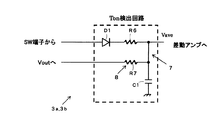
図2はTon検出回路3a,3bの内部構成の一例を示す回路図である。図2のTon検出回路3a,3bは、DC−DC変換部2aまたは2bの出力端子に接続されるダイオードD1と、ダイオードD1のカソード端子に接続される積分回路7と、積分回路7に接続される放電回路8とを有する。
FIG. 2 is a circuit diagram showing an example of the internal configuration of the
積分回路7は、ダイオードD1のカソード端子と差動アンプ4の入力端子との間に接続される抵抗素子R6と、差動アンプ4の入力端子と接地端子との間に接続されるコンデンサC1とを有する。放電回路8は、DC−DCコンバータ1の出力端子と差動アンプ4の入力端子との間に接続される抵抗素子R7を有する。
The integrating circuit 7 includes a resistance element R6 connected between the cathode terminal of the diode D1 and the input terminal of the
ダイオードD1は、DC−DC変換部2a,2bの出力信号が所定の閾値電圧を超える場合に、その信号を通過させて、積分回路7で電圧の平均化処理を行う。また、DC−DCコンバータ1の出力電圧がゼロになると、コンデンサC1の蓄積電荷を放電回路8を介して放電する。
When the output signals of the DC-
図3は検波平均化回路5および電圧−電流変換器6の内部構成の一例を示す回路図である。図3の検波平均化回路5は、差動アンプ4の出力端子に接続されるダイオードD2と、ダイオードD2のカソード端子に接続される積分回路9と、この積分回路9に接続される放電回路10とを有する。電圧−電流変換器6は、放電回路10に接続されている。
FIG. 3 is a circuit diagram showing an example of the internal configuration of the detection averaging
積分回路9は、ダイオードD2のカソード端子と接地端子との間に直列接続される抵抗素子R8およびコンデンサC2を有する。放電回路10は、コンデンサC2に並列接続される抵抗素子R9を有する。
The integration circuit 9 includes a resistance element R8 and a capacitor C2 connected in series between the cathode terminal of the diode D2 and the ground terminal. The
電圧−電流変換器6は、DC−DC変換部2a,2bの帰還端子FB2と接地端子の間に直列接続されるNchMOSトランジスタQ3および抵抗素子R10を有する。
The voltage-
ダイオードD2、積分回路9および放電抵抗R9は、差動アンプ4の出力電圧を検波および平均化し、NchMOSトランジスタQ3と抵抗素子R10は、検波および平均化した電圧を電流信号に変換する。
Diode D2, integrating circuit 9, and discharge resistor R9 detect and average the output voltage of
次に、DC−DC変換部2a,2bの内部構成について説明する。2つのDC−DC変換部2a,2bは、いずれも共通した内部構成を有し、エラーアンプ11と、三角波発振器12と、パルス幅変調器13と、プレドライバ14と、ハイサイド側トランジスタQ1と、ロウサイド側トランジスタQ2とを有する。
Next, the internal configuration of the DC-
エラーアンプ11は、帰還電圧VFB1またはVFB2を、基準電圧Vref1またはVref2と比較して、電圧差に応じたエラー信号を出力する。パルス幅変調器13は、エラー信号を三角波発振器12の出力電圧と比較して、パルス幅変調信号を出力する。プレドライバ14は、パルス幅変調信号に基づいて、ハイサイド側トランジスタQ1とロウサイド側トランジスタQ2を切替制御して、出力信号である矩形波電圧のデューティ比を調整する。
The
図4はDC−DC変換部2a,2bから出力される矩形波電圧波形の一例を示す波形図である。図4では、DC−DC変換部2a,2bから出力される矩形波電圧がハイレベルのときをTon期間、ロウレベルのときをToff期間と呼んでおり、Ton/(Ton+Toff=T)がデューティ比である。
FIG. 4 is a waveform diagram showing an example of a rectangular wave voltage waveform output from the DC-
図4からわかるように、TonからToffに移行するときに、いったん電圧が落ち込んでいる。この期間はデッド期間と呼ばれるものであり、ハイサイド側トランジスタQ1とロウサイド側トランジスタQ2の双方がオフの期間である。デッド期間を設ける理由は、TonからToff、あるいはToffからTonに切り替わるときに、ハイサイド側トランジスタQ1とロウサイド側トランジスタQ2の双方がオンして貫通電流が流れるのを防止するためである。 As can be seen from FIG. 4, the voltage once drops when transitioning from Ton to Toff. This period is called a dead period, and both the high-side transistor Q1 and the low-side transistor Q2 are off. The reason for providing the dead period is to prevent both the high-side transistor Q1 and the low-side transistor Q2 from turning on and causing a through current to flow when switching from Ton to Toff or from Toff to Ton.
次に、図1のDC−DCコンバータ1の動作を説明する。各DC−DC変換部2a,2bの出力信号は、対応するTon検出回路3a,3bに入力されて、この出力信号のデューティ比が検出される。より具体的には、Ton検出回路3a,3bは、DC−DC変換部2a,2bの出力信号のデューティ比に応じた電圧レベルを持つ電圧信号を出力する。
Next, the operation of the DC-
そして、差動アンプ4は、これら2つのTon検出回路3a,3bの出力信号の電圧レベルを比較して、電圧差に応じた信号を出力する。差動アンプ4の出力信号は、検波平均化回路5で電圧レベルが平均化された後、電圧−電流変換器6で電流信号に変換される。したがって、電圧−電流変換器6は、両DC−DC変換部2a,2bのデューティ比の差に応じた電流信号を出力することになる。
Then, the
電圧−電流変換器6から出力された電流信号は、DC−DC変換部2bの帰還端子FB2に接続された抵抗素子R4,R5に流れる。これにより、帰還電圧VFB2の電圧レベルは、DC−DC変換部2bのデューティ比がDC−DC変換部2aのデューティ比より大きいほど、高くなる。
The current signal output from the voltage-
エラーアンプ11は、帰還電圧VFB1,VFB2と基準電圧Vref1,Vref2との電圧差に応じた信号を出力する。したがって、DC−DC変換部2b内のエラーアンプ11は、DC−DC変換部2bのデューティ比がDC−DC変換部2aのデューティ比より大きいほど、小さい電圧レベルの信号を出力する。
The
パルス幅変調器13は、エラーアンプ11の出力電圧レベルが大きいほど、パルス幅の広いパルス幅変調信号をプレドライバ14に供給する。よって、両DC−DC変換部2a,2bのデューティ比の差に応じて、ハイサイド側トランジスタQ1とロウサイド側トランジスタQ2のオン/オフ期間が調整されて、矩形波電圧が生成されることになる。
The
例えば、DC−DC変換部2bに接続されたTon検出回路3bで検出されたデューティ比が、DC−DC変換部2aに接続されたTon検出回路3aで検出されたデューティ比よりも大きかったとする。この場合、差動アンプ4の出力電圧レベルは大きくなり、電圧−電流変換器6から出力される電流信号の振幅も大きくなる。よって、帰還端子FB2に接続された抵抗素子R4,R5の両端電圧VFB2がより大きくなり、エラーアンプ11の出力電圧レベルは低くなる。よって、ハイサイド側トランジスタQ1のオン期間が短くなるように制御され、矩形波電圧のデューティ比が小さくなる。
For example, it is assumed that the duty ratio detected by the
このような制御により、2つのDC−DC変換部2a,2bのデューティ比は互いに等しくなるように、帰還制御される。
By such control, feedback control is performed so that the duty ratios of the two DC-
本実施形態では、DC−DC変換部2bの帰還端子FB2に接続された抵抗素子R4とR5を合算した抵抗値を、DC−DC変換部2aの帰還端子FB1に接続された抵抗素子R2の抵抗値よりも大きくしている。これにより、電圧−電流変換器6からの電流が抵抗素子R4とR5を通って接地端子に流れることになり、抵抗素子R4とR5の両端電圧差が帰還電圧VFB2になる。すなわち、抵抗素子R4とR5を合算した抵抗値を抵抗素子R2の抵抗値よりも大きくすることで、電圧−電流変換器6からの電流が抵抗素子R4とR5に流れるようにオフセットを与えることになる。また、電圧−電流変換器6は、常に抵抗素子R4とR5に電流を流すようになり、外部からの電流を内部に引き込む動作は行わないため、電圧−電流変換器6の内部構成を簡略化できる。
In the present embodiment, the resistance value of the resistance elements R4 and R5 connected to the feedback terminal FB2 of the DC-
なお、DC−DC変換部2bの帰還端子FB2に接続された抵抗素子R4とR5を合算した抵抗値を、DC−DC変換部2aの帰還端子FB1に接続された抵抗素子R2の抵抗値よりも小さくしてもよい。この場合は、DC−DC変換部2bの出力端子からの電流が電圧−電流変換器6に流れ込むことになり、流れ込む電流の量は、両DC−DC変換部2a,2bのデューティ比の差に依存する。すなわち、電圧−電流変換器6は、外部からの電流を内部に引き込む動作のみを行うことにより、やはり電圧−電流変換器6の内部構成を簡略化できる。
The resistance value obtained by adding the resistance elements R4 and R5 connected to the feedback terminal FB2 of the DC-
このように、DC−DC変換部2bの帰還端子FB2に接続された抵抗素子R4とR5を合算した抵抗値を、DC−DC変換部2aの帰還端子FB1に接続された抵抗素子R2の抵抗値より大きくすれば、電圧−電流変換器6は電流を帰還端子FB2側に送り出す作用を行い、DC−DC変換部2bの帰還端子FB2に接続された抵抗素子R4とR5を合算した抵抗値を、DC−DC変換部2aの帰還端子FB1に接続された抵抗素子R2の抵抗値より小さくすれば、電圧−電流変換器6は電流を引き込む作用を行う。どちらにしても、両DC−DC変換部2a,2bのデューティ比が等しくなるような制御を行うことができる。
Thus, the resistance value of the resistance element R2 connected to the feedback terminal FB1 of the DC-
上述したように、第1の実施形態では、両DC−DC変換部2a,2bの出力端子にそれぞれTon検出回路3a,3bを設けて出力信号のデューティ比を検出し、デューティ比の差に応じた電流信号を帰還制御して、ハイサイド側トランジスタQ1とロウサイド側トランジスタQ2のオン/オフ期間を調整するため、両DC−DC変換部2a,2bのデューティ比を等しくすることができ、大容量負荷の駆動を、両DC−DC変換部2a,2bで均等に分担することができ、大容量負荷を駆動する場合であっても電源電圧レベルの安定化が図れる。
As described above, in the first embodiment, the
(第2の実施形態)
上述したTon検出回路3a,3bは、DC−DC変換部2a,2bの出力端子のデューティ比を検出するものであり、図2に示すように、ダイオードD1により、Ton期間のみ出力信号を通過させて、その通過信号の電圧平均化処理を行っている。これに対して、Toff期間のみ出力信号を通過させるような変形例も可能である。この場合、Ton検出回路3a,3bの代わりに、Toff検出回路21a,21bが設けられる。
(Second Embodiment)
The above-described
図5は第2の実施形態に係るDC−DCコンバータ1の概略構成を示すブロック図である。図5では、図1と共通する構成部分には同一符号を付しており、以下では相違点を中心に説明する。
FIG. 5 is a block diagram showing a schematic configuration of the DC-
図5のDC−DCコンバータ1は、各DC−DC変換部2a,2bの出力端子に接続されるToff検出回路21a,21bを有する。Toff検出回路21a,21bは、DC−DC変換部2a,2bの出力信号が所定電圧レベル以下の期間内に、その出力信号の平均電圧を検出する。これにより、結果として、Toff検出回路21a,21bは、図2のTon検出回路3a,3bと同様に、デューティ比を検出する。
The DC-
図6はToff検出回路21a,21bの内部構成の一例を示す回路図である。図6のToff検出回路21a,21bは、図2のTon検出回路3a,3bと比べて、ダイオードD1の接続の向きが異なっており、その他の構成は共通である。
FIG. 6 is a circuit diagram showing an example of the internal configuration of the
図6のToff検出回路21a,21bでは、DC−DC変換部2a,2bの出力端子にダイオードのカソード端子が接続されているため、DC−DC変換部2a,2bの出力信号が所定電圧レベル以下の場合に、ダイオードはその信号を通過させて、平均化処理を行う。
In the
図7は図5のDC−DCコンバータ1内の差動アンプ4の出力端子に接続される検波平均化回路5と電圧−電流変換器6の内部構成を示す回路図である。図7の検波平均化回路5は、ダイオードD2と、積分回路9と、充電回路22とを有する。図7の検波平均化回路5を図3の検波平均化回路5と比較すると、ダイオードD2の接続の向きが異なることと、放電回路10の代わりに充電回路22が接続されていることとが異なる。充電回路22は、電源端子と積分回路9の出力端子との間に接続される抵抗素子R9を有する。
FIG. 7 is a circuit diagram showing the internal configuration of the
また、図7の電圧−電流変換器6は、電源端子と帰還端子FB2との間に直列接続される抵抗素子R10とPchMOSトランジスタQ4とを有する。図7の電圧−電流変換器6を図3の電圧−電流変換器6と比較すると、抵抗素子R10が接地端子ではなく電源端子に接続され、かつ、トランジスタQ4の導電型がP型であることが異なる。
7 includes a resistance element R10 and a PchMOS transistor Q4 connected in series between the power supply terminal and the feedback terminal FB2. When the voltage-
このように、第2の実施形態では、各DC−DC変換部2a,2bの出力端子にToff検出回路21a,21bを接続して、デューティ比を検出するため、Ton検出回路3a,3bを接続した場合と同様に、両DC−DC変換部2a,2bのデューティ比が等しくなるような制御が可能となる。
Thus, in the second embodiment, the
(第3の実施形態)
第3の実施形態は、差動アンプ4、検波平均化回路5および電圧−電流変換器6を統合するものである。
(Third embodiment)
In the third embodiment, the
図8は第3の実施形態に係るDC−DCコンバータ1の内部構成を示すブロック図である。図8では、図1や図5と共通する構成部分には同一符号を付しており、以下では相違点を説明する。
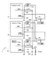
FIG. 8 is a block diagram showing an internal configuration of the DC-
図8のDC−DCコンバータ1は、図1のDC−DCコンバータ1と比較して、Ton検出回路3a,3bの代わりに平均化回路23a,23bを有し、差動アンプ4、検波平均化回路5および電圧−電流変換器6を統合した電流出力アンプ24を有する点で異なる。
Compared with the DC-
図9は図8の平均化回路23a,23bの内部構成の一例を示すブロック図である。図9の平均化回路23a,23bは、図2のTon検出回路3a,3bからダイオードD1を削除した構成である。図9の平均化回路23a,23bは、対応するDC−DC変換部2a,2bの出力信号を、その電圧レベルに依存せずに平均化する処理を行う。
FIG. 9 is a block diagram showing an example of the internal configuration of the averaging
図8の電流出力アンプ24は、両平均化回路23a,23bの出力電圧差に応じた電流信号を生成する。これにより、電流出力アンプ24の出力電流波形は、図1の電圧−電流変換器6の出力電流波形と同様になる。
The
このように、第3の実施形態では、Ton検出回路3a,3bやToff検出回路21a,21bよりも回路構成を簡略化した平均化回路23a,23bを設け、かつ差動アンプ4、検波平均化回路5および電圧−電流変換器6を統合した電流出力アンプ24を有するため、DC−DCコンバータ1の回路規模を第1および第2の実施形態のDC−DCコンバータ1よりも簡略化できる。
As described above, in the third embodiment, the averaging
(第4の実施形態)
第1〜第3の実施形態では、DC−DCコンバータ1内に並列接続された2つのDC−DC変換部2a,2bを設ける例を説明したが、並列接続された3つ以上のDC−DC変換部をDC−DCコンバータ1内に設けてもよい。
(Fourth embodiment)
In the first to third embodiments, the example in which the two DC-
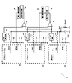
図10は第4の実施形態に係るDC−DCコンバータ1の概略構成を示すブロック図である。図10のDC−DCコンバータ1は、図1のDC−DCコンバータ1と比較して、3つのDC−DC変換部2a,2b,2cを備えるとともに、差動アンプ4、検波平均化回路5および電圧−電流変換器6を2つずつ備えている。また、電圧−電流変換器6の出力端子に接続されたDC−DC変換部2b,2cの帰還端子と、接地端子との間には、2つの抵抗素子R4,R5が直列接続されている。
FIG. 10 is a block diagram showing a schematic configuration of the DC-
差動アンプ4は、DC−DC変換部2aに接続されたTon検出回路3aの出力電圧を基準として、残りの2つのDC−DC変換部2b,2cに接続されたTon検出回路3b,3cの出力電圧との間で、それぞれ電圧差を検出する。電圧−電流変換器6は、対応する差動アンプ4で検出された電圧差に応じた電流信号を、対応するDC−DC変換部2b,2c内の帰還端子に接続された抵抗素子R4,R5に供給する。
The
帰還端子FB2と接地端子の間に直列接続された2つの抵抗素子R4,R5の抵抗値の合計は、電圧−電流変換器6からの電流信号が帰還されない帰還端子FB1と接地端子の間に接続された抵抗素子R2の抵抗値よりも、大きく設定されている。これにより、第1の実施形態で説明したように、電圧−電流変換器6からの電流信号は、常に、直列接続された抵抗素子に引き込まれることになり、電圧−電流変換器6の構成を簡略化できる。
The sum of the resistance values of the two resistance elements R4 and R5 connected in series between the feedback terminal FB2 and the ground terminal is connected between the feedback terminal FB1 to which the current signal from the voltage-
なお、第1の実施形態で説明したように、帰還端子FB2と接地端子の間に直列接続された2つの抵抗素子R4,R5の抵抗値の合計を、電圧−電流変換器6からの電流信号が帰還されない帰還端子FB1と接地端子の間に接続された抵抗素子R2の抵抗値よりも小さく設定してもよい。この場合は、コイルLbと抵抗素子R3を通過した電流を電圧−電流変換器6に常に引き込むことになり、この場合も電圧−電流変換器6の構成を簡略化できる。
As described in the first embodiment, the total resistance value of the two resistance elements R4 and R5 connected in series between the feedback terminal FB2 and the ground terminal is used as a current signal from the voltage-
図11は図10の第1変形例に係るDC−DCコンバータ1の概略構成を示すブロック図である。図11のDC−DCコンバータ1は、差動アンプ4で比較を行う対象が図10と異なっている。図11の差動アンプ4は、隣り合うDC−DCコンバータ1に接続された2つのTon検出回路(3a,3b)または(3b,3c)の出力電圧同士を比較して、その電圧差を検出する。
FIG. 11 is a block diagram showing a schematic configuration of a DC-
図12は図10の第2変形例に係るDC−DCコンバータ1の概略構成を示すブロック図である。図12のDC−DCコンバータ1は、Ton検出回路3a,3b,3cの代わりに図9の平均化回路23a,23b,23cを備え、差動アンプ4、検波平均化回路5および電圧−電流変換器6を統合した電流出力アンプ24を備える点で、図10のDC−DCコンバータ1と異なっている。
FIG. 12 is a block diagram showing a schematic configuration of a DC-
図13は図10の第3変形例に係るDC−DCコンバータ1の概略構成を示すブロック図である。図13のDC−DCコンバータ1は、Ton検出回路3a,3b,3cの代わりに図9の平均化回路23a,23b,23cを備え、差動アンプ4、検波平均化回路5および電圧−電流変換器6を統合した電流出力アンプ24を備える点で、図11のDC−DCコンバータ1と異なっている。
FIG. 13 is a block diagram showing a schematic configuration of a DC-
このように、第4の実施形態では、DC−DC変換部2a,2b,2cを3つ備えている場合には、2つずつのDC−DC変換部のデューティ比を比較した結果をそれぞれ帰還制御することで、すべてのDC−DC変換部2a,2b,2cのデューティ比を一致させることができる。
As described above, in the fourth embodiment, when three DC-
DC−DC変換部がn個(nは2以上の整数)ある場合は、これらDC−DC変換部を2個ずつの(n−1)組に分けて、各組ごとに、差動アンプ4でデューティ比の差を検出して、帰還制御すればよい。
When there are n DC-DC conversion units (n is an integer of 2 or more), these DC-DC conversion units are divided into two (n-1) groups, and the
(第5の実施形態)
図1等では、差動アンプ4の出力端子に検波平均化回路5を接続し、その後段に電圧−電流変換器6を接続しているが、検波平均化回路5を省略してもよい。
(Fifth embodiment)
In FIG. 1 and the like, the
図14は第5の実施形態に係るDC−DCコンバータ1の概略構成を示すブロック図である。図14は差動アンプ4の出力端子に直接、電圧−電流変換器6が接続されている点で図1と異なっている。なお、図14は、図1のTon検出回路3a,3bの代わりに図9に内部構成を示した平均化回路23a,23bを備えているが、これは本質的な違いではなく、平均化回路23a,23bの代わりに、Ton検出回路3a,3bやToff検出回路21a,21bを接続してもよい。
FIG. 14 is a block diagram showing a schematic configuration of the DC-
図15は図14の電圧−電流変換器6の内部構成の一例を示す回路図である。図15の電圧−電流変換器6は、帰還端子FB2と接地端子の間に直列接続されたNPNトランジスタまたはNchMOSトランジスタQ3と、抵抗素子R10とを有する。
FIG. 15 is a circuit diagram showing an example of the internal configuration of the voltage-
図15のDC−DCコンバータ1は、検波平均化回路5がない分だけ図1よりも構成を簡略化でき、回路面積および部品コストの削減を図れる。
The configuration of the DC-
図16は図15の変形例であり、3つのDC−DC変換部2a,2b,2cを備えた例を示すブロック図である。図16のDC−DCコンバータ1は、差動アンプ4の出力端子に電圧−電流変換器6が直接接続されている点を除いて、図12のDC−DCコンバータ1と同様に構成されている。
FIG. 16 is a modification of FIG. 15 and is a block diagram showing an example provided with three DC-
図17は図13の変形例であり、差動アンプ4の出力端子に電圧−電流変換器6が直接接続されている点を除いて、図13のDC−DCコンバータ1と同様に構成されている。
FIG. 17 is a modification of FIG. 13 and is configured in the same manner as the DC-
このように、差動アンプ4の出力端子に電圧−電流変換器6を直接接続した場合であっても、各DC−DC変換部のデューティ比を一致させるための電流信号を生成できる。また、検波平均化回路5を省略することは、DC−DCコンバータ1内に設けられるDC−DC変換部の数が多いほど、回路面積削減の効果が大きくなる。
Thus, even when the voltage-
本発明の態様は、上述した個々の実施形態に限定されるものではなく、当業者が想到しうる種々の変形も含むものであり、本発明の効果も上述した内容に限定されない。すなわち、特許請求の範囲に規定された内容およびその均等物から導き出される本発明の概念的な思想と趣旨を逸脱しない範囲で種々の追加、変更および部分的削除が可能である。 The aspect of the present invention is not limited to the individual embodiments described above, and includes various modifications that can be conceived by those skilled in the art, and the effects of the present invention are not limited to the contents described above. That is, various additions, modifications, and partial deletions can be made without departing from the concept and spirit of the present invention derived from the contents defined in the claims and equivalents thereof.
1 DC−DCコンバータ
2a,2b,2c DC−DC変換部
3a,3b,3c Ton検出回路
4 差動アンプ
5 検波平均回路
6 電圧−電流変換器
7 積分回路
8 放電回路
11 エラーアンプ
12 三角波発振器
13 パルス幅変調器
14 プレドライバ
Q1 ハイサイド側トランジスタ
Q2 ロウサイド側トランジスタ
DESCRIPTION OF
Claims (6)
前記複数のDC−DC変換部のそれぞれに対応して一つずつ設けられ、対応するDC−DC変換部の出力端子に一端が接続され他端が共通の外部出力端子に接続される複数のインダクタ素子と、
前記複数のDC−DC変換部の出力端子にそれぞれ一つずつ接続され、対応するDC−DC変換部から出力される矩形波電圧のデューティ比を検出する複数のデューティ検出回路と、
前記複数のデューティ検出回路の出力信号を、2つずつ組にした各組ごとに比較した結果に基づいて、各組の矩形波電圧のデューティ比が等しくなるように、各組内の一方のデューティ検出回路に接続されたDC−DC変換部のデューティ比を調整するデューティ調整回路と、を備え、
前記複数のデューティ検出回路のそれぞれは、前記矩形波電圧が所定の電圧レベル以上の期間内の前記矩形波電圧の平均電圧の電圧レベル、あるいは、前記矩形波電圧が所定の電圧レベル未満の期間内の前記矩形波電圧の平均電圧の電圧レベルにより、前記デューティ比を検出し、
前記デューティ調整回路は、各組における2つのデューティ検出回路で検出された平均電圧同士の電圧差を電流信号に変換する電圧電流変換器を有し、
前記DC−DC変換部は、
前記矩形波電圧の分圧電圧を生成する分圧抵抗部と、
前記分圧電圧と基準電圧との電圧差に応じて前記矩形波電圧のデューティ比を制御するデューティ制御回路と、を有し、
前記電圧電流変換器に接続される前記DC−DC変換部内の前記分圧抵抗部は、前記電流信号に応じた前記分圧電圧を生成し、
各組内の一方のデューティ検出回路に接続された前記DC−DC変換部内の前記分圧抵抗部の抵抗値と、他方のデューティ検出回路に接続された前記DC−DC変換部内の前記分圧抵抗部の抵抗値とは異なり、
前記デューティ調整回路は、前記電圧電流変換器を内蔵する電流出力可能な差動増幅器であることを特徴とするDC−DCコンバータ。 A plurality of DC-DC converters for outputting a rectangular wave voltage;
A plurality of inductors provided one by one corresponding to each of the plurality of DC-DC converters, one end connected to the output terminal of the corresponding DC-DC converter, and the other end connected to a common external output terminal Elements,
A plurality of duty detection circuits connected to the output terminals of the plurality of DC-DC conversion units one by one and detecting the duty ratio of the rectangular wave voltage output from the corresponding DC-DC conversion unit;
Based on the result of comparing the output signals of the plurality of duty detection circuits in groups of two, one duty in each group is set so that the duty ratio of the rectangular wave voltage of each group becomes equal A duty adjustment circuit that adjusts the duty ratio of the DC-DC converter connected to the detection circuit,
Each of the plurality of duty detection circuits includes a voltage level of an average voltage of the rectangular wave voltage within a period in which the rectangular wave voltage is equal to or higher than a predetermined voltage level, or a period in which the rectangular wave voltage is less than a predetermined voltage level. The duty ratio is detected by the voltage level of the average voltage of the rectangular wave voltage of
The duty adjustment circuit has a voltage-current converter that converts a voltage difference between average voltages detected by two duty detection circuits in each group into a current signal,
The DC-DC converter is
A voltage dividing resistor for generating a divided voltage of the rectangular wave voltage;
A duty control circuit that controls a duty ratio of the rectangular wave voltage according to a voltage difference between the divided voltage and a reference voltage;
The voltage dividing resistor in the DC-DC converter connected to the voltage-current converter generates the divided voltage according to the current signal,
The resistance value of the voltage dividing resistor in the DC-DC converter connected to one duty detection circuit in each set, and the voltage dividing resistor in the DC-DC converter connected to the other duty detection circuit Unlike the resistance value of the
The DC-DC converter according to claim 1, wherein the duty adjustment circuit is a differential amplifier capable of outputting a current and incorporating the voltage-current converter.
前記複数のDC−DC変換部のそれぞれに対応して一つずつ設けられ、対応するDC−DC変換部の出力端子に一端が接続され、他端が共通の外部出力端子に接続される複数のインダクタ素子と、
前記複数のDC−DC変換部の出力端子にそれぞれ一つずつ接続され、対応するDC−DC変換部から出力される矩形波電圧のデューティ比を検出する複数のデューティ検出回路と、
前記複数のデューティ検出回路の出力信号を、2つずつ組にした各組ごとに比較した結果に基づいて、各組の矩形波電圧のデューティ比が等しくなるように、各組内の一方のデューティ検出回路に接続されたDC−DC変換部のデューティ比を調整するデューティ調整回路と、を備えることを特徴とするDC−DCコンバータ。 A plurality of DC-DC converters for outputting a rectangular wave voltage;
One corresponding to each of the plurality of DC-DC converters, one end connected to the output terminal of the corresponding DC-DC converter, and the other end connected to a common external output terminal An inductor element;
A plurality of duty detection circuits connected to the output terminals of the plurality of DC-DC conversion units one by one and detecting the duty ratio of the rectangular wave voltage output from the corresponding DC-DC conversion unit;
Based on the result of comparing the output signals of the plurality of duty detection circuits in groups of two, one duty in each group is set so that the duty ratio of the rectangular wave voltage of each group becomes equal A DC-DC converter comprising: a duty adjustment circuit that adjusts a duty ratio of a DC-DC conversion unit connected to the detection circuit.
前記DC−DC変換部は、
前記矩形波電圧の分圧電圧を生成する分圧抵抗部と、
前記分圧電圧と基準電圧との電圧差に応じて前記矩形波電圧のデューティ比を制御するデューティ制御回路と、を有し、
前記電圧電流変換器に接続される前記DC−DC変換部内の前記分圧抵抗部は、前記電流信号に応じた前記分圧電圧を生成することを特徴とする請求項3に記載のDC−DCコンバータ。 The duty adjustment circuit has a voltage-current converter that converts a voltage difference between average voltages detected by two duty detection circuits in each group into a current signal,
The DC-DC converter is
A voltage dividing resistor for generating a divided voltage of the rectangular wave voltage;
A duty control circuit that controls a duty ratio of the rectangular wave voltage according to a voltage difference between the divided voltage and a reference voltage;
The DC-DC according to claim 3, wherein the voltage dividing resistor in the DC-DC converter connected to the voltage-current converter generates the divided voltage according to the current signal. converter.
Priority Applications (3)
| Application Number | Priority Date | Filing Date | Title |
|---|---|---|---|
| JP2011209702A JP2013074635A (en) | 2011-09-26 | 2011-09-26 | Dc-dc converter |
| CN2012100528988A CN103023316A (en) | 2011-09-26 | 2012-03-02 | Dc-dc converter and dc-dc conversion method |
| US13/424,526 US8854021B2 (en) | 2011-09-26 | 2012-03-20 | DC-DC converter and DC-DC conversion method |
Applications Claiming Priority (1)
| Application Number | Priority Date | Filing Date | Title |
|---|---|---|---|
| JP2011209702A JP2013074635A (en) | 2011-09-26 | 2011-09-26 | Dc-dc converter |
Publications (1)
| Publication Number | Publication Date |
|---|---|
| JP2013074635A true JP2013074635A (en) | 2013-04-22 |
Family
ID=47910578
Family Applications (1)
| Application Number | Title | Priority Date | Filing Date |
|---|---|---|---|
| JP2011209702A Withdrawn JP2013074635A (en) | 2011-09-26 | 2011-09-26 | Dc-dc converter |
Country Status (3)
| Country | Link |
|---|---|
| US (1) | US8854021B2 (en) |
| JP (1) | JP2013074635A (en) |
| CN (1) | CN103023316A (en) |
Cited By (1)
| Publication number | Priority date | Publication date | Assignee | Title |
|---|---|---|---|---|
| JP2019534678A (en) * | 2016-10-03 | 2019-11-28 | 日本テキサス・インスツルメンツ合同会社 | Transition event detector circuit and method |
Families Citing this family (6)
| Publication number | Priority date | Publication date | Assignee | Title |
|---|---|---|---|---|
| CN104092372B (en) * | 2014-06-30 | 2017-04-12 | 成都芯源系统有限公司 | Switch regulating circuit and mean current detection circuit and method thereof |
| CN105281315A (en) * | 2014-07-24 | 2016-01-27 | 中兴通讯股份有限公司 | Power supply control device and method of communication network |
| US9502964B2 (en) | 2014-12-16 | 2016-11-22 | Intel Corporation | Systems and methods for skewing DC/DC converter phases to mitigate spurs |
| CN106160457B (en) * | 2015-04-17 | 2019-03-29 | 台达电子工业股份有限公司 | DC conversion device and operation method thereof |
| FR3082351B1 (en) * | 2018-06-08 | 2021-10-22 | Valeo Systemes De Controle Moteur | COMPONENT FORMING AT LEAST TWO INDUCTANCES |
| EP4152584A4 (en) * | 2020-06-29 | 2023-06-28 | Huawei Technologies Co., Ltd. | Multi-phase power supply and electronic device |
Family Cites Families (8)
| Publication number | Priority date | Publication date | Assignee | Title |
|---|---|---|---|---|
| US6897636B2 (en) * | 2002-03-29 | 2005-05-24 | Intersil Americas Inc. | Method and circuit for scaling and balancing input and output currents in a multi-phase DC-DC converter using different input voltages |
| TW538586B (en) * | 2002-05-27 | 2003-06-21 | Richtek Technology Corp | Two-step ripple-free multi-phase converter and the converting method thereof |
| US6989657B2 (en) * | 2003-02-03 | 2006-01-24 | Jam Technologies, Llc | Method of detecting switching power supply output current |
| US7506179B2 (en) * | 2003-04-11 | 2009-03-17 | Zilker Labs, Inc. | Method and apparatus for improved DC power delivery management and configuration |
| JP4229177B2 (en) * | 2006-11-30 | 2009-02-25 | ミツミ電機株式会社 | Multi-phase DC-DC converter |
| JP5112111B2 (en) | 2008-03-04 | 2013-01-09 | 株式会社ダイヘン | DC power supply and grid-connected inverter system using this DC power supply |
| US8120203B2 (en) * | 2008-07-18 | 2012-02-21 | Intersil Americas Inc. | Intelligent management of current sharing group |
| JP5293155B2 (en) * | 2008-12-19 | 2013-09-18 | トヨタ自動車株式会社 | DC-DC converter |
-
2011
- 2011-09-26 JP JP2011209702A patent/JP2013074635A/en not_active Withdrawn
-
2012
- 2012-03-02 CN CN2012100528988A patent/CN103023316A/en active Pending
- 2012-03-20 US US13/424,526 patent/US8854021B2/en not_active Expired - Fee Related
Cited By (2)
| Publication number | Priority date | Publication date | Assignee | Title |
|---|---|---|---|---|
| JP2019534678A (en) * | 2016-10-03 | 2019-11-28 | 日本テキサス・インスツルメンツ合同会社 | Transition event detector circuit and method |
| JP6993548B2 (en) | 2016-10-03 | 2022-01-13 | テキサス インスツルメンツ インコーポレイテッド | Transition event detector circuit and method |
Also Published As
| Publication number | Publication date |
|---|---|
| US8854021B2 (en) | 2014-10-07 |
| US20130076321A1 (en) | 2013-03-28 |
| CN103023316A (en) | 2013-04-03 |
Similar Documents
| Publication | Publication Date | Title |
|---|---|---|
| US8093878B2 (en) | Switching power supply device | |
| US8436592B2 (en) | Voltage buck-boost switching regulator | |
| KR100927882B1 (en) | Control method of DC-DC converter and DC-DC converter | |
| US8829864B2 (en) | Current driver circuit | |
| KR101014738B1 (en) | Step-up / step-down switching regulators and reverse current prevention | |
| KR100744592B1 (en) | Dc-dc converter, dc-dc converter control circuit, and dc-dc converter control method | |
| US9041371B2 (en) | Switching regulator | |
| JP2013074635A (en) | Dc-dc converter | |
| US10826380B2 (en) | Switching converter, circuit and method for controlling the same | |
| JP5091028B2 (en) | Switching regulator and semiconductor device including the switching regulator | |
| JP2010088218A (en) | Dc/dc converter | |
| US11532979B2 (en) | Dual supply low-side gate driver | |
| US20070279028A1 (en) | Switching regulation device and related method with over-current protection | |
| US20110051462A1 (en) | Power factor improvement circuit | |
| JP2005160224A (en) | Power converter | |
| JP2011199973A (en) | Switching regulator | |
| US6434027B1 (en) | Switching power supply having a plurality of output voltages and minimal number of terminals | |
| EP2955830A1 (en) | Dc-dc converter | |
| EP3605819B1 (en) | Switching power supply device | |
| KR20180126940A (en) | Buck-boost dc/dc converter | |
| JP5556399B2 (en) | Current mode control DC-DC converter and control circuit thereof | |
| KR101043580B1 (en) | DC / DC converter | |
| US8433040B2 (en) | Telephone switchboard and electronic device for providing power to load having different resistance values at different operation modes | |
| KR102050744B1 (en) | DC-DC converting apparatus for vehicle | |
| JP2014107891A (en) | Dc-dc converter |
Legal Events
| Date | Code | Title | Description |
|---|---|---|---|
| A300 | Withdrawal of application because of no request for examination |
Free format text: JAPANESE INTERMEDIATE CODE: A300 Effective date: 20141202 |