JP2013057526A - Infrared sensor, manufacturing method therefor, and electronic apparatus - Google Patents
Infrared sensor, manufacturing method therefor, and electronic apparatus Download PDFInfo
- Publication number
- JP2013057526A JP2013057526A JP2011194658A JP2011194658A JP2013057526A JP 2013057526 A JP2013057526 A JP 2013057526A JP 2011194658 A JP2011194658 A JP 2011194658A JP 2011194658 A JP2011194658 A JP 2011194658A JP 2013057526 A JP2013057526 A JP 2013057526A
- Authority
- JP
- Japan
- Prior art keywords
- infrared
- film
- recess
- infrared detection
- support member
- Prior art date
- Legal status (The legal status is an assumption and is not a legal conclusion. Google has not performed a legal analysis and makes no representation as to the accuracy of the status listed.)
- Withdrawn
Links
- 238000004519 manufacturing process Methods 0.000 title claims description 21
- 239000000758 substrate Substances 0.000 claims abstract description 64
- 239000005871 repellent Substances 0.000 claims abstract description 54
- 229910052581 Si3N4 Inorganic materials 0.000 claims abstract description 42
- HQVNEWCFYHHQES-UHFFFAOYSA-N silicon nitride Chemical compound N12[Si]34N5[Si]62N3[Si]51N64 HQVNEWCFYHHQES-UHFFFAOYSA-N 0.000 claims abstract description 42
- 229910021420 polycrystalline silicon Inorganic materials 0.000 claims abstract description 27
- 229920005591 polysilicon Polymers 0.000 claims abstract description 27
- XUIMIQQOPSSXEZ-UHFFFAOYSA-N Silicon Chemical compound [Si] XUIMIQQOPSSXEZ-UHFFFAOYSA-N 0.000 claims abstract description 16
- 229910052710 silicon Inorganic materials 0.000 claims abstract description 16
- 239000010703 silicon Substances 0.000 claims abstract description 16
- 238000001514 detection method Methods 0.000 claims description 215
- 238000000034 method Methods 0.000 claims description 86
- XLYOFNOQVPJJNP-UHFFFAOYSA-N water Substances O XLYOFNOQVPJJNP-UHFFFAOYSA-N 0.000 claims description 73
- 239000000463 material Substances 0.000 claims description 44
- 230000002940 repellent Effects 0.000 claims description 40
- 238000005530 etching Methods 0.000 claims description 36
- 238000000059 patterning Methods 0.000 claims description 5
- 239000010408 film Substances 0.000 description 207
- 230000008569 process Effects 0.000 description 46
- 239000010410 layer Substances 0.000 description 39
- 238000010586 diagram Methods 0.000 description 34
- 238000012545 processing Methods 0.000 description 31
- 230000035945 sensitivity Effects 0.000 description 28
- 239000003990 capacitor Substances 0.000 description 21
- BASFCYQUMIYNBI-UHFFFAOYSA-N platinum Substances [Pt] BASFCYQUMIYNBI-UHFFFAOYSA-N 0.000 description 20
- 238000003384 imaging method Methods 0.000 description 19
- 230000036760 body temperature Effects 0.000 description 18
- 238000010521 absorption reaction Methods 0.000 description 15
- 229910004298 SiO 2 Inorganic materials 0.000 description 13
- 238000001312 dry etching Methods 0.000 description 13
- 239000000126 substance Substances 0.000 description 13
- VYPSYNLAJGMNEJ-UHFFFAOYSA-N Silicium dioxide Chemical compound O=[Si]=O VYPSYNLAJGMNEJ-UHFFFAOYSA-N 0.000 description 12
- 230000008859 change Effects 0.000 description 12
- 229910052814 silicon oxide Inorganic materials 0.000 description 12
- 230000004048 modification Effects 0.000 description 11
- 238000012986 modification Methods 0.000 description 11
- 230000003287 optical effect Effects 0.000 description 11
- 230000006870 function Effects 0.000 description 10
- 238000000206 photolithography Methods 0.000 description 10
- KRHYYFGTRYWZRS-UHFFFAOYSA-N Fluorane Chemical compound F KRHYYFGTRYWZRS-UHFFFAOYSA-N 0.000 description 7
- 230000004888 barrier function Effects 0.000 description 7
- 238000006243 chemical reaction Methods 0.000 description 7
- 238000005229 chemical vapour deposition Methods 0.000 description 7
- 230000000694 effects Effects 0.000 description 7
- 239000007789 gas Substances 0.000 description 7
- VRIVJOXICYMTAG-IYEMJOQQSA-L iron(ii) gluconate Chemical compound [Fe+2].OC[C@@H](O)[C@@H](O)[C@H](O)[C@@H](O)C([O-])=O.OC[C@@H](O)[C@@H](O)[C@H](O)[C@@H](O)C([O-])=O VRIVJOXICYMTAG-IYEMJOQQSA-L 0.000 description 7
- 229910052751 metal Inorganic materials 0.000 description 6
- 239000002184 metal Substances 0.000 description 6
- 229910052697 platinum Inorganic materials 0.000 description 6
- 230000010287 polarization Effects 0.000 description 6
- 238000004458 analytical method Methods 0.000 description 5
- HTXDPTMKBJXEOW-UHFFFAOYSA-N dioxoiridium Chemical compound O=[Ir]=O HTXDPTMKBJXEOW-UHFFFAOYSA-N 0.000 description 5
- 229910000457 iridium oxide Inorganic materials 0.000 description 5
- 239000010936 titanium Substances 0.000 description 5
- 229910052782 aluminium Inorganic materials 0.000 description 4
- 230000015572 biosynthetic process Effects 0.000 description 4
- 238000004891 communication Methods 0.000 description 4
- 239000013078 crystal Substances 0.000 description 4
- 229910052741 iridium Inorganic materials 0.000 description 4
- GKOZUEZYRPOHIO-UHFFFAOYSA-N iridium atom Chemical compound [Ir] GKOZUEZYRPOHIO-UHFFFAOYSA-N 0.000 description 4
- HFGPZNIAWCZYJU-UHFFFAOYSA-N lead zirconate titanate Chemical compound [O-2].[O-2].[O-2].[O-2].[O-2].[Ti+4].[Zr+4].[Pb+2] HFGPZNIAWCZYJU-UHFFFAOYSA-N 0.000 description 4
- 229910052451 lead zirconate titanate Inorganic materials 0.000 description 4
- 238000012544 monitoring process Methods 0.000 description 4
- 238000004544 sputter deposition Methods 0.000 description 4
- 229910052721 tungsten Inorganic materials 0.000 description 4
- 229910018072 Al 2 O 3 Inorganic materials 0.000 description 3
- 230000001133 acceleration Effects 0.000 description 3
- XAGFODPZIPBFFR-UHFFFAOYSA-N aluminium Chemical compound [Al] XAGFODPZIPBFFR-UHFFFAOYSA-N 0.000 description 3
- 230000005540 biological transmission Effects 0.000 description 3
- 238000005260 corrosion Methods 0.000 description 3
- 230000007797 corrosion Effects 0.000 description 3
- 238000009826 distribution Methods 0.000 description 3
- PCHJSUWPFVWCPO-UHFFFAOYSA-N gold Chemical compound [Au] PCHJSUWPFVWCPO-UHFFFAOYSA-N 0.000 description 3
- 239000010931 gold Substances 0.000 description 3
- 229910052737 gold Inorganic materials 0.000 description 3
- 229910000040 hydrogen fluoride Inorganic materials 0.000 description 3
- 230000033001 locomotion Effects 0.000 description 3
- 239000002356 single layer Substances 0.000 description 3
- 230000003746 surface roughness Effects 0.000 description 3
- 239000010409 thin film Substances 0.000 description 3
- 229910052719 titanium Inorganic materials 0.000 description 3
- WFKWXMTUELFFGS-UHFFFAOYSA-N tungsten Chemical compound [W] WFKWXMTUELFFGS-UHFFFAOYSA-N 0.000 description 3
- 239000010937 tungsten Substances 0.000 description 3
- 238000001039 wet etching Methods 0.000 description 3
- OKTJSMMVPCPJKN-UHFFFAOYSA-N Carbon Chemical compound [C] OKTJSMMVPCPJKN-UHFFFAOYSA-N 0.000 description 2
- RTAQQCXQSZGOHL-UHFFFAOYSA-N Titanium Chemical compound [Ti] RTAQQCXQSZGOHL-UHFFFAOYSA-N 0.000 description 2
- 230000002159 abnormal effect Effects 0.000 description 2
- 238000004364 calculation method Methods 0.000 description 2
- 229910052799 carbon Inorganic materials 0.000 description 2
- 238000004140 cleaning Methods 0.000 description 2
- 230000000052 comparative effect Effects 0.000 description 2
- 230000006835 compression Effects 0.000 description 2
- 238000007906 compression Methods 0.000 description 2
- 239000004020 conductor Substances 0.000 description 2
- 230000002950 deficient Effects 0.000 description 2
- 239000012530 fluid Substances 0.000 description 2
- 238000009499 grossing Methods 0.000 description 2
- 239000007788 liquid Substances 0.000 description 2
- 238000004518 low pressure chemical vapour deposition Methods 0.000 description 2
- 230000004297 night vision Effects 0.000 description 2
- 239000010955 niobium Substances 0.000 description 2
- 230000035515 penetration Effects 0.000 description 2
- 239000004065 semiconductor Substances 0.000 description 2
- 230000003595 spectral effect Effects 0.000 description 2
- 238000001228 spectrum Methods 0.000 description 2
- 238000003860 storage Methods 0.000 description 2
- 239000011800 void material Substances 0.000 description 2
- DDFHBQSCUXNBSA-UHFFFAOYSA-N 5-(5-carboxythiophen-2-yl)thiophene-2-carboxylic acid Chemical compound S1C(C(=O)O)=CC=C1C1=CC=C(C(O)=O)S1 DDFHBQSCUXNBSA-UHFFFAOYSA-N 0.000 description 1
- LFQSCWFLJHTTHZ-UHFFFAOYSA-N Ethanol Chemical compound CCO LFQSCWFLJHTTHZ-UHFFFAOYSA-N 0.000 description 1
- 206010037660 Pyrexia Diseases 0.000 description 1
- 238000002441 X-ray diffraction Methods 0.000 description 1
- PNEYBMLMFCGWSK-UHFFFAOYSA-N aluminium oxide Inorganic materials [O-2].[O-2].[O-2].[Al+3].[Al+3] PNEYBMLMFCGWSK-UHFFFAOYSA-N 0.000 description 1
- 238000003491 array Methods 0.000 description 1
- QVGXLLKOCUKJST-UHFFFAOYSA-N atomic oxygen Chemical compound [O] QVGXLLKOCUKJST-UHFFFAOYSA-N 0.000 description 1
- 230000008901 benefit Effects 0.000 description 1
- 238000009835 boiling Methods 0.000 description 1
- 238000000151 deposition Methods 0.000 description 1
- 238000007599 discharging Methods 0.000 description 1
- 238000001035 drying Methods 0.000 description 1
- 230000005684 electric field Effects 0.000 description 1
- 238000005516 engineering process Methods 0.000 description 1
- 238000007667 floating Methods 0.000 description 1
- 230000005484 gravity Effects 0.000 description 1
- 230000020169 heat generation Effects 0.000 description 1
- 238000010438 heat treatment Methods 0.000 description 1
- 238000010191 image analysis Methods 0.000 description 1
- 238000003702 image correction Methods 0.000 description 1
- 230000006872 improvement Effects 0.000 description 1
- 238000009413 insulation Methods 0.000 description 1
- 239000004973 liquid crystal related substance Substances 0.000 description 1
- 238000005459 micromachining Methods 0.000 description 1
- 229910052758 niobium Inorganic materials 0.000 description 1
- GUCVJGMIXFAOAE-UHFFFAOYSA-N niobium atom Chemical compound [Nb] GUCVJGMIXFAOAE-UHFFFAOYSA-N 0.000 description 1
- TWNQGVIAIRXVLR-UHFFFAOYSA-N oxo(oxoalumanyloxy)alumane Chemical compound O=[Al]O[Al]=O TWNQGVIAIRXVLR-UHFFFAOYSA-N 0.000 description 1
- 239000001301 oxygen Substances 0.000 description 1
- 229910052760 oxygen Inorganic materials 0.000 description 1
- 238000009832 plasma treatment Methods 0.000 description 1
- 238000005498 polishing Methods 0.000 description 1
- 230000001681 protective effect Effects 0.000 description 1
- 230000004044 response Effects 0.000 description 1
- 230000001629 suppression Effects 0.000 description 1
- 238000001931 thermography Methods 0.000 description 1
- 238000007740 vapor deposition Methods 0.000 description 1
- 238000005406 washing Methods 0.000 description 1
Images


Classifications
-
- G—PHYSICS
- G01—MEASURING; TESTING
- G01J—MEASUREMENT OF INTENSITY, VELOCITY, SPECTRAL CONTENT, POLARISATION, PHASE OR PULSE CHARACTERISTICS OF INFRARED, VISIBLE OR ULTRAVIOLET LIGHT; COLORIMETRY; RADIATION PYROMETRY
- G01J5/00—Radiation pyrometry, e.g. infrared or optical thermometry
- G01J5/02—Constructional details
- G01J5/04—Casings
- G01J5/048—Protective parts
-
- G—PHYSICS
- G01—MEASURING; TESTING
- G01J—MEASUREMENT OF INTENSITY, VELOCITY, SPECTRAL CONTENT, POLARISATION, PHASE OR PULSE CHARACTERISTICS OF INFRARED, VISIBLE OR ULTRAVIOLET LIGHT; COLORIMETRY; RADIATION PYROMETRY
- G01J5/00—Radiation pyrometry, e.g. infrared or optical thermometry
- G01J5/10—Radiation pyrometry, e.g. infrared or optical thermometry using electric radiation detectors
- G01J5/34—Radiation pyrometry, e.g. infrared or optical thermometry using electric radiation detectors using capacitors, e.g. pyroelectric capacitors
-
- G—PHYSICS
- G01—MEASURING; TESTING
- G01J—MEASUREMENT OF INTENSITY, VELOCITY, SPECTRAL CONTENT, POLARISATION, PHASE OR PULSE CHARACTERISTICS OF INFRARED, VISIBLE OR ULTRAVIOLET LIGHT; COLORIMETRY; RADIATION PYROMETRY
- G01J5/00—Radiation pyrometry, e.g. infrared or optical thermometry
- G01J5/0022—Radiation pyrometry, e.g. infrared or optical thermometry for sensing the radiation of moving bodies
- G01J5/0025—Living bodies
-
- G—PHYSICS
- G01—MEASURING; TESTING
- G01J—MEASUREMENT OF INTENSITY, VELOCITY, SPECTRAL CONTENT, POLARISATION, PHASE OR PULSE CHARACTERISTICS OF INFRARED, VISIBLE OR ULTRAVIOLET LIGHT; COLORIMETRY; RADIATION PYROMETRY
- G01J5/00—Radiation pyrometry, e.g. infrared or optical thermometry
- G01J5/02—Constructional details
- G01J5/0225—Shape of the cavity itself or of elements contained in or suspended over the cavity
- G01J5/024—Special manufacturing steps or sacrificial layers or layer structures
-
- H—ELECTRICITY
- H01—ELECTRIC ELEMENTS
- H01L—SEMICONDUCTOR DEVICES NOT COVERED BY CLASS H10
- H01L31/00—Semiconductor devices sensitive to infrared radiation, light, electromagnetic radiation of shorter wavelength or corpuscular radiation and specially adapted either for the conversion of the energy of such radiation into electrical energy or for the control of electrical energy by such radiation; Processes or apparatus specially adapted for the manufacture or treatment thereof or of parts thereof; Details thereof
- H01L31/18—Processes or apparatus specially adapted for the manufacture or treatment of these devices or of parts thereof
Landscapes
- Physics & Mathematics (AREA)
- General Physics & Mathematics (AREA)
- Spectroscopy & Molecular Physics (AREA)
- Engineering & Computer Science (AREA)
- Power Engineering (AREA)
- Manufacturing & Machinery (AREA)
- Condensed Matter Physics & Semiconductors (AREA)
- Microelectronics & Electronic Packaging (AREA)
- Computer Hardware Design (AREA)
- Electromagnetism (AREA)
- Photometry And Measurement Of Optical Pulse Characteristics (AREA)
- Radiation Pyrometers (AREA)
- Solid State Image Pick-Up Elements (AREA)
- Studio Devices (AREA)
Abstract
Description
本発明は、赤外線検出素子にかかわり、特に、赤外線の照射量を検出する素子に関するものである。 The present invention relates to an infrared detection element, and more particularly to an element for detecting an infrared irradiation amount.
シリコン基板にマイクロマシーニング技術を用いた赤外線検出素子が研究されている。赤外線検出素子には赤外線による温度変化を検出するボロメーター型赤外線検出素子がある。赤外線検出素子は赤外線によって加熱された後、放熱しない断熱構造にすることにより感度良く赤外線を検出することができる。 Infrared detectors using micromachining technology on silicon substrates have been studied. As the infrared detection element, there is a bolometer type infrared detection element that detects a temperature change caused by infrared rays. After the infrared detecting element is heated by infrared rays, it can detect infrared rays with high sensitivity by adopting a heat insulating structure that does not dissipate heat.
赤外線を検出する検出部をシリコン基板から浮かせた場所に作成したボロメーター型赤外線検出素子が特許文献1に開示されている。それによると、ダイアモンドライクカーボンにて犠牲層を形成し、犠牲層の上に支持部及び検出部を形成していた。そして、酸素を含んだプラズマ処理により犠牲層をエッチングし空洞を形成していた。これにより検出部を断熱構造にすることができる。このとき、検出部が加熱される状態に長時間曝され、プラズマ放電の環境に長時間曝される。これにより、検出部が損傷を受ける可能性が高くなっていた。
犠牲層をエッチングするときウェットプロセスにて行うことにより、検出部が熱やプラズマに長時間さらされることを防止することができる。その方法として、まず凹部を形成し凹部の表面にエッチング液から保護する保護膜を形成する。次に、凹部に犠牲層を配置し、犠牲層上に支持部及び検出部を配置する。続いて、犠牲層をエッチング液に浸漬して除去する方法が考えられる。エッチング液はエッチャントとも称す。 When the sacrificial layer is etched by a wet process, the detection portion can be prevented from being exposed to heat or plasma for a long time. As the method, first, a recess is formed, and a protective film is formed on the surface of the recess to protect from the etching solution. Next, a sacrificial layer is disposed in the recess, and a support portion and a detection portion are disposed on the sacrificial layer. Subsequently, a method of removing the sacrificial layer by immersing it in an etching solution can be considered. The etchant is also called an etchant.
犠牲層を除去した後、基板を純水に浸漬してエッチング液を凹部から排出する。次に、凹部から純水を排出する。凹部と対向する場所には支持部が位置する。そして、純水が徐々に排出されるとき、純水の表面張力が支持部に作用することにより支持部が凹部の底に張り付く。この現象をスティッキングと称す。このとき、支持部や支持部を保持する梁が変形する。そして、支持部が凹部に接触する為、検出部の熱が凹部に伝導する。これにより、赤外線の検出感度が悪くなる。そこで、支持部が凹部の底に張り付くのを防止することができる赤外線検出素子が望まれていた。 After removing the sacrificial layer, the substrate is immersed in pure water and the etching solution is discharged from the recess. Next, pure water is discharged from the recess. A support portion is located at a location facing the recess. And when pure water is discharged | emitted gradually, the support part sticks to the bottom of a recessed part because the surface tension of a pure water acts on a support part. This phenomenon is called sticking. At this time, the support part and the beam holding the support part are deformed. And since a support part contacts a recessed part, the heat | fever of a detection part is conducted to a recessed part. Thereby, the detection sensitivity of infrared rays deteriorates. Therefore, an infrared detection element that can prevent the support portion from sticking to the bottom of the recess has been desired.
本発明は、上述の課題の少なくとも一部を解決するためになされたものであり、以下の形態または適用例として実現することが可能である。 SUMMARY An advantage of some aspects of the invention is to solve at least a part of the problems described above, and the invention can be implemented as the following forms or application examples.
[適用例1]
本適用例にかかる赤外線検出素子であって、基板と、前記基板上に設置され凹部を備えた絶縁膜と、前記基板に一端が固定される梁によって保持され前記凹部の上方に空隙を介して位置する支持部と、前記支持部上に設置され赤外線を検出する赤外線検出部と、を備え、前記凹部はポリシリコンを含む撥水膜に覆われ、前記梁及び前記支持部は窒化シリコンまたは炭窒化シリコンを含むことを特徴とする。
[Application Example 1]
An infrared detection element according to this application example, wherein the substrate, an insulating film provided on the substrate and provided with a recess, and a beam having one end fixed to the substrate are held above the recess via a gap. A support portion located on the support portion and an infrared detection portion for detecting infrared rays, the recess being covered with a water-repellent film containing polysilicon, and the beam and the support portion being made of silicon nitride or carbon. It includes silicon nitride.
本適用例によれば、基板上に絶縁膜が設置されている。そして、絶縁膜には凹部が形成されている。凹部と対向する場所には空隙を介して支持部が位置し、支持部は、基板に一端が固定される梁によって保持されている。支持部上には赤外線検出部が設置され、赤外線検出部は赤外線を検出する。赤外線が赤外線検出部及び支持部を照射するとき、赤外線検出部は加熱されて温度が高くなる。赤外線検出部は赤外線検出部の温度変化を検出することにより赤外線の照射量を検出する。そして、赤外線検出部及び支持部が赤外線によって加熱された熱量は空隙により断熱される為、赤外線検出部は感度良く赤外線の照射量を検出することができる。 According to this application example, the insulating film is provided on the substrate. A concave portion is formed in the insulating film. A support portion is located through a gap at a location facing the recess, and the support portion is held by a beam whose one end is fixed to the substrate. An infrared detection unit is installed on the support unit, and the infrared detection unit detects infrared rays. When infrared rays irradiate the infrared detection unit and the support unit, the infrared detection unit is heated to increase the temperature. The infrared detector detects the amount of infrared irradiation by detecting the temperature change of the infrared detector. And since the heat quantity by which the infrared detection part and the support part were heated by infrared rays is insulated by the space | gap, the infrared detection part can detect the irradiation amount of infrared rays with sufficient sensitivity.
凹部に空隙を形成する工程で基板が純水にて洗浄される。純水を凹部から排出するとき純水の表面張力が作用することにより凹部と支持部とが張り付き易くなる。凹部はポリシリコンの撥水膜に覆われている。ポリシリコンの撥水膜は撥水性を有することから、凹部から純水が排出され易くなっている。そして、梁及び支持部は窒化シリコンまたは炭窒化シリコンを含んでいる。窒化シリコンまたは炭窒化シリコンはシリコンや酸化シリコンに比べて剛性が高い材料である。従って、凹部から純水を排出するとき支持部が凹部の底に張り付くのを防止することができる。 The substrate is washed with pure water in the step of forming a gap in the recess. When the pure water is discharged from the concave portion, the concave portion and the support portion are easily stuck due to the surface tension of pure water acting. The recess is covered with a water-repellent film of polysilicon. Since the water-repellent film of polysilicon has water repellency, pure water is easily discharged from the recess. The beam and the support portion contain silicon nitride or silicon carbonitride. Silicon nitride or silicon carbonitride is a material having higher rigidity than silicon or silicon oxide. Therefore, it is possible to prevent the support portion from sticking to the bottom of the recess when discharging pure water from the recess.
[適用例2]
上記適用例にかかる赤外線検出素子において、前記赤外線検出部は前記支持部上に下部電極、焦電体、上部電極が重ねて配置され、前記支持部は窒化シリコンを含み、前記焦電体は優先配向していることを特徴とする。
[Application Example 2]
In the infrared detection element according to the application example, the infrared detection unit includes a lower electrode, a pyroelectric body, and an upper electrode that are stacked on the support unit, the support unit includes silicon nitride, and the pyroelectric body has priority. It is characterized by being oriented.
本適用例によれば、赤外線検出部は支持部上に下部電極、焦電体、上部電極が重ねて配置されている。そして、焦電体は優先配向しているので感度良く赤外線を検出することができる。下部電極は窒化シリコンを含む支持部上に配置されている。窒化シリコンの膜は表面粗さを小さく成膜することができる為、平坦な支持部上に下部電極を配置することができる。従って、精度良く下部電極を形成し、焦電体を優先配向させることができる。その結果、赤外線検出素子の感度をさらに良くすることができる。 According to this application example, the infrared detection unit is configured such that the lower electrode, the pyroelectric body, and the upper electrode are stacked on the support unit. And since the pyroelectric material is preferentially oriented, infrared rays can be detected with high sensitivity. The lower electrode is disposed on a support including silicon nitride. Since the silicon nitride film can be formed with small surface roughness, the lower electrode can be disposed on a flat support portion. Therefore, the lower electrode can be formed with high accuracy and the pyroelectric material can be preferentially oriented. As a result, the sensitivity of the infrared detection element can be further improved.
[適用例3]
本適用例にかかる赤外線検出素子の製造方法であって、基板上に絶縁膜を形成する絶縁膜形成工程と、前記絶縁膜に凹部を形成する凹部形成工程と、前記凹部を覆って撥水膜を形成する撥水膜形成工程と、前記凹部に犠牲膜を形成する犠牲膜形成工程と、前記犠牲膜上に支持部材を成膜する支持部材形成工程と、前記支持部材上に赤外線検出部を形成する検出部形成工程と、前記支持部材を、前記赤外線検出部を支持する支持部及び前記支持部を保持する梁の形状にパターニングする支持部形成工程と、前記犠牲膜をエッチングするエッチング工程と、を有し、前記撥水膜はポリシリコンを含み、前記支持部材は窒化シリコンまたは炭窒化シリコンを含むことを特徴とする。
[Application Example 3]
An infrared detection element manufacturing method according to this application example, comprising: an insulating film forming step of forming an insulating film on a substrate; a concave portion forming step of forming a concave portion in the insulating film; and a water repellent film covering the concave portion A sacrificial film forming step for forming a sacrificial film in the concave portion, a support member forming step for forming a support member on the sacrificial film, and an infrared detector on the support member. A detecting portion forming step to be formed, a supporting portion forming step for patterning the supporting member into a shape of a supporting portion for supporting the infrared detecting portion and a beam for holding the supporting portion, and an etching step for etching the sacrificial film; The water-repellent film includes polysilicon, and the support member includes silicon nitride or silicon carbonitride.
本適用例によれば、絶縁膜形成工程において基板上に絶縁膜を形成する。次に、凹部形成工程において絶縁膜に凹部を形成する。撥水膜形成工程では凹部を覆って撥水膜を形成する。犠牲膜形成工程では凹部に犠牲膜を形成している。支持部材形成工程では犠牲膜上に支持部材を成膜する。そして、検出部形成工程では支持部材上に赤外線検出部を形成する。支持部形成工程では支持部材を支持部及び梁の形状にパターニングする。そして、エッチング工程では犠牲膜をエッチングして除去している。これにより、凹部の犠牲膜があった場所には空隙が形成され、凹部と対向する場所に支持部が位置する。赤外線検出部及び支持部が赤外線を照射されるとき、赤外線検出部は赤外線検出部の温度変化を検出することにより赤外線の照射量を検出する。そして、赤外線検出部及び支持部が赤外線によって加熱された熱量は空隙により断熱される為、赤外線検出部は感度良く赤外線の照射量を検出することができる。 According to this application example, the insulating film is formed on the substrate in the insulating film forming step. Next, a recess is formed in the insulating film in the recess forming step. In the water repellent film forming step, a water repellent film is formed covering the recess. In the sacrificial film forming step, a sacrificial film is formed in the recess. In the support member forming step, a support member is formed on the sacrificial film. In the detection part forming step, an infrared detection part is formed on the support member. In the support portion forming step, the support member is patterned into the shape of the support portion and the beam. In the etching process, the sacrificial film is removed by etching. Thereby, a space | gap is formed in the place with the sacrificial film of the recessed part, and a support part is located in the place facing a recessed part. When the infrared detection unit and the support unit are irradiated with infrared rays, the infrared detection unit detects the irradiation amount of infrared rays by detecting a temperature change of the infrared detection unit. And since the heat quantity by which the infrared detection part and the support part were heated by infrared rays is insulated by the space | gap, the infrared detection part can detect the irradiation amount of infrared rays with sufficient sensitivity.
エッチング工程において基板を純水に浸漬させて洗浄する。このとき、純水が凹部に侵入する。純水を凹部から排出するとき純水の表面張力が作用することにより凹部と支持部とが張り付き易くなる。ポリシリコンを含む撥水膜が凹部を覆っている。ポリシリコンの撥水膜は撥水性を有することから、基板は凹部から純水を排出し易くすることができる。そして、支持部材は窒化シリコンまたは炭窒化シリコンを含んでいる為、支持部材をシリコンや酸化シリコンにするときに比べて支持部及び梁は剛性を高くすることができる。従って、支持部が凹部の底に張り付くのを防止することができる。 In the etching process, the substrate is immersed in pure water and cleaned. At this time, pure water enters the recess. When the pure water is discharged from the concave portion, the concave portion and the support portion are easily stuck due to the surface tension of pure water acting. A water repellent film containing polysilicon covers the recess. Since the water-repellent film of polysilicon has water repellency, the substrate can easily discharge pure water from the recess. Since the support member contains silicon nitride or silicon carbonitride, the support portion and the beam can have higher rigidity than when the support member is made of silicon or silicon oxide. Therefore, it is possible to prevent the support portion from sticking to the bottom of the recess.
[適用例4]
上記適用例にかかる赤外線検出素子の製造方法において、前記犠牲膜形成工程において前記撥水膜の一部を露出させ、前記支持部材形成工程において露出された前記撥水膜の表面をエッチングして、前記撥水膜上に前記支持部材を重ねて配置することを特徴とする。
[Application Example 4]
In the manufacturing method of the infrared detecting element according to the application example, a part of the water repellent film is exposed in the sacrificial film forming step, and the surface of the water repellent film exposed in the support member forming step is etched. The support member is disposed so as to overlap the water repellent film.
本適用例によれば、犠牲膜形成工程で撥水膜の一部を露出させている。露出された撥水膜はポリシリコンであり、ポリシリコンは酸化して酸化シリコンとなる。酸化シリコンはエッチング工程にてエッチングされ易いためエッチング液が漏洩する危険性が生ずる。本実施形態では露出したポリシリコンの表面をエッチングして、支持部材を重ねて配置している。従って、酸化シリコンが形成されているときにも除去できる為、エッチング工程にてエッチング液が凹部から絶縁膜に漏洩することを防止できる。 According to this application example, a part of the water repellent film is exposed in the sacrificial film forming step. The exposed water repellent film is polysilicon, and the polysilicon is oxidized to silicon oxide. Since silicon oxide is easily etched in the etching process, there is a risk of leakage of the etchant. In the present embodiment, the exposed surface of the polysilicon is etched and the support members are stacked. Therefore, since it can be removed even when silicon oxide is formed, the etching solution can be prevented from leaking from the recess to the insulating film in the etching process.
さらに、露出したポリシリコンの表面をエッチングするとき犠牲層がエッチングされるため、ポリシリコンの表面が犠牲層の表面に比べて凸状になる。従って、撥水膜と支持部材との接触面積を増やすことができる。撥水膜と支持部材との接触面積が広いとき、接触面積が狭いときに比べて、エッチング液が漏洩するのにかかる時間が長くなる。従って、エッチング液を凹部から絶縁膜に漏洩し難くすることができる。 Furthermore, since the sacrificial layer is etched when etching the exposed polysilicon surface, the surface of the polysilicon becomes convex as compared to the surface of the sacrificial layer. Therefore, the contact area between the water repellent film and the support member can be increased. When the contact area between the water repellent film and the support member is large, the time taken for the etchant to leak becomes longer than when the contact area is small. Therefore, it is possible to make it difficult for the etching solution to leak from the recess to the insulating film.
[適用例5]
本適用例にかかる電子機器は、赤外線を検出する光検出部を備える電子機器であって、前記光検出部に上記に記載の赤外線検出素子を備えることを特徴とする。
[Application Example 5]
An electronic device according to this application example is an electronic device including a light detection unit that detects infrared rays, and includes the infrared detection element described above in the light detection unit.
本適用例によれば、電子機器は赤外線を検出する光検出部を備えている。そして、光検出部は上記適用例に記載の赤外線検出素子を備えている。上記適用例に記載の赤外線検出素子は基板を洗浄するときにも支持部が凹部の底に張り付くのを防止され、感度良く赤外線を検出する素子である。従って、本適用例の電子機器は光検出部に感度の良い赤外線検出素子を備えた電子機器とすることができる。 According to this application example, the electronic device includes the light detection unit that detects infrared rays. And the photon detection part is equipped with the infrared rays detection element as described in the said application example. The infrared detection element described in the above application example is an element that detects infrared rays with high sensitivity by preventing the support portion from sticking to the bottom of the recess even when the substrate is cleaned. Therefore, the electronic device of this application example can be an electronic device provided with a highly sensitive infrared detection element in the light detection unit.
以下、構造に特徴のある赤外線検出素子の実施形態について図面に従って説明する。尚、各図面における各部材は、各図面上で認識可能な程度の大きさとするため、各部材毎に縮尺を異ならせて図示している。
(第1の実施形態)
本実施形態では、赤外線検出素子と赤外線検出素子の製造方法の特徴的な例について図1〜図6に従って説明する。
Hereinafter, embodiments of an infrared detection element having a characteristic structure will be described with reference to the drawings. In addition, each member in each drawing is illustrated with a different scale for each member in order to make the size recognizable on each drawing.
(First embodiment)
In this embodiment, a characteristic example of an infrared detection element and a method for manufacturing the infrared detection element will be described with reference to FIGS.
(赤外線検出装置)
図1(a)は、赤外線検出装置の構成を示す模式平面図であり、図1(b)は、赤外線検出装置の構成を示す模式断面図である。図1(b)は図1(a)のA−A’線に沿った断面図である。図1に示すように、赤外線検出装置1は平面視が四角形の基板2を備えている。基板2の4辺のうち直交する2辺の方向をX方向及びY方向とする。そして、鉛直方向を−Z方向とする。基板2のZ方向の面を基板表面2aとし、基板2の−Z方向の面を基板裏面2bとする。つまり、基板表面2aと基板裏面2bとは互いに反対側を向く面となっている。
(Infrared detector)
FIG. 1A is a schematic plan view showing the configuration of the infrared detection device, and FIG. 1B is a schematic cross-sectional view showing the configuration of the infrared detection device. FIG.1 (b) is sectional drawing along the AA 'line of Fig.1 (a). As shown in FIG. 1, the
基板2には20個の赤外線検出素子3が5行4列の格子状に配列して配置されている。赤外線検出素子3の個数や配列の数は特に限定されない。赤外線検出素子3は1個〜19個でも良く、21個以上でも良い。赤外線検出素子3の個数が多い程空間分解能を高くすることができる。
On the
基板2の基板表面2a側には赤外線検出素子3毎に赤外線を検出する赤外線検出部4が設置されている。赤外線検出部4と接続して上電極配線5と下電極配線6とが設置されている。基板2の基板表面2aには図示しない膜が積層され、この膜を貫通する上貫通電極7と下貫通電極8とが形成されている。そして、上電極配線5は上貫通電極7と接続され、下電極配線6は下貫通電極8と接続されている。
On the
(赤外線検出素子)
図2(a)は、赤外線検出素子の構成を示す要部模式平面図であり。図2(b)は、赤外線検出素子の構成を示す要部模式側断面図である。図2(b)は、図2(a)のB−B’線に沿った断面図である。図2に示すように、赤外線検出素子3は基板2を備え、基板2はシリコン基板である。基板2の基板表面2aには駆動回路9が形成されている。駆動回路9は半導体素子が集積された回路である。基板2上には配線層10が設置されている。配線層10には配線層絶縁膜11が積層されており、各配線層絶縁膜11の間、基板表面2a、配線層10の上面には配線12が設置されている。そして、各配線層絶縁膜11を貫通する貫通電極13が配置され、貫通電極13は各配線層絶縁膜11の間や基板2上に位置する配線12を接続する。
(Infrared detector)
Fig.2 (a) is a principal part schematic top view which shows the structure of an infrared rays detection element. FIG. 2B is a schematic side cross-sectional view showing a main part of the configuration of the infrared detection element. FIG. 2B is a cross-sectional view taken along line BB ′ in FIG. As shown in FIG. 2, the
配線層絶縁膜11の材質は絶縁性があり薄膜が形成可能であれば良く特に限定されず例えばSiO2(酸化シリコン)等を用いることができる。配線12及び貫通電極13の材質は導電性があり微細なパターンが形成可能であれば良く特に限定されないが例えばTi(チタン)、W(タングステン)、Al(アルミニウム)等の金属を用いることができる。
The material of the wiring
配線層10上には絶縁膜14が設置されている。図を見やすくするために基板2は絶縁膜14より薄く図示されているが、基板2は絶縁膜14より厚い板となっている。絶縁膜14の図中上側の面には凹部15が形成されている。絶縁膜14の材質は絶縁性があり薄膜が形成可能であれば良く特に限定されず例えばSiO2(酸化シリコン)、SiN(窒化シリコン)またはSiCN(炭窒化シリコン)を用いることができる。本実施形態では絶縁膜14の材質にSiO2を用いている。
An insulating
凹部15の表面を覆って撥水膜16が形成され、凹部15の中は空隙17となっている。絶縁膜14及び空隙17の上には支持部材20が設置されている。支持部材20は本体部21、梁22、支持部23から構成されている。本体部21は絶縁膜14上に設置されている。支持部23は空隙17上に位置し四角形に形成されており支持部23上には赤外線検出部4が設置されている。梁22は一端が本体部21に固定され他端が支持部23を保持している。図2(b)では見やすくするために梁22が短く記載されているが図2(a)に示すように梁22はY方向に長く形成されている。そして、梁22が長く形成されていることにより、本体部21と支持部23との間の熱伝導が小さくなっている。所定の範囲の中に支持部23及び梁22を配置するために梁22は2箇所で曲げられた形状となっている。梁22の形状及び長さは特に限定されないが、長い梁22は短いときに比べて熱が移動し難い。従って、梁22が長い方が赤外線検出部4は精度良く赤外線を検出できる。
A
撥水膜16は空隙17を形成するときに使用するエッチング液から絶縁膜14を保護する機能を有する。撥水膜16の材質はエッチング液に対して耐食性があり、洗浄に用いる純水に対して撥水性があれば良く特に限定されない。本実施形態では、例えば、撥水膜16の材質にポリシリコンを用いている。支持部材20の材質は剛性があって絶縁性があり、空隙17を形成するときに用いるエッチング液に対して耐食性があればよい。支持部材20の材料には例えば、SiN(窒化シリコン)やSiCN(炭窒化シリコン)を用いることができる。支持部材20は単層でも良く多層構造でもよい。多層構造にすることにより内部応力のバランスをとっても良い。単層にするときには多層にするより少ない工程にできるので生産性を良くすることができる。本実施形態では、例えば、支持部材20の材質にはSiNを用いている。
The
支持部23上には下部電極24が設置され、下部電極24に重ねて焦電体25が設置されている。さらに、焦電体25上には上部電極26が重ねて設置されている。下部電極24、焦電体25、上部電極26等によりキャパシター27が構成され、キャパシター27は温度変化に対応して分極量が変化する。従って、キャパシター27の分極量を検出することにより温度を推定することができる。
A
下部電極24の材質は電導性の良い金属であればよく、さらには耐熱性のある金属が好ましい。本実施形態では、例えば、下部電極24の材質にIr(イリジウム)、IrOx(酸化イリジウム)、Pt(白金)をこの順に積層している。Irは配向制御、IrOxは還元ガスバリア、Ptはシード層としての機能を備えている。
The material of the
焦電体25はPZT(チタン酸ジルコン酸鉛)またはPZTにNb(ニオブ)を添加したPZTNを用いることができる。上部電極26の材質は電導性の良い金属であればよく、さらには耐熱性のある金属が好ましい。本実施形態では、例えば、上部電極26の材質にPt(白金)、IrOx(酸化イリジウム)、Ir(イリジウム)、をこの順に積層している。Ptは配向整合、IrOxは還元ガスバリア、Irは低抵抗層、としての機能を備えている。
As the
キャパシター27を覆って絶縁膜28が設置されている。絶縁膜28には下部電極24に通ずる第1コンタクトホール28aと、上部電極26に通ずる第2コンタクトホール28bとが形成されている。支持部材20上及び絶縁膜28上には下電極配線6及び上電極配線5が設置されている。下電極配線6は第1コンタクトホール28aを通じて下部電極24に接続されている。同様に、上電極配線5は第2コンタクトホール28bを通じて上部電極26に接続されている。
An insulating
絶縁膜28の材料は絶縁性があり、成膜し易い材料であれば良い。本実施形態では、例えば、絶縁膜28はAl2O3(アルミナ)の層とSiO2またはSiNの層とが積層された膜となっている。Al2O3の層はガスバリアの機能を有し、SiO2またはSiNの層は絶縁性の機能を有している。下電極配線6及び上電極配線5の材質は、導電性が良く成膜し易い材料であれば良く、W(タングステン)、Ti(チタン)またはAl(アルミニウム)等を用いることができる。本実施形態では、例えば、下電極配線6及び上電極配線5の材質には、Alを用いている。
The material of the insulating
上電極配線5、下電極配線6及びキャパシター27と重ねて絶縁膜29が形成されている。絶縁膜29は絶縁膜28と同様な材質であり、同様な性能を持った膜である。絶縁膜29は電気的に絶縁させるとともに、覆われた場所を保護する機能も備えている。
An insulating
キャパシター27と重ねて赤外線吸収膜30が設置されている。これにより、赤外線吸収膜30は赤外線を反射させずに吸収するので、赤外線検出素子3は感度をさらに良くすることができる。赤外線検出部4はキャパシター27、絶縁膜28、下電極配線6、上電極配線5、絶縁膜29、赤外線吸収膜30等から構成されている。
An
赤外線吸収膜30は赤外線の吸収率の良い材料からなる膜であれば良く、特に限定されない。赤外線吸収膜30は例えば、シリコン膜、窒化シリコン膜、酸化シリコン膜、金黒膜を用いることができる。金黒膜は多孔性の金の膜をガス中蒸着法にて形成したものである。本実施形態では例えば赤外線吸収膜30にSiN膜とSiO2膜の積層膜を採用している。
The
絶縁膜14及び支持部材20にはビアホール14aが形成されている。ビアホール14a内には導電体が設置され、ビアホール14a及び導電体により上貫通電極7及び下貫通電極8が構成されている。下電極配線6と下貫通電極8とが接続し、上電極配線5と上貫通電極7とが接続している。上貫通電極7及び下貫通電極8の材質は、導電性が良く成膜し易い材料であれば良く、W、TiまたはAl等を用いることができる。本実施形態では、例えば、上貫通電極7及び下貫通電極8の材質には、Wを用いている。
A via
上貫通電極7及び下貫通電極8は配線層10の配線12と接続されている。従って、キャパシター27の下部電極24は下電極配線6、下貫通電極8、配線12、貫通電極13を介して駆動回路9と接続されている。同様に、キャパシター27の上部電極26は上電極配線5、上貫通電極7、配線12、貫通電極13を介して駆動回路9と接続されている。従って、駆動回路9は配線12から信号を入力してキャパシター27の分極量を検出することが可能になっている。
The upper through
基板2の基板裏面2bには反り抑制膜31が設置されている。反り抑制膜31は絶縁膜14及び支持部材20等の膜により基板2が反ることを抑制するために設けられた膜である。従って、反り抑制膜31の膜厚は基板2が反る量に合わせて調整するのが好ましい。反り抑制膜31の材質はSiO2、SiN、SiCN等を用いることができる。反り抑制膜31は単層でも良く多層構造でもよい。本実施形態では、例えば、反り抑制膜31の材質にSiNを用いている。
A
赤外線検出素子3に赤外線が照射されるとき、赤外線検出部4は赤外線を吸収して温度が上昇する。赤外線検出部4において赤外線が照射される面には赤外線吸収膜30が設置されている。従って、赤外線検出部4は効率的に赤外線を吸収して温度を上げることができる。赤外線検出部4が備える焦電体25は温度変化に応じて分極量が変化する。従って、キャパシター27に電圧を印加し焦電体25の分極量を検出することにより赤外線検出部4の温度を検出することができる。そして、赤外線検出部4における温度変化の検出結果を用いて赤外線検出部4に照射された赤外線の照射量を検出することができる。
When the
(赤外線検出素子の製造方法)
次に、上述した赤外線検出素子3の製造方法について図3〜図6にて説明する。図3は、赤外線検出素子の製造方法を示すフローチャートであり、図4〜図6は赤外線検出素子の製造方法を説明するための模式図である。
(Infrared detector manufacturing method)
Next, the manufacturing method of the infrared detecting
図3のフローチャートにおいて、ステップS1は絶縁膜形成工程に相当する。配線層上に絶縁膜を形成し、基板裏面に反り抑制膜を形成する工程である。次にステップS2に移行する。ステップS2は凹部形成工程に相当し、絶縁膜に凹部を形成する工程である。次にステップS3に移行する。ステップS3は撥水膜形成工程に相当し、凹部を覆って撥水膜を形成する工程である。次にステップS4に移行する。ステップS4は犠牲膜形成工程に相当し、凹部内を犠牲膜で埋める工程である。犠牲膜は後工程にて除去する予定の膜である。次にステップS5に移行する。 In the flowchart of FIG. 3, step S1 corresponds to an insulating film forming step. In this step, an insulating film is formed on the wiring layer, and a warp suppressing film is formed on the back surface of the substrate. Next, the process proceeds to step S2. Step S2 corresponds to a recess forming step, and is a step of forming a recess in the insulating film. Next, the process proceeds to step S3. Step S3 corresponds to a water repellent film forming step, and is a step of forming a water repellent film covering the recess. Next, the process proceeds to step S4. Step S4 corresponds to a sacrificial film forming step, and is a step of filling the recess with a sacrificial film. The sacrificial film is a film that is to be removed in a later step. Next, the process proceeds to step S5.
ステップS5は支持部材形成工程に相当し、絶縁膜及び犠牲膜と重ねて支持部材を形成する工程である。次にステップS6に移行する。ステップS6は貫通電極形成工程に相当し、絶縁膜を貫通する貫通電極を形成する工程である。次にステップS7に移行する。ステップS7はキャパシター形成工程に相当し、支持部材上にキャパシターを形成する工程である。次にステップS8に移行する。ステップS8は配線形成工程に相当し、キャパシターに接続する配線を形成する工程である。次にステップS9に移行する。ステップS9は支持部形成工程に相当し、支持部及び梁の形状を形成する工程である。次にステップS10に移行する。 Step S <b> 5 corresponds to a support member forming step, and is a step of forming a support member so as to overlap with the insulating film and the sacrificial film. Next, the process proceeds to step S6. Step S6 corresponds to a through electrode forming step, and is a step of forming a through electrode that penetrates the insulating film. Next, the process proceeds to step S7. Step S7 corresponds to a capacitor forming step, and is a step of forming a capacitor on the support member. Next, the process proceeds to step S8. Step S8 corresponds to a wiring forming process, and is a process of forming a wiring connected to the capacitor. Next, the process proceeds to step S9. Step S9 corresponds to a support portion forming step, and is a step of forming the shape of the support portion and the beam. Next, the process proceeds to step S10.
ステップS10は赤外線吸収膜形成工程に相当する。配線及びキャパシターと重ねて絶縁膜を形成し、キャパシターを覆って赤外線吸収膜を形成する工程である。次にステップS11に移行する。ステップS11はエッチング工程に相当し、凹部と支持部との間に空隙を形成する工程である。以上の製造工程にて赤外線検出素子が完成する。尚、ステップS7のキャパシター形成工程及びステップS8の配線形成工程によりステップS12の検出部形成工程が構成されている。 Step S10 corresponds to an infrared absorption film forming step. In this process, an insulating film is formed so as to overlap with the wiring and the capacitor, and an infrared absorption film is formed so as to cover the capacitor. Next, the process proceeds to step S11. Step S11 corresponds to an etching process, and is a process for forming a gap between the concave portion and the support portion. The infrared detection element is completed through the above manufacturing process. Note that the detection part forming process of step S12 is configured by the capacitor forming process of step S7 and the wiring forming process of step S8.
次に、図4〜図6を用いて図3に示したステップと対応させて製造方法を詳細に説明する。図4(a)はステップS1の絶縁膜形成工程及びステップS2の凹部形成工程に対応する図である。図4(a)に示すように、駆動回路9及び配線層10が形成された基板2を用意する。駆動回路9は半導体回路であり公知の方法にて製造することができる。配線層10においても配線12の形成方法、配線層絶縁膜11の成膜方法、貫通電極13の形成方法は公知である。駆動回路9及び配線層10の形成方法は公知であり、説明を省略する。
Next, a manufacturing method will be described in detail with reference to FIGS. 4 to 6 in association with the steps shown in FIG. FIG. 4A is a diagram corresponding to the insulating film forming process in step S1 and the recess forming process in step S2. As shown in FIG. 4A, a
ステップS1において、配線層10上に絶縁膜14を成膜し、基板裏面2bに反り抑制膜31を成膜する。このとき、CVD(Chemical Vapor Deposition)法を用いて絶縁膜14にはSiO2膜を形成し、反り抑制膜31にはSiN膜を形成する。次に、ステップS2においてフォトリソグラフィ法を用いてマスクを形成しドライエッチング法を用いて凹部15を形成する。ドライエッチング法の製造条件を調整して凹部15の側面15aを基板表面2aに対して斜面にする。次に、マスクを除去して凹部15が完成する。
In step S1, the insulating
図4(b)はステップS3の撥水膜形成工程に対応する図である。図4(b)に示すように、凹部15及び絶縁膜14上に減圧CVD法を用いてポリシリコンの膜からなる撥水膜16を成膜する。減圧CVDにて成膜することによりステップカバリッジ可能な膜を成膜できるため側面15aにも確実に成膜することができる。次に、フォトリソグラフィ法を用いてマスクを形成しドライエッチング法を用いて凹部15以外の撥水膜16を除去する。
FIG. 4B is a diagram corresponding to the water repellent film forming step of step S3. As shown in FIG. 4B, a
図4(c)はステップS4の犠牲膜形成工程に対応する図である。図4(c)に示すように、ステップS4において絶縁膜14にCVD法を用いてSiO2の膜からなる犠牲膜32を形成する。このとき、凹部15に加えて絶縁膜14上にもSiO2の膜を形成し、膜厚を凹部15の深さより厚くする。次に、CMP法(Chemical Mechanical Polishing)を用いて犠牲膜32の上面を平坦にし、絶縁膜14の面と犠牲膜32の面とを同一の面とする。このとき、撥水膜16の一部である面16aが露出する。
FIG. 4C is a diagram corresponding to the sacrificial film forming step in step S4. As shown in FIG. 4C, a
図4(d)はステップS5の支持部材形成工程に対応する図である。図4(d)に示すように、ステップS5において絶縁膜14、撥水膜16及び犠牲膜32上に支持部材20を形成する。まず、絶縁膜14、撥水膜16及び犠牲膜32の表面をエッチングする。これにより、撥水膜16の酸化した部分が除去される。さらに、絶縁膜14と犠牲膜32とがエッチングされることで撥水膜16の露出している面16aが凸状になるので、面16aの表面積を広くすることができる。次に、CVD法を用いてSiNの膜を形成する。
FIG. 4D is a diagram corresponding to the support member forming step of step S5. As shown in FIG. 4D, the
図5(a)はステップS6の貫通電極形成工程に対応する図である。図5(a)に示すように、ステップS6において絶縁膜14及び支持部材20を貫通する上貫通電極7及び下貫通電極8を形成する。まず、フォトリソグラフィ法を用いてマスクを形成しドライエッチング法を用いてビアホール14aを形成する。次に、タングステン等の金属を埋め込むことで上貫通電極7及び下貫通電極8が形成される。
FIG. 5A is a diagram corresponding to the through electrode forming process in step S6. As shown in FIG. 5A, in step S6, the upper through
続いて、上貫通電極7の図中上側の端に端子7aを形成する。端子7aは上貫通電極7を形成するときにできる膜を用いても良く、別途、成膜しても良い。同様に、下貫通電極8の図中上側の端に端子8aを形成する。フォトリソグラフィ法を用いてマスクを形成しドライエッチング法を用いて端子7a及び端子8aを形成する。
Subsequently, a terminal 7 a is formed at the upper end of the upper through
図5(b)はステップS7のキャパシター形成工程に対応する図である。図5(b)に示すように、ステップS7において、まず、下部電極24となる膜を形成する。Ir(イリジウム)、IrOx(酸化イリジウム)、Pt(白金)をこの順にスパッタ法を用いて積層する。次に、フォトリソグラフィ法を用いてマスクを形成しドライエッチング法を用いて下部電極24を形成する。
FIG. 5B is a diagram corresponding to the capacitor formation step of step S7. As shown in FIG. 5B, in step S7, a film to be the
キャパシター27の焦電体25、下部電極24及び上部電極26の結晶配向は、その優先配向方位が例えば(111)面方位で揃えられている。(111)面方位に優先配向されることで、全ての面方位に対して(111)配向の配向率が例えば90%以上に制御される。焦電係数を大きくするには(111)配向よりもむしろ(100)配向等が好ましいが、印加電界方向に対して分極を制御しやくするために(111)配向としている。そして、Irの配向制御層を例えば(111)面に優先配向するように成膜する。ただし、優先配向方位はこれに限定されない。
As for the crystal orientation of the
支持部材20はSiNの膜である。SiNの膜は表面粗さの小さい平坦な膜を形成することができる。従って、支持部材20上に成膜された下部電極24は設計した通りの表面にすることができる。これにより、下部電極24は精度良く焦電体25を配向制御することができる。
The
次に、焦電体25を形成する。焦電体25の材料となる物質を塗布して加熱し、例えば(111)方位で優先配向させて結晶成長させる。下部電極24が配向制御しているので、焦電体25は下部電極24に倣って配向される。そして、焦電体25の材料を加熱するとき支持部材20側からの還元性の阻害要因により焦電体25の材料が還元されるのを下部電極24のIrOx(酸化イリジウム)が防止する。
Next, the
次に、上部電極26となる膜を形成する。Pt(白金)、IrOx(酸化イリジウム)、Ir(イリジウム)をこの順にスパッタ法を用いて積層する。次に、加熱してPt(白金)を再結晶化する。これにより、Pt(白金)の層は焦電体25と結晶配向が整合する。続いて、フォトリソグラフィ法を用いてマスクを形成しドライエッチング法を用いて焦電体25及び上部電極26を形成する。下部電極24、焦電体25、上部電極26の側面はエッチング条件を調整して斜面にするのが好ましい。これにより、キャパシター27上に絶縁膜28を品質良く成膜することができる。
Next, a film to be the
次に、下部電極24、焦電体25、上部電極26と積層して還元ガスバリア層を成膜する。バリア層は、例えば酸化アルミニウムAl2O3をスパッタ法もしくはCVD法により成膜して形成する。続いて、絶縁膜28を成膜する。絶縁膜28はSiO2またはSiNをCVD法にて成膜する。次に、フォトリソグラフィ法を用いてマスクを形成しドライエッチング法を用いて還元ガスバリア層及び絶縁膜28をパターニングする。パターニングでは還元ガスバリア層及び絶縁膜28の外形形状と第1コンタクトホール28a及び第2コンタクトホール28bを形成する。
Next, the
図5(c)はステップS8の配線形成工程に対応する図である。図5(c)に示すように、ステップS8において絶縁膜28に重ねて上電極配線5及び下電極配線6を形成する。まず、Al(アルミニウム)等の配線材料をスパッタにて膜付けしてパターニングする。上電極配線5は第2コンタクトホール28bから端子7aまで繋げて配線する。下電極配線6は第1コンタクトホール28aから端子8aまで繋げて配線する。
FIG. 5C is a diagram corresponding to the wiring formation step of step S8. As shown in FIG. 5C, the
図6(a)はステップS9の支持部形成工程に対応する図である。図6(a)に示すように、ステップS9において梁22及び支持部23を形成する。フォトリソグラフィ法を用いてマスクを形成しドライエッチング法を用いて支持部材20をパターニングする。これにより支持部材20の平面形状は支持部23、梁22、本体部21の形状に形成される。
FIG. 6A is a diagram corresponding to the support portion forming step of step S9. As shown in FIG. 6A, the
図6(b)はステップS10の赤外線吸収膜形成工程に対応する図であり、図6(a)のC−C’線に沿った模式断面図である。図6(b)に示すようにステップS10においてキャパシター27上の絶縁膜29と重ねて赤外線吸収膜30を形成する。SiN及びSiO2をCVD法にて成膜する。そして、フォトリソグラフィ法を用いてマスクを形成しドライエッチング法を用いて赤外線吸収膜30をパターニングする。
FIG. 6B is a diagram corresponding to the infrared absorption film forming step of Step S10 and is a schematic cross-sectional view taken along the line CC ′ of FIG. As shown in FIG. 6B, the
図6(c)はステップS11のエッチング工程に対応する図であり、図6(a)のD−D’線に沿った模式断面図である。図6(c)に示すようにステップS11において犠牲膜32をエッチングして除去し犠牲膜32があった場所を空隙17にする。フォトリソグラフィ法を用いて支持部材20及び赤外線検出部4を覆ってマスクを形成しパターニングする。レジストはフッ化水素のエッチング液に耐性の高いものを使用する。次に、基板2をフッ化水素のエッチング液に浸漬することにより支持部材20の本体部21と支持部23との間からエッチング液を犠牲膜32に触れさせる。そして、犠牲膜32のSiO2が腐食され除去されて空隙17が形成される。支持部材20及び撥水膜16はエッチング液に対して耐食性がある膜となっている。従って、エッチング液は支持部材20及び撥水膜16をエッチングすることなく犠牲膜32のみエッチングする。その後、純水にて洗浄して乾燥する。撥水膜16は純水をはじくので、純水は凹部15から排除され易くなっている。そして、支持部材20の材質はSiNであることから剛性が高いので、支持部23は凹部15の底に張り付き難くなっている。そして、凹部15から純水が排出されて乾燥される。続いて、マスクを除去することにより赤外線検出素子3が完成する。
FIG. 6C is a diagram corresponding to the etching process of step S11 and is a schematic cross-sectional view taken along the line DD ′ of FIG. As shown in FIG. 6C, the
(比較例)
続いて、支持部材20の材質にポリシリコンを用いたときとSiNを用いたときの(111)面配向率を比較した例を紹介する。(111)面配向率は次の数式(数1)のように表すことができる。尚、(111)面ピーク強度はPZT薄膜の結晶面(111)のX線回折ピーク強度を示す。
(Comparative example)
Next, an example will be introduced in which the (111) plane orientation ratio is compared when polysilicon is used as the material of the

図7は支持部材の材質にポリシリコンを用いたときとSiNを用いたときの(111)面配向率を比較したグラフである。図7に示すように、支持部材20をポリシリコンにしたときの(111)面配向率は73%程度である。一方、支持部材20をSiNにしたときの(111)面配向率は98%程度である。従って、支持部材20をSiNにする方が、支持部材20をポリシリコンにするときに比べて明らかに(111)面配向率を高くすることができる。その結果、支持部材20の材質をSiNにすることにより赤外線検出部4の感度を良くすることができる。
FIG. 7 is a graph comparing (111) plane orientation ratios when polysilicon is used as the material of the support member and when SiN is used. As shown in FIG. 7, when the
上述したように、本実施形態によれば、以下の効果を有する。
(1)本実施形態によれば、空隙17を形成するステップS11のエッチング工程で基板2が純水にて洗浄される。凹部15はポリシリコンの撥水膜16に覆われている。撥水膜16は撥水性を有することから、凹部15から純水が排出され易くなっている。さらに、凹部15から純水が排出されるとき、支持部23と凹部15との間に表面張力が作用し難くすることができる。そして、梁22及び支持部23の材質は窒化シリコンである。窒化シリコンはシリコンや酸化シリコンに比べて剛性が高い材料である。従って、純水を凹部15から排出するときに支持部23が凹部15の底に張り付くのを防止することができる。
As described above, this embodiment has the following effects.
(1) According to the present embodiment, the
(2)本実施形態によれば、赤外線検出部4は支持部23上に下部電極24、焦電体25、上部電極26が重ねて配置されている。そして、焦電体25は下部電極24によって優先配向されているので感度良く赤外線を検出することができる。下部電極24は窒化シリコンの支持部23上に配置されている。窒化シリコンの膜は表面粗さを小さく成膜することができる為、平坦な支持部23上に下部電極24を配置することができる。従って、精度良く下部電極24を形成し、焦電体25を優先配向させることができる。その結果、赤外線検出素子3の感度をさらに良くすることができる。
(2) According to this embodiment, the
(3)本実施形態によれば、ステップS4の犠牲膜形成工程で撥水膜16の一部の面16aを露出させている。露出された撥水膜16はポリシリコンであり、ポリシリコンは酸化して酸化シリコンとなる。酸化シリコンはステップS11のエッチング工程にてエッチングされ易いためエッチング液が漏洩する危険性が生ずる。本実施形態ではステップS5の支持部材形成工程にて露出したポリシリコンの面16aをエッチングして、支持部材20を重ねて配置している。従って、ステップS4にて酸化シリコンが形成されているときにもステップS5にて除去される為、ステップS11のエッチング工程にてエッチング液が漏洩することを防止できる。
(3) According to the present embodiment, a part of the
さらに、ステップS5にてポリシリコンの面16aをエッチングするとき絶縁膜14と犠牲膜32とがエッチングされることにより撥水膜16の面16aが凸状になる。従って、撥水膜16と支持部材20との接触面積を増やすことができる為、ステップS11のエッチング工程でエッチング液を漏洩し難くすることができる。
Further, when the
(4)本実施形態によれば、ステップS11のエッチング工程においてウエットエッチングを行って空隙17を形成している。特許文献1にて開示されたドライエッチングを用いた方法では赤外線検出部4が高温の環境及びプラズマが生じている環境に長時間さらされる。これにより赤外線検出部4が損傷を受ける可能性が高い。一方、本実施形態の方法では高温の環境やプラズマが生じている環境に赤外線検出部4が長時間さらされないので、赤外線検出部4が損傷を受け難くすることができる。
(4) According to the present embodiment, the
(5)本実施形態によれば、ステップS11のエッチング工程においてウエットエッチングを用いて空隙17を形成している。ウエットエッチングではエッチング液に基板2を浸漬して行うので、多数の基板2を並行してエッチングすることができる。従って、ドライエッチングを用いた方法に比べて生産性良く空隙17を形成することができる。
(5) According to the present embodiment, the
(第2の実施形態)
次に、赤外線検出装置の一実施形態について図8を用いて説明する。図8(a)は、赤外線検出装置の構成を示すブロック図であり、図8(b)は、赤外線検出素子の配列を説明するための模式図である。本実施形態では第1の実施形態における駆動回路9の駆動内容の例を詳しく説明する。尚、第1の実施形態と同じ点については説明を省略する。
(Second Embodiment)
Next, an embodiment of an infrared detection device will be described with reference to FIG. FIG. 8A is a block diagram showing the configuration of the infrared detection device, and FIG. 8B is a schematic diagram for explaining the arrangement of the infrared detection elements. In the present embodiment, an example of drive contents of the
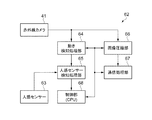
すなわち、本実施形態では、図8(a)に示したように電子機器としてのセンサーデバイス35は、センサーアレイ36と、行選択回路37と、読み出し回路38を含む。さらに、センサーデバイス35はA/D変換部39、制御回路40を含む。行選択回路37を行ドライバーとも称す。第1の実施形態における駆動回路9は行選択回路37、読み出し回路38、A/D変換部39、制御回路40等を備えている。センサーデバイス35を用いることで例えばナイトビジョン機器等に用いられる赤外線カメラ等を実現できる。
That is, in the present embodiment, as shown in FIG. 8A, the
図8(a)に示すように、センサーデバイス35はセンサーアレイ36を備えている。図8(b)に示すように、センサーアレイ36には複数の赤外線検出素子3が格子状に配列される。複数の行線と複数の列線との配線が設けられている。行線はワード線や走査線とも称し、列線はデータ線とも称す。尚、行線及び列線の一方の本数は1本であってもよい。例えば行線が1本である場合には行線に沿った方向(図中横方向)に複数の赤外線検出素子3が配列される。一方、列線が1本である場合には列線に沿った方向(図中縦方向)に複数の赤外線検出素子3が配列される。
As shown in FIG. 8A, the
センサーアレイ36の各赤外線検出素子3は、各行線と各列線の交差位置に対応する場所に配置される。例えば、行線WL1と列線DL1の交差位置に対応する場所に赤外線検出素子3の1つが配置されている。他の赤外線検出素子3も同様に配置されている。センサーアレイ36のサイズは特に限定されない。本実施形態では例えばセンサーアレイ36は320×240画素のQVGA(Quarter Video Graphics Array)となっている。そして、行線WL0、WL1、WL2・・・・WL239及び列線DL0、DL1、DL2・・・・DL319が配置されている。
Each
図8(a)に戻って、行選択回路37は複数の行線に接続される。そして各行線の選択動作を行う。つまり、行線WL0、WL1、WL2・・・・WL239を順次選択して走査する動作を行う。即ちこれらの行線を選択する信号であるワード選択信号をセンサーアレイ36に出力する。
Returning to FIG. 8A, the
読み出し回路38は、複数の列線に接続され、各列線の読み出し動作を行う。QVGAのセンサーアレイ36を例にとれば、列線DL0、DL1、DL2・・・・DL319からの検出信号(検出電流、検出電荷)を読み出す動作を行う。
The
A/D変換部39は、読み出し回路38において取得された検出電圧(測定電圧、到達電圧)をデジタルデータにA/D変換する処理を行う。そしてA/D変換後のデジタルデータDOUTを出力する。具体的には、A/D変換部39には、複数の列線の各列線に対応して各A/D変換器が設けられる。そして、各A/D変換器は、対応する列線において読み出し回路38により取得された検出電圧のA/D変換処理を行う。尚、複数の列線に対応して1つのA/D変換器を設け、この1つのA/D変換器を用いて、複数の列線の検出電圧を時分割にA/D変換してもよい。
The A /
制御回路40は、各種の制御信号を生成して、行選択回路37、読み出し回路38、A/D変換部39に出力する。例えば、充電や放電(リセット)の制御信号を生成して出力する。或いは、各回路のタイミングを制御する信号を生成して出力する。第1の実施形態における駆動回路9は行選択回路37、読み出し回路38、A/D変換部39及び制御回路40等により構成されている。
The
上述したように、本実施形態によれば、以下の効果を有する。
(1)本実施形態によれば、センサーデバイス35は格子状に配列した赤外線検出素子3を備えている。そして、行選択回路37及び読み出し回路38が順次赤外線検出素子3を選択して赤外線の受光量を検出して出力する。赤外線検出素子3は支持部23が凹部15に張り付かずに感度良く赤外線の受光量を検出する。従って、センサーデバイス35は照射される赤外線の分布を感度良く検出する赤外線検出素子3を備えた装置とすることができる。
As described above, this embodiment has the following effects.
(1) According to the present embodiment, the
(第3の実施形態)
次に、赤外線検出部に赤外線検出素子を備える電子機器の1つである赤外線カメラの一実施形態について図9の赤外線カメラの構成を示すブロック図を用いて説明する。図9に示すように、電子機器としての赤外線カメラ41は、光学系42、光検出部43、画像処理部44、処理部45、記憶部46、操作部47、表示部48を含んで構成されている。
(Third embodiment)
Next, an embodiment of an infrared camera that is one of electronic devices including an infrared detection element in the infrared detection unit will be described with reference to a block diagram showing the configuration of the infrared camera in FIG. As shown in FIG. 9, the
光学系42は、例えば1枚または複数枚のレンズやレンズの位置を移動させる駆動部等を含んで構成されている。そして、光学系42は光検出部43への物体像の結像を行う。必要に応じて光学系42はフォーカス調整や絞り調整等の機能も備えても良い。
The
光検出部43には上記実施形態の赤外線検出素子3が二次元配列された検出器が用いられている。光検出部43は、検出器に加えて行選択回路(行ドライバー)、列線を介して検出器からのデータを読み出す読み出し回路及びA/D変換部等を備えている。そして、二次元配列された各検出器からのデータを順次読み出すことで、被写体の画像データを形成することができる。
The
画像処理部44は、光検出部43からのデジタルの画像データに基づいて、画像補正処理等の各種の画像処理を行う。画像データは画素データとも称す。
The
処理部45は、赤外線カメラ41の全体の制御を行い、赤外線カメラ41内の各ブロックの制御を行う。この処理部45は例えばCPU等により実現される。記憶部46は各種の情報を記憶するものであり、例えば処理部45や画像処理部44のワーク領域として機能する。操作部47は、操作者が赤外線カメラ41を操作するためのインターフェイスとなるものであり、例えば、各種ボタンやGUI(Graphical User Interface)画面等により実現される。表示部48は、例えば光検出部43により取得された画像やGUI画面等を表示するものであり、液晶ディスプレイや有機ELディスプレイ等の各種のディスプレイにより実現される。
The
このように、直交する二方向に赤外線検出素子3を二次元配置された光検出部43を用いて熱(光)分布画像を提供することができる。この光検出部43を用いて、サーモグラフィー、車載用ナイトビジョンあるいは監視カメラ等の電子機器を構成することができる。
In this way, a heat (light) distribution image can be provided using the
もちろん、1セル分または複数セルの赤外線検出素子3をセンサーとして用いることで物体の物理情報の解析(測定)を行う解析機器(測定機器)、火や発熱を検知するセキュリティー機器、工場等に設けられるFA(Factory Automation)機器等の各種の電子機器を構成することもできる。
Of course, it is installed in analysis equipment (measuring equipment) that analyzes (measures) physical information of objects by using the infrared detecting
上述したように、本実施形態によれば、以下の効果を有する。
(1)本実施形態によれば、赤外線カメラ41は光検出部43を備え、光検出部43には赤外線検出素子3が用いられている。赤外線検出素子3は支持部23が凹部15に張り付かずに感度良く赤外線の受光量を検出する。光検出部43の赤外線検出素子3は感度良く赤外線を検出するので、赤外線カメラ41は感度良く赤外線を検出する赤外線検出素子を備えた電子機器とすることができる。
As described above, this embodiment has the following effects.
(1) According to this embodiment, the
(第4の実施形態)
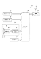
次に、光検出部に赤外線検出素子を備えた赤外線カメラを用いた電子機器の1つである運転支援装置の一実施形態について図10及び図11を用いて説明する。図10は、運転支援装置の構成を示すブロック図であり、図11は、運転支援装置を搭載した自動車を示す概略斜視図である。
(Fourth embodiment)
Next, an embodiment of a driving support device that is one of electronic devices using an infrared camera provided with an infrared detection element in a light detection unit will be described with reference to FIGS. 10 and 11. FIG. 10 is a block diagram showing the configuration of the driving support device, and FIG. 11 is a schematic perspective view showing an automobile equipped with the driving support device.
図10に示すように、電子機器としての運転支援装置51は、運転支援装置51を制御するCPUを備えた処理ユニット52と、車両外部の所定の撮像領域における赤外線を検出可能な赤外線カメラ41と、車両のヨーレートを検出するヨーレートセンサー54とを備えている。さらに、運転支援装置51は、車両の走行速度を検出する車速センサー55と、運転者のブレーキ操作の有無を検出するブレーキセンサー56と、スピーカー57と、表示装置58とを備えて構成されている。そして、本実施形態の赤外線カメラ41は上記実施形態における赤外線カメラ41と同じカメラが用いられている。従って、赤外線カメラ41は光検出部に赤外線検出素子3を備えている。
As shown in FIG. 10, a driving
この運転支援装置51の処理ユニット52は、例えば、赤外線カメラ41の撮像により得られる自車両周辺の赤外線画像と、ヨーレートセンサー54、車速センサー55、ブレーキセンサー56により検出される自車両の走行状態にかかる検出信号を用いる。そして、処理ユニット52は赤外線画像及び検出信号を用いて自車両の進行方向前方に存在する物体及び歩行者等の対象物を検出する。検出した対象物と自車両との接触が発生する可能性があると判断したときには、スピーカー57または表示装置58により警報を出力する。
For example, the
図11に示すように、赤外線カメラ41は、自動車の前部において車幅方向の中心付近に配置されている。表示装置58は、フロントウィンドーにおいて運転者の前方視界を妨げない位置に各種情報を表示するHUD(Head Up Display)59等を備えて構成されている。
As shown in FIG. 11, the
(1)本実施形態によれば、運転支援装置51は赤外線カメラ41を備えている。赤外線カメラ41は光検出部43を備え、光検出部43には上記実施形態の赤外線検出素子3が用いられている。赤外線検出素子3は支持部23が凹部15に張り付かずに感度良く赤外線の受光量を検出する。従って、運転支援装置51は感度良く赤外線を検出する赤外線検出素子を有する赤外線カメラ41を備えた電子機器とすることができる。
(1) According to the present embodiment, the driving
(第5の実施形態)
次に、赤外線検出部に赤外線検出素子を備えた赤外線カメラを用いた電子機器の1つであるセキュリティー機器の一実施形態について図12及び図13を用いて説明する。図12は、セキュリティー機器の構成を示すブロック図であり、図13はセキュリティー機器が設置された家を示す模式図である。
(Fifth embodiment)
Next, an embodiment of a security device that is one of electronic devices using an infrared camera provided with an infrared detection element in an infrared detection unit will be described with reference to FIGS. FIG. 12 is a block diagram illustrating a configuration of the security device, and FIG. 13 is a schematic diagram illustrating a house in which the security device is installed.
図12に示すように、電子機器としてのセキュリティー機器62は、監視エリアを撮影する赤外線カメラ41と、監視エリアへの侵入者を検知する人感センサー63を備える。人感センサー63は光検出部を備え、光検出部に赤外線検出素子3を備えている。そして、本実施形態の赤外線カメラ41は上記実施形態における赤外線カメラ41と同じカメラが用いられている。従って、赤外線カメラ41は光検出部に赤外線検出素子3を備えている。
As shown in FIG. 12, a
さらに、セキュリティー機器62は、赤外線カメラ41から出力された画像データを処理して監視エリアに侵入した移動体を検知する動き検知処理部64を備える。さらに、セキュリティー機器62は人感センサー63が出力する信号を用いて侵入者の検知処理を行う人感センサー検知処理部65を備える。さらに、セキュリティー機器62は画像圧縮部66を備え、画像圧縮部66は赤外線カメラ41から出力された画像データを所定の方式で圧縮する。さらに、セキュリティー機器62は通信処理部67を備え、通信処理部67は圧縮された画像データや侵入者検知情報を外部装置に送信し、セキュリティー機器62への各種設定情報等を外部装置から受信する。さらに、セキュリティー機器62は制御部68等を備え、制御部68はセキュリティー機器62の各処理部に対して条件設定、処理コマンド送信、レスポンス処理をCPU(Central Processing Unit)にて行う。セキュリティー機器62は以上の要素等で構成されている。そして、本実施形態の赤外線カメラ41は上記実施形態における赤外線カメラ41と同じカメラが用いられている。従って、赤外線カメラ41は光検出部に赤外線検出素子3を備えている。
Furthermore, the
動き検知処理部64は、図示しないバッファメモリーと、バッファメモリーの出力信号が入力されるブロックデータ平滑部と、ブロックデータ平滑部の出力信号が入力される状態変化検出部とを備える。そして、状態変化検出部は撮影した動画の画像であるフレームを比較する。そして、監視エリアが静止状態であれば動画で撮影した異なるフレームが同一画像の画像データとなり、移動体の侵入による状態変化があるときフレーム間の画像データで差が生じる。フレーム間の画像データで差を利用して状態変化検出部は状態変化を検知する。
The motion
図13に示すように、セキュリティー機器62は軒下に赤外線カメラ41及び人感センサー63が設置されている。そして、赤外線カメラ41は撮像エリア69を検出し、人感センサー63は検知エリア70を検出する。
As shown in FIG. 13, the
(1)本実施形態によれば、セキュリティー機器62は人感センサー63及び赤外線カメラ41を備えている。人感センサー63及び赤外線カメラ41は光検出部を備え、光検出部には赤外線検出素子3が用いられている。赤外線検出素子3は支持部23が凹部15に張り付かずに感度良く赤外線の受光量を検出する。従って、セキュリティー機器62は感度良く赤外線を検出する赤外線検出素子を有する人感センサー63及び赤外線カメラ41を備えた電子機器とすることができる。
(1) According to the present embodiment, the
(第6の実施形態)
次に、赤外線検出部に赤外線検出素子を備えた赤外線カメラを用いた電子機器の1つであるゲーム機器の一実施形態について図14及び図15を用いて説明する。図14は、ゲーム機器のコントローラーの構成を示すブロック図であり、図15はコントローラーの使用方法を説明するための模式図である。
(Sixth embodiment)
Next, an embodiment of a game device that is one of electronic devices using an infrared camera provided with an infrared detection element in an infrared detection unit will be described with reference to FIGS. FIG. 14 is a block diagram showing the configuration of the controller of the game device, and FIG. 15 is a schematic diagram for explaining how to use the controller.
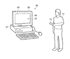
図14に示すように、ゲーム機器に用いられる電子機器としてのコントローラー73は、撮像情報演算ユニット74と、操作スイッチ75と、加速度センサー76と、コネクター77と、プロセッサー78と、無線モジュール79と、を備えて構成される。
As shown in FIG. 14, a
撮像情報演算ユニット74は、撮像ユニット80と、この撮像ユニット80で撮像した画像データを処理するための画像処理回路81とを有する。撮像ユニット80は光検出部82を備え、さらに、光検出部82と接続して赤外線だけを通すフィルターである赤外線フィルター83及びレンズ等の光学系84を備えている。そして、画像処理回路81は、撮像ユニット80から得られた赤外線画像データを処理して、高輝度部分を検知し、高輝度部分の重心位置や面積を検出してこれらのデータを出力する。光検出部82には上記実施形態の赤外線検出素子3が用いられている。
The imaging
プロセッサー78は、操作スイッチ75からの操作データと、加速度センサー76からの加速度データ及び赤外線画像の高輝度部分データを一連のコントロールデータとして無線モジュール79に出力する。無線モジュール79は所定周波数の搬送波をこのコントロールデータで変調する。無線モジュール79はアンテナ85を備え、アンテナ85から搬送波を電波信号にして出力する。
The
尚、コントローラー73に設けられているコネクター77を通して入力されたデータもプロセッサー78によって上述のデータと同様に処理されてコントロールデータとして無線モジュール79とアンテナ85を介して出力される。
Data input through the
図15に示すように、電子機器としてのゲーム機器86は、コントローラー73と、ゲーム機本体87と、ディスプレイ88と、LEDモジュール89及びLEDモジュール90とを備えている。ゲーム機器86を操作するプレイヤー91は一方の手でコントローラー73を操作してゲームをプレイすることができる。そして、コントローラー73の撮像ユニット80をディスプレイ88の画面92を向くようにすると、ディスプレイ88の近傍に設置された二つのLEDモジュール89及びLEDモジュール90から出力される赤外線を撮像ユニット80が検知する。そして、コントローラー73は、二つのLEDモジュール89,90の位置や面積情報を高輝度点の情報として取得する。輝点の位置や大きさのデータがコントローラー73から無線でゲーム機本体87に送信され、ゲーム機本体87に受信される。プレイヤー91がコントローラー73を動かすと、輝点の位置や大きさのデータが変化する。それを利用して、ゲーム機本体87はコントローラー73の動きに対応した操作信号を取得できる。そして、操作信号にしたがってゲーム機器86はゲームを進行させることができる。
As shown in FIG. 15, the
上述したように、本実施形態によれば、以下の効果を有する。
(1)本実施形態によれば、ゲーム機器86のコントローラー73は光検出部82を備え、光検出部82には上記実施形態の赤外線検出素子3が用いられている。赤外線検出素子3は支持部23が凹部15に張り付かずに感度良く赤外線の受光量を検出する。光検出部82の赤外線検出素子3は感度良く赤外線を検出するので、ゲーム機器86は感度良く赤外線を検出する赤外線検出素子3が設置されたコントローラー73を有する電子機器とすることができる。
As described above, this embodiment has the following effects.
(1) According to this embodiment, the
(第7の実施形態)
次に、赤外線検出部に赤外線検出素子を備えた赤外線カメラを用いた電子機器の1つである体温測定装置の一実施形態について図16を用いて説明する。図16は、体温測定装置の構成を示すブロック図である。
(Seventh embodiment)
Next, an embodiment of a body temperature measuring device which is one of electronic devices using an infrared camera provided with an infrared detection element in an infrared detection unit will be described with reference to FIG. FIG. 16 is a block diagram showing a configuration of the body temperature measuring device.
図16に示すように、電子機器としての体温測定装置95は、赤外線カメラ41と、体温分析装置96と、情報通信装置97と、ケーブル98とを備えて構成されている。本実施形態の赤外線カメラ41は上記の実施形態の赤外線カメラ41と同じカメラが用いられている。
As shown in FIG. 16, a body
赤外線カメラ41は所定の対象領域を撮影し、撮影された対象者99の画像情報をケーブル98を経由して体温分析装置96に送信する。体温分析装置96は、赤外線カメラ41からの熱分布画像を読み取る画像読取処理ユニットと、画像読取処理ユニットからのデータと画像分析設定テーブルに基づいて体温分析テーブルを作成する体温分析処理ユニットとを含み、体温分析テーブルに基づいて体温情報送信用データを情報通信装置97へ送信する。この体温情報送信用データは体温異常であることに対応する所定のデータを含んでもよい。また、撮影領域内に複数の対象者99を含んでいると判断した場合には、対象者99の人数と体温異常者の人数の情報を体温情報送信用データに含んでもよい。
The
上述したように、本実施形態によれば、以下の効果を有する。
(1)本実施形態によれば、体温測定装置95は赤外線カメラ41を備えている。赤外線カメラ41は光検出部を備え、光検出部には赤外線検出素子3が用いられている。赤外線検出素子3は支持部23が凹部15に張り付かずに感度良く赤外線の受光量を検出する。従って、体温測定装置95は感度良く赤外線を検出する赤外線検出素子を有する赤外線カメラ41を備えた電子機器とすることができる。
As described above, this embodiment has the following effects.
(1) According to this embodiment, the body
(第8の実施形態)
次に、光検出部に赤外線検出素子を備える電子機器の1つである特定物質探知装置の一実施形態について図17の特定物質探知装置の構成を示すブロック図を用いて説明する。
(Eighth embodiment)
Next, an embodiment of a specific substance detection device that is one of electronic devices including an infrared detection element in the light detection unit will be described with reference to a block diagram showing the configuration of the specific substance detection device in FIG.
図17に示すように電子機器としての特定物質探知装置102は、制御ユニット103と、照射光ユニット104と、光学フィルター105と、撮像ユニット106と、表示部107とを備えて構成されている。撮像ユニット106は、図示しないレンズ等の光学系と光検出部を備え、該光検出部は第1の実施形態の赤外線検出素子3を備えている。そして、赤外線検出素子3の赤外線検出部4が備える赤外線吸収膜30の吸収波長はテラヘルツ域となっている。
As shown in FIG. 17, the specific
制御ユニット103は、本装置全体を制御するシステムコントローラーを含み、該システムコントローラーは制御ユニットに含まれる光源駆動部及び画像処理ユニットを制御する。照射光ユニット104は、波長が100μm〜1000μmの範囲にある電磁波であるテラヘルツ光を射出するレーザー装置と光学系を含み、テラヘルツ光を検査対象の人物108に照射する。
The
人物108と撮像ユニット106との間には光学フィルター105が配置されている。光学フィルター105は探知対象である特定物質109の分光スペクトルのみを通過させる。人物108から反射するテラヘルツ光は、光学フィルター105にて分離されて特定物質109の分光スペクトルのみ撮像ユニット106に受光される。撮像ユニット106で生成された画像信号は、制御ユニット103の画像処理ユニットで所定の画像処理が施され、その画像信号が表示部107へ出力される。そして人物108の衣服内等に特定物質109が存在するか否かにより受光信号の強度が異なるので特定物質109の存在が判別できる。
An
上述したように、本実施形態によれば、以下の効果を有する。
(1)本実施形態によれば、特定物質探知装置102は撮像ユニット106に光検出部を備え、光検出部には上記実施形態の赤外線検出素子3が用いられている。赤外線検出素子3は支持部23が凹部15に張り付かずに感度良く赤外線の受光量を検出する。光検出部の赤外線検出素子3は感度良く赤外線を検出するので、特定物質探知装置102は撮像ユニット106に感度良く赤外線を検出する赤外線検出素子を備えた電子機器とすることができる。
As described above, this embodiment has the following effects.
(1) According to this embodiment, the specific
以上、いくつかの実施形態について説明したが、本発明の新規事項及び効果から実体的に逸脱しない多くの変形が可能であることは当業者には容易に理解できるものである。従って、このような変形例は総て本発明の範囲に含まれるものとする。例えば、明細書または図面において、少なくとも一度、より広義または同義な異なる用語と共に記載された用語は、明細書または図面のいかなる箇所においても、その異なる用語に置き換えることができる。 Although several embodiments have been described above, those skilled in the art can easily understand that many modifications are possible without departing from the novel matters and effects of the present invention. Accordingly, all such modifications are included in the scope of the present invention. For example, a term described at least once together with a different term having a broader meaning or the same meaning in the specification or the drawings can be replaced with the different term anywhere in the specification or the drawings.
本発明は、種々の焦電型検出器に広く適用することができる。検出する光の波長は問わない。また、焦電型検出器または焦電型検出装置、あるいはそれらを有する電子機器は、例えば、供給する熱量と流体が奪う熱量とが均衡する条件下にて流体の流量を検出するフローセンサー等にも適用できる。このフローセンサーに設けられる熱電対等に代えて本発明の焦電型検出器または焦電型検出装置を設けることができ、光以外を検出対象とすることができる。 The present invention can be widely applied to various pyroelectric detectors. The wavelength of the light to detect is not ask | required. In addition, the pyroelectric detector or the pyroelectric detection device, or the electronic apparatus having them, can be used as, for example, a flow sensor that detects the flow rate of a fluid under a condition where the amount of heat supplied and the amount of heat taken by the fluid are balanced. Is also applicable. Instead of the thermocouple or the like provided in the flow sensor, the pyroelectric detector or pyroelectric detection device of the present invention can be provided, and objects other than light can be detected.
尚、本実施形態は上述した実施形態に限定されるものではなく、種々の変更や改良を加えることも可能である。変形例を以下に述べる。 In addition, this embodiment is not limited to embodiment mentioned above, A various change and improvement can also be added. A modification will be described below.
(変形例1)
前記第1の実施形態では、2つの梁22が設置されたが、梁22の個数は限定されない。梁22の個数は1個でも良く、3個以上でも良い。支持部23を安定して支持できれば良い。また、梁22は折れ曲がった角柱状であったが、梁22の形状は曲線でも良く、真直ぐでもよい。支持部23を安定して支持できれば良く、設計し易い形状にしても良い。また、梁22を長くすることにより梁22を介して熱伝導する熱量を減らすことができる。
(Modification 1)
In the first embodiment, two
(変形例2)
前記第1の実施形態では、基板2上に駆動回路9を設置し、同じ基板2上に赤外線検出素子3を配列して形成した。駆動回路9は基板2でなく外部基板に設置しても良い。バンプを接点に用いて基板2と外部基板との間で通信しても良い。良品の駆動回路9と赤外線検出素子3が配列した良品のセンサーアレイとを組み立ててセンサーデバイスとする。従って、歩留まり良くセンサーデバイスを製造できるので、生産性良くセンサーデバイスを製造することできる。
(Modification 2)
In the first embodiment, the
(変形例3)
前記第1の実施形態では、ステップS12の検出部形成工程の後にステップS9の支持部形成工程を行った。ステップS9はステップS5の支持部材形成工程とステップS6の貫通電極形成工程との間に行われても良い。また、ステップS9はステップS6の貫通電極形成工程とステップS12の検出部形成工程との間に行われても良い。製造し易いステップ順にて行っても良い。
(Modification 3)
In the first embodiment, the support portion forming step of Step S9 is performed after the detection portion forming step of Step S12. Step S9 may be performed between the support member forming process of step S5 and the through electrode forming process of step S6. Further, step S9 may be performed between the through electrode forming process of step S6 and the detecting portion forming process of step S12. You may carry out in order of the step which is easy to manufacture.
(変形例4)
前記第1の実施形態では、支持部材20をSiNの膜にした。支持部材20の空隙17側にはポリシリコンの膜を配置しても良い。これにより、空隙17と接する場所を純水に対して撥水性を良くすることができる。従って、空隙17から純水を排出しやすくなるので、支持部23が凹部15の底に吸着することをさらに防止することができる。
(Modification 4)
In the first embodiment, the
(変形例5)
前記第1の実施形態では、ステップS3の撥水膜形成工程にて撥水膜16を成膜した。続けて撥水膜16をパターニングした。撥水膜16のパターニングはステップS4の犠牲膜形成工程にてCMP法を用いて犠牲膜32の上面を平坦にする工程にて行っても良い。撥水膜16のパターニングは凹部15以外の場所の撥水膜16を除去する内容であり、犠牲膜32の上面を平坦にすることによりパターニングすることができる。この方法を用いることにより、マスクを形成する工程とドライエッチングする工程とを削減することができる。その結果、生産性良く赤外線検出素子3を製造することができる。
(Modification 5)
In the first embodiment, the
(変形例6)
前記第1の実施形態では、ステップS9の支持部形成工程の後にステップS10の赤外線吸収膜形成工程を行った。ステップS10の後にステップS9を行っても良い。つまり、赤外線検出部4に赤外線吸収膜30を成膜した後で梁22及び支持部23の形状をパターニングしても良い。製造し易い工程順にて製造しても良い。
(Modification 6)
In the said 1st Embodiment, the infrared rays absorption film formation process of step S10 was performed after the support part formation process of step S9. Step S9 may be performed after step S10. That is, the shape of the
(変形例7)
前記第1の実施形態では、ステップS11のエッチング工程において純水を用いて洗浄し乾燥した。純水にて洗浄した後にアルコール等の沸点の低い液体で水置換しても良い。さらに、凹部15から液体が早く排出されるので支持部23を凹部15の底に張り付き難くすることができる。
(Modification 7)
In the first embodiment, cleaning is performed using pure water and drying is performed in the etching process of step S11. After washing with pure water, water may be substituted with a liquid having a low boiling point such as alcohol. Further, since the liquid is quickly discharged from the
(変形例8)
前記第1の実施形態では、ステップS11のエッチング工程において、基板2をフッ化水素のエッチング液に浸漬した。尚、エッチング液はフッ化水素酸とフッ化アンモニウムとを混合したバッファードフッ酸を用いても良い。
(Modification 8)
In the first embodiment, in the etching process of step S11, the
2…基板、4…赤外線検出部、14…絶縁膜、15…凹部、16…撥水膜、17…空隙、22…梁、23…支持部、24…下部電極、25…焦電体、26…上部電極、32…犠牲膜、35…電子機器としてのセンサーデバイス、41…電子機器としての赤外線カメラ、43,82…光検出部、51…電子機器としての運転支援装置、62…電子機器としてのセキュリティー機器、73…電子機器としてのコントローラー、86…電子機器としてのゲーム機器、95…電子機器としての体温測定装置、102…電子機器としての特定物質探知装置。
DESCRIPTION OF
Claims (5)
前記基板上に設置され凹部を備えた絶縁膜と、
前記基板に一端が固定される梁によって保持され前記凹部の上方に空隙を介して位置する支持部と、
前記支持部上に設置され赤外線を検出する赤外線検出部と、を備え、
前記凹部はポリシリコンを含む撥水膜に覆われ、前記梁及び前記支持部は窒化シリコンまたは炭窒化シリコンを含むことを特徴とする赤外線検出素子。 A substrate,
An insulating film installed on the substrate and provided with a recess;
A support part which is held by a beam whose one end is fixed to the substrate and is located above the concave part via a gap;
An infrared detection unit installed on the support unit for detecting infrared rays,
The infrared detecting element, wherein the recess is covered with a water-repellent film containing polysilicon, and the beam and the support part contain silicon nitride or silicon carbonitride.
前記赤外線検出部は前記支持部上に下部電極、焦電体、上部電極が重ねて配置され、
前記支持部は窒化シリコンを含み、前記焦電体は優先配向していることを特徴とする赤外線検出素子。 The infrared detection element according to claim 1,
The infrared detection unit is arranged such that a lower electrode, a pyroelectric body, and an upper electrode are stacked on the support unit,
The infrared detecting element, wherein the support portion includes silicon nitride, and the pyroelectric material is preferentially oriented.
前記絶縁膜に凹部を形成する凹部形成工程と、
前記凹部を覆って撥水膜を形成する撥水膜形成工程と、
前記凹部に犠牲膜を形成する犠牲膜形成工程と、
前記犠牲膜上に支持部材を成膜する支持部材形成工程と、
前記支持部材上に赤外線検出部を形成する検出部形成工程と、
前記支持部材を、前記赤外線検出部を支持する支持部及び前記支持部を保持する梁の形状にパターニングする支持部形成工程と、
前記犠牲膜をエッチングするエッチング工程と、を有し、
前記撥水膜はポリシリコンを含み、前記支持部材は窒化シリコンまたは炭窒化シリコンを含むことを特徴とする赤外線検出素子の製造方法。 An insulating film forming step of forming an insulating film on the substrate;
A recess forming step of forming a recess in the insulating film;
A water repellent film forming step of covering the recess and forming a water repellent film;
A sacrificial film forming step of forming a sacrificial film in the recess;
A support member forming step of forming a support member on the sacrificial film;
A detection unit forming step of forming an infrared detection unit on the support member;
A support part forming step of patterning the support member into a shape of a support part that supports the infrared detection part and a beam that holds the support part;
An etching step of etching the sacrificial film,
The method of manufacturing an infrared detecting element, wherein the water repellent film includes polysilicon, and the support member includes silicon nitride or silicon carbonitride.
前記犠牲膜形成工程において前記撥水膜の一部を露出させ、
前記支持部材形成工程において露出された前記撥水膜の表面をエッチングして、前記撥水膜上に前記支持部材を重ねて配置することを特徴とする赤外線検出素子の製造方法。 It is a manufacturing method of the infrared detection element according to claim 3,
Exposing part of the water-repellent film in the sacrificial film forming step;
Etching the surface of the water-repellent film exposed in the support member forming step, and placing the support member on the water-repellent film, the method for manufacturing an infrared detecting element.
前記光検出部に請求項1または2に記載の赤外線検出素子を備えることを特徴とする電子機器。 An electronic device including a light detection unit that detects infrared rays,
An electronic apparatus comprising the infrared detection element according to claim 1 or 2 in the light detection unit.
Priority Applications (4)
| Application Number | Priority Date | Filing Date | Title |
|---|---|---|---|
| JP2011194658A JP2013057526A (en) | 2011-09-07 | 2011-09-07 | Infrared sensor, manufacturing method therefor, and electronic apparatus |
| US13/601,274 US8957375B2 (en) | 2011-09-07 | 2012-08-31 | Infrared detecting element, method for manufacturing infrared detecting element, and electronic device |
| CN2012103243665A CN102998003A (en) | 2011-09-07 | 2012-09-04 | Infrared detecting element, method for manufacturing infrared detecting element, and electronic device |
| US14/604,076 US9255845B2 (en) | 2011-09-07 | 2015-01-23 | Infrared detecting element, method for manufacturing infrared detecting element, and electronic device |
Applications Claiming Priority (1)
| Application Number | Priority Date | Filing Date | Title |
|---|---|---|---|
| JP2011194658A JP2013057526A (en) | 2011-09-07 | 2011-09-07 | Infrared sensor, manufacturing method therefor, and electronic apparatus |
Publications (2)
| Publication Number | Publication Date |
|---|---|
| JP2013057526A true JP2013057526A (en) | 2013-03-28 |
| JP2013057526A5 JP2013057526A5 (en) | 2014-10-16 |
Family
ID=47752381
Family Applications (1)
| Application Number | Title | Priority Date | Filing Date |
|---|---|---|---|
| JP2011194658A Withdrawn JP2013057526A (en) | 2011-09-07 | 2011-09-07 | Infrared sensor, manufacturing method therefor, and electronic apparatus |
Country Status (3)
| Country | Link |
|---|---|
| US (2) | US8957375B2 (en) |
| JP (1) | JP2013057526A (en) |
| CN (1) | CN102998003A (en) |
Cited By (1)
| Publication number | Priority date | Publication date | Assignee | Title |
|---|---|---|---|---|
| JP2020077779A (en) * | 2018-11-08 | 2020-05-21 | 富士通株式会社 | Photo detection element, photosensor and method of manufacturing photo detection element |
Families Citing this family (6)
| Publication number | Priority date | Publication date | Assignee | Title |
|---|---|---|---|---|
| US20140198195A1 (en) * | 2013-01-17 | 2014-07-17 | Electronics And Telecommunications Research Institute | Terahertz health checker |
| US10057508B2 (en) * | 2013-06-20 | 2018-08-21 | Excelitas Technologies Corp. | Illumination device with integrated thermal imaging sensor |
| CN105258806A (en) * | 2015-11-02 | 2016-01-20 | 电子科技大学 | Pyroelectric infrared detection unit and manufacture method thereof, and pyroelectric infrared detector |
| KR20180069147A (en) * | 2016-12-14 | 2018-06-25 | 만도헬라일렉트로닉스(주) | Apparatus for warning pedestrian in vehicle |
| US10984640B2 (en) * | 2017-04-20 | 2021-04-20 | Amazon Technologies, Inc. | Automatic adjusting of day-night sensitivity for motion detection in audio/video recording and communication devices |
| US10199424B1 (en) * | 2017-07-19 | 2019-02-05 | Meridian Innovation Pte Ltd | Thermoelectric-based infrared detector having a cavity and a MEMS structure defined by BEOL metals lines |
Citations (4)
| Publication number | Priority date | Publication date | Assignee | Title |
|---|---|---|---|---|
| JP2002361596A (en) * | 2001-03-29 | 2002-12-18 | Toyota Central Res & Dev Lab Inc | Manufacturing method and device for silicon series structure |
| JP2006099073A (en) * | 2004-09-27 | 2006-04-13 | Idc Llc | System and method of providing mems device with anti-stiction coating |
| JP2010127657A (en) * | 2008-11-25 | 2010-06-10 | Panasonic Electric Works Co Ltd | Infrared sensor and method for manufacturing the same |
| JP2011153853A (en) * | 2010-01-26 | 2011-08-11 | Seiko Epson Corp | Thermal photodetector, thermal photodetector device, electronic instrument, and method of manufacturing thermal photodetector |
Family Cites Families (15)
| Publication number | Priority date | Publication date | Assignee | Title |
|---|---|---|---|---|
| US6590710B2 (en) | 2000-02-18 | 2003-07-08 | Yokogawa Electric Corporation | Fabry-Perot filter, wavelength-selective infrared detector and infrared gas analyzer using the filter and detector |
| JP2002174721A (en) | 2000-12-06 | 2002-06-21 | Yokogawa Electric Corp | Fabry-perot filter |
| JP3409848B2 (en) * | 2000-08-29 | 2003-05-26 | 日本電気株式会社 | Thermal infrared detector |
| US20040094086A1 (en) | 2001-03-29 | 2004-05-20 | Keiichi Shimaoka | Production device and production method for silicon-based structure |
| WO2002101836A1 (en) * | 2001-06-12 | 2002-12-19 | Hitachi, Ltd. | Semiconductor device and method of producing the same |
| FR2826725B1 (en) * | 2001-06-28 | 2004-02-27 | Commissariat Energie Atomique | MICROBOLOMETERS RESISTANT TO TEMPERATURES OF HIGH SCENES. |
| JP3862080B2 (en) * | 2002-11-01 | 2006-12-27 | 防衛庁技術研究本部長 | Method for manufacturing thermal infrared detector |
| CN1755433A (en) * | 2004-09-27 | 2006-04-05 | Idc公司 | System and method of providing mems device with anti-stiction coating |
| JP5109169B2 (en) | 2007-03-27 | 2012-12-26 | 日本電気株式会社 | Bolometer type THz wave detector |
| JP4978501B2 (en) | 2008-02-14 | 2012-07-18 | 日本電気株式会社 | Thermal infrared detector and method for manufacturing the same |
| JP2011027780A (en) | 2009-07-21 | 2011-02-10 | Denso Corp | Fabry-perot interferometer and manufacturing method of the same |
| JP5750827B2 (en) * | 2010-01-26 | 2015-07-22 | セイコーエプソン株式会社 | Method for manufacturing thermal detector |
| JP5771900B2 (en) | 2010-03-26 | 2015-09-02 | セイコーエプソン株式会社 | Thermal photodetector, thermal photodetector, and electronic device |
| JP5964543B2 (en) * | 2010-06-15 | 2016-08-03 | 日本電気株式会社 | Bolometer type terahertz wave detector |
| CN102564601A (en) * | 2010-12-22 | 2012-07-11 | 精工爱普生株式会社 | Thermal detector, thermal detection device, electronic instrument, and thermal detector manufacturing method |
-
2011
- 2011-09-07 JP JP2011194658A patent/JP2013057526A/en not_active Withdrawn
-
2012
- 2012-08-31 US US13/601,274 patent/US8957375B2/en active Active
- 2012-09-04 CN CN2012103243665A patent/CN102998003A/en active Pending
-
2015
- 2015-01-23 US US14/604,076 patent/US9255845B2/en not_active Expired - Fee Related
Patent Citations (4)
| Publication number | Priority date | Publication date | Assignee | Title |
|---|---|---|---|---|
| JP2002361596A (en) * | 2001-03-29 | 2002-12-18 | Toyota Central Res & Dev Lab Inc | Manufacturing method and device for silicon series structure |
| JP2006099073A (en) * | 2004-09-27 | 2006-04-13 | Idc Llc | System and method of providing mems device with anti-stiction coating |
| JP2010127657A (en) * | 2008-11-25 | 2010-06-10 | Panasonic Electric Works Co Ltd | Infrared sensor and method for manufacturing the same |
| JP2011153853A (en) * | 2010-01-26 | 2011-08-11 | Seiko Epson Corp | Thermal photodetector, thermal photodetector device, electronic instrument, and method of manufacturing thermal photodetector |
Cited By (2)
| Publication number | Priority date | Publication date | Assignee | Title |
|---|---|---|---|---|
| JP2020077779A (en) * | 2018-11-08 | 2020-05-21 | 富士通株式会社 | Photo detection element, photosensor and method of manufacturing photo detection element |
| JP7260736B2 (en) | 2018-11-08 | 2023-04-19 | 富士通株式会社 | Photodetector, optical sensor, and method for manufacturing photodetector |
Also Published As
| Publication number | Publication date |
|---|---|
| CN102998003A (en) | 2013-03-27 |
| US9255845B2 (en) | 2016-02-09 |
| US20130056637A1 (en) | 2013-03-07 |
| US8957375B2 (en) | 2015-02-17 |
| US20150136983A1 (en) | 2015-05-21 |
Similar Documents
| Publication | Publication Date | Title |
|---|---|---|
| US9255845B2 (en) | Infrared detecting element, method for manufacturing infrared detecting element, and electronic device | |
| JP5879695B2 (en) | Pyroelectric detector, pyroelectric detector and electronic device | |
| JP5870492B2 (en) | Thermal detector, thermal detector, and electronic device | |
| US8907285B2 (en) | Pyroelectric detector and method for manufacturing same, pyroelectric detection device, and electronic instrument | |
| US20110180711A1 (en) | Thermal detector, thermal detection device and electronic instrument, and method for manufacturing thermal detector | |
| JP5830877B2 (en) | Pyroelectric detector, pyroelectric detector and electronic device | |
| JP2014235145A (en) | Terahertz wave detecting apparatus, camera, imaging apparatus, and measuring apparatus | |
| US8916824B2 (en) | Pyroelectric light detector, pyroelectric light detecting device, and electronic device | |
| JP2014235144A (en) | Terahertz wave detecting apparatus, camera, imaging apparatus, and measuring apparatus | |
| JP5772052B2 (en) | Pyroelectric detector, pyroelectric detector and electronic device | |
| JP6508471B2 (en) | Light sensor, infrared light sensor and electronic equipment | |
| JP2013057582A (en) | Manufacturing method for infrared sensor, infrared sensor, and electronic apparatus | |
| JP5915020B2 (en) | Infrared detector and electronic device | |
| JP2013171020A (en) | Thermal electromagnetic wave detecting element, manufacturing method thereof, thermal electromagnetic wave detector, and electronic apparatus | |
| JP2015135264A (en) | Pyroelectric photodetector, pyroelectric photodetection device, and electronic apparatus | |
| JP6007477B2 (en) | Pyroelectric detector, pyroelectric detector and electronic device | |
| JP2015169495A (en) | Thermal light detector, thermal light detection device, and electronic apparatus | |
| JP5970696B2 (en) | Electronic device manufacturing method, electronic device | |
| JP2013217786A (en) | Thermal electromagnetic wave detection element, method for manufacturing thermal electromagnetic wave detection element, thermal electromagnetic wave detection device, and electronic apparatus | |
| JP5672056B2 (en) | THERMAL TYPE PHOTODETECTOR, THERMAL TYPE PHOTODETECTOR, ELECTRONIC DEVICE, AND METHOD FOR PRODUCING THERMAL TYPE OPTICAL DETECTOR | |
| JP2022089432A (en) | Electromagnetic wave sensor | |
| JP2013130449A (en) | Detection element, imaging device and electronic apparatus | |
| JP2013096788A (en) | Pyroelectric type photodetector, pyroelectric type photodetecting apparatus and electronic apparatus | |
| JP2016205913A (en) | Infrared sensor, method for forming infrared sensor, and electronic apparatus | |
| JP2013148492A (en) | Terahertz camera and electronic apparatus |
Legal Events
| Date | Code | Title | Description |
|---|---|---|---|
| A521 | Request for written amendment filed |
Free format text: JAPANESE INTERMEDIATE CODE: A523 Effective date: 20140903 |
|
| A621 | Written request for application examination |
Free format text: JAPANESE INTERMEDIATE CODE: A621 Effective date: 20140903 |
|
| RD04 | Notification of resignation of power of attorney |
Free format text: JAPANESE INTERMEDIATE CODE: A7424 Effective date: 20150107 |
|
| A977 | Report on retrieval |
Free format text: JAPANESE INTERMEDIATE CODE: A971007 Effective date: 20150409 |
|
| A131 | Notification of reasons for refusal |
Free format text: JAPANESE INTERMEDIATE CODE: A131 Effective date: 20150602 |
|
| A761 | Written withdrawal of application |
Free format text: JAPANESE INTERMEDIATE CODE: A761 Effective date: 20150722 |