JP2012514954A - Dual filter with concave top pattern and cavity - Google Patents
Dual filter with concave top pattern and cavity Download PDFInfo
- Publication number
- JP2012514954A JP2012514954A JP2011545435A JP2011545435A JP2012514954A JP 2012514954 A JP2012514954 A JP 2012514954A JP 2011545435 A JP2011545435 A JP 2011545435A JP 2011545435 A JP2011545435 A JP 2011545435A JP 2012514954 A JP2012514954 A JP 2012514954A
- Authority
- JP
- Japan
- Prior art keywords
- filter
- core
- metallized
- wall
- walls
- Prior art date
- Legal status (The legal status is an assumption and is not a legal conclusion. Google has not performed a legal analysis and makes no representation as to the accuracy of the status listed.)
- Pending
Links
Images


Classifications
-
- H—ELECTRICITY
- H01—ELECTRIC ELEMENTS
- H01P—WAVEGUIDES; RESONATORS, LINES, OR OTHER DEVICES OF THE WAVEGUIDE TYPE
- H01P1/00—Auxiliary devices
- H01P1/20—Frequency-selective devices, e.g. filters
- H01P1/201—Filters for transverse electromagnetic waves
- H01P1/205—Comb or interdigital filters; Cascaded coaxial cavities
- H01P1/2056—Comb filters or interdigital filters with metallised resonator holes in a dielectric block
-
- H—ELECTRICITY
- H01—ELECTRIC ELEMENTS
- H01P—WAVEGUIDES; RESONATORS, LINES, OR OTHER DEVICES OF THE WAVEGUIDE TYPE
- H01P1/00—Auxiliary devices
- H01P1/20—Frequency-selective devices, e.g. filters
- H01P1/201—Filters for transverse electromagnetic waves
- H01P1/205—Comb or interdigital filters; Cascaded coaxial cavities
-
- H—ELECTRICITY
- H01—ELECTRIC ELEMENTS
- H01P—WAVEGUIDES; RESONATORS, LINES, OR OTHER DEVICES OF THE WAVEGUIDE TYPE
- H01P1/00—Auxiliary devices
- H01P1/20—Frequency-selective devices, e.g. filters
- H01P1/213—Frequency-selective devices, e.g. filters combining or separating two or more different frequencies
- H01P1/2136—Frequency-selective devices, e.g. filters combining or separating two or more different frequencies using comb or interdigital filters; using cascaded coaxial cavities
Abstract
複式フィルターは、上面、下面および側面を含有する誘電体材料のコアを含み、これを貫通して1番目と2番目の組の離間したスルーホールが延びる。上面から外方に壁が延びて周辺リムとキャビティを規定する。上記壁及び周辺リムに延びて送信接続ポスト、受信接続ポスト及びアンテナ接続ポストを規定する上面の金属化されたストリップを含む金属化及び非金属化領域が選択されたコア表面に規定される。ある実施形態では、コアは、1番目と2番目の組のスルーホールを分離する金属化内部層を規定するように結合された2つの別々のブロックからなり、上面の外壁が、その上の各送信及び受信導電パターンを分離する。
【選択図】 図3The duplex filter includes a core of dielectric material containing an upper surface, a lower surface, and side surfaces, through which first and second sets of spaced through holes extend. A wall extends outwardly from the top surface to define a peripheral rim and cavity. Metallized and non-metallized areas are defined on selected core surfaces that include metallized strips on the top surface that extend to the wall and peripheral rim and define a transmit connection post, a receive connection post, and an antenna connection post. In one embodiment, the core consists of two separate blocks joined to define a metallized inner layer that separates the first and second sets of through-holes, with an outer wall on the top surface above each Separate transmit and receive conductive patterns.
[Selection] Figure 3
Description
[関連出願の相互参照]
本出願は2009年1月8日に出願された米国仮特許出願第61/204,594号の出願日と公開の利益を主張し、また、2008年12月9日に出願された米国仮特許出願第12/316,233号、現在は2009年6月11日に公開された米国特許出願公開第US2009/0146761−A1号の一部継続出願であり、その出願日と公開の利益を主張するものであり、それらの出願と公開の全開示内容をそのまま引用することにより参照として本書に明示的に援用する。
[Cross-reference of related applications]
This application claims the filing date and published benefit of US Provisional Patent Application No. 61 / 204,594, filed Jan. 8, 2009, and is filed on December 9, 2008. Application No. 12 / 316,233, now a continuation-in-part of U.S. Patent Application Publication No. US2009 / 0146761-A1 published on June 11, 2009, claiming filing date and publication benefit The entire disclosure content of which applications and publications are hereby expressly incorporated herein by reference.
本発明は、無線周波数信号用の誘電体ブロックフィルタ、特にモノブロック複式(デュープレクス)フィルタに関する。 The present invention relates to a dielectric block filter for radio frequency signals, and more particularly to a monoblock duplex filter.
セラミックブロックフィルタには、多数の部品からなる素子フィルタと比較して利点がいくつかある。ブロックは比較的に製造し易く、頑丈で、比較的に小型である。セラミックブロックフィルタの基本設計では、一方の細長い側面から対向する細長い側面までブロックを通じて延びるスルーホールと呼ばれる概略円筒形の通路により共振器が形成される。ブロックの大部分は、6つの(外)側面の1つを除くすべての側面上および共振器スルーホールにより形成される内壁上に導電材料でめっき(金属化)される。スルーホール開口部を含有する2つの対向側面の1つは完全には金属化されないが、代わりに一連の共振器を通じて入出力信号を結合する設計の金属化パターンを有する。従来から、このパターンを有する側面が典型的なブロック上部となっている。設計によっては、このパターンは入出力電極が形成されるブロック側面まで延びる場合がある。 Ceramic block filters have several advantages over element filters consisting of a large number of parts. The block is relatively easy to manufacture, sturdy and relatively small. In the basic design of a ceramic block filter, the resonator is formed by a generally cylindrical passage called a through hole that extends through the block from one elongated side to the opposite elongated side. The majority of the block is plated (metallized) with conductive material on all sides except one of the six (outer) sides and on the inner wall formed by the resonator through-holes. One of the two opposing sides containing the through-hole opening is not fully metallized, but instead has a metallization pattern designed to couple input and output signals through a series of resonators. Conventionally, the side surface having this pattern is a typical upper portion of the block. Depending on the design, this pattern may extend to the side of the block where the input / output electrodes are formed.
隣接する共振器間のリアクティブ結合は、各共振器の物理的寸法、他の共振器に対する各共振器の配置および上面金属化パターンの態様により少なくてもある程度決定される。ブロックの内部および周辺における電磁場の相互作用は複雑で、予測困難である。 Reactive coupling between adjacent resonators is determined at least to some extent by the physical dimensions of each resonator, the placement of each resonator relative to other resonators, and aspects of the top metallization pattern. The interaction of electromagnetic fields inside and around the block is complex and difficult to predict.
また、隣接しない共振器間の寄生結合を無効にして好適な阻止帯域を実現するため、これらのフィルタは、ブロックの開路端に取り付けられ開路端に渡り配置された外側金属シールドを具備する場合がある。 Also, these filters may have an outer metal shield that is attached to the open end of the block and placed across the open end to nullify parasitic coupling between non-adjacent resonators and provide a suitable stopband. is there.
これらのRF信号フィルタは1980年代以降、商業的に広く受け入れられてきたが、基本設計改善の努力が継続的になされている。 Although these RF signal filters have been widely accepted commercially since the 1980s, efforts to improve the basic design are ongoing.
世界各国の政府当局は、無線通信プロバイダによる追加サービスの提供を可能にする目的で商業的利用のための高RF周波数を新たに割り当てている。そして、標準化機構は、新たに割り当てられた周波数を有効に利用する目的で個々のチャネルばかりでなく圧縮送信や受信帯域に関する帯域幅仕様を採択している。このような傾向により複式フィルタ技術の制限が緩和され、周波数の選択幅が広がり、帯域アイソレーションが増加し、また、挿入損失、帯域干渉およびクロストークが減少している。 Government authorities around the world are newly allocating high RF frequencies for commercial use in order to enable wireless service providers to provide additional services. The standardization mechanism adopts bandwidth specifications regarding not only individual channels but also compression transmission and reception bands in order to effectively use newly allocated frequencies. This trend relaxes the limitations of duplex filter technology, increases frequency selection, increases band isolation, and reduces insertion loss, band interference, and crosstalk.
高周波数化とチャネルの混雑に伴い、顧客は同じプリンント基板とフィルタを異なる周波数プラットフォームの異なる動作周波数で使用しなければならず、市場は小型の無線通信装置と長寿命のバッテリーの開発を余儀なくされている。このような傾向により、フィルタなど無線コンポーネントの設計は大きな制約を受けている。フィルタ設計者はスペースを取る共振器を単純には追加できず(すなわち、フィルタサイズを大きくできない)、信号除去改良の目的で挿入損失を増加させることを許されなくなっている。 With higher frequencies and channel congestion, customers must use the same printed circuit boards and filters at different operating frequencies on different frequency platforms, and the market is forced to develop small wireless communication devices and long-life batteries. ing. Due to this tendency, the design of wireless components such as filters is greatly restricted. Filter designers cannot simply add resonators that take up space (ie, the filter size cannot be increased) and are not allowed to increase insertion loss for the purpose of improved signal rejection.
本発明は、上面、下面および側面と共にコアを具備するフィルタに関する。コアは1番目と2番目の組の離間したスルーホールを規定し、各スルーホールは上面に確定された開口部から下面に規定される開口部までコアを通じて延びる。少なくても、1番目、2番目および3番目のポストが上面から外側に延びる。フィルタは金属化領域と非金属化領域から成る表面層パターンをコア上に含有し、表面層パターンは上面に位置し1番目のポスト上へ延びる1番目の金属化または電極接続領域、上面に位置し2番目のポスト上へ延びる2番目の金属化または電極接続領域および上面に位置し3番目のポスト上へ延びる3番目の金属化またはアンテナ接続領域を含有する。 The present invention relates to a filter having a core with upper, lower and side surfaces. The core defines first and second sets of spaced through holes, each through hole extending through the core from an opening defined in the upper surface to an opening defined in the lower surface. At least the first, second and third posts extend outward from the top surface. The filter contains a surface layer pattern comprising a metallized region and a non-metallized region on the core, the surface layer pattern being located on the top surface and the first metallized or electrode connection region extending over the first post. And a second metallization or electrode connection region extending over the second post and a third metallization or antenna connection region located on the upper surface and extending over the third post.
ある実施例では、1番目、2番目および3番目のポストが、プリント回路基板上面に設置されるように適合した上部リムを規定する。 In one embodiment, the first, second and third posts define an upper rim adapted to be placed on the top surface of the printed circuit board.
ある実施例では、少なくても1番目、2番目および3番目の壁が上面から上方に延び、1番目、2番目および3番目の各ポストが1番目、2番目および3番目の壁に形成される。 In one embodiment, at least the first, second, and third walls extend upward from the top surface, and the first, second, and third posts are formed on the first, second, and third walls. The
ある実施例では、1番目と2番目の壁が対向し、3番目の壁が1番目と2番目の壁を接続し、それら複数の壁と上面がフィルタのキャビティを規定する。ある実施例では、各ポストが各壁に形成される各スロットにより規定される。また、ある実施例では、別の壁が上面から上方に延び、1番目と2番目の組の離間したスルーホールの各開口部を分離する。 In one embodiment, the first and second walls face each other, the third wall connects the first and second walls, and the plurality of walls and the top surface define a filter cavity. In one embodiment, each post is defined by a slot formed in each wall. In some embodiments, another wall extends upward from the top surface and separates the openings of the first and second sets of spaced through-holes.
ある実施例では、コアが結合された1番目と2番目のブロックから成り、1番目と2番目の組の離間した各スルーホールを規定する。1番目と2番目の各ブロックは少なくても1つの金属化外面を含有し、1番目と2番目のブロックが各金属化外面に沿って結合される際、外面は中央の金属化内側層を規定する。 In one embodiment, the first and second sets of spaced through-holes are defined, consisting of first and second blocks with cores joined together. Each of the first and second blocks contains at least one metallized outer surface, and when the first and second blocks are joined along each metallized outer surface, the outer surface forms a central metallized inner layer. Stipulate.
本発明の他の利点と特徴を次に続く実施例の詳細な説明と図面および添付の特許請求の範囲で明らかにする。 Other advantages and features of the present invention will become apparent from the following detailed description of the embodiments, the drawings, and the appended claims.
本明細書の一部である添付図面では、全図と通して、同様の部分には同様の符号が使用されている。
本発明は様々な態様の実施例が可能であるが、本明細書及び添付図面では本発明の複式フィルタの1つの実施例を開示する。無論、本発明は本書で説明する実施例に限定されるものではない。また、添付の特許請求の範囲で、本発明の範囲を特定する。 While the invention may be embodied in various forms, the specification and the accompanying drawings disclose one embodiment of the duplex filter of the invention. Of course, the present invention is not limited to the embodiments described herein. Further, the scope of the present invention is specified by the appended claims.
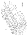
図3は、以下に詳しく説明する通り単式(シンプレックス)送信フィルタや単式低域信号フィルタまたはブランチ10(図1)と単式受信フィルタや単式高域信号フィルタまたはブランチ400(図12)とが並列の関係で適切に結合された、本発明の複式フィルタ800の1つの実施例を示す。
FIG. 3 illustrates a simplex transmit filter, single lowpass signal filter or branch 10 (FIG. 1) and a single receive filter, single highpass signal filter or branch 400 (FIG. 12) in parallel as described in detail below. FIG. 6 illustrates one embodiment of a
図1に示す通り、複式フィルタ800の送信フィルタ10は、好適な誘電定数のセラミック誘電物質を材料とする概略細長い形状、平行6面体または箱形の頑丈なブロックまたはコア12を具備する。ある実施例では、誘電材料は37以上の誘電定数のバリウムセラミックやネオジムセラミックの場合がある。
As shown in FIG. 1, the
コア12は、縦上面14、上面14と平行し正反対になる縦下面16(図4)、1番目の縦側面18、1番目の縦側面18と平行し正反対になる2番目の縦側面20(図4)、3番目の横側面または端面22および3番目の横側面または端面22と平行し正反対になる4番目の横側面または端面24という概略長方形の6つの面を含有する外面を規定する。
The
また、コア12は、上面14の4つの各外周辺端部から上方外側に延びる概略平面の4つの壁110、120、130および140を規定する。そして、壁110、120、130および140は協働して上部周辺フィルタリム200を規定し、壁110、120、130、140および上面14はフィルタ10上部のキャビティ150を規定する。
The
縦に延びる壁110と120は、相互に平行し正反対になる。横に延びる壁130と140は相互に平行し正反対になり、通常、壁110と120に垂面の関係で結合される。
The vertically extending
壁110は、外面111(図4)と内面112を含有する。外面111は、側面20(図4)と共に延び、同一平面上にある。壁110の中心部110Cは、上面14と壁110に対し約45°の角度で対向壁120の方向にリム200から上面14まで外側下方へ傾斜すなわち勾配する内面112Cを含有する。壁120、130および140のすべては、各コア側面と概略同一平面上にある概略垂直の外壁および上面14により規定される水平面と概略実質的に垂面の関係にある概略垂直の内壁を規定する。
また、壁110は、概略平行で離間した複数の壁部を規定する。端壁部110Aは、壁130に隣接し垂面に規定される。上方に延び隔離された接地壁、ポストまたはフィンガー110Bは、壁部110Aに隣接し離間した位置に規定される。スロット160は、端壁部110Aとポスト110Bの間に規定される。中央壁部110Cは、ポスト110Bに隣接、離間して位置する。スロット162は、ポスト110Bと中央壁部110Cの間に規定される。上方に延び隔離された接地壁、ポストまたはフィンガー110Dは、中央壁部110Cに隣接、離間して規定される。スロット164は、中央壁部110Cとポスト110Dの間に規定される。ポスト110Dはポスト110Bと正反対になり、壁140に隣接する壁110の端部に規定される。壁部110Eは、壁140とポスト110Dの間に規定される。壁部110Eは、壁140に対し垂面となる。スロット166は、ポスト110Dと壁部110Eの間に規定される。
The
また、壁110の内面112は、内垂直部112Aと112Bおよび内勾配面部または傾斜面部112C、112D、112Eを含む複数の部分に分離される。内面部112Aは、壁部110Aに位置する。内面部112Bは、壁部またはポスト110Bに位置する。内面部112Cは、壁部110Cに位置する。内面部112Dは、壁部またはポスト110Dに位置する。内面部112Eは、壁部110Eに位置する。
Further, the
また、壁部110C、110Dおよび110Eは、一般に三角形の側壁を規定する。具体的には、壁部110Cはポスト110Bから離間した側壁114Dおよびポスト110Dから離間した側壁114Eを規定する。ポスト110Dは、壁部110Cから離間した側壁114Fおよび壁部110Eから離間した側壁114Gを規定する。壁部110Eは、ポスト110Dから離間した側壁114Hを規定する。
The
壁120は、外面121と内面(図示なし)を含有する。外面121はコア側面18と共に延び、同一平面上にあり、内面(図示なし)はコア上面14に対し垂面である。
The
壁130は、外面131と内面(図示なし)を含有する。外面131はコア側面24と共に延び、同一平面上にあり、内面(図示なし)はコア上面14に対し垂面である。
壁140は、外面(図示なし)と内面142を含有する。外面(図示なし)はコア側面22と共に延び、同一平面上にあり、内面142はコア上面14に対し垂面である。
上方に延び隔離された壁部、ポストまたはフィンガー300は、コア側面18と24を橋渡しするコア12の左下隅に規定される。ポスト300は壁120と130から離間し、ポスト300と壁130の間のスロット302およびポスト300と壁120の間のスロット304を規定する。下に詳しく説明する通り、ポスト300は、金属化されない非金属化領域44と連続の1対の一般に三角形の側壁308を規定する。外側壁308は、コア側面18および壁120の外面121と同一平面上にある。ポスト300は、金属化上部リム312、コア端面24と壁130の外面131と同一平面上にある金属化前面306および金属化内勾配面または内斜面310を含有する。
An upwardly extending and isolated wall, post or
また、単式送信フィルタ10は、誘電体コア12に規定されコア12の上面14(図1)と下面16(図4)に終端がある複数の金属化スルーホール30により一部が規定される複数の共振器25を有する。スルーホール30は、コア側面22に隣接する点から対向コア側面24に隣接する点までブロック12に沿って離間した共直線の関係で延びる。各スルーホール30は、円筒形の金属化内側壁面32により規定される。
In addition, the
また、コア12の上面14は、導電金属化領域またはパターンと絶縁非金属化領域またはパターンとから成る凹型の表面層パターン40を規定する。パターン40の一部はコア12の上面14に規定され、キャビティ150底部の凹型位置に基づいてコア壁110、120、130および140の上部リム200から離間した関係で凹型フィルタパターンを規定する。
The
金属化領域は、導電銀を含有する材料の表面層の場合がある。また、凹型パターン40は、コア下面16、すべてのコア側面および各スルーホール30の側壁32を覆い共振器スルーホール内部から連続してコア上面14とコア下面16の両方へ延びる広い金属化領域またはパターンを規定する。この凹型パターンは、帯域外信号の送信を吸収または防止する役割を果たすため接地電極とも呼ばれる。
The metallized region may be a surface layer of a material containing conductive silver. The
コア上面14の凹型パターン40は少なくても共振器パッド60A、60B、60C、60D、60Eおよび60Fを有し、それらのパッドが少なくても部分的に各スルーホール30の上部開口部を囲繞する。共振器パッド60A〜Fはスルーホール30の各内面32を通じて延びる金属化領域に隣接または接続し、隣接する共振器および他の表面層金属化領域との容量結合を事前に設定する形状である。非金属化領域またはパターン44は金属化共振器パッド60A〜Fのすべてを囲繞し、コア側面18、20および24の少なくても一部に渡り延び、コア上面スロット部182、183、320および322へ延び、コア側壁部114E、114F、114Gおよび114Hへ延び、また、ポスト300の外側壁308の外側へ延びる。
The
また、非金属化領域44は、ポスト300の前面306とスロット302の下に位置するコア側面24の一部へ延びる一般に長方形の非金属化領域314を規定する。一般に長方形のもう1つの非金属化領域316は領域314と結合され、ポスト300の外側壁308とスロット304の下に位置するコア側面18の一部へ延びる。
The
同様の一般に長方形の非金属化領域317(図4)は、ポスト110Dおよびスロット164と166の上に位置するコア側面20の一部へ延びる。
A similar generally rectangular non-metallized region 317 (FIG. 4) extends to a portion of the
また、コア上面14の表面層パターン40は、1対の隔離された導電金属化信号領域、入出力送信接続領域または電極210およびアンテナ入出力信号接続領域または電極330を規定する。
Also, the
入出力信号接続領域210は壁110の一部、具体的にはRF信号入出力ポスト110Dの内面と上部リム部112及び200へ延び、下に詳しく説明する通り例えば表面実装送信導電接続点、パッドまたは接触部を規定する。
The input / output
金属化接続領域または電極210は、壁140に隣接して位置する。入力接続領域または電極210は、電極部211、212、213および214を含有する。電極部211は共振器パッド60Eと60Fの間に位置し、ポスト110Dの内面部112Dに位置する電極部212と接続する。電極部213は、電極部211と212に接続する。電極部214は、ポスト110Dの上部リム部200に位置する。また、電極部214は、ポスト110Dの外面に位置する電極部(図示なし)と接続する。さらに、電極部214は、非金属化領域により四方を囲繞されている。
A metallized connection region or
アンテナ接続領域330はポスト300へ延び、下に詳しく説明する通りアンテナ表面実装送信導電接続点、パッド、接触部またはポストとしての役割を果たす。
The
金属化アンテナ接続領域または電極330は概略L型で、壁120に隣接して位置する。電極330は、電極部331、332、333、334および335を含有する。電極部332は共振器パッド60Aと60Bの間に位置し、電極部331と接続する。電極部333はポスト300の内面部310に位置し、電極部331と接続する。電極部334はポスト300の上部リム部200に位置し、電極部333と接続する。電極部335はポスト300の外面306に位置し、非金属化領域により四方を囲繞されている。
The metallized antenna connection region or
凹面パターン40は、金属化領域と非金属化領域を含有する。非金属化領域は相互から離間し、それにより容量結合される。容量結合の量は、金属化領域のサイズや隣接する金属化部の間の分離距離ばかりでなく全体的なコア形状やコア誘電材料の誘電定数とほぼ関係する。同様に、面パターン40は、金属化領域間の誘導結合を引き起こす。
The
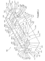
図2の説明に移るが、単式受信フィルタ400は、好適な誘電定数のセラミック誘電物質を材料とする概略細長い平行6面体または箱形の頑丈なブロックまたはコア412を具備する。ある実施例では、誘電材料は37以上の誘電定数のバリウムセラミックやネオジムセラミックの場合がある。
Turning to the description of FIG. 2, the single receive
コア412は、コア縦上面414、コア上面414と平行し正反対になるコア縦下面416(図4)、1番目のコア縦側面418、側面418と平行し正反対になる2番目のコア縦側面420、3番目のコア横側面または端面424およびコア端面424と平行し正反対になる4番目のコア横側面または端面422という概略長方形の6つの面を含有する外面を規定する。
The
また、コア412は、コア上面414の4つの各外周辺端部から上方外側に延びる概略平面の4つの壁510、520、530および540を規定する。そして、壁510、520、530および540のすべては上部周辺フィルタリム600を規定し、壁510、520、530、540および上面414は協働してフィルタ400上部のキャビティ550を規定するように結合する。縦壁510と520は、相互と平行し正反対になる。横壁530と540は相互と平行し正反対になり、壁510と520に概略垂面の関係で結合される。
The
壁510は、外面511と内面512を含有する。外面511はコア側面418と共に延び、同一平面上にあり、内面512の一部はコア上面414と壁510に対し約45°の角度で対向壁520の方向にリム600からコア上面414まで外側下方へ傾斜すなわち勾配する。壁520、530および540のすべては、各コア側面420、424、422と概略同一平面上にある概略垂直の外壁およびコア上面414により規定される水平面と通常ほぼ垂面の関係にある概略垂直の内壁を規定する。
また、壁510は、概略平行で離間した複数のスロット560、562、564および566を規定する。
The
端壁部510Aは、壁530とスロット560の間に規定される。端壁部510Aは、壁530に対し垂面である。隔離された接地壁、ポストまたはフィンガー510Bは壁部510Aに隣接、離間して位置し、それらの間のスペースがスロット560を規定する。中央壁部510Cはポスト510Bに隣接、離間して位置し、それらの間のスペースがスロット562を規定する。隔離された壁部、ポストまたはフィンガー510Dは中央壁部510Cに隣接、離間して位置し、それらの間のスペースがスロット564を規定する。ポスト510Dは、ポスト510Bと正反対になる。端壁部510Eはポスト510Dに隣接、離間して位置し、それらの間のスペースがスロット566を規定する。ポスト510Bと510Dは、フィルタ400のコア上面414から概略垂面の関係で外側上方に延びる。
End wall 510A is defined between
壁510のうち選択された内面部が、勾配または傾斜している。内勾配面部512Cは、壁部510Cに位置する。内勾配面部512Dは、壁部またはポスト510Dに位置する。内勾配面部512Eは、壁部510Eに位置する。
A selected inner surface of the
また、壁部510C、510Dおよび510Eは、概略三角形の側壁を規定する。具体的には、壁部510Cはポスト510Bに隣接する側壁514Dおよびポスト510Dに隣接する対向側壁(図示なし)を規定する。ポスト510Dは、壁部510Cに隣接する側壁514Fおよび端壁部510Eに隣接する側壁514Gを規定する。壁部510Eは、ポスト510Dに隣接する側壁514Hを規定する。
Further, the
壁520は、外面(図示なし)と内面522を含有する。外面(図示なし)はコア側面420と共に延び、同一平面上にあり、内面522はコア上面414に対し垂面である。
壁530は、外面531と内面(図示なし)を含有する。外面531はコア側面424と共に延び、同一平面上にあり、内面(図示なし)はコア上面414に対し垂面である。
壁540は、外面(図示なし)と内面542を含有する。外面(図示なし)はコア側面422と共に延び、同一平面上にあり、内面542はコア上面414に対し垂面である。
Wall 540 includes an outer surface (not shown) and an
隔離された壁部、ポストまたはフィンガー700は、各壁520と530に隣接し離間する関係でコア412の左上隅に規定される。ポスト700と壁530の間のスペースは、スロット702を規定する。ポスト700と壁520の間のスペースは、スロット704を規定する。下に詳しく説明する通り、ポスト700は、金属化されないコア上面414の非金属化領域444に連続する1対の概略三角形の側壁709を規定する。ポスト700は、金属化上部リム712、コア側面424と壁530の外面531と同一平面上にある金属化前面706および金属化内勾配面または内斜面710を含有する。ポスト700は、通常、フィルタ上面414から概略垂面に上方外側に延びる。ポスト700の外面709は、コア側面420および壁520の外面(図示なし)と同一平面上にある。
An isolated wall, post or
受信フィルタ400は、誘電体コア412に規定される複数のスルーホール430により部分的に規定される複数の共振器425を含有する。スルーホール430は、コア上面414と下面416に規定される各開口部から延び各開口部に終端がある。スルーホール430は、離間した共直線の関係でブロック412の縦軸に沿って延びる。各スルーホール430は、円筒形の金属化内側壁面432により規定される。
The
また、コア412の上面414は、導電金属化領域またはパターンと絶縁非金属化領域またはパターンとから成る凹型の表面層パターン440を規定する。パターン440の一部はコア412の上面414に規定され、キャビティ550底部の凹型位置により壁510、520、530および540の上部リム600から離間した関係で凹型フィルタパターンを規定する。
The
金属化領域は、導電銀を含有する材料の表面層の場合がある。また、凹型パターン440は、上面414、下面416、側面418、420、422、424およびスルーホール430の内壁432を覆い、共振器スルーホール内部から連続して上面414と下面416の両方へ延びる広い金属化領域またはパターンを規定する。この凹型パターンは、帯域外信号の送信を吸収または防止する役割を果たすため接地電極とも呼ばれる。
The metallized region may be a surface layer of a material containing conductive silver. The
コア上面414の凹型パターン440は複数の共振器パッド460A、460B、460C、460D、460Eおよび460Fから成り、それらのパッドは少なくても部分的にコア上面414に規定されるスルーホール430の各上部開口部を囲繞する。共振器パッド460A〜Fはスルーホール430の各内面432を通じて延びる金属化領域に連続または接続し、隣接する共振器および他の表面層金属化領域と所定の容量結合を有する形状にされる。
The
非金属化領域またはパターン444は、コア上面414の部分およびコア側面418、420および424の少なくても一部に渡り延びる。また、コア上面414の非金属化領域444は、金属化共振器パッド460A〜Fのすべてを囲繞する。さらに、非金属化領域444は上面スロット部582、583、720、722および側壁部514E、514F、514G、514H、709へ延び、少なくてもそれらを覆う。
The non-metallized region or
また、非金属化領域444は、ポスト700の前面706とスロット702の下に位置するコア側面424の一部へ延びる概略長方形の非金属化領域714を規定する。概略長方形のもう1つの非金属化領域(図示なし)は非金属化領域714と結合され、ポスト700の外側壁708とスロット704の下に位置するコア側面420の一部へ延びる。
The
同様の概略長方形の非金属化領域448は、ポスト510Dの前面およびスロット564と566の下に位置するコア側面418の一部へ延びる。
A similar generally rectangular
また、コア上面414の表面層パターン440は、入出力受信接続領域を含有する1対の隔離された導電金属化接合領域または電極610およびアンテナ入出力信号接続領域または電極730を規定する。
Also, the
受信接続領域610は壁510と側面418の一部、具体的にはポスト510Dの内面部及びリム部512D及び600へ延び、下に詳しく説明する通り表面実装受信導電接続点、パッド、接触部またはポストを規定する。
The receive
電極610は、壁540に隣接する上面414に位置する。接続領域または電極610は、電極部611、612、614および615を含有する。電極部611は共振器パッド460Eと460Fの間に位置し、ポスト510Dの内面部512Dに位置する電極部612と接続し、電極部611と接続する。電極部614はポスト510Dのリム600に位置し、電極部612と接続する。電極部615はポスト510Dの外面に位置し、電極部614と接続し、非金属化領域により四方を囲繞されている。
The
アンテナ接続領域730はポスト700へ延び、下に詳しく説明する通り表面実装導電アンテナ接続点、パッド、接触部またはポストを規定する。
The
金属化アンテナ接続領域または電極730は概略L型で、壁530に隣接するコア上面414に位置する。接続領域または電極730は、電極部731、732、733、734および735を含有する。電極部732は共振器パッド460Aと460Bの間に位置し、電極部731と接続する。電極部733はポスト700の内面部710に位置し、電極部731と接続する。電極部734はポスト700の上部リム部600に位置し、電極部733と接続する。電極部735はポスト700の外面706に位置し、電極部734と接続する。電極部735は、非金属化領域により四方を囲繞されている。
The metalized antenna connection region or
凹面パターン440は、金属化領域と非金属化領域を含有する。金属化領域は相互から離間し、それにより容量結合される。容量結合の量は、金属化領域のサイズや隣接する金属化部の間の分離距離ばかりでなく全体的なコア形状やコア誘電材料の誘電定数とほぼ関係する。同様に、面パターン440は、金属化領域間の誘導結合を引き起こす。
図3の説明に移るが、単式低域フィルタまたは単式送信フィルタ10は単式高域フィルタまたは単式受信フィルタ400に連結または接合され、本発明の複式フィルタ800の1つの実施例を形成する。
Turning to FIG. 3, the single low pass filter or single transmit
フィルタ10と400は、様々な方法により結合できる。例えば、各フィルタ10と400のコア縦側面18と420は金属材料で覆われており、フィルタ10と400、具体的には、それらの各側面18と420および壁120と520を並列および隣接の関係で結合し、次にフィルタ10と400を炉で熱してフィルタ10の側面18の外面の金属およびフィルタ400の側面420の外面の金属を焼結、融合することにより単一の金属化フィルタ内壁805を中央に形成して両方のフィルタを結合できる。内壁805は、1番目の組のスルーホール830Aと2番目の組のスルーホール830Bとの間を複式フィルタ800の全中心に沿って縦に延びる接地板を形成、規定し、これにより、これらを好適に分離、隔離することができる。フィルタ10と400を結合するためには、導電性エポキシ樹脂、はんだ、または機械結合の技術を利用しても良い。
ある実施例では、複式フィルタは個々の別々の単式フィルタ10と400の組合せから成り、各フィルタ10と400のコア12と412により規定される概略細長い平行6面体または箱形の頑丈なブロックまたはコア812を具備する。コア812は、各フィルタ10と400の結合縦上面14と414により規定される縦上面814、各フィルタ10と400の結合縦下面16と416により規定されコア上面814と平行し正反対になる縦下面816(図4)、フィルタ400の縦側面418により規定される1番目の縦側面818、フィルタ10の側面20により規定されコア側面818と平行し正反対になる2番目の縦側面820(図4)、各フィルタ10と400の結合側面22と422により規定される3番目の横側面または端面822(図3と4)および各フィルタ10と400の結合側面24と424により規定され端面822と平行し正反対になる4番目の横側面または端面824という概略長方形の6つの面を含有する外面を規定する。コア面822と824は、コア面818と820に対し垂面である。フィルタ内壁805は、コア面818と820に平行である。
In one embodiment, the duplex filter consists of a combination of individual separate
また、コア812は、フィルタ10の壁110により規定される縦壁810、810と反対になりフィルタ400の壁510により規定される縦壁820、各フィルタ10と400の結合壁130と530により規定される横側壁830および830と反対になり各フィルタ10と400の結合壁140と540により規定される横側壁840という、上面814の4つの各外周辺端部から上方外側に延びる概略平面の4つの壁を規定する。
The core 812 is defined by the vertical wall 820 defined by the
壁810、820、830および840は協働して上部周辺リム1000を規定し、また、壁810、820、830、840およびコア上面814は上部のキャビティ850を規定する。壁810と820は、相互に平行し正反対になる。壁830と840は相互に平行し正反対になり、壁810と820に概略垂面の関係で結合される。
縦壁810は離間、隔離された1対のポストまたはフィンガー1010Bと1010Dを規定し、それらのポストはフィルタ10の各ポストまたはフィンガー110Bと110Dにより規定され位置、構造および機能が一致する。以上の説明は、参照用として本書に援用する。ポスト1010Bは壁830に隣接して位置し、ポスト1010Dは壁840に隣接して位置する。
The vertical wall 810 defines a pair of spaced apart and isolated posts or fingers 1010B and 1010D, which are defined by each post or finger 110B and 110D of the
対向縦壁820は離間、隔離された1対のポストまたはフィンガー1510Bと1510Dを規定し、それらのポストはフィルタ400の各ポストまたはフィンガー510Bと510Dにより規定され位置、構造および機能が一致する。以上の説明は、参照用として本書に援用する。ポスト1510Bは壁830に隣接して位置し、ポスト1010Bと正反対になる。ポスト1510Dは壁840に隣接して位置し、ポスト1010Dと正反対になる。
Opposing vertical wall 820 defines a pair of spaced apart, isolated posts or
横縦壁830は隔離され概略中心に位置するポストまたはフィンガー1210を規定し、そのポストは各フィルタ10と400のポストまたはフィンガー300と700の結合、具体的には隣接した関係にある各外面308と709の結合により規定される。
The transverse
また、フィルタ800は、各フィルタ10と400の結合壁120と520により規定され壁840から対向壁830の手前までフィルタ800の中心を縦方向に延びる中心の縦内壁842を含有する。壁842は、壁810と820に平行で離間した関係でフィルタ800のコア上面814から上方外側に延びる。また、壁842は、フィルタ上面814とキャビティ850を概略長方形の上部と下部を有する概略平行に隣接する送受信フィルタ部またはキャビティ852と854に分割、隔離する。
The
キャビティまたは部位852は各フィルタ壁810と842の間に規定され、キャビティまたは部位854は各フィルタ壁854と842の間に規定される。
A cavity or
部位852は、フィルタ10の共振器25、スルーホール30およびパターン40により規定され、位置、構造および機能が対応し、したがって、参照によりここに組み込まれる複数の共振器スルーホール830Aにより部分的に規定される複数の共振器825Aと、導電金属化領域またはパターンと絶縁非金属化領域またはパターンとから成るパターン840Aとをコア上面814に含有する。
スルーホール830Aは、中心の内壁842上のこれと平行なブロックまたはコア812のコア上面814に沿って離間した平行の関係で縦に延びる。各スルーホール830Aはコア812を通じて延び、コア812の上面814と下面816により規定される各開口部に終端がある。
The through-hole 830A extends vertically in a parallel relationship spaced along the core
フィルタ800のパターン840A、ポスト1010Dおよびポスト1210の各々は、パターン40の各導電材料ストリップ211、212、214、330、333および312により規定され、位置、構造および機能が対応し、したがって、参照によりここに組み込まれる各導電材料ストリップ1211、1212、1214、1330、1333および1312、ポスト110Dならびにフィルタ10のポスト300の各々を含有する。
Each of pattern 840A, post 1010D, and post 1210 of
部位854は、フィルタ400の共振器425、スルーホール430およびパターン440により規定され、位置、構造および機能が対応し、したがって、参照によりここに組み込まれる共振器スルーホール830Aと並行し正反対になる複数の共振器スルーホール830Bにより部分的に規定される複数の共振器825Bと、導電金属化領域またはパターンと絶縁非金属化領域またはパターンとから成るパターン840Bとをコア上面814に含有する。
The
スルーホール830Bは、中心の内壁842とスルーホール830Aの下でこれと平行にブロックまたはコア812に沿って離間した平行の関係で縦に延びる。各スルーホール830Bはコア812を通じて延び、コア812の上面814と下面816により規定される各開口部に終端がある。
The through hole 830B extends vertically in a parallel relationship spaced along the block or core 812 below and parallel to the central
フィルタ800のパターン840B、ポスト1510Dおよびポスト1210の各々は、パターン440の各導電材料ストリップ611、612、614、730、733および734により規定され、位置、構造および機能が対応し、したがって、参照によりここに組み込まれる各ストリップ1611、1612、1614、1730、1333および1334、ポスト510Dならびにフィルタ400のポスト700の各々を含有する。
Each of pattern 840B, post 1510D, and post 1210 of
また、パターン840Aと840Bは、各コア側面818、824および820の非金属化領域1448、1714および1715を除いて、フィルタ外面810、820、822および824、各壁810、820、830、840および842の外部、内部およびリムならびに各共振器スルーホール830Aと830Bの内部を覆う金属化層を含有する。各非金属化領域1448、1714および1715は、各ポスト1510D、1210および1010Dの下に位置する。
Patterns 840A and 840B also include filter
このように、図3の実施例では、送信接続フィンガー、ポスト、パッドまたは電極1010Dはフィルタ800の縦壁810に位置し、受信接続フィンガー、ポスト、パッドまたは電極1510Dはパッド1010Dに正反対の関係でフィルタ800の縦壁820に位置し、アンテナ接続フィンガー、ポスト、パッドまたは電極1210は壁810と820を結合する横壁830に位置する。
Thus, in the embodiment of FIG. 3, the transmit connection finger, post, pad or electrode 1010D is located on the vertical wall 810 of the
また、中心の内壁842は、各送受信フィルタ部852と854、各金属化上面パターン840Aと840Bおよび各スルーホール825Aと825Bを隔離、分離することが分かる。
Further, it can be seen that the central
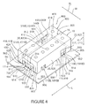
図4の説明に移るが、複式フィルタ800が概略平面で長方形の回路基板(PCB)900に取り付けられた様子を示している。ある実施例では、回路基板900は、上面902、下面(図示なし)および複数の側面903、904、905、906を含有するプリント回路基板である。回路基板900の板厚BHは、PCB上面902と下面(図示なし)の間の面906に沿って測定される。また、回路基板900は、PCB上面と下面の間の電気接続部となるめっきスルーホール925を含有する。複数の回路線910と接続パッド912は上面902に位置し、端子914と接続される。回路線910、接続パッド912および端子914は、銅などの金属を材料とする。端子914は、複式フィルタ800を外部電気回路(図示なし)に接続する。
Turning to the description of FIG. 4, the
複式フィルタ800は上面を下向きにしてPCB900に取り付けられ、コア上面814はPCB900の上面902と向かい合い平行で離間した関係となり、フィルタ800の壁810、820、830、840および842により規定されるリム1000はPCB900の上面902に設置、はんだ付けされる。この関係では、フィルタ800により規定されるキャビティ850が部分的にシールされ、上面814、基板面902および壁810、820、830、840、842により規定される囲いを規定する。
The
また、この関係では、複式フィルタ800の概略垂直で細長いスルーホール830Aと830BはPCB900に対し通常ほぼ垂直の関係で規定、配置され、各スルーホール825Aと825Bの開口部は基板上面902と向かい合い離間した関係となる。
Also, in this relationship, the substantially vertical and elongated through holes 830A and 830B of the
図4の結合関係では、アンテナ接続ポスト、パッドまたは電極1210、具体的にはリム1000の金属化リム部1312と1334は、はんだ920によりPCB900の金属化接続パッド912の1つに設置、結合される。同様に、送信ポストまたはパッド1010D、具体的には金属化リム部1214は、はんだ920によりPCB900の接続パッド912の別の1つに設置、結合される。さらに、受信ポストまたはパッド1510D、具体的には金属化リム部1614は、同様に基板上面902の接続パッド912の別の1つに設置、結合される。そして次に、各接続パッド912が各回路線910に結合される。
4, the antenna connection post, pad or
フィルタ800の対向縦面にある送信入力接続パッド1010Dと受信出力接続パッド1510Dの位置は干渉とクロストークを減少させる利点があり、また、各送信入力・受信出力回路線910も基板900の対向縦面903と906に位置させることを可能にし、これにより、より良い隔離を形成し、各回路線間の干渉を減少させることができる。
The positions of the transmission input connection pad 1010D and the reception
また、回路基板900は、概略長方形の接地リングまたは接地線930を上面902に含有する。接地リングまたは接地線は銅を材料とし、はんだ935(一部のみを図4に示す)により各電極とフィルタ壁のリムがその上に付着される。例えば、最初にはんだ920と935により接地リング930と接続パッド912の各々が覆われ、次に電極部1010Dと1210が各接続パッド912と一致するように複式フィルタ800が上面902に設置される。そして、回路基板900と複式フィルタ800がリフロー炉に入れられ、はんだ920と935が溶融、リフローされる。
The
各壁810、810、830、840および842のリム1000の接地リング930への取り付けは、複式フィルタ800の外面の大部分を接地するための電気路を形成する。
The attachment of each
図4に示す通り、複式フィルタ800の寸法は長さL、幅W、高さHおよびHに等しい共振器長さRLである。典型的には1.0GHzで動作する高周波フィルタの場合、複式フィルタ800の設計では共振器長さ(RL)を基板高さ(BH)以下にする必要がある場合がある。下面を基板に平らに設置するか(上面を上向きにして)、側面の1つを基板に平らに設置する(上面を横向きにして)ことにより取り付ける従来技術のフィルタでは、共振器長さが基板高さより短くなる場合、フィルタは回路基板に取り付けられる際に高周波で不安定になる場合がある。余分な電磁場が生成され、フィルタの減衰が妨害されたり低下する場合もある。また、これらの余分な電磁場は、ゼロ点としても知られるフィルタポールの減衰と減衰の鋭さを低下させる場合もある。
As shown in FIG. 4, the dimensions of the
基板900と向かい合う面814に凹型上面パターン840Aと840Bを具備した本発明の複式フィルタ800を使用することにより、接地と帯域外信号の吸収が改善され、電磁場がキャビティ850内部に閉じ込められ、フィルタの減衰とゼロ点の改善するように、キャビティ850外部の電磁場がノイズや干渉を生じさせることが防がれる。
By using the
本発明では、同じ設置面積(長さLと幅W)を複数の周波数帯域について使用できる。従来技術のフィルタでは、典型的には、フィルタ目標の周波数に応じてサイズまたは設置面積を増減させる必要がある。フィルタ800は同じ設置面積を有して様々な周波数で使用できる。
In the present invention, the same installation area (length L and width W) can be used for a plurality of frequency bands. Prior art filters typically require an increase or decrease in size or footprint depending on the filter target frequency. The
本発明の別の利点としては、はんだリフローの過程でのフィルタ800とPCB900の設置リング930の自己整合を挙げられる。液状はんだ935の表面張力は、リフローの過程で設置リング930間のリムおよびコア812の自己センタリング機能を提供するリムの周りに等しく分散されるため、フィルタ800は優れた自己整合を示す。
Another advantage of the present invention is the self-alignment of the
また、複式フィルタ800では壁810、820、830、840、842および基板900が遮蔽機能を果たすため、スプリアスの電磁妨害を減少させるために現在使用されている外部の金属遮蔽材などの遮蔽材を設置する必要がなくなる。しかし、特別な用途の場合には、遮蔽材を適宜、フィルタ800に付加することもできる。
In the
また、本発明では、接地が改善されて電磁場がキャビティ850内部に閉じ込められるため、より急峻な減衰を示すフィルタ800が提供される。キャビティ内壁842を使用する結果として、フィルタ800の各送受信部において金属化パターンと共振器パッドの隔離が改善され、従来のフィルタと比較して高調波抑制を改善できる。
The present invention also provides a
また、本発明では、入力電極、出力電極およびアンテナ電極をフィルタ800の端部または壁に沿って配置することが可能になる。図には示していないが、ある実施例では、アンテナ電極をフィルタの送信入力電極やパッドまたは受信出力電極やパッドと同じ側壁に設置することも可能である。従来技術の表面実装フィルタでは、すべての電極が誘電体ブロックと同じ面にあることが要求される。
In the present invention, the input electrode, the output electrode, and the antenna electrode can be disposed along the end portion or wall of the
また、凹型パターン840Aと840Bにより、直列に接地に接続されたキャパシタンスとインダクタンスを含む共振器回路が実現する。パターン840Aと840Bの形状により、全体的なキャパシタンス値とインダクタンス値が決定される。キャパシタンス値とインダクタンス値は、通過帯域の整数間隔の調和振動数などの通過帯域外周波数に対する周波数応答を抑制する共振器回路を形成できるように設計される。 Further, the concave patterns 840A and 840B realize a resonator circuit including a capacitance and an inductance connected in series to the ground. The overall capacitance and inductance values are determined by the shape of the patterns 840A and 840B. The capacitance value and the inductance value are designed so as to form a resonator circuit that suppresses a frequency response to frequencies outside the passband such as harmonic frequencies of integer intervals in the passband.
図の実施例では上面814に隣接したキャビティ850が示されているが、キャビティおよびキャビティを規定する対応壁はフィルタの単数または複数の他の面に形成できることも分かる。
Although the illustrated embodiment shows a
別の実施例では、キャビティ850がコア812の面の一部のみを覆う場合もある。例えば、キャビティ850は上面814の10%のみを包含する場合がある。別の実施例では、複数のキャビティが対応する増設壁によりコア812の同じ側または面に配置、形成される場合もある。
In another example, the
また、本発明では、標準的な単式フィルタを結合するだけで複式フィルタ800を形成できるため、製造工程を簡易化しコストを削減できるという利点がある。
Further, in the present invention, since the
マイクロウェーブオフィスコンピュータシミュレーションソフトウェアを使用したコンピュータシミュレーションにより、長さ16.17mm、高さ5.1mm、幅9.04mmの複式フィルタ800を評価した。フィルタ性能シミュレーションのパラメータを下の表1に示す。

図5は本発明の複式フィルタ800の性能シミュレーションによる信号強度(または信号損失)対周波数を示すグラフであり、低域通過域または送信帯域は880〜915MHz、広域通過帯域または受信帯域は925〜960MHzである。複式フィルタ800の受信ポートと送信ポート間のピークアイソレーション(S23)は918MHzで−35.7dBであり、従来技術の複式フィルタと比較して改善されている。複式フィルタ800のS12値は送信帯域端部において915MHzで−45dBであり、S13値は受信帯域端部において927MHzで−59dBである。
FIG. 5 is a graph showing signal strength (or signal loss) versus frequency according to the performance simulation of the
本発明は、様々な周波数で動作するRF信号フィルタに応用できる。主な応用例としては、携帯電話、携帯電話基地局、加入者ユニットなどを挙げられる。その他の高周波応用例としては、衛生通信、グローバルポジショニングシステム(GPS)、マイクロ波応用技術などの通信デバイスを挙げられる。 The present invention can be applied to RF signal filters operating at various frequencies. Major applications include mobile phones, mobile phone base stations, subscriber units, and the like. Other examples of high frequency applications include communication devices such as sanitary communication, global positioning system (GPS), and microwave application technology.
上に説明した実施例は、本発明の新しい特長の精神と範囲から逸脱することなく様々な変形例が可能である。本書は、ここに説明する特殊フィルタの限定を意図、暗示していない。無論、添付の特許請求の範囲は、変形例もその範囲に網羅されることを意図している。 Various modifications can be made to the embodiments described above without departing from the spirit and scope of the new features of the present invention. This document is not intended or implied to limit the special filters described herein. Of course, the appended claims are intended to cover the modifications as well.
Claims (15)
前記上面から外側に延びる、少なくても1番目、2番目および3番目のポストと、
前記コア上の金属化領域と非金属化領域の表面層パターンであって、前記上面に位置し前記1番目のポストへ延びる1番目の金属化接続領域、前記上面に位置し前記2番目のポストへ延びる2番目の金属化接続領域および前記上面に位置し前記3番目のポストへ延びる3番目の金属化接続領域を含む前記パターンとを有するフィルター。 A core including an upper surface, a lower surface and side surfaces and defining a first and a second set of spaced through holes, wherein each through hole is defined in the lower surface from an opening defined in the upper surface Extending through the core to a portion, the core;
At least first, second and third posts extending outwardly from the top surface;
A surface layer pattern of metallized and non-metallized regions on the core, the first metallized connection region located on the top surface and extending to the first post; the second post located on the top surface And a second metallized connection region extending to and the pattern including a third metallized connection region located on the top surface and extending to the third post.
前記上面から外側に延びる複数の壁と、
前記上面に規定された前記壁の1つへ延びる入力電極、前記上面に規定された前記壁の1つへ延びる出力電極および前記上面に規定された前記壁の1つへ延びるアンテナ電極を含む前記ブロックの前記上面に規定される金属化領域と非金属化領域のパターンを有するフィルタ。 A block containing a top surface, a bottom surface and at least one side surface and defining first and second sets of through-holes extending between the openings defined in the top surface and the bottom surface;
A plurality of walls extending outward from the top surface;
An input electrode extending to one of the walls defined on the top surface; an output electrode extending to one of the walls defined on the top surface; and an antenna electrode extending to one of the walls defined on the top surface. A filter having a pattern of metallized areas and non-metallized areas defined on the top surface of the block.
前記コアを通じて延び前記外面の開口部に終端がある1番目と2番目の組のスルーホール、および
前記1番目と2番目の組のスルーホールの各開口部を分離する前記外面に形成される少なくても1番目の壁を有するフィルタ。 A core of dielectric material containing an outer surface having a metallized region pattern;
The first and second sets of through-holes extending through the core and terminating at the outer-surface openings, and the outer surfaces forming the first and second sets of through-holes are separated from each other. A filter with even the first wall.
Applications Claiming Priority (3)
| Application Number | Priority Date | Filing Date | Title |
|---|---|---|---|
| US20459409P | 2009-01-08 | 2009-01-08 | |
| US61/204,594 | 2009-01-08 | ||
| PCT/US2010/020393 WO2010080929A1 (en) | 2009-01-08 | 2010-01-07 | Duplex filter with recessed top pattern and cavity |
Publications (2)
| Publication Number | Publication Date |
|---|---|
| JP2012514954A true JP2012514954A (en) | 2012-06-28 |
| JP2012514954A5 JP2012514954A5 (en) | 2013-02-21 |
Family
ID=42200924
Family Applications (1)
| Application Number | Title | Priority Date | Filing Date |
|---|---|---|---|
| JP2011545435A Pending JP2012514954A (en) | 2009-01-08 | 2010-01-07 | Dual filter with concave top pattern and cavity |
Country Status (8)
| Country | Link |
|---|---|
| US (1) | US8294532B2 (en) |
| JP (1) | JP2012514954A (en) |
| KR (1) | KR20110102925A (en) |
| CN (2) | CN202839908U (en) |
| CA (1) | CA2749145A1 (en) |
| DE (1) | DE112010000694T5 (en) |
| GB (1) | GB2479108A (en) |
| WO (1) | WO2010080929A1 (en) |
Families Citing this family (12)
| Publication number | Priority date | Publication date | Assignee | Title |
|---|---|---|---|---|
| US9030275B2 (en) * | 2008-12-09 | 2015-05-12 | Cts Corporation | RF monoblock filter with recessed top pattern and cavity providing improved attenuation |
| US9030272B2 (en) * | 2010-01-07 | 2015-05-12 | Cts Corporation | Duplex filter with recessed top pattern and cavity |
| JP5703917B2 (en) * | 2011-04-08 | 2015-04-22 | 宇部興産株式会社 | Dielectric resonant component |
| CN104821422A (en) * | 2015-05-12 | 2015-08-05 | 庄昆杰 | Low-loss high-isolation miniaturized double-broadband combining dividing filter |
| RU2636404C2 (en) * | 2016-02-24 | 2017-11-23 | Акционерное Общество "Специальное Конструкторско-Технологическое Бюро По Релейной Технике" (Ао "Сктб Рт") | Dual-band ceramic filter |
| CN109845027A (en) * | 2016-09-23 | 2019-06-04 | Cts公司 | Ceramic RF filter with the structure for stopping RF signal to couple |
| US10363622B2 (en) * | 2016-09-30 | 2019-07-30 | General Electric Company | Electrode for an electro-erosion process and an associated method thereof |
| US10587024B2 (en) | 2016-10-21 | 2020-03-10 | LGS Innovations LLC | Hermetic sealing of ceramic filters |
| US10587025B2 (en) | 2016-11-08 | 2020-03-10 | LGS Innovations LLC | Ceramic filter with window coupling |
| GB2558376A (en) * | 2016-11-09 | 2018-07-11 | Isotek Microwave Ltd | A ceramic dual mode microwave resonant filter and a multiplexer including such a filter |
| CN108172956B (en) * | 2017-11-16 | 2019-09-20 | 上海华为技术有限公司 | A kind of microwave combiner |
| KR102495987B1 (en) * | 2021-04-28 | 2023-02-06 | 서울시립대학교 산학협력단 | Monoblock ceramic waveguide duplexer |
Citations (6)
| Publication number | Priority date | Publication date | Assignee | Title |
|---|---|---|---|---|
| JPS6247201A (en) * | 1985-08-23 | 1987-02-28 | Murata Mfg Co Ltd | Shared dielectric block |
| JPS62104201A (en) * | 1985-10-30 | 1987-05-14 | Fujitsu Ltd | Dielectric filter |
| JPH02130103U (en) * | 1988-11-16 | 1990-10-26 | ||
| JPH06237104A (en) * | 1993-01-11 | 1994-08-23 | Matsushita Electric Ind Co Ltd | Filter device |
| JPH07176908A (en) * | 1993-12-16 | 1995-07-14 | Murata Mfg Co Ltd | Dielectric resonance component and its characteristic adjustment method |
| JP2000004103A (en) * | 1998-04-17 | 2000-01-07 | Murata Mfg Co Ltd | Dielectric filter, dielectric duplexer, their mount structure, and communication equipment |
Family Cites Families (39)
| Publication number | Priority date | Publication date | Assignee | Title |
|---|---|---|---|---|
| JPS60114004A (en) * | 1983-11-25 | 1985-06-20 | Murata Mfg Co Ltd | Dielectric coaxial resonator |
| JPS614303A (en) * | 1984-06-19 | 1986-01-10 | Nec Corp | Dielectric band pass filter |
| JPS61258502A (en) * | 1985-05-10 | 1986-11-15 | Murata Mfg Co Ltd | Microwave filter |
| JPH055681Y2 (en) * | 1985-10-18 | 1993-02-15 | ||
| US4837534A (en) * | 1988-01-29 | 1989-06-06 | Motorola, Inc. | Ceramic block filter with bidirectional tuning |
| US5227747A (en) * | 1989-06-15 | 1993-07-13 | Oki Electric Industry Co., Ltd. | Dielectric filter having coupling amount adjusting patterns |
| GB2234399B (en) * | 1989-06-21 | 1993-12-15 | Murata Manufacturing Co | Dielectric filter |
| US5144269A (en) * | 1990-03-20 | 1992-09-01 | Sanyo Electric Co., Ltd. | Dielectric filter having external connection formed on dielectric substrate |
| US5214398A (en) * | 1990-10-31 | 1993-05-25 | Ube Industries, Ltd. | Dielectric filter coupling structure having a compact terminal arrangement |
| JPH04242301A (en) | 1991-01-17 | 1992-08-31 | Matsushita Electric Ind Co Ltd | Dielectric filter |
| US5293141A (en) * | 1991-03-25 | 1994-03-08 | Sanyo Electric Co., Ltd. | Dielectric filter having external connection terminals on dielectric substrate and antenna duplexer using the same |
| US5191305A (en) * | 1991-07-02 | 1993-03-02 | Interstate Electronics Corporation | Multiple bandpass filter |
| US5177458A (en) * | 1991-07-31 | 1993-01-05 | Motorola, Inc. | Dielectric filter construction having notched mounting surface |
| JP2811382B2 (en) | 1991-12-11 | 1998-10-15 | 富士電気化学株式会社 | Dielectric filter |
| US5208566A (en) * | 1992-01-21 | 1993-05-04 | Motorola, Inc. | Dielectric filter having adjacently-positioned resonators of dissimilar cross-sectional dimensions and notched side surface |
| JPH05275905A (en) | 1992-03-25 | 1993-10-22 | Oki Electric Ind Co Ltd | Packaging structure of branching filter |
| JPH05315807A (en) * | 1992-05-08 | 1993-11-26 | Oki Electric Ind Co Ltd | Strip line filter and antenna multicoupler using the filter |
| JPH06132706A (en) * | 1992-09-07 | 1994-05-13 | Murata Mfg Co Ltd | Dielectric resonance parts |
| JPH06216607A (en) | 1993-01-18 | 1994-08-05 | Ube Ind Ltd | Dielectric filter and manufacture therefor |
| JP3230353B2 (en) * | 1993-11-18 | 2001-11-19 | 株式会社村田製作所 | Antenna duplexer |
| JP3307052B2 (en) * | 1994-02-17 | 2002-07-24 | 株式会社村田製作所 | Dielectric resonator device |
| US5512866A (en) | 1994-04-29 | 1996-04-30 | Motorola, Inc. | Ceramic duplex filter |
| US5602518A (en) * | 1995-03-24 | 1997-02-11 | Motorola, Inc. | Ceramic filter with channeled features to control magnetic coupling |
| JPH098506A (en) * | 1995-06-21 | 1997-01-10 | Matsushita Electric Ind Co Ltd | Band stop filter |
| JPH09219605A (en) * | 1996-02-09 | 1997-08-19 | Ngk Spark Plug Co Ltd | Dielectric filter and resonance frequency adjusting method therefor |
| US5731751A (en) * | 1996-02-28 | 1998-03-24 | Motorola Inc. | Ceramic waveguide filter with stacked resonators having capacitive metallized receptacles |
| US5793267A (en) * | 1996-03-07 | 1998-08-11 | Murata Manufacturing Co., Ltd. | Dielectric block filter having first and second resonator arrays coupled together |
| US6052040A (en) * | 1997-03-03 | 2000-04-18 | Ngk Spark Plug Co., Ltd. | Dielectric duplexer with different capacitive coupling between antenna pad and transmitting and receiving sections |
| US6081174A (en) | 1997-03-14 | 2000-06-27 | Taiyo Yuden Co., Ltd. | Wave filter having two or more coaxial dielectric resonators in juxtaposition |
| JPH10335906A (en) * | 1997-03-31 | 1998-12-18 | Murata Mfg Co Ltd | Dielectric filter, dielectric duplexer, and communication equipment device |
| US5959511A (en) * | 1998-04-02 | 1999-09-28 | Cts Corporation | Ceramic filter with recessed shield |
| JP3344333B2 (en) * | 1998-10-22 | 2002-11-11 | 株式会社村田製作所 | Dielectric antenna with built-in filter, dielectric antenna with built-in duplexer, and wireless device |
| JP2000295008A (en) * | 1999-02-03 | 2000-10-20 | Murata Mfg Co Ltd | Dielectric resonator device, dielectric filter, dielectric duplexer, and method for forming input-output electrode for communication equipment and dielectric resonator device |
| JP2001094304A (en) * | 1999-09-17 | 2001-04-06 | Tdk Corp | Dielectric filter and its manufacture |
| JP2002246806A (en) * | 2001-02-15 | 2002-08-30 | Murata Mfg Co Ltd | Dielectric filter and dielectric duplexer and communication equipment |
| JP3788384B2 (en) * | 2001-05-30 | 2006-06-21 | 株式会社村田製作所 | Dielectric filter, dielectric duplexer, and communication device |
| JP3317404B1 (en) * | 2001-07-25 | 2002-08-26 | ティーディーケイ株式会社 | Dielectric device |
| US6879222B2 (en) * | 2002-02-14 | 2005-04-12 | Cts Corporation | Reduced length metallized ceramic duplexer |
| JP5620273B2 (en) * | 2007-12-10 | 2014-11-05 | シーティーエス・コーポレーションCts Corporation | RF single block filter with recessed top pattern and cavity providing improved attenuation |
-
2010
- 2010-01-07 JP JP2011545435A patent/JP2012514954A/en active Pending
- 2010-01-07 KR KR1020117017821A patent/KR20110102925A/en not_active Application Discontinuation
- 2010-01-07 US US12/683,997 patent/US8294532B2/en active Active
- 2010-01-07 CN CN2012202056205U patent/CN202839908U/en not_active Expired - Fee Related
- 2010-01-07 WO PCT/US2010/020393 patent/WO2010080929A1/en active Application Filing
- 2010-01-07 DE DE112010000694T patent/DE112010000694T5/en not_active Withdrawn
- 2010-01-07 GB GB1113470A patent/GB2479108A/en not_active Withdrawn
- 2010-01-07 CN CN2010900006376U patent/CN202308233U/en not_active Expired - Fee Related
- 2010-01-07 CA CA2749145A patent/CA2749145A1/en not_active Abandoned
Patent Citations (6)
| Publication number | Priority date | Publication date | Assignee | Title |
|---|---|---|---|---|
| JPS6247201A (en) * | 1985-08-23 | 1987-02-28 | Murata Mfg Co Ltd | Shared dielectric block |
| JPS62104201A (en) * | 1985-10-30 | 1987-05-14 | Fujitsu Ltd | Dielectric filter |
| JPH02130103U (en) * | 1988-11-16 | 1990-10-26 | ||
| JPH06237104A (en) * | 1993-01-11 | 1994-08-23 | Matsushita Electric Ind Co Ltd | Filter device |
| JPH07176908A (en) * | 1993-12-16 | 1995-07-14 | Murata Mfg Co Ltd | Dielectric resonance component and its characteristic adjustment method |
| JP2000004103A (en) * | 1998-04-17 | 2000-01-07 | Murata Mfg Co Ltd | Dielectric filter, dielectric duplexer, their mount structure, and communication equipment |
Also Published As
| Publication number | Publication date |
|---|---|
| KR20110102925A (en) | 2011-09-19 |
| WO2010080929A1 (en) | 2010-07-15 |
| CN202308233U (en) | 2012-07-04 |
| DE112010000694T5 (en) | 2012-11-08 |
| CA2749145A1 (en) | 2010-07-15 |
| CN202839908U (en) | 2013-03-27 |
| GB2479108A (en) | 2011-09-28 |
| US8294532B2 (en) | 2012-10-23 |
| US20100141352A1 (en) | 2010-06-10 |
| GB201113470D0 (en) | 2011-09-21 |
Similar Documents
| Publication | Publication Date | Title |
|---|---|---|
| JP5620273B2 (en) | RF single block filter with recessed top pattern and cavity providing improved attenuation | |
| JP2012514954A (en) | Dual filter with concave top pattern and cavity | |
| US9030275B2 (en) | RF monoblock filter with recessed top pattern and cavity providing improved attenuation | |
| US7541893B2 (en) | Ceramic RF filter and duplexer having improved third harmonic response | |
| US8682403B2 (en) | Filter having impedance matching circuits | |
| US9030272B2 (en) | Duplex filter with recessed top pattern and cavity | |
| JP4291164B2 (en) | Surface acoustic wave device | |
| JP4365858B2 (en) | Low profile ceramic RF filter | |
| US9030276B2 (en) | RF monoblock filter with a dielectric core and with a second filter disposed in a side surface of the dielectric core | |
| US10587025B2 (en) | Ceramic filter with window coupling | |
| US6650202B2 (en) | Ceramic RF filter having improved third harmonic response | |
| US8269579B2 (en) | RF monoblock filter having an outwardly extending wall for mounting a lid filter thereon | |
| CA2733854C (en) | Rf monoblock filter assembly with lid filter | |
| US10312563B2 (en) | Ceramic filter with differential conductivity | |
| JP2006253836A (en) | Dielectric filter, antenna duplexer using the same, and communication device |
Legal Events
| Date | Code | Title | Description |
|---|---|---|---|
| A521 | Written amendment |
Free format text: JAPANESE INTERMEDIATE CODE: A523 Effective date: 20121225 |
|
| A621 | Written request for application examination |
Free format text: JAPANESE INTERMEDIATE CODE: A621 Effective date: 20121225 |
|
| A871 | Explanation of circumstances concerning accelerated examination |
Free format text: JAPANESE INTERMEDIATE CODE: A871 Effective date: 20121225 |
|
| A975 | Report on accelerated examination |
Free format text: JAPANESE INTERMEDIATE CODE: A971005 Effective date: 20130123 |
|
| A131 | Notification of reasons for refusal |
Free format text: JAPANESE INTERMEDIATE CODE: A131 Effective date: 20130129 |
|
| A601 | Written request for extension of time |
Free format text: JAPANESE INTERMEDIATE CODE: A601 Effective date: 20130423 |
|
| A602 | Written permission of extension of time |
Free format text: JAPANESE INTERMEDIATE CODE: A602 Effective date: 20130501 |
|
| A521 | Written amendment |
Free format text: JAPANESE INTERMEDIATE CODE: A523 Effective date: 20130726 |
|
| A131 | Notification of reasons for refusal |
Free format text: JAPANESE INTERMEDIATE CODE: A131 Effective date: 20130820 |
|
| A02 | Decision of refusal |
Free format text: JAPANESE INTERMEDIATE CODE: A02 Effective date: 20140415 |