JP2012509397A - Method for manufacturing ITO coated product for use with touch panel display and / or method for manufacturing said ITO coated product - Google Patents
Method for manufacturing ITO coated product for use with touch panel display and / or method for manufacturing said ITO coated product Download PDFInfo
- Publication number
- JP2012509397A JP2012509397A JP2011536361A JP2011536361A JP2012509397A JP 2012509397 A JP2012509397 A JP 2012509397A JP 2011536361 A JP2011536361 A JP 2011536361A JP 2011536361 A JP2011536361 A JP 2011536361A JP 2012509397 A JP2012509397 A JP 2012509397A
- Authority
- JP
- Japan
- Prior art keywords
- film
- ito
- indium tin
- substrate
- sputtering
- Prior art date
- Legal status (The legal status is an assumption and is not a legal conclusion. Google has not performed a legal analysis and makes no representation as to the accuracy of the status listed.)
- Pending
Links
- 238000000034 method Methods 0.000 title claims abstract description 35
- 238000004519 manufacturing process Methods 0.000 title claims abstract description 14
- 239000000758 substrate Substances 0.000 claims abstract description 57
- 239000011521 glass Substances 0.000 claims abstract description 33
- RHZWSUVWRRXEJF-UHFFFAOYSA-N indium tin Chemical compound [In].[Sn] RHZWSUVWRRXEJF-UHFFFAOYSA-N 0.000 claims abstract description 31
- 239000002184 metal Substances 0.000 claims abstract description 27
- 229910052751 metal Inorganic materials 0.000 claims abstract description 27
- AMGQUBHHOARCQH-UHFFFAOYSA-N indium;oxotin Chemical compound [In].[Sn]=O AMGQUBHHOARCQH-UHFFFAOYSA-N 0.000 claims abstract description 21
- 238000005496 tempering Methods 0.000 claims abstract description 14
- 239000005329 float glass Substances 0.000 claims abstract description 9
- 238000004544 sputter deposition Methods 0.000 claims description 26
- XKRFYHLGVUSROY-UHFFFAOYSA-N Argon Chemical compound [Ar] XKRFYHLGVUSROY-UHFFFAOYSA-N 0.000 claims description 18
- 238000010438 heat treatment Methods 0.000 claims description 14
- 229910052786 argon Inorganic materials 0.000 claims description 9
- QVGXLLKOCUKJST-UHFFFAOYSA-N atomic oxygen Chemical compound [O] QVGXLLKOCUKJST-UHFFFAOYSA-N 0.000 claims description 8
- 239000001301 oxygen Substances 0.000 claims description 8
- 229910052760 oxygen Inorganic materials 0.000 claims description 8
- 230000005540 biological transmission Effects 0.000 claims description 4
- HUAUNKAZQWMVFY-UHFFFAOYSA-M sodium;oxocalcium;hydroxide Chemical compound [OH-].[Na+].[Ca]=O HUAUNKAZQWMVFY-UHFFFAOYSA-M 0.000 claims description 4
- XEEYBQQBJWHFJM-UHFFFAOYSA-N Iron Chemical group [Fe] XEEYBQQBJWHFJM-UHFFFAOYSA-N 0.000 claims description 2
- 229910052581 Si3N4 Inorganic materials 0.000 claims description 2
- 239000003989 dielectric material Substances 0.000 claims description 2
- HQVNEWCFYHHQES-UHFFFAOYSA-N silicon nitride Chemical compound N12[Si]34N5[Si]62N3[Si]51N64 HQVNEWCFYHHQES-UHFFFAOYSA-N 0.000 claims description 2
- 238000005728 strengthening Methods 0.000 claims description 2
- 230000008685 targeting Effects 0.000 claims description 2
- 238000000151 deposition Methods 0.000 abstract description 7
- 230000008021 deposition Effects 0.000 abstract description 5
- 230000000712 assembly Effects 0.000 abstract 1
- 238000000429 assembly Methods 0.000 abstract 1
- 239000010408 film Substances 0.000 description 50
- 239000010410 layer Substances 0.000 description 19
- 239000000463 material Substances 0.000 description 19
- 238000007740 vapor deposition Methods 0.000 description 7
- 239000011248 coating agent Substances 0.000 description 5
- 238000000576 coating method Methods 0.000 description 5
- 239000012528 membrane Substances 0.000 description 5
- 238000002441 X-ray diffraction Methods 0.000 description 4
- 239000000919 ceramic Substances 0.000 description 3
- 239000013078 crystal Substances 0.000 description 3
- 238000005137 deposition process Methods 0.000 description 3
- 230000005684 electric field Effects 0.000 description 3
- 239000000203 mixture Substances 0.000 description 3
- 230000003287 optical effect Effects 0.000 description 3
- 239000005361 soda-lime glass Substances 0.000 description 3
- 125000006850 spacer group Chemical group 0.000 description 3
- 230000008033 biological extinction Effects 0.000 description 2
- 230000008859 change Effects 0.000 description 2
- 229910052738 indium Inorganic materials 0.000 description 2
- 230000031700 light absorption Effects 0.000 description 2
- 229920000139 polyethylene terephthalate Polymers 0.000 description 2
- 239000005020 polyethylene terephthalate Substances 0.000 description 2
- 238000001228 spectrum Methods 0.000 description 2
- 229910052718 tin Inorganic materials 0.000 description 2
- 238000001429 visible spectrum Methods 0.000 description 2
- MYMOFIZGZYHOMD-UHFFFAOYSA-N Dioxygen Chemical compound O=O MYMOFIZGZYHOMD-UHFFFAOYSA-N 0.000 description 1
- XUIMIQQOPSSXEZ-UHFFFAOYSA-N Silicon Chemical compound [Si] XUIMIQQOPSSXEZ-UHFFFAOYSA-N 0.000 description 1
- 238000010521 absorption reaction Methods 0.000 description 1
- 239000003513 alkali Substances 0.000 description 1
- 238000006243 chemical reaction Methods 0.000 description 1
- 239000004020 conductor Substances 0.000 description 1
- 238000005520 cutting process Methods 0.000 description 1
- 229910001882 dioxygen Inorganic materials 0.000 description 1
- 230000000694 effects Effects 0.000 description 1
- 238000005516 engineering process Methods 0.000 description 1
- 229920002457 flexible plastic Polymers 0.000 description 1
- 239000012212 insulator Substances 0.000 description 1
- 239000004973 liquid crystal related substance Substances 0.000 description 1
- 239000013081 microcrystal Substances 0.000 description 1
- 230000005012 migration Effects 0.000 description 1
- 238000013508 migration Methods 0.000 description 1
- 230000004048 modification Effects 0.000 description 1
- 238000012986 modification Methods 0.000 description 1
- 230000003647 oxidation Effects 0.000 description 1
- 238000007254 oxidation reaction Methods 0.000 description 1
- 239000002985 plastic film Substances 0.000 description 1
- -1 polyethylene terephthalate Polymers 0.000 description 1
- 230000008569 process Effects 0.000 description 1
- 238000010791 quenching Methods 0.000 description 1
- 230000000171 quenching effect Effects 0.000 description 1
- 230000009467 reduction Effects 0.000 description 1
- 238000006748 scratching Methods 0.000 description 1
- 230000002393 scratching effect Effects 0.000 description 1
- 229910052710 silicon Inorganic materials 0.000 description 1
- 239000010703 silicon Substances 0.000 description 1
- 239000000126 substance Substances 0.000 description 1
- 239000010409 thin film Substances 0.000 description 1
- 238000002834 transmittance Methods 0.000 description 1
- 239000011800 void material Substances 0.000 description 1
Images


Classifications
-
- C—CHEMISTRY; METALLURGY
- C03—GLASS; MINERAL OR SLAG WOOL
- C03C—CHEMICAL COMPOSITION OF GLASSES, GLAZES OR VITREOUS ENAMELS; SURFACE TREATMENT OF GLASS; SURFACE TREATMENT OF FIBRES OR FILAMENTS MADE FROM GLASS, MINERALS OR SLAGS; JOINING GLASS TO GLASS OR OTHER MATERIALS
- C03C17/00—Surface treatment of glass, not in the form of fibres or filaments, by coating
- C03C17/22—Surface treatment of glass, not in the form of fibres or filaments, by coating with other inorganic material
- C03C17/23—Oxides
- C03C17/245—Oxides by deposition from the vapour phase
- C03C17/2456—Coating containing TiO2
-
- C—CHEMISTRY; METALLURGY
- C23—COATING METALLIC MATERIAL; COATING MATERIAL WITH METALLIC MATERIAL; CHEMICAL SURFACE TREATMENT; DIFFUSION TREATMENT OF METALLIC MATERIAL; COATING BY VACUUM EVAPORATION, BY SPUTTERING, BY ION IMPLANTATION OR BY CHEMICAL VAPOUR DEPOSITION, IN GENERAL; INHIBITING CORROSION OF METALLIC MATERIAL OR INCRUSTATION IN GENERAL
- C23C—COATING METALLIC MATERIAL; COATING MATERIAL WITH METALLIC MATERIAL; SURFACE TREATMENT OF METALLIC MATERIAL BY DIFFUSION INTO THE SURFACE, BY CHEMICAL CONVERSION OR SUBSTITUTION; COATING BY VACUUM EVAPORATION, BY SPUTTERING, BY ION IMPLANTATION OR BY CHEMICAL VAPOUR DEPOSITION, IN GENERAL
- C23C14/00—Coating by vacuum evaporation, by sputtering or by ion implantation of the coating forming material
- C23C14/06—Coating by vacuum evaporation, by sputtering or by ion implantation of the coating forming material characterised by the coating material
- C23C14/08—Oxides
- C23C14/086—Oxides of zinc, germanium, cadmium, indium, tin, thallium or bismuth
-
- C—CHEMISTRY; METALLURGY
- C23—COATING METALLIC MATERIAL; COATING MATERIAL WITH METALLIC MATERIAL; CHEMICAL SURFACE TREATMENT; DIFFUSION TREATMENT OF METALLIC MATERIAL; COATING BY VACUUM EVAPORATION, BY SPUTTERING, BY ION IMPLANTATION OR BY CHEMICAL VAPOUR DEPOSITION, IN GENERAL; INHIBITING CORROSION OF METALLIC MATERIAL OR INCRUSTATION IN GENERAL
- C23C—COATING METALLIC MATERIAL; COATING MATERIAL WITH METALLIC MATERIAL; SURFACE TREATMENT OF METALLIC MATERIAL BY DIFFUSION INTO THE SURFACE, BY CHEMICAL CONVERSION OR SUBSTITUTION; COATING BY VACUUM EVAPORATION, BY SPUTTERING, BY ION IMPLANTATION OR BY CHEMICAL VAPOUR DEPOSITION, IN GENERAL
- C23C14/00—Coating by vacuum evaporation, by sputtering or by ion implantation of the coating forming material
- C23C14/58—After-treatment
- C23C14/5806—Thermal treatment
-
- G—PHYSICS
- G02—OPTICS
- G02F—OPTICAL DEVICES OR ARRANGEMENTS FOR THE CONTROL OF LIGHT BY MODIFICATION OF THE OPTICAL PROPERTIES OF THE MEDIA OF THE ELEMENTS INVOLVED THEREIN; NON-LINEAR OPTICS; FREQUENCY-CHANGING OF LIGHT; OPTICAL LOGIC ELEMENTS; OPTICAL ANALOGUE/DIGITAL CONVERTERS
- G02F1/00—Devices or arrangements for the control of the intensity, colour, phase, polarisation or direction of light arriving from an independent light source, e.g. switching, gating or modulating; Non-linear optics
- G02F1/01—Devices or arrangements for the control of the intensity, colour, phase, polarisation or direction of light arriving from an independent light source, e.g. switching, gating or modulating; Non-linear optics for the control of the intensity, phase, polarisation or colour
- G02F1/13—Devices or arrangements for the control of the intensity, colour, phase, polarisation or direction of light arriving from an independent light source, e.g. switching, gating or modulating; Non-linear optics for the control of the intensity, phase, polarisation or colour based on liquid crystals, e.g. single liquid crystal display cells
- G02F1/133—Constructional arrangements; Operation of liquid crystal cells; Circuit arrangements
- G02F1/1333—Constructional arrangements; Manufacturing methods
- G02F1/13338—Input devices, e.g. touch panels
-
- G—PHYSICS
- G06—COMPUTING; CALCULATING OR COUNTING
- G06F—ELECTRIC DIGITAL DATA PROCESSING
- G06F3/00—Input arrangements for transferring data to be processed into a form capable of being handled by the computer; Output arrangements for transferring data from processing unit to output unit, e.g. interface arrangements
- G06F3/01—Input arrangements or combined input and output arrangements for interaction between user and computer
- G06F3/03—Arrangements for converting the position or the displacement of a member into a coded form
- G06F3/041—Digitisers, e.g. for touch screens or touch pads, characterised by the transducing means
-
- C—CHEMISTRY; METALLURGY
- C03—GLASS; MINERAL OR SLAG WOOL
- C03C—CHEMICAL COMPOSITION OF GLASSES, GLAZES OR VITREOUS ENAMELS; SURFACE TREATMENT OF GLASS; SURFACE TREATMENT OF FIBRES OR FILAMENTS MADE FROM GLASS, MINERALS OR SLAGS; JOINING GLASS TO GLASS OR OTHER MATERIALS
- C03C2217/00—Coatings on glass
- C03C2217/20—Materials for coating a single layer on glass
- C03C2217/21—Oxides
- C03C2217/212—TiO2
-
- C—CHEMISTRY; METALLURGY
- C03—GLASS; MINERAL OR SLAG WOOL
- C03C—CHEMICAL COMPOSITION OF GLASSES, GLAZES OR VITREOUS ENAMELS; SURFACE TREATMENT OF GLASS; SURFACE TREATMENT OF FIBRES OR FILAMENTS MADE FROM GLASS, MINERALS OR SLAGS; JOINING GLASS TO GLASS OR OTHER MATERIALS
- C03C2218/00—Methods for coating glass
- C03C2218/10—Deposition methods
- C03C2218/15—Deposition methods from the vapour phase
- C03C2218/154—Deposition methods from the vapour phase by sputtering
Landscapes
- Chemical & Material Sciences (AREA)
- Engineering & Computer Science (AREA)
- Chemical Kinetics & Catalysis (AREA)
- Materials Engineering (AREA)
- Organic Chemistry (AREA)
- Physics & Mathematics (AREA)
- Mechanical Engineering (AREA)
- Metallurgy (AREA)
- Life Sciences & Earth Sciences (AREA)
- General Chemical & Material Sciences (AREA)
- Geochemistry & Mineralogy (AREA)
- Thermal Sciences (AREA)
- General Engineering & Computer Science (AREA)
- General Physics & Mathematics (AREA)
- Theoretical Computer Science (AREA)
- Nonlinear Science (AREA)
- Human Computer Interaction (AREA)
- Mathematical Physics (AREA)
- Crystallography & Structural Chemistry (AREA)
- Optics & Photonics (AREA)
- Surface Treatment Of Glass (AREA)
- Position Input By Displaying (AREA)
- Laminated Bodies (AREA)
- Physical Vapour Deposition (AREA)
- Manufacturing Of Electric Cables (AREA)
Abstract
この発明のある種の実施具体例は、熱処理されたガラス基板によって支持される透明導電性インジウムスズ酸化物(ITO)膜を有する被覆品の製造技術に関する。実質的に亜酸化のITOまたは金属インジウムスズ(InSn)膜をガラス基板上に室温でスパッタリング蒸着する。上に蒸着された状態の膜を有するガラス基板を昇温する。熱による焼き戻し、または熱強化は、蒸着された状態の膜を結晶透明導電性ITO膜に変換する。有利なことに、このことは、例えば、金属モードにおけるITO蒸着の一層高い速度のため、タッチパネル組立品のコストが減少する可能性がある。フロートガラスの使用によってタッチパネル組立品のコストが一層減少する可能性がある。Certain embodiments of the present invention relate to techniques for manufacturing a coated article having a transparent conductive indium tin oxide (ITO) film supported by a heat treated glass substrate. A substantially sub-oxidized ITO or metal indium tin (InSn) film is sputter deposited on a glass substrate at room temperature. The temperature of the glass substrate having the film deposited thereon is raised. Thermal tempering or heat strengthening converts the deposited film into a crystalline transparent conductive ITO film. Advantageously, this can reduce the cost of the touch panel assembly, for example due to the higher rate of ITO deposition in metal mode. The use of float glass can further reduce the cost of touch panel assemblies.
Description
この発明のある種の実施具体例は、インジウムスズ酸化物(ITO)被覆品、および/または前記ITO被覆品の製造方法に関する。特に、この発明のある種の実施具体例は、実質的に亜酸化(sub-oxidized)のITOまたは金属インジウムスズ膜をInSnターゲットからフロートガラス基板上に室温または室温近くでスパッタリング蒸着し、続く熱処理によってフロートガラス基板をベースにしたITO被覆品を製造するための技術に関する。ITO被覆品は、例えば、タッチパネルディスプレイ組立品に組み込まれる場合がある。 Certain embodiments of the present invention relate to indium tin oxide (ITO) coated articles and / or methods for making said ITO coated articles. In particular, certain embodiments of the present invention include substantially sub-oxidized ITO or metal indium tin films sputter deposited from an InSn target onto a float glass substrate at or near room temperature, followed by heat treatment. Relates to a technique for producing an ITO-coated article based on a float glass substrate. The ITO coated product may be incorporated into a touch panel display assembly, for example.
タッチパネルディスプレイは公知である。例えば、米国特許出願番号7,436,393;7,372,510;7,215,331;6,204,897;6,177,918;5,650,597を参照。各出願の内容全体は、参照により本明細書に組み込まれる。実際、例えば、抵抗性および容量性のタッチパネルディスプレイを含み、様々な種類のタッチパネルディスプレイが現在入手可能である。 Touch panel displays are known. See, for example, US Patent Application Nos. 7,436,393; 7,372,510; 7,215,331; 6,204,897; 6,177,918; 5,650,597. The entire contents of each application are incorporated herein by reference. Indeed, various types of touch panel displays are currently available including, for example, resistive and capacitive touch panel displays.
一般に、容量性のタッチスクリーンは、一対のガラス層間に導電性薄膜を有する。電極の狭いパターンをガラス層間に設置する。導電性膜は、例えば、パターンのあるインジウムスズ酸化物(ITO)または薄い金網であってもよい。一般に、スクリーンの各隅に取り付けられた発振回路は、被膜内に低電圧の電場を誘導する。ガラススクリーンに触れるとき、電場特性が変化する。タッチスクリーンの制御装置は、複数の電荷で電場の相対変化を測定することによって、スクリーンとの接触点の座標を計算する。 In general, a capacitive touch screen has a conductive thin film between a pair of glass layers. A narrow pattern of electrodes is placed between the glass layers. The conductive film may be, for example, patterned indium tin oxide (ITO) or a thin wire mesh. In general, an oscillating circuit attached to each corner of the screen induces a low voltage electric field in the coating. When touching the glass screen, the electric field characteristics change. The touch screen controller calculates the coordinates of the point of contact with the screen by measuring the relative change in the electric field with a plurality of charges.
同様に、抵抗性のタッチスクリーンは、実質的に硬質の基板および可撓性カバーを一般に備え、前記基板およびカバーはそれぞれ、通常、インジウムスズ酸化物(ITO)の透明導電性材料で被覆された面を有する。基板およびカバーは互いに面した導電面で結合しているが、前記面の1つに配置された透明絶縁体のパターンによって生じた空隙により分離している。利用者が可撓性カバーを押すと、カバーが変形して導電面が接触する。制御装置は、接触点の座標における電圧降下を測定するように構成される。 Similarly, resistive touch screens typically include a substantially rigid substrate and a flexible cover, each of which is typically coated with a transparent conductive material of indium tin oxide (ITO). Has a surface. The substrate and the cover are joined by conductive surfaces facing each other, but separated by a void created by a pattern of transparent insulator disposed on one of the surfaces. When the user pushes the flexible cover, the cover is deformed and the conductive surface comes into contact. The controller is configured to measure a voltage drop at the coordinates of the contact point.
抵抗性および容量性のタッチセンサー方式は、基本的な電子ディスプレイのスクリーンまたはディスプレイ表面の前部に設置された透明なタッチセンサー式のパネルとして提供される。例えば、タッチセンサー方式は、普通、例えば、ブラウン管(CRT)および液晶ディスプレイ(LCD)を含む数種類のディスプレイに関連して使用される。 Resistive and capacitive touch-sensitive schemes are offered as transparent touch-sensitive panels placed on the front of a basic electronic display screen or display surface. For example, touch sensor systems are commonly used in connection with several types of displays, including, for example, cathode ray tubes (CRT) and liquid crystal displays (LCD).
図1は、従来の抵抗性のタッチパネル組立品100の断面図である。ガラス基板102を設ける。対角線において15インチおよびそれより大きなディスプレイのサイズに対し、ガラス基板は一般に1.7mm以上の厚みを有する。上を考慮すると、当然のことながら、抵抗性または容量性のタッチパネル組立品の基本的要素の1つは、通常ITOである第1の透明導電性酸化膜104で被覆されたガラス基板である。さらに、ITO被覆ガラス基板102は、例えば、1以上のスペーサ106によって別のITO被覆品から分離している。スペーサ106は、通常、しばしば実質的に均一に離れて配置される一連のガラス玉を備えるが、他の種類のスペーサが時々用いられる場合がある。通常は、前記第2のITO被覆品は、ITOの第2の導電性酸化膜112で被覆された、例えば、ポリエチレン・テレフタレート(PET)のような可撓性のプラスチックフィルム108である。第2の透明導電性酸化膜112は、上端から硬質被膜110で保護される。硬質被膜110は、通常機械的耐久性があり(例えば、少なくとも幾分傷つきにくい)、かつ人間の手が触れるときのへこみの低減を示す実質的に透明な層として設けられる。LCD114または他の適当なディスプレイ装置は、ガラス基板102「より下」に設けられる。
FIG. 1 is a cross-sectional view of a conventional resistive
前記タッチパネルディスプレイが製造され、商業的に成功しているが、さらなる改善がなお可能である。例えば、前記デバイスに使用されるガラス基板は通常、コーニングガラスのような高価なホウケイ酸塩である。多くの用途のため、タッチパネルのガラス成分は、引張応力を増大させる化学的処理により強化される。これは、フロートソーダ石灰ガラスの熱による焼き戻しに代わる方法である。 Although the touch panel display has been manufactured and is commercially successful, further improvements are still possible. For example, the glass substrate used in the device is usually an expensive borosilicate such as Corning glass. For many applications, the glass component of the touch panel is strengthened by a chemical treatment that increases tensile stress. This is an alternative to heat tempering of float soda lime glass.
さらに、例えば、酸素ガスの存在下でイオン化したアルゴンを金属InSnターゲットに衝突させるとき、通常、反応モードでスパッタリング蒸着することによってITO層を形成し、実質的に均一かつほぼ化学量論のITO膜でガラス基板を被覆する。インジウムスズ酸化物をスパッタリングする代わりの方法は、ターゲットがすでに化学量論のITOから作られているとき、セラミックターゲットを使用することである。後者の場合、セラミックターゲットの一層高価なコストのため、製品コストが増大する。しかしながら、いずれの場合においても、特にセラミックターゲットからのITOの蒸着速度が低いことが知られており、それゆえ、製造コストがさらに増大する。 Furthermore, for example, when ionized argon in the presence of oxygen gas collides with a metal InSn target, an ITO layer is typically formed by sputtering deposition in a reaction mode, resulting in a substantially uniform and nearly stoichiometric ITO film. The glass substrate is coated with. An alternative method of sputtering indium tin oxide is to use a ceramic target when the target is already made of stoichiometric ITO. In the latter case, the product cost increases due to the more expensive cost of the ceramic target. However, in any case, it is known that the deposition rate of ITO, especially from the ceramic target, is low, thus further increasing the manufacturing cost.
さらに、スパッタリング蒸着された良質のITOを得るため、基板は通常蒸着中に100〜250℃まで加熱され、特別な塗工機構造を要する。 Furthermore, in order to obtain sputter-deposited good quality ITO, the substrate is usually heated to 100-250 ° C. during vapor deposition and requires a special coater structure.
それゆえ、当然のことながら、タッチパネル用のITO被覆の速度を改善する技術における需要がある。当然のことながら、一層安価なガラス基板を有する低コストのITO被覆品に対応する製造技術における需要もある。いずれの場合においても、当然のことながら、本明細書に記載される技術は、(例えば、タッチパネルディスプレイ以外の)幅広い種類の用途に適した被覆品に関連して使用される可能性がある。 Therefore, there is of course a need in the art to improve the speed of ITO coating for touch panels. Of course, there is also a need in manufacturing technology for low cost ITO coated products with a cheaper glass substrate. In any case, it will be appreciated that the techniques described herein may be used in connection with coated articles suitable for a wide variety of applications (eg, other than touch panel displays).
この発明のある種の実施具体例において、被覆品の製造方法が提供される。実質的に透明な基板を設ける。インジウムスズ(InSn)をターゲットとするスパッタリングによって、実質的に亜酸化のインジウムスズ酸化物(ITO)および/または金属モードのインジウムスズ膜で直接的または間接的に基板を覆う。スパッタリングは、室温または室温に近い温度で行われる。基板を実質的に亜酸化のITO層および/または金属モードのインジウムスズ膜とともに熱処理して、実質的に亜酸化のITO層および/または金属モードのインジウムスズ膜を、実質的に透明で導電性を有する結晶性の合成(resultant)ITO膜に変換する。 In certain embodiments of the present invention, a method for manufacturing a coated article is provided. A substantially transparent substrate is provided. Sputtering targeting indium tin (InSn) directly or indirectly covers the substrate with substantially sub-oxide indium tin oxide (ITO) and / or metal mode indium tin film. Sputtering is performed at or near room temperature. The substrate is heat-treated with a substantially sub-oxidized ITO layer and / or a metal mode indium tin film so that the substantially sub-oxidized ITO layer and / or the metal mode indium tin film is substantially transparent and conductive. Convert to a crystalline resultant ITO film with
この発明のある種の実施具体例において、被覆品の製造方法が提供される。実質的に透明なソーダ石灰フロートガラス基板を設ける。インジウムスズ(InSn)をターゲットとするスパッタリングによって、中間膜で直接的または間接的に基板を覆う。中間膜は、実質的に亜酸化のインジウムスズ酸化物(ITO)および/または金属モードのインジウムスズ膜からなる。スパッタリングは、室温または室温に近い温度で行われる。中間膜とともに基板を熱強化するか、または熱による焼き戻しを行って導電性を有する結晶性の合成ITO膜を作る。中間膜は(InSn)xOyからなり、0<y<0.5、かつx=1−yである。スパッタリングを0から0.4まで、一層好ましくは0から0.1までの酸素対アルゴン比を有する環境で行う。 In certain embodiments of the present invention, a method for manufacturing a coated article is provided. A substantially transparent soda lime float glass substrate is provided. The substrate is directly or indirectly covered with an intermediate film by sputtering using indium tin (InSn) as a target. The intermediate film consists essentially of sub-oxide indium tin oxide (ITO) and / or metal mode indium tin film. Sputtering is performed at or near room temperature. The substrate is thermally strengthened together with the intermediate film or tempered by heat to produce a crystalline synthetic ITO film having conductivity. The intermediate film is made of (InSn) x O y , where 0 <y <0.5 and x = 1−y. Sputtering is performed in an environment having an oxygen to argon ratio of 0 to 0.4, more preferably 0 to 0.1.
この発明のある種の実施具体例において、タッチパネルディスプレイ装置の製造方法が提供される。ディスプレイパネル(例えば、LCDまたは他の適当なディスプレイ)を設ける。ITO被膜からなる被覆品を設け、被覆品は、インジウムスズ(InSn)ターゲットによるスパッタリングによって直接的または間接的に基板を覆う中間膜を有する。中間膜は、実質的に亜酸化のインジウムスズ酸化物(ITO)および/または金属モードのインジウムスズ膜からなる。スパッタリングは、室温または室温に近い温度で行われる。基板および中間膜を熱処理して導電性を有する結晶性の合成ITO膜を作る。中間膜は(InSn)xOyからなり、0<y<0.5、かつx=1−yである。スパッタリングを0から0.4まで、一層好ましくは0から0.1までの酸素対アルゴン比を有する環境で行う。 In certain embodiments of the present invention, a method for manufacturing a touch panel display device is provided. A display panel (eg, LCD or other suitable display) is provided. A coated product made of an ITO film is provided, and the coated product has an intermediate film that directly or indirectly covers the substrate by sputtering with an indium tin (InSn) target. The intermediate film consists essentially of sub-oxide indium tin oxide (ITO) and / or metal mode indium tin film. Sputtering is performed at or near room temperature. The substrate and the intermediate film are heat-treated to produce a crystalline synthetic ITO film having conductivity. The intermediate film is made of (InSn) x O y , where 0 <y <0.5 and x = 1−y. Sputtering is performed in an environment having an oxygen to argon ratio of 0 to 0.4, more preferably 0 to 0.1.
本明細書に記載された特徴、態様、利点、および実施具体例を組み合わせて、さらに別の実施具体例を実現してもよい。 Still other implementations may be implemented by combining features, aspects, advantages, and implementations described herein.
これらおよび他の特徴ならびに利点は、以下の図に関連する典型的な具体例の詳細な説明を参照することにより、一層良くかつ一層完全に理解される場合がある。 These and other features and advantages may be better and more fully understood by referring to the detailed description of exemplary embodiments in connection with the following figures.
この発明のある種の実施具体例は、フロートソーダ石灰ガラス上にスパッタリング蒸着されている実質的に亜酸化のITOまたは金属インジウムスズ膜の雰囲気中の熱処理の結果として形成されるインジウムスズ酸化物(ITO)の透明導電性酸化物(TCO)層を有する被覆品の製造技術に関する。特に、ある種の実施具体例は、タッチパネル組立品用に熱強化され、または焼き戻しされたガラス基板によって支持された透明導電性のインジウムスズ酸化物(ITO)を有する被覆品の製造技術に関する。最初に、実質的に亜酸化のITOまたは金属インジウムスズ(InSn)膜を室温または室温近くでガラス基板上にスパッタリング蒸着する。蒸着された状態の膜を上に有するガラス基板をその後昇温する。熱による焼き戻しまたは熱強化により、蒸着された状態の膜は結晶透明導電性ITO膜に変わる。有利なことに、このことは、例えば、金属モードにおけるITO蒸着の一層高い速度のため、組立品のコストの減少をもたらす。フロートガラスの使用によって、タッチパネル組立品のコストがさらに減少する。 Certain embodiments of the present invention include indium tin oxide formed as a result of heat treatment in an atmosphere of substantially sub-oxidized ITO or metal indium tin film sputter deposited onto float soda lime glass ( The present invention relates to a technique for manufacturing a coated article having a transparent conductive oxide (TCO) layer of ITO. In particular, certain example embodiments relate to techniques for manufacturing a coating having a transparent conductive indium tin oxide (ITO) supported by a glass substrate that has been heat strengthened or tempered for a touch panel assembly. First, a substantially sub-oxidized ITO or metal indium tin (InSn) film is sputter deposited on a glass substrate at or near room temperature. The glass substrate having the deposited film thereon is then heated. The film in the deposited state is changed to a crystalline transparent conductive ITO film by tempering or heat strengthening by heat. Advantageously, this leads to a reduction in the cost of the assembly, for example due to the higher rate of ITO deposition in metal mode. The use of float glass further reduces the cost of the touch panel assembly.
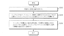
ここで、特に添付図を参照。当該添付図において、幾つかの図を通して類似の参照符号は、類似の部分/層を示す。図2は、実施具体例による被覆品の製造方法の実例を示すフローチャートである。ステップS202において、実質的に透明な基板を設ける。ある種の実施具体例において、実質的に透明な基板は、ガラス基板である。特に、ある種の実施具体例において、実質的に透明な基板は、ソーダ石灰フロートガラスであってもよい。もちろん、ある種の実施具体例に関連して、他の実質的に透明な基板を使用してもよい。実際、ある種の実施具体例において、還元鉄を含有するフロートガラス基板を使用する場合がある。 Here, particularly refer to the attached drawings. In the accompanying drawings, like reference numerals designate like parts / layers throughout the several views. FIG. 2 is a flowchart showing an example of a method for manufacturing a coated article according to an embodiment. In step S202, a substantially transparent substrate is provided. In certain example embodiments, the substantially transparent substrate is a glass substrate. In particular, in certain example embodiments, the substantially transparent substrate may be soda lime float glass. Of course, other substantially transparent substrates may be used in connection with certain example embodiments. Indeed, in certain example embodiments, a float glass substrate containing reduced iron may be used.
ステップS204において、インジウムスズ(InSn)ターゲットのスパッタリングによって、実質的に亜酸化のITOおよび/または金属モードのインジウムスズ膜をガラス基板上に蒸着する。ある種の実施具体例において、ターゲットのIn/Sn比は、約95/5から80/20まで、一層好ましくは90/10であってもよい。スパッタリングは、室温または室温近くで、例えば、約17〜25℃の温度、一層好ましくは約20℃で行われてもよい。蒸着過程を様々な環境下で行ってもよい。例えば、ある種の実施具体例において、実質的に純粋なAr環境下で蒸着過程を行う一方、ある種の実施具体例においては、酸素含有雰囲気(例えば、酸素およびアルゴンの混合物)中で蒸着過程を行う。後者の例において、酸素対アルゴン比は約0から1まで、一層好ましくは約0から0.4まで、さらに一層好ましくは約0から0.1まで変化してもよい。 In step S204, a substantially sub-oxidized ITO and / or metal mode indium tin film is deposited on the glass substrate by sputtering an indium tin (InSn) target. In certain example embodiments, the target In / Sn ratio may be from about 95/5 to 80/20, more preferably 90/10. Sputtering may be performed at or near room temperature, for example, at a temperature of about 17-25 ° C, more preferably at about 20 ° C. The deposition process may be performed in various environments. For example, in certain embodiments, the deposition process is performed in a substantially pure Ar environment, while in certain embodiments, the deposition process is performed in an oxygen-containing atmosphere (eg, a mixture of oxygen and argon). I do. In the latter example, the oxygen to argon ratio may vary from about 0 to 1, more preferably from about 0 to 0.4, and even more preferably from about 0 to 0.1.
室温または室温近くでスパッタリング蒸着するとき、実質的に亜酸化のITOまたは金属InSn膜は、可視光吸収がかなり高く、かつ高いシート抵抗を有する。しかしながら、以下に一層詳細に説明されるように、可視光吸収およびシート抵抗は、熱処理後に減少する場合がある。 When sputter deposited at or near room temperature, substantially sub-oxidized ITO or metal InSn films have significantly higher visible light absorption and higher sheet resistance. However, as will be explained in more detail below, visible light absorption and sheet resistance may decrease after heat treatment.
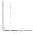
ターゲットの初期組成に依存して、蒸着材料(例えば、実質的に亜酸化のITOまたは金属InSn膜)は、アモルファス、InおよびSnの混合物、または様々な方向のITO微結晶を有してもよい。この点に関して、図3は、実施具体例による蒸着材料のX線回折(XRD)の幾つかの例を示すグラフである。図3のグラフは、蒸着材料の結晶方向を示す。(例えば、特定の角度で出力される光子または光線等を含む線の形状、ピーク間の幅等)の「特徴」に基づき、(a)はアモルファス結晶構造を示し、(b)はInおよびSnの混合物を示し、(c)および(d)は様々な方向のITO微結晶を示す。このように、スパッタリング後、x=1−y、かつyが約0から0.5まで、一層好ましくは0.1から0.3まで、およびさらに一層好ましくは約0.2で、一般に(InSn)xOyからなる材料を蒸着する。 Depending on the initial composition of the target, the deposition material (eg, substantially sub-oxidized ITO or metal InSn film) may have amorphous, a mixture of In and Sn, or ITO microcrystals in various directions. . In this regard, FIG. 3 is a graph showing some examples of X-ray diffraction (XRD) of vapor deposition materials according to an example embodiment. The graph of FIG. 3 shows the crystal direction of the vapor deposition material. (A) shows an amorphous crystal structure, (b) shows In and Sn based on “features” of (for example, the shape of a line including photons or light rays output at a specific angle, the width between peaks, etc.) (C) and (d) show ITO crystallites in various directions. Thus, after sputtering, x = 1−y and y is from about 0 to 0.5, more preferably from 0.1 to 0.3, and even more preferably about 0.2, generally (InSn ) depositing a material consisting x O y.
当然のことながら、ある種の実施具体例において、1以上の追加の層上に前記中間膜をスパッタリング蒸着してもよい。例えば、図示しない1以上のステップにおいて、例えば、誘電体のような緩衝膜上に中間膜をスパッタリング蒸着してもよい。当該誘電体は、中間膜およびガラス基板間に設けてもよい。このことは、実施具体例において利点がある場合がある。窒化ケイ素またはシリコンオキシ窒化物のような誘電体は、ガラスから諸元素(例えば、ソーダ石灰ガラスからアルカリ元素)の透明導電性酸化物(TCO)ITO層へのマイグレーション(migration)の低減に役立つからである。 Of course, in certain example embodiments, the intermediate film may be sputter deposited on one or more additional layers. For example, in one or more steps (not shown), for example, an intermediate film may be deposited by sputtering on a buffer film such as a dielectric. The dielectric may be provided between the intermediate film and the glass substrate. This may be advantageous in an embodiment. Dielectrics such as silicon nitride or silicon oxynitride can help reduce migration of elements from glass (eg, soda lime glass to alkali elements) to transparent conductive oxide (TCO) ITO layers. It is.
ステップS206において、スパッタリングによって被覆したガラス基板を熱処理して、実質的に亜酸化のITOおよび/または金属モードのインジウムスズ膜を、実質的に透明で導電性結晶ITO膜に変える。言い換えれば、熱処理過程は、すでに蒸着された膜の酸化を増大させる可能性がある。本明細書に記載された熱処理は、例えば、熱強化または熱による焼き戻しを含む。それゆえ、ある種の実施具体例において、蒸着された状態のインジウムスズまたはインジウムスズ酸化物膜を有するガラス基板を適切なサイズにカットし、その後600℃を上回る温度で熱的に強化し、続いて空気焼き入れをして、強化されたガラス基板上に導電性透明ITO膜を形成してもよい。熱的強化は、少なくとも約580℃、一層好ましくは少なくとも約600℃、しばしば少なくとも約620または640℃の温度で焼き戻し炉内において、上に蒸着された状態の膜を有するガラス基板の加熱を伴ってもよい。この発明のある種の実施具体例において、膜を上に有するガラス基板は、少なくとも約2分間、一層好ましくは、少なくとも約5分間焼き戻し炉内にあってもよい。 In step S206, the glass substrate coated by sputtering is heat-treated to convert the substantially sub-oxidized ITO and / or metal mode indium tin film into a substantially transparent and conductive crystalline ITO film. In other words, the heat treatment process can increase the oxidation of the already deposited film. The heat treatment described herein includes, for example, heat strengthening or heat tempering. Thus, in certain example embodiments, a glass substrate having a deposited indium tin or indium tin oxide film is cut to an appropriate size and then thermally strengthened at a temperature above 600 ° C., followed by The conductive transparent ITO film may be formed on the reinforced glass substrate by air quenching. Thermal strengthening involves heating a glass substrate having a film as deposited thereon in a tempering furnace at a temperature of at least about 580 ° C., more preferably at least about 600 ° C., often at least about 620 or 640 ° C. May be. In certain embodiments of the invention, the glass substrate having the film thereon may be in a tempering furnace for at least about 2 minutes, more preferably for at least about 5 minutes.
同様に、この発明のある種の実施具体例において、蒸着された状態のインジウムスズまたはインジウムスズ酸化物膜を有するガラス基板を600℃前後の温度で熱強化し、その後適当なサイズにカット(または、熱強化前に適当なサイズにカット)し、強化されたガラス基板上に導電性透明ITO膜を形成してもよい。 Similarly, in certain embodiments of the present invention, a glass substrate having an indium tin or indium tin oxide film as deposited is thermally strengthened at a temperature around 600 ° C. and then cut to an appropriate size (or The conductive transparent ITO film may be formed on a reinforced glass substrate by cutting into a suitable size before heat strengthening.
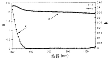
熱処理(例えば、熱による焼き戻しまたは熱強化)は、蒸着された状態の膜を現在作られているITOに似た光学定数を有する結晶透明導電性膜に変える。例えば、図4は、実施具体例による熱処理後に蒸着された材料のX線回折(XRD)を示すグラフである。図4のグラフは、一般にTCO、特にITO特有の結晶構造に似ている。さらに、図5は、実施具体例による熱処理後の蒸着材料の光学定数を示すグラフである。図5の例において、屈折率(n)は、実質的に可視スペクトル(例えば、約400〜700nm波長)の全てにわたって、そして近赤外(NIR)スペクトル(約700〜1100nm波長)においても約2である。一方、吸光係数(k)は高いが、可視スペクトルの実質的全てにわたって、そしてNIRスペクトルにおいても0に近い値に急落する。言い換えれば、ITO材料の減衰すなわち吸収効果は、熱処理後極めて低い。 A heat treatment (eg, tempering by heat or heat strengthening) changes the deposited film to a crystalline transparent conductive film having an optical constant similar to that of ITO currently made. For example, FIG. 4 is a graph showing X-ray diffraction (XRD) of a material deposited after heat treatment according to an example embodiment. The graph of FIG. 4 generally resembles the crystal structure typical of TCO, especially ITO. Further, FIG. 5 is a graph showing optical constants of the vapor deposition material after the heat treatment according to the embodiment. In the example of FIG. 5, the refractive index (n) is approximately 2 over the entire visible spectrum (eg, about 400-700 nm wavelength) and also in the near infrared (NIR) spectrum (about 700-1100 nm wavelength). It is. On the other hand, although the extinction coefficient (k) is high, it suddenly drops to a value close to 0 over substantially the entire visible spectrum and also in the NIR spectrum. In other words, the attenuation or absorption effect of the ITO material is very low after heat treatment.
実際、ある種の実施形態において、ITOの屈折率(n)は、好ましくは約1.8〜2.2である。一方、ITOの吸光係数(k)は、好ましくは約0.5より低く、一層好ましくは約0.3より低く、一層好ましくは0.2より低い。上述の通り、ITO被膜のシート抵抗および可視透過率が低減される。すなわち、ある種の実施形態において、シート抵抗は、約70オーム/sq.より低く、一層好ましくは約50オーム/sq.より低い。一方、ITO(および/またはITOに関連して設けられる追加の層)の可視透過率は、少なくとも約70%、一層好ましくは少なくとも約75%、さらに一層好ましくは少なくとも約80%である。 Indeed, in certain embodiments, the refractive index (n) of ITO is preferably about 1.8 to 2.2. On the other hand, the extinction coefficient (k) of ITO is preferably less than about 0.5, more preferably less than about 0.3, and more preferably less than 0.2. As described above, the sheet resistance and visible transmittance of the ITO coating are reduced. That is, in certain embodiments, the sheet resistance is about 70 ohms / sq. Lower, more preferably about 50 ohm / sq. Lower. On the other hand, the visible transmission of ITO (and / or additional layers provided in connection with ITO) is at least about 70%, more preferably at least about 75%, and even more preferably at least about 80%.
層、膜、または材料は、別の層、膜、または材料「上にある」または「によって支持される」ものと考えられるが、当然のことながら、追加の層、膜、および/または材料をそれらの間に設けてもよい。言い換えれば、層、膜、または材料は、直接互いに隣接していない別の層、膜、または材料「上にある」または「によって支持される」ものと考えてもよい。 A layer, membrane, or material is considered to be “on” or “supported by” another layer, membrane, or material, but it should be understood that additional layers, membranes, and / or materials You may provide between them. In other words, a layer, membrane or material may be considered to be “on” or “supported” by another layer, membrane or material that is not directly adjacent to each other.
さらに、ある種の実施具体例は、タッチパネルディスプレイに関するものと記載されているが、当然のことながら、本明細書に記載されている技術を他の用途に適用してもよい。例えば、実質的に亜酸化のインジウムスズ酸化物(ITO)および/または金属モードのインジウムスズ膜からなる中間膜を、直接的または間接的に基板上に蒸着し、合成ITOからなる膜を作る技術を幅広い種類の用途に関連して使用してもよい。 Furthermore, although certain example embodiments are described as relating to touch panel displays, it will be appreciated that the techniques described herein may be applied to other applications. For example, a technique for forming a film made of synthetic ITO by directly or indirectly depositing an intermediate film made of suboxide indium tin oxide (ITO) and / or a metal mode indium tin film on a substrate. May be used in connection with a wide variety of applications.
この発明のある種の実施具体例において、図面の様々な層用に示される材料は、好ましい材料である一方、明示的に主張しないかぎりは、限定を目的とするものではない。この発明の他の実施具体例において、他の材料を図面に示される材料を置換するために使用してもよい。さらに、この発明の他の実施具体例において一部の層を除去してもよいし、他の層を追加してもよい。同様に、例示された厚みもまた、明示的に主張しないかぎりは、限定を目的とするものではない。 In certain embodiments of the invention, the materials shown for the various layers of the drawings are preferred materials, but are not intended to be limiting unless explicitly stated. In other embodiments of the present invention, other materials may be used to replace the materials shown in the drawings. Furthermore, in other embodiments of the present invention, some layers may be removed or other layers may be added. Similarly, the exemplified thicknesses are also not intended to be limiting unless explicitly stated.
この発明は、最も実用的かつ好ましい実施具体例と現在考えられているものに関連して記載される一方で、この発明が開示された実施具体例に限定されないことを理解すべきである。それどころか、この発明は、添付の特許請求の範囲の精神および当該範囲内に含まれる様々な改良および同等の装置を保護することを目的としている。 While this invention has been described in connection with what is presently considered to be the most practical and preferred embodiment, it is to be understood that this invention is not limited to the disclosed embodiment. On the contrary, the invention is intended to protect the spirit of the appended claims and various modifications and equivalent devices falling within the scope of the appended claims.
Claims (21)
インジウムスズ(InSn)をターゲットとするスパッタリングによって、実質的に亜酸化のインジウムスズ酸化物(ITO)および/または金属モードのインジウムスズ膜で直接的または間接的に基板を覆い、
前記スパッタリングは、室温または室温に近い温度で行われ、
実質的に亜酸化のITOおよび/または金属モードのインジウムスズ膜を有する前記基板を熱処理して、実質的に亜酸化のITOおよび/または金属モードのインジウムスズ膜の層を実質的に透明で導電性を有する結晶性の合成ITO膜に変換する工程を備えた被覆品の製造方法。 Providing a substantially transparent substrate,
Sputtering targeting indium tin (InSn) directly or indirectly covering the substrate with substantially sub-oxide indium tin oxide (ITO) and / or metal mode indium tin film,
The sputtering is performed at or near room temperature,
The substrate having a substantially sub-oxidized ITO and / or metal mode indium tin film is heat treated so that the substantially sub-oxidized ITO and / or metal mode indium tin film layer is substantially transparent and conductive. For producing a coated product comprising a step of converting into a crystalline synthetic ITO film having a property.
インジウムスズ(InSn)をターゲットとするスパッタリングによって、中間膜で直接的または間接的に基板を覆い、
前記中間膜は、実質的に亜酸化のインジウムスズ酸化物(ITO)および/または金属モードのインジウムスズ膜からなり、
前記スパッタリングは、室温または室温に近い温度で行われ、
前記中間膜とともに基板を熱強化するか、または熱による焼き戻しを行って導電性を有する結晶性の合成ITO膜を作り、
前記中間膜は、(InSn)xOyからなり、0<y<0.5、かつx=1−yであり、
前記スパッタリングを0から0.4まで、一層好ましくは0から0.1までの酸素対アルゴン比を有する環境で行う工程を備えた被覆品の製造方法。 Providing a substantially transparent soda-lime float glass substrate,
Covering the substrate directly or indirectly with an intermediate film by sputtering with indium tin (InSn) as a target,
The intermediate film is substantially composed of sub-oxide indium tin oxide (ITO) and / or metal mode indium tin film,
The sputtering is performed at or near room temperature,
The substrate is thermally strengthened together with the intermediate film, or heat tempering is performed to make a crystalline synthetic ITO film having conductivity,
The intermediate film is made of (InSn) x O y , 0 <y <0.5, and x = 1−y,
A method for producing a coated article comprising the step of performing said sputtering in an environment having an oxygen to argon ratio of 0 to 0.4, more preferably 0 to 0.1.
ITO被膜からなる被覆品を設け、
被覆品は、インジウムスズ(InSn)をターゲットとするスパッタリングによって直接的または間接的に基板を覆う中間膜を有し、
前記中間膜は、実質的に亜酸化のインジウムスズ酸化物(ITO)および/または金属モードのインジウムスズ膜からなり、
前記スパッタリングは、室温または室温に近い温度で行われ、
基板および中間膜を熱処理して導電性を有する結晶性の合成ITO膜を作り、
前記中間膜は、(InSn)xOyからなり、0<y<0.5、かつx=1−yであり、
前記スパッタリングを0から0.4まで、一層好ましくは0から0.1までの酸素対アルゴン比を有する環境で行う工程を備えたタッチパネルディスプレイ装置の製造方法。 A display panel,
A coated product made of an ITO film is provided,
The coated product has an intermediate film that directly or indirectly covers the substrate by sputtering using indium tin (InSn) as a target;
The intermediate film is substantially composed of sub-oxide indium tin oxide (ITO) and / or metal mode indium tin film,
The sputtering is performed at or near room temperature,
Heat-treat the substrate and the intermediate film to make a crystalline synthetic ITO film having conductivity,
The intermediate film is made of (InSn) x O y , 0 <y <0.5, and x = 1−y,
A method of manufacturing a touch panel display device comprising a step of performing the sputtering in an environment having an oxygen to argon ratio of 0 to 0.4, more preferably 0 to 0.1.
Applications Claiming Priority (3)
| Application Number | Priority Date | Filing Date | Title |
|---|---|---|---|
| US12/292,406 | 2008-11-18 | ||
| US12/292,406 US8080141B2 (en) | 2008-11-18 | 2008-11-18 | ITO-coated article and/or method of making the same via heat treating |
| PCT/US2009/060416 WO2010059311A1 (en) | 2008-11-18 | 2009-10-13 | Ito-coated article for use with touch panel display assemblies, and/or method of making the same |
Publications (1)
| Publication Number | Publication Date |
|---|---|
| JP2012509397A true JP2012509397A (en) | 2012-04-19 |
Family
ID=41478945
Family Applications (1)
| Application Number | Title | Priority Date | Filing Date |
|---|---|---|---|
| JP2011536361A Pending JP2012509397A (en) | 2008-11-18 | 2009-10-13 | Method for manufacturing ITO coated product for use with touch panel display and / or method for manufacturing said ITO coated product |
Country Status (7)
| Country | Link |
|---|---|
| US (3) | US8080141B2 (en) |
| EP (1) | EP2370611A1 (en) |
| JP (1) | JP2012509397A (en) |
| KR (1) | KR20110098706A (en) |
| BR (1) | BRPI0921775A2 (en) |
| TW (1) | TW201022458A (en) |
| WO (1) | WO2010059311A1 (en) |
Cited By (1)
| Publication number | Priority date | Publication date | Assignee | Title |
|---|---|---|---|---|
| JP2015074788A (en) * | 2013-10-07 | 2015-04-20 | 三菱マテリアル株式会社 | In SPUTTERING TARGET AND In FILM |
Families Citing this family (30)
| Publication number | Priority date | Publication date | Assignee | Title |
|---|---|---|---|---|
| US8080141B2 (en) | 2008-11-18 | 2011-12-20 | Guardian Industries Corp. | ITO-coated article and/or method of making the same via heat treating |
| US8236118B2 (en) | 2009-08-07 | 2012-08-07 | Guardian Industries Corp. | Debonding and transfer techniques for hetero-epitaxially grown graphene, and products including the same |
| RU2558063C2 (en) | 2010-01-16 | 2015-07-27 | КАРДИНАЛ СиДжи КОМПАНИ | High-quality low-emission coatings, low-emission insulated glazing and methods for production thereof |
| US10000411B2 (en) | 2010-01-16 | 2018-06-19 | Cardinal Cg Company | Insulating glass unit transparent conductivity and low emissivity coating technology |
| US10060180B2 (en) | 2010-01-16 | 2018-08-28 | Cardinal Cg Company | Flash-treated indium tin oxide coatings, production methods, and insulating glass unit transparent conductive coating technology |
| US10000965B2 (en) | 2010-01-16 | 2018-06-19 | Cardinal Cg Company | Insulating glass unit transparent conductive coating technology |
| KR101298837B1 (en) * | 2010-06-25 | 2013-08-23 | 주식회사 유아이디 | Method of manufacturing an ito coating glass for a touch panel and sputtering apparatus used in the same |
| KR101167418B1 (en) * | 2010-09-20 | 2012-07-19 | 삼성전기주식회사 | Touch Screen |
| US20130019934A1 (en) * | 2011-07-22 | 2013-01-24 | Primestar Solar, Inc. | Oxygen getter layer for photovoltaic devices and methods of their manufacture |
| CN104145239A (en) * | 2012-02-24 | 2014-11-12 | 松下电器产业株式会社 | input device |
| US8766245B2 (en) | 2012-08-14 | 2014-07-01 | Guardian Industries Corp. | Organic light emitting diode with transparent electrode and method of making same |
| US8524526B1 (en) * | 2012-08-14 | 2013-09-03 | Guardian Industries Corp. | Organic light emitting diode with transparent electrode and method of making same |
| US9733779B2 (en) | 2012-11-27 | 2017-08-15 | Guardian Industries Corp. | Projected capacitive touch panel with silver-inclusive transparent conducting layer(s), and/or method of making the same |
| US9354755B2 (en) | 2012-11-27 | 2016-05-31 | Guardian Industries Corp. | Projected capacitive touch panel with a silver-inclusive transparent conducting layer(s) |
| US10216347B2 (en) | 2012-11-27 | 2019-02-26 | Guardian Glass, LLC | Transparent conductive coating for capacitive touch panel with silver having adjusted resistance |
| US9557871B2 (en) | 2015-04-08 | 2017-01-31 | Guardian Industries Corp. | Transparent conductive coating for capacitive touch panel or the like |
| US10222921B2 (en) | 2012-11-27 | 2019-03-05 | Guardian Glass, LLC | Transparent conductive coating for capacitive touch panel with silver having increased resistivity |
| US10248274B2 (en) | 2012-11-27 | 2019-04-02 | Guardian Glass, LLC | Transparent conductive coating for capacitive touch panel and method of making same |
| JP5672338B2 (en) * | 2013-06-04 | 2015-02-18 | Smk株式会社 | Touch panel and method for manufacturing touch panel |
| US9988707B2 (en) | 2014-05-30 | 2018-06-05 | Ppg Industries Ohio, Inc. | Transparent conducting indium doped tin oxide |
| US10133108B2 (en) | 2015-04-08 | 2018-11-20 | Guardian Glass, LLC | Vending machines with large area transparent touch electrode technology, and/or associated methods |
| US10145005B2 (en) | 2015-08-19 | 2018-12-04 | Guardian Glass, LLC | Techniques for low temperature direct graphene growth on glass |
| KR102513362B1 (en) | 2015-12-11 | 2023-03-24 | 삼성디스플레이 주식회사 | Liquid crystal display panel and method of manufacturing the same |
| KR102159491B1 (en) | 2016-05-09 | 2020-09-24 | 주식회사 엘지화학 | A conductive transparent film |
| WO2017196034A1 (en) * | 2016-05-09 | 2017-11-16 | 주식회사 엘지화학 | Conductive light-transmissive film |
| KR20190085487A (en) * | 2018-01-10 | 2019-07-18 | 어플라이드 머티어리얼스, 인코포레이티드 | Pvd films for euv lithography |
| US10539864B2 (en) | 2018-02-08 | 2020-01-21 | Guardian Glass, LLC | Capacitive touch panel having diffuser and patterned electrode |
| US11028012B2 (en) | 2018-10-31 | 2021-06-08 | Cardinal Cg Company | Low solar heat gain coatings, laminated glass assemblies, and methods of producing same |
| FR3088850B1 (en) * | 2018-11-28 | 2020-12-11 | Saint Gobain | PROCESS FOR MANUFACTURING AN ELECTROCHROME WINDOW |
| CN114436538B (en) * | 2021-12-20 | 2023-05-30 | 凯盛信息显示材料(洛阳)有限公司 | High-transmittance shadow-eliminating conductive glass and manufacturing method thereof |
Citations (5)
| Publication number | Priority date | Publication date | Assignee | Title |
|---|---|---|---|---|
| JPS59116138A (en) * | 1982-11-03 | 1984-07-04 | ドネリ−・ミラ−ズ・インコ−ポレイテツド | Manufacture of bended electroconductively coated glass member and products |
| JPS6212010A (en) * | 1985-07-09 | 1987-01-21 | 富士通株式会社 | Method for forming a transparent conductor film |
| JPH09226046A (en) * | 1996-02-22 | 1997-09-02 | Mitsui Toatsu Chem Inc | Transparent conductive laminate and method for producing the same |
| JP2004149400A (en) * | 2002-09-02 | 2004-05-27 | Asahi Glass Co Ltd | Insulated glass and method for producing the same |
| JP2007311040A (en) * | 2006-05-16 | 2007-11-29 | Bridgestone Corp | Method for forming crystalline ITO thin film, crystalline ITO thin film and film, and resistive touch panel |
Family Cites Families (19)
| Publication number | Priority date | Publication date | Assignee | Title |
|---|---|---|---|---|
| FR2633920B1 (en) * | 1988-07-08 | 1992-02-21 | Saint Gobain Vitrage | PROCESS FOR PRODUCING A LOW RESISTIVITY TRANSPARENT LAYER |
| US5650597A (en) | 1995-01-20 | 1997-07-22 | Dynapro Systems, Inc. | Capacitive touch sensor |
| US6123415A (en) * | 1995-12-21 | 2000-09-26 | Kabushiki Kaisha Toshiba | Ink jet recording apparatus |
| AU715152B2 (en) * | 1996-01-26 | 2000-01-20 | Tetra Laval Holdings & Finance Sa | Method and apparatus for printing images on packaging material |
| GB9626696D0 (en) * | 1996-12-23 | 1997-02-12 | Ishida Seisakusho | Method of printing film at form-fill-seal packaging machine form-fill-seal packaging machine using the method |
| US6204897B1 (en) | 1998-08-18 | 2001-03-20 | International Business Machines Corporation | Integrated resistor for measuring touch position in a liquid crystal display device |
| US6057903A (en) | 1998-08-18 | 2000-05-02 | International Business Machines Corporation | Liquid crystal display device employing a guard plane between a layer for measuring touch position and common electrode layer |
| DE19913855A1 (en) * | 1999-03-26 | 2000-09-28 | Focke & Co | Method and device for printing blanks |
| JP2001315321A (en) * | 2000-05-11 | 2001-11-13 | Fuji Photo Film Co Ltd | Ink jet printing method and printer |
| DE60122077T2 (en) | 2000-09-14 | 2007-02-15 | Asahi Glass Co., Ltd. | Laminated glass |
| US6743488B2 (en) * | 2001-05-09 | 2004-06-01 | Cpfilms Inc. | Transparent conductive stratiform coating of indium tin oxide |
| DE10228523B4 (en) | 2001-11-14 | 2017-09-21 | Lg Display Co., Ltd. | touch tablet |
| US6550905B1 (en) * | 2001-11-19 | 2003-04-22 | Dotrix N.V. | Radiation curable inkjet ink relatively free of photoinitiator and method and apparatus of curing the ink |
| US7372510B2 (en) | 2002-03-01 | 2008-05-13 | Planar Systems, Inc. | Reflection resistant touch screens |
| KR100480823B1 (en) | 2002-11-14 | 2005-04-07 | 엘지.필립스 엘시디 주식회사 | touch panel for display device |
| WO2006061964A1 (en) * | 2004-12-08 | 2006-06-15 | Asahi Glass Company, Limited | Substratum with conductive film and process for producing the same |
| JPWO2007029457A1 (en) | 2005-09-02 | 2009-03-12 | 出光興産株式会社 | Conductive composition film, electron injection electrode, and organic electroluminescence device |
| TWI325639B (en) * | 2007-03-15 | 2010-06-01 | Au Optronics Corp | Semiconductor structure and fabricating method thereof for liquid crystal display device |
| US8080141B2 (en) | 2008-11-18 | 2011-12-20 | Guardian Industries Corp. | ITO-coated article and/or method of making the same via heat treating |
-
2008
- 2008-11-18 US US12/292,406 patent/US8080141B2/en not_active Expired - Fee Related
-
2009
- 2009-10-13 WO PCT/US2009/060416 patent/WO2010059311A1/en active Application Filing
- 2009-10-13 KR KR1020117003074A patent/KR20110098706A/en not_active Withdrawn
- 2009-10-13 EP EP09740586A patent/EP2370611A1/en not_active Withdrawn
- 2009-10-13 JP JP2011536361A patent/JP2012509397A/en active Pending
- 2009-10-13 BR BRPI0921775A patent/BRPI0921775A2/en not_active IP Right Cessation
- 2009-10-22 TW TW098135765A patent/TW201022458A/en unknown
-
2011
- 2011-11-22 US US13/302,052 patent/US8313620B2/en not_active Expired - Fee Related
-
2012
- 2012-11-05 US US13/668,732 patent/US8518221B2/en not_active Expired - Fee Related
Patent Citations (5)
| Publication number | Priority date | Publication date | Assignee | Title |
|---|---|---|---|---|
| JPS59116138A (en) * | 1982-11-03 | 1984-07-04 | ドネリ−・ミラ−ズ・インコ−ポレイテツド | Manufacture of bended electroconductively coated glass member and products |
| JPS6212010A (en) * | 1985-07-09 | 1987-01-21 | 富士通株式会社 | Method for forming a transparent conductor film |
| JPH09226046A (en) * | 1996-02-22 | 1997-09-02 | Mitsui Toatsu Chem Inc | Transparent conductive laminate and method for producing the same |
| JP2004149400A (en) * | 2002-09-02 | 2004-05-27 | Asahi Glass Co Ltd | Insulated glass and method for producing the same |
| JP2007311040A (en) * | 2006-05-16 | 2007-11-29 | Bridgestone Corp | Method for forming crystalline ITO thin film, crystalline ITO thin film and film, and resistive touch panel |
Non-Patent Citations (1)
| Title |
|---|
| JPN5012003483; CHAUDHURI S: 'MICROSTRUCTURE OF INDIUM TIN OXIDE FILMS PRODUCED BY THE D.C. SPUTTERING TECHNIQUE' THIN SOLID FILMS V148 N3, 19870427, P279-284, ELSEVIER-SEQUOIA S.A. * |
Cited By (1)
| Publication number | Priority date | Publication date | Assignee | Title |
|---|---|---|---|---|
| JP2015074788A (en) * | 2013-10-07 | 2015-04-20 | 三菱マテリアル株式会社 | In SPUTTERING TARGET AND In FILM |
Also Published As
| Publication number | Publication date |
|---|---|
| US20120064234A1 (en) | 2012-03-15 |
| US20100122900A1 (en) | 2010-05-20 |
| EP2370611A1 (en) | 2011-10-05 |
| TW201022458A (en) | 2010-06-16 |
| WO2010059311A1 (en) | 2010-05-27 |
| US8313620B2 (en) | 2012-11-20 |
| US20130059065A1 (en) | 2013-03-07 |
| KR20110098706A (en) | 2011-09-01 |
| US8080141B2 (en) | 2011-12-20 |
| BRPI0921775A2 (en) | 2016-01-12 |
| US8518221B2 (en) | 2013-08-27 |
Similar Documents
| Publication | Publication Date | Title |
|---|---|---|
| JP2012509397A (en) | Method for manufacturing ITO coated product for use with touch panel display and / or method for manufacturing said ITO coated product | |
| US8298380B2 (en) | Method of making thermally tempered coated article with transparent conductive oxide (TCO) coating in color compression configuration, and product made using same | |
| JP6328122B2 (en) | Low emissivity coated products with low visible light transmission | |
| US7597964B2 (en) | Thermally tempered coated article with transparent conductive oxide (TCO) coating | |
| JPH02217339A (en) | transparent conductive glass | |
| KR20170077217A (en) | Anti-reflective coated glass article | |
| CN103561951A (en) | Low emissivity laminate and multi-layer glass | |
| EP2148240B1 (en) | Transparent electrode | |
| CN102194539A (en) | Transparent conductive laminate and method for producing same | |
| TW201422836A (en) | Method for producing substrate with transparent electrode, and substrate with transparent electrode | |
| JPH08111123A (en) | Transparent conductive film, method for producing the same, and sputtering target | |
| KR101768286B1 (en) | Conductive structure body precursor, conductive structure body and method for manufacturing the same | |
| KR102791294B1 (en) | Transparent conductive film | |
| JP2001210144A (en) | Substrate with transparent conductive film and method of manufacturing the same | |
| TWI322277B (en) | ||
| JP2005190700A (en) | Substrate with transparent conductive film and method for producing the same | |
| JP3630374B2 (en) | Glass with transparent conductive film and method for forming transparent conductive film | |
| WO2021024944A1 (en) | Transparent conductive film | |
| WO2021001691A4 (en) | Transparent conductive film | |
| CN116940537A (en) | Transparent substrate with multilayer film and image display device | |
| JPH07291664A (en) | Transparent conductive thin film | |
| JPH06320661A (en) | Production of transparent conductive film |
Legal Events
| Date | Code | Title | Description |
|---|---|---|---|
| A621 | Written request for application examination |
Free format text: JAPANESE INTERMEDIATE CODE: A621 Effective date: 20120919 |
|
| A977 | Report on retrieval |
Free format text: JAPANESE INTERMEDIATE CODE: A971007 Effective date: 20131010 |
|
| A131 | Notification of reasons for refusal |
Free format text: JAPANESE INTERMEDIATE CODE: A131 Effective date: 20131022 |
|
| A601 | Written request for extension of time |
Free format text: JAPANESE INTERMEDIATE CODE: A601 Effective date: 20140116 |
|
| A602 | Written permission of extension of time |
Free format text: JAPANESE INTERMEDIATE CODE: A602 Effective date: 20140123 |
|
| A02 | Decision of refusal |
Free format text: JAPANESE INTERMEDIATE CODE: A02 Effective date: 20150106 |