JP2012256919A - Manufacturing method for semiconductor package - Google Patents
Manufacturing method for semiconductor package Download PDFInfo
- Publication number
- JP2012256919A JP2012256919A JP2012174235A JP2012174235A JP2012256919A JP 2012256919 A JP2012256919 A JP 2012256919A JP 2012174235 A JP2012174235 A JP 2012174235A JP 2012174235 A JP2012174235 A JP 2012174235A JP 2012256919 A JP2012256919 A JP 2012256919A
- Authority
- JP
- Japan
- Prior art keywords
- semiconductor package
- electrode pattern
- circuit board
- semiconductor chip
- manufacturing
- Prior art date
- Legal status (The legal status is an assumption and is not a legal conclusion. Google has not performed a legal analysis and makes no representation as to the accuracy of the status listed.)
- Pending
Links
- 239000004065 semiconductor Substances 0.000 title claims abstract description 98
- 238000004519 manufacturing process Methods 0.000 title claims abstract description 32
- 238000000034 method Methods 0.000 claims description 34
- 238000007747 plating Methods 0.000 claims description 14
- 239000010949 copper Substances 0.000 claims description 8
- 230000004308 accommodation Effects 0.000 claims description 7
- 239000000758 substrate Substances 0.000 claims description 7
- RYGMFSIKBFXOCR-UHFFFAOYSA-N Copper Chemical compound [Cu] RYGMFSIKBFXOCR-UHFFFAOYSA-N 0.000 claims description 5
- 229910052802 copper Inorganic materials 0.000 claims description 5
- 230000001681 protective effect Effects 0.000 claims description 4
- 238000004544 sputter deposition Methods 0.000 claims description 4
- 239000004020 conductor Substances 0.000 claims description 2
- 229920002120 photoresistant polymer Polymers 0.000 description 8
- 230000000694 effects Effects 0.000 description 4
- 230000008901 benefit Effects 0.000 description 3
- 239000000463 material Substances 0.000 description 3
- CURLTUGMZLYLDI-UHFFFAOYSA-N Carbon dioxide Chemical compound O=C=O CURLTUGMZLYLDI-UHFFFAOYSA-N 0.000 description 2
- 238000009713 electroplating Methods 0.000 description 2
- 238000005516 engineering process Methods 0.000 description 2
- 239000004593 Epoxy Substances 0.000 description 1
- 239000004642 Polyimide Substances 0.000 description 1
- 229910052581 Si3N4 Inorganic materials 0.000 description 1
- VYPSYNLAJGMNEJ-UHFFFAOYSA-N Silicium dioxide Chemical compound O=[Si]=O VYPSYNLAJGMNEJ-UHFFFAOYSA-N 0.000 description 1
- XUIMIQQOPSSXEZ-UHFFFAOYSA-N Silicon Chemical compound [Si] XUIMIQQOPSSXEZ-UHFFFAOYSA-N 0.000 description 1
- UMIVXZPTRXBADB-UHFFFAOYSA-N benzocyclobutene Chemical compound C1=CC=C2CCC2=C1 UMIVXZPTRXBADB-UHFFFAOYSA-N 0.000 description 1
- 229910002092 carbon dioxide Inorganic materials 0.000 description 1
- 239000001569 carbon dioxide Substances 0.000 description 1
- 239000000470 constituent Substances 0.000 description 1
- 238000005553 drilling Methods 0.000 description 1
- 238000001312 dry etching Methods 0.000 description 1
- 238000005530 etching Methods 0.000 description 1
- 239000011810 insulating material Substances 0.000 description 1
- 239000002184 metal Substances 0.000 description 1
- 229910052751 metal Inorganic materials 0.000 description 1
- 229920002577 polybenzoxazole Polymers 0.000 description 1
- 229920001721 polyimide Polymers 0.000 description 1
- 229910052710 silicon Inorganic materials 0.000 description 1
- 239000010703 silicon Substances 0.000 description 1
- HQVNEWCFYHHQES-UHFFFAOYSA-N silicon nitride Chemical compound N12[Si]34N5[Si]62N3[Si]51N64 HQVNEWCFYHHQES-UHFFFAOYSA-N 0.000 description 1
- 229910052814 silicon oxide Inorganic materials 0.000 description 1
- 238000001039 wet etching Methods 0.000 description 1
Images


Classifications
-
- H—ELECTRICITY
- H01—ELECTRIC ELEMENTS
- H01L—SEMICONDUCTOR DEVICES NOT COVERED BY CLASS H10
- H01L23/00—Details of semiconductor or other solid state devices
- H01L23/52—Arrangements for conducting electric current within the device in operation from one component to another, i.e. interconnections, e.g. wires, lead frames
- H01L23/538—Arrangements for conducting electric current within the device in operation from one component to another, i.e. interconnections, e.g. wires, lead frames the interconnection structure between a plurality of semiconductor chips being formed on, or in, insulating substrates
- H01L23/5389—Arrangements for conducting electric current within the device in operation from one component to another, i.e. interconnections, e.g. wires, lead frames the interconnection structure between a plurality of semiconductor chips being formed on, or in, insulating substrates the chips being integrally enclosed by the interconnect and support structures
-
- H—ELECTRICITY
- H01—ELECTRIC ELEMENTS
- H01L—SEMICONDUCTOR DEVICES NOT COVERED BY CLASS H10
- H01L23/00—Details of semiconductor or other solid state devices
- H01L23/48—Arrangements for conducting electric current to or from the solid state body in operation, e.g. leads, terminal arrangements ; Selection of materials therefor
-
- H—ELECTRICITY
- H01—ELECTRIC ELEMENTS
- H01L—SEMICONDUCTOR DEVICES NOT COVERED BY CLASS H10
- H01L24/00—Arrangements for connecting or disconnecting semiconductor or solid-state bodies; Methods or apparatus related thereto
- H01L24/01—Means for bonding being attached to, or being formed on, the surface to be connected, e.g. chip-to-package, die-attach, "first-level" interconnects; Manufacturing methods related thereto
- H01L24/18—High density interconnect [HDI] connectors; Manufacturing methods related thereto
- H01L24/23—Structure, shape, material or disposition of the high density interconnect connectors after the connecting process
- H01L24/24—Structure, shape, material or disposition of the high density interconnect connectors after the connecting process of an individual high density interconnect connector
-
- H—ELECTRICITY
- H01—ELECTRIC ELEMENTS
- H01L—SEMICONDUCTOR DEVICES NOT COVERED BY CLASS H10
- H01L24/00—Arrangements for connecting or disconnecting semiconductor or solid-state bodies; Methods or apparatus related thereto
- H01L24/80—Methods for connecting semiconductor or other solid state bodies using means for bonding being attached to, or being formed on, the surface to be connected
- H01L24/82—Methods for connecting semiconductor or other solid state bodies using means for bonding being attached to, or being formed on, the surface to be connected by forming build-up interconnects at chip-level, e.g. for high density interconnects [HDI]
-
- H—ELECTRICITY
- H01—ELECTRIC ELEMENTS
- H01L—SEMICONDUCTOR DEVICES NOT COVERED BY CLASS H10
- H01L2224/00—Indexing scheme for arrangements for connecting or disconnecting semiconductor or solid-state bodies and methods related thereto as covered by H01L24/00
- H01L2224/01—Means for bonding being attached to, or being formed on, the surface to be connected, e.g. chip-to-package, die-attach, "first-level" interconnects; Manufacturing methods related thereto
- H01L2224/02—Bonding areas; Manufacturing methods related thereto
- H01L2224/023—Redistribution layers [RDL] for bonding areas
- H01L2224/0231—Manufacturing methods of the redistribution layers
-
- H—ELECTRICITY
- H01—ELECTRIC ELEMENTS
- H01L—SEMICONDUCTOR DEVICES NOT COVERED BY CLASS H10
- H01L2224/00—Indexing scheme for arrangements for connecting or disconnecting semiconductor or solid-state bodies and methods related thereto as covered by H01L24/00
- H01L2224/01—Means for bonding being attached to, or being formed on, the surface to be connected, e.g. chip-to-package, die-attach, "first-level" interconnects; Manufacturing methods related thereto
- H01L2224/18—High density interconnect [HDI] connectors; Manufacturing methods related thereto
- H01L2224/23—Structure, shape, material or disposition of the high density interconnect connectors after the connecting process
- H01L2224/24—Structure, shape, material or disposition of the high density interconnect connectors after the connecting process of an individual high density interconnect connector
- H01L2224/241—Disposition
- H01L2224/24151—Connecting between a semiconductor or solid-state body and an item not being a semiconductor or solid-state body, e.g. chip-to-substrate, chip-to-passive
- H01L2224/24221—Connecting between a semiconductor or solid-state body and an item not being a semiconductor or solid-state body, e.g. chip-to-substrate, chip-to-passive the body and the item being stacked
- H01L2224/24225—Connecting between a semiconductor or solid-state body and an item not being a semiconductor or solid-state body, e.g. chip-to-substrate, chip-to-passive the body and the item being stacked the item being non-metallic, e.g. insulating substrate with or without metallisation
- H01L2224/24226—Connecting between a semiconductor or solid-state body and an item not being a semiconductor or solid-state body, e.g. chip-to-substrate, chip-to-passive the body and the item being stacked the item being non-metallic, e.g. insulating substrate with or without metallisation the HDI interconnect connecting to the same level of the item at which the semiconductor or solid-state body is mounted, e.g. the item being planar
-
- H—ELECTRICITY
- H01—ELECTRIC ELEMENTS
- H01L—SEMICONDUCTOR DEVICES NOT COVERED BY CLASS H10
- H01L23/00—Details of semiconductor or other solid state devices
- H01L23/48—Arrangements for conducting electric current to or from the solid state body in operation, e.g. leads, terminal arrangements ; Selection of materials therefor
- H01L23/488—Arrangements for conducting electric current to or from the solid state body in operation, e.g. leads, terminal arrangements ; Selection of materials therefor consisting of soldered or bonded constructions
- H01L23/498—Leads, i.e. metallisations or lead-frames on insulating substrates, e.g. chip carriers
- H01L23/49827—Via connections through the substrates, e.g. pins going through the substrate, coaxial cables
-
- H—ELECTRICITY
- H01—ELECTRIC ELEMENTS
- H01L—SEMICONDUCTOR DEVICES NOT COVERED BY CLASS H10
- H01L2924/00—Indexing scheme for arrangements or methods for connecting or disconnecting semiconductor or solid-state bodies as covered by H01L24/00
- H01L2924/01—Chemical elements
- H01L2924/01005—Boron [B]
-
- H—ELECTRICITY
- H01—ELECTRIC ELEMENTS
- H01L—SEMICONDUCTOR DEVICES NOT COVERED BY CLASS H10
- H01L2924/00—Indexing scheme for arrangements or methods for connecting or disconnecting semiconductor or solid-state bodies as covered by H01L24/00
- H01L2924/01—Chemical elements
- H01L2924/01006—Carbon [C]
-
- H—ELECTRICITY
- H01—ELECTRIC ELEMENTS
- H01L—SEMICONDUCTOR DEVICES NOT COVERED BY CLASS H10
- H01L2924/00—Indexing scheme for arrangements or methods for connecting or disconnecting semiconductor or solid-state bodies as covered by H01L24/00
- H01L2924/01—Chemical elements
- H01L2924/01029—Copper [Cu]
-
- H—ELECTRICITY
- H01—ELECTRIC ELEMENTS
- H01L—SEMICONDUCTOR DEVICES NOT COVERED BY CLASS H10
- H01L2924/00—Indexing scheme for arrangements or methods for connecting or disconnecting semiconductor or solid-state bodies as covered by H01L24/00
- H01L2924/01—Chemical elements
- H01L2924/01033—Arsenic [As]
-
- H—ELECTRICITY
- H01—ELECTRIC ELEMENTS
- H01L—SEMICONDUCTOR DEVICES NOT COVERED BY CLASS H10
- H01L2924/00—Indexing scheme for arrangements or methods for connecting or disconnecting semiconductor or solid-state bodies as covered by H01L24/00
- H01L2924/01—Chemical elements
- H01L2924/01078—Platinum [Pt]
-
- H—ELECTRICITY
- H01—ELECTRIC ELEMENTS
- H01L—SEMICONDUCTOR DEVICES NOT COVERED BY CLASS H10
- H01L2924/00—Indexing scheme for arrangements or methods for connecting or disconnecting semiconductor or solid-state bodies as covered by H01L24/00
- H01L2924/013—Alloys
- H01L2924/014—Solder alloys
-
- H—ELECTRICITY
- H01—ELECTRIC ELEMENTS
- H01L—SEMICONDUCTOR DEVICES NOT COVERED BY CLASS H10
- H01L2924/00—Indexing scheme for arrangements or methods for connecting or disconnecting semiconductor or solid-state bodies as covered by H01L24/00
- H01L2924/10—Details of semiconductor or other solid state devices to be connected
- H01L2924/11—Device type
- H01L2924/12—Passive devices, e.g. 2 terminal devices
- H01L2924/1204—Optical Diode
- H01L2924/12042—LASER
-
- H—ELECTRICITY
- H01—ELECTRIC ELEMENTS
- H01L—SEMICONDUCTOR DEVICES NOT COVERED BY CLASS H10
- H01L2924/00—Indexing scheme for arrangements or methods for connecting or disconnecting semiconductor or solid-state bodies as covered by H01L24/00
- H01L2924/10—Details of semiconductor or other solid state devices to be connected
- H01L2924/11—Device type
- H01L2924/14—Integrated circuits
-
- H—ELECTRICITY
- H05—ELECTRIC TECHNIQUES NOT OTHERWISE PROVIDED FOR
- H05K—PRINTED CIRCUITS; CASINGS OR CONSTRUCTIONAL DETAILS OF ELECTRIC APPARATUS; MANUFACTURE OF ASSEMBLAGES OF ELECTRICAL COMPONENTS
- H05K1/00—Printed circuits
- H05K1/18—Printed circuits structurally associated with non-printed electric components
- H05K1/182—Printed circuits structurally associated with non-printed electric components associated with components mounted in the printed circuit board, e.g. insert mounted components [IMC]
- H05K1/185—Components encapsulated in the insulating substrate of the printed circuit or incorporated in internal layers of a multilayer circuit
-
- H—ELECTRICITY
- H05—ELECTRIC TECHNIQUES NOT OTHERWISE PROVIDED FOR
- H05K—PRINTED CIRCUITS; CASINGS OR CONSTRUCTIONAL DETAILS OF ELECTRIC APPARATUS; MANUFACTURE OF ASSEMBLAGES OF ELECTRICAL COMPONENTS
- H05K2201/00—Indexing scheme relating to printed circuits covered by H05K1/00
- H05K2201/10—Details of components or other objects attached to or integrated in a printed circuit board
- H05K2201/10613—Details of electrical connections of non-printed components, e.g. special leads
- H05K2201/10621—Components characterised by their electrical contacts
- H05K2201/10674—Flip chip
-
- H—ELECTRICITY
- H05—ELECTRIC TECHNIQUES NOT OTHERWISE PROVIDED FOR
- H05K—PRINTED CIRCUITS; CASINGS OR CONSTRUCTIONAL DETAILS OF ELECTRIC APPARATUS; MANUFACTURE OF ASSEMBLAGES OF ELECTRICAL COMPONENTS
- H05K2203/00—Indexing scheme relating to apparatus or processes for manufacturing printed circuits covered by H05K3/00
- H05K2203/14—Related to the order of processing steps
- H05K2203/1461—Applying or finishing the circuit pattern after another process, e.g. after filling of vias with conductive paste, after making printed resistors
- H05K2203/1469—Circuit made after mounting or encapsulation of the components
Abstract
Description
本発明は半導体パッケージ及び半導体パッケージの製造方法に関し、より詳細には別途のバンプ工程が不要で、製造工程を減らすことができる半導体パッケージ及びその半導体パッケージの製造方法に関する。 The present invention relates to a semiconductor package and a method for manufacturing the semiconductor package, and more particularly to a semiconductor package that does not require a separate bump process and can reduce the manufacturing process, and a method for manufacturing the semiconductor package.
半導体産業における技術開発の主な流れの1つは、半導体素子のサイズを縮小することである。 One of the main trends in technological development in the semiconductor industry is to reduce the size of semiconductor devices.
上記部品の軽薄短小化を実現するためには実装部品の個別のサイズを減らす技術と、複数の個別素子をワンチップ(one chip)化するSOC(System On chip)技術及び複数の個別素子を1つのパッケージ(package)に集積するSIP(System In Package)技術等が必要で、これは再配線(rerouting)または再配置(redistribution)技術を利用して具現することができる。 In order to realize the above-mentioned light, thin, and small parts, a technology for reducing the individual size of the mounted component, a SOC (System On chip) technology for making a plurality of individual elements into one chip, and a plurality of individual elements 1 A SIP (System In Package) technique or the like that is integrated in one package is required, and this can be implemented using a rewiring or redistribution technique.
従って、このような半導体パッケージは電子部品同士を接続する配線が短縮できる上、高密度の配線化が実現できるという長所がある。また、電子部品の実装により回路基板の表面積を広める上、電気的特性も優れるという長所がある。 Therefore, such a semiconductor package has advantages in that wiring for connecting electronic components can be shortened and high-density wiring can be realized. In addition, the mounting of electronic components has the advantage of increasing the surface area of the circuit board and having excellent electrical characteristics.
特に、エンベディッド型回路基板は半導体チップが基板の表面に実装されるのではなく、その内部にエンベディング(embedding)されるため、基板の小型化、高密度化及び高性能化等が可能であり、その需要が次第に増加している。 In particular, the embedded type circuit board is not mounted on the surface of the substrate, but is embedded in the embedded circuit board, so that the board can be reduced in size, increased in density, improved in performance, etc. The demand is gradually increasing.
しかし、このような半導体パッケージは半導体チップの上部に回路基板と連結するための複数の配線工程が必要であり、多くの工程費と工程時間がかかり、このような工程を減らし経済的に利得を得ようとする要求がある。従って、このような問題点を解決する技術が要求されている。 However, such a semiconductor package requires a plurality of wiring processes to be connected to the circuit board on the upper part of the semiconductor chip, which requires a lot of process costs and process time, and reduces such processes and provides an economic gain. There is a demand to get. Therefore, there is a demand for a technique for solving such problems.
本発明は上述の従来技術の問題を解決するためのもので、その目的はバンプ層を形成させる工程を無くし、製造工程及びその時間を減らすことができる半導体パッケージ及びその半導体パッケージの製造方法を提供することにある。 The present invention is intended to solve the above-described problems of the prior art, and an object thereof is to provide a semiconductor package that can eliminate the step of forming a bump layer and reduce the manufacturing process and the time, and a method for manufacturing the semiconductor package. There is to do.
本発明による半導体パッケージは、内側に収容空間が形成される回路基板と、上記回路基板の収容空間に挿入される半導体チップと、上記半導体チップの一面にパターン状で形成され、上記回路基板のビア部と直接接触され互いを電気的に連結するための電極パターン部とを含むことができる。 A semiconductor package according to the present invention includes a circuit board having an accommodation space formed therein, a semiconductor chip inserted into the accommodation space of the circuit board, a pattern formed on one surface of the semiconductor chip, and a via of the circuit board. The electrode pattern part may be included so as to be in direct contact with the part and electrically connect to each other.
また、本発明による半導体パッケージの上記電極パッケージの厚さは、約5〜15μmであることを特徴とすることができる。 The electrode package of the semiconductor package according to the present invention may have a thickness of about 5 to 15 μm.
また、本発明による半導体パッケージの上記半導体チップは、表面に形成され上記電極パターン部を保護するための保護部を含むことを特徴とすることができる。 In addition, the semiconductor chip of the semiconductor package according to the present invention may include a protective part formed on the surface for protecting the electrode pattern part.
また、本発明による半導体パッケージの上記保護部は、上記ビア部と接触する上記電極パターン部の部分が外部に露出するように開放されることを特徴とすることができる。 In addition, the protection part of the semiconductor package according to the present invention may be opened such that a part of the electrode pattern part contacting the via part is exposed to the outside.
また、本発明による半導体パッケージの上記半導体チップは、表面と上記電極パッケージとの間に形成される絶縁層を含むことを特徴とすることができる。 The semiconductor chip of the semiconductor package according to the present invention may include an insulating layer formed between a surface and the electrode package.
一方、本発明による半導体パッケージの製造方法は、基板上に絶縁層を形成する段階と、上記絶縁層上に回路を連結するように再配線メッキして電極パターン部を形成する段階と、上記再配線メッキが一部露出するように上記再配線メッキの上部に保護部を形成させて半導体チップを製造する段階と、内側に収容空間が形成された回路基板に上記半導体チップを実装して電気的に連結する段階とを含むことができる。 On the other hand, the method of manufacturing a semiconductor package according to the present invention includes a step of forming an insulating layer on a substrate, a step of forming an electrode pattern by rewiring plating so as to connect a circuit on the insulating layer, A step of manufacturing a semiconductor chip by forming a protective portion on the upper part of the rewiring plating so that the wiring plating is partially exposed, and mounting the semiconductor chip on a circuit board having an accommodation space formed on the inside Linking to.
また、本発明による半導体パッケージの製造方法の上記電極パターン部は、約5〜15μmで形成することを特徴とすることができる。 The electrode pattern portion of the method for manufacturing a semiconductor package according to the present invention may be formed to have a thickness of about 5 to 15 μm.
また、本発明による半導体パッケージの製造方法の上記電極パターン部を形成する段階は、銅(Cu)層を上記絶縁層上にスパッタリング(sputtering)して形成する段階を含むことを特徴とすることができる。 The step of forming the electrode pattern portion of the method of manufacturing a semiconductor package according to the present invention includes a step of forming a copper (Cu) layer on the insulating layer by sputtering. it can.
また、本発明による半導体パッケージの製造方法の上記回路基板に上記半導体チップを電気的に連結する段階は、上記回路基板から上記電極パッケージの上部まで連結されるビアホールを形成した後に、上記ビアホールに導電物質を充填して電気的に連結されるビア部を形成する段階を含むことを特徴とすることができる。 The step of electrically connecting the semiconductor chip to the circuit board in the method of manufacturing a semiconductor package according to the present invention includes forming a via hole connected from the circuit board to the upper part of the electrode package, and then electrically connecting the via hole. The method may include forming a via portion that is filled with a material and is electrically connected.
本発明による半導体パッケージ及び半導体パッケージの製造方法は、上記半導体チップの一面にパターン状で形成され、上記回路基板のビア部と直接接触され互いを電気的に連結するための電極パターン部を含むため、別途のバンプを形成する工程を減らすことができ、これにより工程数の減少及び時間を減らすという効果がある。 The semiconductor package and the method for manufacturing the semiconductor package according to the present invention include an electrode pattern portion that is formed in a pattern on one surface of the semiconductor chip and is in direct contact with the via portion of the circuit board to electrically connect each other. In addition, it is possible to reduce the number of steps for forming separate bumps, thereby reducing the number of steps and reducing the time.
本発明による半導体パッケージ及び半導体パッケージの製造方法は図1から図8を参照してより具体的に説明する。以下では、図面を参照して本発明の具体的な実施例を詳細に説明する。 The semiconductor package and the method for manufacturing the semiconductor package according to the present invention will be described more specifically with reference to FIGS. Hereinafter, specific embodiments of the present invention will be described in detail with reference to the drawings.
但し、本発明の思想は提示される実施例に制限されず、本発明の思想を理解する当業者は同じ思想の範囲内で他の構成要素を追加、変更、削除等により、退歩的な他の発明や本発明の思想の範囲内に含まれる他の実施例を容易に提案することができ、これも本願発明の思想の範囲内に含まれる。 However, the idea of the present invention is not limited to the presented embodiments, and those skilled in the art who understand the idea of the present invention can make other steps by adding, changing, or deleting other components within the scope of the same idea. Other embodiments included within the scope of the present invention and the spirit of the present invention can be easily proposed, and this is also included within the scope of the present invention.
また、各実施例の図面に示す同一または類似する思想の範囲内の機能が同一の構成要素は、同一または類似する参照符号を使用して説明する。 In addition, constituent elements having the same functions within the scope of the same or similar idea shown in the drawings of the embodiments will be described using the same or similar reference numerals.
図1は本発明の一実施例による半導体パッケージを説明するための断面図であり、図2は図1の半導体パッケージに実装される半導体チップを説明するための断面図である。 FIG. 1 is a cross-sectional view for explaining a semiconductor package according to an embodiment of the present invention, and FIG. 2 is a cross-sectional view for explaining a semiconductor chip mounted on the semiconductor package of FIG.
図1及び図2を参照すると、半導体パッケージ100は回路基板110、半導体チップ120及び電極パターン部130を含むことができる。
Referring to FIGS. 1 and 2, the
回路基板110は金属コア112に半導体チップ120を実装するための収容空間を提供するために少なくとも1つ以上の溝113を形成することができる。このとき、溝を形成する方法はドライエッチング(dry etching)またはウェットエッチング(wet etching)方法等を使用することができる。
The
また、上記収容空間に半導体チップ120を装着させた後に、その上部に一定の厚さの絶縁部114を形成させる。従って、このような工程により回路基板110の内部に収容される半導体チップ120は封止される。
In addition, after the
また、回路基板110の表面には、半導体チップ120の表面に形成される電極パターン部130と電気的に連結するためのビア部116が形成されることができる。
In addition, a
ビア部116は電極パターン部130が外部へ露出するようにビアホール117が形成された後に、その内部に導電性物質を充填して形成させることができ、回路基板110の表面に形成される回路パターンと電気的に連結されることができる。
The
このとき、ビアホール117を形成させる方法は公知の方法により穿孔することもでき、二酸化炭素を使用するレーザ孔あけ法等を使用することもできる。
At this time, the
半導体チップ120は回路基板110の収容空間に挿入され、ビア部116と電気的に連結されることができる。このとき、半導体チップ120は基板ウェーハに複数個が形成されて製造されることができ、このようなチップは能動素子、受動素子またはICチップであることができる。
The
このとき、半導体チップ120の上部には再配線メッキにより電極パターン部130が形成されることができ、このような電極パターン部130がビア部116と電気的に連結されることで、回路基板110と電気的に連結される。
At this time, the
電極パターン部130は半導体チップ120の一面に形成されるが、再配線メッキによりパターン状で形成されることができる。ここで、パターン状とは、電気的に連結するために形成される回路配線のような形状を意味する。
The
このとき、電極パターン部130の厚さは約5〜15μmであることを特徴とすることができる。従って、このような厚さで形成される電極パターン部130により半導体チップ120は電気抵抗が減少することができる。また、このような電極パターン部130により電気的な信頼性が向上するという効果がある。
At this time, the
また、一般的に半導体チップ120が回路基板110と電気的に連結されるときには半導体チップ120上に別途のバンプ層を形成させる。しかし、上記の厚さで形成される電極パターン部130は直接ビア部116が連結されるために電極パターン部130そのものがビアホール117の製造時に半導体チップ120が露出するように形成されないため、電気的な断線効果を除去することができる。
In general, when the
従って、本実施例による半導体パッケージは、このようなバンプ層を製造する工程を省略することができるため、工程数の減少及びその工程時間を減らすことができ、大きな経済的効果を得ることができる。また、このような工程数の減少は半導体パッケージの製造歩留まりを向上させる役割をする。 Therefore, the semiconductor package according to the present embodiment can omit the process of manufacturing such a bump layer, so that the number of processes and the process time can be reduced, and a great economic effect can be obtained. . Further, such a reduction in the number of processes serves to improve the manufacturing yield of the semiconductor package.
図3から図8は、本発明の一実施例による半導体パッケージの製造方法を説明するための断面図である。 3 to 8 are cross-sectional views for explaining a semiconductor package manufacturing method according to an embodiment of the present invention.
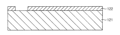
図3を参照すると、本実施例による半導体パッケージは絶縁材質の基板121上に絶縁層122を形成させる段階を含むことができる。
Referring to FIG. 3, the semiconductor package according to the present embodiment may include forming an
このとき、絶縁層122は基板121上に形成されたパッドが外部に露出するように開放されて形成されることができる。また、絶縁層122は感光性材質であることができ、ポリイミド(Polyimide)、ポリベンゾオキサゾール(Polybenzooxazole)、ベンゾシクロブテン(benzocyclobutene)及びエポキシ(epoxy)から成る群から選ばれた1つまたはそれ以上を含むことができる。しかし、絶縁層122の材質はこれに限定されない。
At this time, the insulating
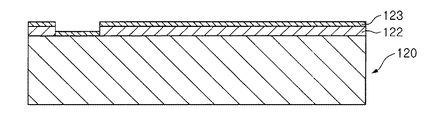
また、図4に図示されたように、上記絶縁層122が形成された半導体チップ120の一面には銅(Cu)材質のメッキ層123を上記絶縁層上にスパッタリング(sputtering)して形成させる段階を含むことができる。
Also, as shown in FIG. 4, a copper (Cu)
従って、メッキ層123は半導体チップ120の前面に全体的に形成されることができ、絶縁層122が開放された部分にも形成されることができる。
Therefore, the
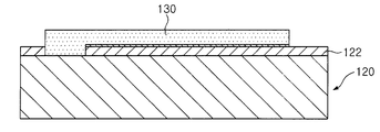
また、図5に図示されたように、フォトレジスト層124を半導体チップ120の一面に形成させた後に、マスクを利用して電極パターン部130が形成される部分のフォトレジスト層124を除去する。
Further, as illustrated in FIG. 5, after the
また、図6に図示されたように、フォトレジスト層124の間には電解メッキ方式により電極パターン部130が形成される。このとき、電極パターン部130は一般的に電気メッキまたはスパッタリングにより形成されることができる。
Also, as shown in FIG. 6,
このとき、電極パターン部130の厚さは約5〜15μmであることを特徴とすることができる。従って、このような厚さで形成される電極パターン部130によって半導体チップ120は電気抵抗が減少することができる。また、このような電極パターン部130により電気的な信頼性が向上するという効果がある。
At this time, the
また、図7に図示されたように、電極パターン部130が形成されない部分のメッキ層123とフォトレジスト層124は除去される。このとき、除去する方法はエッチング工程やストリップ(strip)工程により行われる。
Further, as shown in FIG. 7, the
また、図8に図示されたように、電極パターン部130が形成された半導体チップ120の上部には保護部140を形成する。このとき、保護部140はシリコン窒化層、シリコン酸化層、シリコン酸窒化層またはこれらの多重層であることができる。従って、保護部140により電極パターン部130及び他の回路パターンを保護することができる。
In addition, as illustrated in FIG. 8, the
また、保護部140の一側は、電極パターン部130が露出するように開放して形成され、上記開放された部分にはビア部116が連結される。
In addition, one side of the
従って、上記のように形成された半導体チップ120は、収容空間が設けられる回路基板110に実装され半導体パッケージが完成する。このように製造される半導体パッケージはウェーハの厚さを薄くする工程と、ダイシング(dicing)工程により1つの製品として完成する。
Therefore, the
結果的に、本実施例による半導体パッケージは半導体チップ120の上部に別途のバンプ層を必要としないため、バンプ層を製造する工程である銅メッキ層を形成させる工程と、バンプ層を形成させるためのフォトレジスト層を設ける工程と、上記フォトレジスト層にパターンを形成する工程、バンプメッキ工程と、フォトレジスト及び銅メッキ層を除去する工程等を全て省略することができる。
As a result, since the semiconductor package according to the present embodiment does not require a separate bump layer on the
従って、本実施例による半導体パッケージは、その製造工程が非常に単純化し、大きな経済的利益がある。また、このような工程数の減少は半導体パッケージの製造の歩留まりを向上させる大きな役割をする。 Therefore, the semiconductor package according to the present embodiment has a greatly simplified manufacturing process and a great economic benefit. In addition, such a reduction in the number of processes plays a major role in improving the yield of semiconductor package manufacturing.
100 半導体パッケージ
110 回路基板
116 ビア部
117 ビアホール
120 半導体チップ
121 基板
122 絶縁層
123 メッキ層
124 フォトレジスト層
130 電極パターン部
140 保護部
DESCRIPTION OF
Claims (9)
上記回路基板の収容空間に挿入される半導体チップと、
上記半導体チップの一面にパターン状で形成され、上記回路基板のビア部と直接接触されて互いに電気的に連結される電極パターン部と、
を含む半導体パッケージ。 A circuit board in which a housing space is formed, and
A semiconductor chip inserted into the accommodation space of the circuit board;
An electrode pattern part formed in a pattern on one surface of the semiconductor chip and in direct contact with the via part of the circuit board and electrically connected to each other;
Including semiconductor package.
表面に形成され上記電極パターン部を保護するための保護部を含むことを特徴とする請求項1または2に記載の半導体パッケージ。 The semiconductor chip is
3. The semiconductor package according to claim 1, further comprising a protection part formed on a surface for protecting the electrode pattern part. 4.
上記ビア部と接触する上記電極パターン部の部分が外部に露出するように開放されることを特徴とする請求項3に記載の半導体パッケージ。 The protective part is
4. The semiconductor package according to claim 3, wherein a portion of the electrode pattern portion that contacts the via portion is opened so as to be exposed to the outside.
表面と上記電極パターン部との間に形成される絶縁層を含むことを特徴とする請求項1から4の何れか1項に記載の半導体パッケージ。 The semiconductor chip is
5. The semiconductor package according to claim 1, further comprising an insulating layer formed between a surface and the electrode pattern portion.
上記絶縁層上に、内側に収容空間が形成された回路基板と連結するように再配線メッキして電極パターン部を形成する段階と、
上記電極パターン部が一部露出するように上記再配線メッキの上部に保護部を形成させて半導体チップを製造する段階と、
前記回路基板に上記半導体チップを実装して電気的に連結する段階と、
を含む半導体パッケージの製造方法。 Forming an insulating layer on the substrate;
On the insulating layer, a step of forming an electrode pattern portion by rewiring plating so as to be connected to a circuit board having an accommodation space formed inside,
A step of manufacturing a semiconductor chip by forming a protective part on top of the rewiring plating so that the electrode pattern part is partially exposed;
Mounting and electrically connecting the semiconductor chip to the circuit board;
A method for manufacturing a semiconductor package comprising:
銅(Cu)層を上記絶縁層上にスパッタリング(sputtering)して形成する段階を含むことを特徴とする請求項6または7に記載の半導体パッケージの製造方法。 The step of forming the electrode pattern portion includes:
8. The method of manufacturing a semiconductor package according to claim 6, further comprising a step of forming a copper (Cu) layer on the insulating layer by sputtering.
上記回路基板から上記電極パターン部の上部まで連結されるビアホールを形成した後に、上記ビアホールに導電物質を充填して電気的に連結されるビア部を形成する段階を含むことを特徴とする請求項6から8の何れか1項に記載の半導体パッケージの製造方法。 Electrically connecting the semiconductor chip to the circuit board comprises:
2. The method of claim 1, further comprising forming a via portion that is electrically connected by filling the via hole with a conductive material after forming a via hole connected from the circuit board to an upper portion of the electrode pattern portion. The method for manufacturing a semiconductor package according to any one of 6 to 8.
Applications Claiming Priority (2)
| Application Number | Priority Date | Filing Date | Title |
|---|---|---|---|
| KR10-2009-0109027 | 2009-11-12 | ||
| KR1020090109027A KR101113501B1 (en) | 2009-11-12 | 2009-11-12 | Manufacturing method of semiconductor package |
Related Parent Applications (1)
| Application Number | Title | Priority Date | Filing Date |
|---|---|---|---|
| JP2010167116A Division JP2011109060A (en) | 2009-11-12 | 2010-07-26 | Semiconductor package and method for manufacturing the same |
Publications (1)
| Publication Number | Publication Date |
|---|---|
| JP2012256919A true JP2012256919A (en) | 2012-12-27 |
Family
ID=43973556
Family Applications (2)
| Application Number | Title | Priority Date | Filing Date |
|---|---|---|---|
| JP2010167116A Pending JP2011109060A (en) | 2009-11-12 | 2010-07-26 | Semiconductor package and method for manufacturing the same |
| JP2012174235A Pending JP2012256919A (en) | 2009-11-12 | 2012-08-06 | Manufacturing method for semiconductor package |
Family Applications Before (1)
| Application Number | Title | Priority Date | Filing Date |
|---|---|---|---|
| JP2010167116A Pending JP2011109060A (en) | 2009-11-12 | 2010-07-26 | Semiconductor package and method for manufacturing the same |
Country Status (3)
| Country | Link |
|---|---|
| US (2) | US20110108993A1 (en) |
| JP (2) | JP2011109060A (en) |
| KR (1) | KR101113501B1 (en) |
Families Citing this family (1)
| Publication number | Priority date | Publication date | Assignee | Title |
|---|---|---|---|---|
| JP5826532B2 (en) * | 2010-07-15 | 2015-12-02 | 新光電気工業株式会社 | Semiconductor device and manufacturing method thereof |
Citations (3)
| Publication number | Priority date | Publication date | Assignee | Title |
|---|---|---|---|---|
| JP2005150452A (en) * | 2003-11-17 | 2005-06-09 | Fujikura Ltd | Method for manufacturing semiconductor package |
| JP2007214402A (en) * | 2006-02-10 | 2007-08-23 | Cmk Corp | Semiconductor element and printed wiring board with built-in semiconductor element |
| JP2008124247A (en) * | 2006-11-13 | 2008-05-29 | Toppan Printing Co Ltd | Substrate with built-in component and its manufacturing method |
Family Cites Families (32)
| Publication number | Priority date | Publication date | Assignee | Title |
|---|---|---|---|---|
| DE60128656T2 (en) * | 2000-02-25 | 2007-10-04 | Ibiden Co., Ltd., Ogaki | MULTILAYER CONDUCTOR PLATE AND METHOD FOR THE PRODUCTION THEREOF |
| KR20010105641A (en) * | 2000-05-17 | 2001-11-29 | 윤종용 | Wafer level chip scale package and manufacturing method thereof |
| US6686653B2 (en) * | 2000-06-28 | 2004-02-03 | Institut National D'optique | Miniature microdevice package and process for making thereof |
| US6573592B2 (en) * | 2001-08-21 | 2003-06-03 | Micron Technology, Inc. | Semiconductor die packages with standard ball grid array footprint and method for assembling the same |
| TWI280641B (en) * | 2001-12-28 | 2007-05-01 | Via Tech Inc | Chip structure |
| SG104293A1 (en) * | 2002-01-09 | 2004-06-21 | Micron Technology Inc | Elimination of rdl using tape base flip chip on flex for die stacking |
| US20030160335A1 (en) * | 2002-02-27 | 2003-08-28 | Ho-Ming Tong | Flip chip interconnection structure and fabrication process thereof |
| US6939789B2 (en) * | 2002-05-13 | 2005-09-06 | Taiwan Semiconductor Manufacturing Co., Ltd. | Method of wafer level chip scale packaging |
| KR100546346B1 (en) * | 2003-07-23 | 2006-01-26 | 삼성전자주식회사 | Method for forming redistribution bump, semiconductor chip and mount structure fabricated using same |
| JP3904541B2 (en) * | 2003-09-26 | 2007-04-11 | 沖電気工業株式会社 | Manufacturing method of semiconductor device embedded substrate |
| JP2005327984A (en) * | 2004-05-17 | 2005-11-24 | Shinko Electric Ind Co Ltd | Electronic component and method of manufacturing electronic-component mounting structure |
| JP4907070B2 (en) * | 2004-09-10 | 2012-03-28 | ルネサスエレクトロニクス株式会社 | Semiconductor device and manufacturing method thereof |
| KR100618892B1 (en) * | 2005-04-13 | 2006-09-01 | 삼성전자주식회사 | Semiconductor package accomplishing a fan-out structure through wire bonding |
| US7449365B2 (en) * | 2005-11-09 | 2008-11-11 | Broadcom Corporation | Wafer-level flipchip package with IC circuit isolation |
| US7728437B2 (en) * | 2005-11-23 | 2010-06-01 | Fairchild Korea Semiconductor, Ltd. | Semiconductor package form within an encapsulation |
| JP2007220803A (en) * | 2006-02-15 | 2007-08-30 | Shinko Electric Ind Co Ltd | Multilayer wiring board and its connection method |
| US7727876B2 (en) * | 2006-12-21 | 2010-06-01 | Stats Chippac, Ltd. | Semiconductor device and method of protecting passivation layer in a solder bump process |
| KR20080085380A (en) * | 2007-03-19 | 2008-09-24 | 삼성전자주식회사 | Semiconductor package having wire redistribution layer and method of fabricating the same |
| KR100945285B1 (en) * | 2007-09-18 | 2010-03-03 | 삼성전기주식회사 | Electronic components embedded PCB and method for manufacturing thereof |
| US7667335B2 (en) * | 2007-09-20 | 2010-02-23 | Stats Chippac, Ltd. | Semiconductor package with passivation island for reducing stress on solder bumps |
| US20090127686A1 (en) * | 2007-11-21 | 2009-05-21 | Advanced Chip Engineering Technology Inc. | Stacking die package structure for semiconductor devices and method of the same |
| US8035210B2 (en) * | 2007-12-28 | 2011-10-11 | Stats Chippac Ltd. | Integrated circuit package system with interposer |
| KR101478247B1 (en) * | 2008-03-12 | 2014-12-31 | 삼성전자주식회사 | semiconductor package and multi-chip package using the same |
| US20090230554A1 (en) * | 2008-03-13 | 2009-09-17 | Broadcom Corporation | Wafer-level redistribution packaging with die-containing openings |
| JP2009239247A (en) * | 2008-03-27 | 2009-10-15 | Ibiden Co Ltd | Method of manufacturing multilayer printed circuit board |
| US20090294958A1 (en) * | 2008-05-30 | 2009-12-03 | Broadcom Corporation | Wafer level redistribution using circuit printing technology |
| US20090294961A1 (en) * | 2008-06-02 | 2009-12-03 | Infineon Technologies Ag | Semiconductor device |
| US8014166B2 (en) * | 2008-09-06 | 2011-09-06 | Broadpak Corporation | Stacking integrated circuits containing serializer and deserializer blocks using through silicon via |
| JP5102726B2 (en) * | 2008-09-08 | 2012-12-19 | ラピスセミコンダクタ株式会社 | Manufacturing method of semiconductor device |
| US20100133682A1 (en) * | 2008-12-02 | 2010-06-03 | Infineon Technologies Ag | Semiconductor device |
| US8624370B2 (en) * | 2009-03-20 | 2014-01-07 | Stats Chippac Ltd. | Integrated circuit packaging system with an interposer and method of manufacture thereof |
| JP2011146547A (en) * | 2010-01-15 | 2011-07-28 | Murata Mfg Co Ltd | Circuit module |
-
2009
- 2009-11-12 KR KR1020090109027A patent/KR101113501B1/en active IP Right Grant
-
2010
- 2010-07-26 JP JP2010167116A patent/JP2011109060A/en active Pending
- 2010-07-26 US US12/805,334 patent/US20110108993A1/en not_active Abandoned
-
2012
- 2012-07-25 US US13/557,362 patent/US20120295404A1/en not_active Abandoned
- 2012-08-06 JP JP2012174235A patent/JP2012256919A/en active Pending
Patent Citations (3)
| Publication number | Priority date | Publication date | Assignee | Title |
|---|---|---|---|---|
| JP2005150452A (en) * | 2003-11-17 | 2005-06-09 | Fujikura Ltd | Method for manufacturing semiconductor package |
| JP2007214402A (en) * | 2006-02-10 | 2007-08-23 | Cmk Corp | Semiconductor element and printed wiring board with built-in semiconductor element |
| JP2008124247A (en) * | 2006-11-13 | 2008-05-29 | Toppan Printing Co Ltd | Substrate with built-in component and its manufacturing method |
Also Published As
| Publication number | Publication date |
|---|---|
| JP2011109060A (en) | 2011-06-02 |
| US20120295404A1 (en) | 2012-11-22 |
| US20110108993A1 (en) | 2011-05-12 |
| KR101113501B1 (en) | 2012-02-29 |
| KR20110052112A (en) | 2011-05-18 |
Similar Documents
| Publication | Publication Date | Title |
|---|---|---|
| US11961867B2 (en) | Electronic device package and fabricating method thereof | |
| JP4934053B2 (en) | Semiconductor device and manufacturing method thereof | |
| CN110085523B (en) | Semiconductor device and method for manufacturing the same | |
| US8922013B2 (en) | Through via package | |
| KR100835277B1 (en) | Fabrication method of electronic device having a sacrificial anode and electronic device fabricated thereby | |
| US8309860B2 (en) | Electronic component built-in substrate and method of manufacturing the same | |
| JP2008182224A (en) | Stack package and its manufacturing method | |
| US20120097430A1 (en) | Packaging substrate and method of fabricating the same | |
| KR101060842B1 (en) | Manufacturing method of semiconductor package | |
| JP2009164607A (en) | Bonding pad structure, manufacturing method thereof, and semiconductor package including bonding pad structure | |
| KR20150073864A (en) | Integrated circuit packging system with vialess substrate and method of manufacture thereof | |
| JP2009176978A (en) | Semiconductor device | |
| KR100826989B1 (en) | Semiconductor package and method for fabricating the same | |
| KR100787892B1 (en) | Semiconductor package and methods of manufacturing the same | |
| KR20100095901A (en) | Stack type semiconductor package | |
| US7193297B2 (en) | Semiconductor device, method for manufacturing the same, circuit substrate and electronic device | |
| US10115704B2 (en) | Semiconductor device | |
| JP2012256919A (en) | Manufacturing method for semiconductor package | |
| KR20080038719A (en) | Semiconductor device and method for manufacturing the same | |
| JP4728079B2 (en) | Semiconductor device substrate and semiconductor device | |
| KR20130050077A (en) | Stacked package and method of manufacturing the semiconductor package | |
| US8603911B2 (en) | Semiconductor device and fabrication method thereof | |
| KR20090114492A (en) | Semiconductor device and method for manufacturing the same | |
| JP2008124301A (en) | Semiconductor and its manufacturing method | |
| KR101212794B1 (en) | Semiconductor pacakge and method of manufacturing the same |
Legal Events
| Date | Code | Title | Description |
|---|---|---|---|
| A621 | Written request for application examination |
Free format text: JAPANESE INTERMEDIATE CODE: A621 Effective date: 20130430 |
|
| A977 | Report on retrieval |
Free format text: JAPANESE INTERMEDIATE CODE: A971007 Effective date: 20130730 |
|
| A131 | Notification of reasons for refusal |
Free format text: JAPANESE INTERMEDIATE CODE: A131 Effective date: 20130806 |
|
| A02 | Decision of refusal |
Free format text: JAPANESE INTERMEDIATE CODE: A02 Effective date: 20140128 |