JP2012253217A - Semiconductor module and method of manufacturing the same - Google Patents
Semiconductor module and method of manufacturing the same Download PDFInfo
- Publication number
- JP2012253217A JP2012253217A JP2011125141A JP2011125141A JP2012253217A JP 2012253217 A JP2012253217 A JP 2012253217A JP 2011125141 A JP2011125141 A JP 2011125141A JP 2011125141 A JP2011125141 A JP 2011125141A JP 2012253217 A JP2012253217 A JP 2012253217A
- Authority
- JP
- Japan
- Prior art keywords
- semiconductor device
- power semiconductor
- main surface
- base material
- semiconductor devices
- Prior art date
- Legal status (The legal status is an assumption and is not a legal conclusion. Google has not performed a legal analysis and makes no representation as to the accuracy of the status listed.)
- Withdrawn
Links
Images


Classifications
-
- H—ELECTRICITY
- H01—ELECTRIC ELEMENTS
- H01L—SEMICONDUCTOR DEVICES NOT COVERED BY CLASS H10
- H01L2224/00—Indexing scheme for arrangements for connecting or disconnecting semiconductor or solid-state bodies and methods related thereto as covered by H01L24/00
- H01L2224/01—Means for bonding being attached to, or being formed on, the surface to be connected, e.g. chip-to-package, die-attach, "first-level" interconnects; Manufacturing methods related thereto
- H01L2224/26—Layer connectors, e.g. plate connectors, solder or adhesive layers; Manufacturing methods related thereto
- H01L2224/31—Structure, shape, material or disposition of the layer connectors after the connecting process
- H01L2224/32—Structure, shape, material or disposition of the layer connectors after the connecting process of an individual layer connector
- H01L2224/321—Disposition
- H01L2224/32151—Disposition the layer connector connecting between a semiconductor or solid-state body and an item not being a semiconductor or solid-state body, e.g. chip-to-substrate, chip-to-passive
- H01L2224/32221—Disposition the layer connector connecting between a semiconductor or solid-state body and an item not being a semiconductor or solid-state body, e.g. chip-to-substrate, chip-to-passive the body and the item being stacked
- H01L2224/32245—Disposition the layer connector connecting between a semiconductor or solid-state body and an item not being a semiconductor or solid-state body, e.g. chip-to-substrate, chip-to-passive the body and the item being stacked the item being metallic
-
- H—ELECTRICITY
- H01—ELECTRIC ELEMENTS
- H01L—SEMICONDUCTOR DEVICES NOT COVERED BY CLASS H10
- H01L2224/00—Indexing scheme for arrangements for connecting or disconnecting semiconductor or solid-state bodies and methods related thereto as covered by H01L24/00
- H01L2224/01—Means for bonding being attached to, or being formed on, the surface to be connected, e.g. chip-to-package, die-attach, "first-level" interconnects; Manufacturing methods related thereto
- H01L2224/42—Wire connectors; Manufacturing methods related thereto
- H01L2224/47—Structure, shape, material or disposition of the wire connectors after the connecting process
- H01L2224/48—Structure, shape, material or disposition of the wire connectors after the connecting process of an individual wire connector
- H01L2224/4805—Shape
- H01L2224/4809—Loop shape
- H01L2224/48091—Arched
-
- H—ELECTRICITY
- H01—ELECTRIC ELEMENTS
- H01L—SEMICONDUCTOR DEVICES NOT COVERED BY CLASS H10
- H01L2224/00—Indexing scheme for arrangements for connecting or disconnecting semiconductor or solid-state bodies and methods related thereto as covered by H01L24/00
- H01L2224/01—Means for bonding being attached to, or being formed on, the surface to be connected, e.g. chip-to-package, die-attach, "first-level" interconnects; Manufacturing methods related thereto
- H01L2224/42—Wire connectors; Manufacturing methods related thereto
- H01L2224/47—Structure, shape, material or disposition of the wire connectors after the connecting process
- H01L2224/48—Structure, shape, material or disposition of the wire connectors after the connecting process of an individual wire connector
- H01L2224/481—Disposition
- H01L2224/48151—Connecting between a semiconductor or solid-state body and an item not being a semiconductor or solid-state body, e.g. chip-to-substrate, chip-to-passive
- H01L2224/48221—Connecting between a semiconductor or solid-state body and an item not being a semiconductor or solid-state body, e.g. chip-to-substrate, chip-to-passive the body and the item being stacked
- H01L2224/48245—Connecting between a semiconductor or solid-state body and an item not being a semiconductor or solid-state body, e.g. chip-to-substrate, chip-to-passive the body and the item being stacked the item being metallic
- H01L2224/48247—Connecting between a semiconductor or solid-state body and an item not being a semiconductor or solid-state body, e.g. chip-to-substrate, chip-to-passive the body and the item being stacked the item being metallic connecting the wire to a bond pad of the item
-
- H—ELECTRICITY
- H01—ELECTRIC ELEMENTS
- H01L—SEMICONDUCTOR DEVICES NOT COVERED BY CLASS H10
- H01L2224/00—Indexing scheme for arrangements for connecting or disconnecting semiconductor or solid-state bodies and methods related thereto as covered by H01L24/00
- H01L2224/73—Means for bonding being of different types provided for in two or more of groups H01L2224/10, H01L2224/18, H01L2224/26, H01L2224/34, H01L2224/42, H01L2224/50, H01L2224/63, H01L2224/71
- H01L2224/732—Location after the connecting process
- H01L2224/73251—Location after the connecting process on different surfaces
- H01L2224/73265—Layer and wire connectors
-
- H—ELECTRICITY
- H01—ELECTRIC ELEMENTS
- H01L—SEMICONDUCTOR DEVICES NOT COVERED BY CLASS H10
- H01L2924/00—Indexing scheme for arrangements or methods for connecting or disconnecting semiconductor or solid-state bodies as covered by H01L24/00
- H01L2924/10—Details of semiconductor or other solid state devices to be connected
- H01L2924/11—Device type
- H01L2924/13—Discrete devices, e.g. 3 terminal devices
- H01L2924/1304—Transistor
- H01L2924/1305—Bipolar Junction Transistor [BJT]
- H01L2924/13055—Insulated gate bipolar transistor [IGBT]
-
- H—ELECTRICITY
- H01—ELECTRIC ELEMENTS
- H01L—SEMICONDUCTOR DEVICES NOT COVERED BY CLASS H10
- H01L2924/00—Indexing scheme for arrangements or methods for connecting or disconnecting semiconductor or solid-state bodies as covered by H01L24/00
- H01L2924/10—Details of semiconductor or other solid state devices to be connected
- H01L2924/11—Device type
- H01L2924/13—Discrete devices, e.g. 3 terminal devices
- H01L2924/1304—Transistor
- H01L2924/1306—Field-effect transistor [FET]
- H01L2924/13091—Metal-Oxide-Semiconductor Field-Effect Transistor [MOSFET]
Abstract
Description
本発明は、半導体モジュールおよびその製造技術に関し、例えば電力の変換や制御を行うパワー半導体デバイスおよびパワー半導体デバイスと電気的に接続される電子部品を一つの基材に搭載した半導体モジュールに適用して有効な技術に関するものである。 The present invention relates to a semiconductor module and a manufacturing technique thereof, and is applied to, for example, a power semiconductor device that performs power conversion and control and a semiconductor module in which an electronic component that is electrically connected to the power semiconductor device is mounted on a single substrate. It relates to effective technology.
特開平7−236281号公報(特許文献1)には、ボードの一方の面に複数のパワーモジュールを配置し、他方の面に複数の抵抗器およびコンデンサを取り付け、複数のパワーモジュールのそれぞれを冷却フィンに接触させる構成が記載されている。 In Japanese Patent Laid-Open No. 7-236281 (Patent Document 1), a plurality of power modules are arranged on one surface of a board, a plurality of resistors and capacitors are attached to the other surface, and each of the plurality of power modules is cooled. A configuration for contacting the fin is described.
電子装置は、複数の電子部品を実装基板に搭載し、これらを電気的に接続することでシステムを構成する。また複数のシステムを組み合わせることで電子装置に様々な機能を付加することができる。しかし、電子装置の多機能化を図る場合、使用する電子部品の数が多くなるので、電子部品の実装作業が煩雑になる。また、実装基板における配線設計が煩雑になる。また、電子装置の製造コストが上昇する。上記課題に対応する方法として、例えばシステム単位で必要な複数の電子部品を一つの基材(インタポーザ)に搭載することによりモジュール化し、必要なモジュール(システムモジュール)を選択して実装基板に実装する技術が有効である。 An electronic device is configured by mounting a plurality of electronic components on a mounting board and electrically connecting them. Various functions can be added to the electronic device by combining a plurality of systems. However, when the number of electronic devices is increased, the number of electronic components to be used increases, and the mounting work of the electronic components becomes complicated. Further, the wiring design on the mounting board becomes complicated. In addition, the manufacturing cost of the electronic device increases. As a method for addressing the above problems, for example, a plurality of necessary electronic components in units of systems are modularized by mounting them on one base material (interposer), and necessary modules (system modules) are selected and mounted on a mounting board. Technology is effective.
本願発明者は上記モジュール化技術について検討を行い、以下の課題を見出した。すなわち、モジュールに搭載する各電子部品のレイアウトによっては、モジュールの信頼性が低下する。例えば、電力の変換や制御を行うパワー半導体デバイス(半導体装置)およびパワー半導体デバイスと電気的に接続される電子部品を一つの基材に搭載したパワーモジュール(半導体モジュール)の場合、例えば1A(アンペア)以上の大電流が流れるため、発熱量が大きくなる。このため、パワーモジュールの主たる熱源を効率的に冷却しなければ熱影響によりモジュールの信頼性が低下する。また、モジュールの組み立て工程の効率が低下すれば、モジュールの製造コストが上昇するので、モジュール化のメリットが低下する。 The inventor of the present application has studied the above modularization technique and found the following problems. That is, depending on the layout of each electronic component mounted on the module, the reliability of the module decreases. For example, in the case of a power module (semiconductor module) in which a power semiconductor device (semiconductor device) that performs power conversion and control and an electronic component that is electrically connected to the power semiconductor device are mounted on one substrate, for example, 1A (ampere) ) A large amount of current flows, so the amount of heat generation increases. For this reason, if the main heat source of a power module is not cooled efficiently, the reliability of a module will fall by a thermal effect. Further, if the efficiency of the module assembly process is reduced, the manufacturing cost of the module is increased, so that the merit of modularization is reduced.
本発明は、上記課題に鑑みてなされたものであり、その目的は、パワー半導体デバイスを含む、複数の電子部品を搭載した半導体モジュールの信頼性を向上させる技術を提供することにある。 The present invention has been made in view of the above problems, and an object of the present invention is to provide a technique for improving the reliability of a semiconductor module including a plurality of electronic components including a power semiconductor device.
また、本発明の他の目的は、上記半導体モジュールを効率的に製造する技術を提供することにある。 Another object of the present invention is to provide a technique for efficiently manufacturing the semiconductor module.
本発明の前記ならびにその他の目的と新規な特徴は、本明細書の記述および添付図面から明らかになるであろう。 The above and other objects and novel features of the present invention will be apparent from the description of this specification and the accompanying drawings.
本願において開示される発明のうち、代表的なものの概要を簡単に説明すれば、次のとおりである。 Of the inventions disclosed in the present application, the outline of typical ones will be briefly described as follows.
すなわち、本願発明の一態様である半導体モジュールは、第1主面、前記第1主面とは反対側に位置する第2主面を有し、基材の一方の搭載面に搭載されるパワー半導体デバイスを含み、側面視において、前記基材の搭載面側では、前記パワー半導体デバイスの前記第2主面が前記搭載面から最も離れた位置に配置されている。また、前記パワー半導体デバイスには、前記第1主面、前記第2主面のうち、いずれか一方から他方まで貫通する貫通孔が形成され、前記パワー半導体デバイスは、平面視において、前記貫通孔が前記基材の外側に配置されるものである。 That is, the semiconductor module which is one aspect of the present invention has a first main surface and a second main surface located on the opposite side of the first main surface, and is mounted on one mounting surface of the substrate. In the side view, including the semiconductor device, the second main surface of the power semiconductor device is disposed at a position farthest from the mounting surface on the mounting surface side of the base material. Further, the power semiconductor device is formed with a through hole penetrating from one of the first main surface and the second main surface to the other, and the power semiconductor device has the through hole in a plan view. Is arranged outside the substrate.
本願において開示される発明のうち、代表的なものによって得られる効果を簡単に説明すれば以下の通りである。 The effects obtained by typical ones of the inventions disclosed in the present application will be briefly described as follows.
すなわち、本願発明の一態様によれば、半導体デバイスを含む、複数の電子部品を搭載した半導体装置(モジュール)の信頼性を向上させることができる。 That is, according to one embodiment of the present invention, the reliability of a semiconductor device (module) including a plurality of electronic components including a semiconductor device can be improved.
(本願における記載形式・基本的用語・用法の説明)
本願において、実施の態様の記載は、必要に応じて、便宜上複数のセクション等に分けて記載するが、特にそうでない旨明示した場合を除き、これらは相互に独立別個のものではなく、記載の前後を問わず、単一の例の各部分、一方が他方の一部詳細または一部または全部の変形例等である。また、原則として、同様の部分は繰り返しの説明を省略する。また、実施の態様における各構成要素は、特にそうでない旨明示した場合、理論的にその数に限定される場合および文脈から明らかにそうでない場合を除き、必須のものではない。
(Description format, basic terms, usage in this application)
In the present application, the description of the embodiment will be divided into a plurality of sections for convenience, if necessary, but these are not independent from each other unless otherwise specified. Regardless of the front and rear, each part of a single example, one is a part of the other, or a part or all of the modifications. In principle, repeated description of similar parts is omitted. In addition, each component in the embodiment is not indispensable unless specifically stated otherwise, unless it is theoretically limited to the number, and obviously not in context.
同様に実施の態様等の記載において、材料、組成等について、「AからなるX」等といっても、特にそうでない旨明示した場合および文脈から明らかにそうでない場合を除き、A以外の要素を含むものを排除するものではない。たとえば、成分についていえば、「Aを主要な成分として含むX」等の意味である。たとえば、「シリコン部材」等といっても、純粋なシリコンに限定されるものではなく、SiGe(シリコン・ゲルマニウム)合金やその他シリコンを主要な成分とする多元合金、その他の添加物等を含む部材も含むものであることはいうまでもない。また、金めっき、Cu層、ニッケル・めっき等といっても、そうでない旨、特に明示した場合を除き、純粋なものだけでなく、それぞれ金、Cu、ニッケル等を主要な成分とする部材を含むものとする。 Similarly, in the description of the embodiment, etc., regarding the material, composition, etc., “X consisting of A” etc. is an element other than A unless specifically stated otherwise and clearly not in context. It does not exclude things that contain. For example, as for the component, it means “X containing A as a main component”. For example, “silicon member” is not limited to pure silicon, but includes a SiGe (silicon-germanium) alloy, other multi-component alloys containing silicon as a main component, and other additives. Needless to say, it is also included. Moreover, even if it says gold plating, Cu layer, nickel / plating, etc., unless otherwise specified, not only pure materials but also members mainly composed of gold, Cu, nickel, etc. Shall be included.
さらに、特定の数値、数量に言及したときも、特にそうでない旨明示した場合、理論的にその数に限定される場合および文脈から明らかにそうでない場合を除き、その特定の数値を超える数値であってもよいし、その特定の数値未満の数値でもよい。 In addition, when a specific number or quantity is mentioned, a numerical value exceeding that specific number will be used unless specifically stated otherwise, unless theoretically limited to that number, or unless otherwise clearly indicated by the context. There may be a numerical value less than the specific numerical value.
また、実施の形態の各図中において、同一または同様の部分は同一または類似の記号または参照番号で示し、説明は原則として繰り返さない。 Moreover, in each figure of embodiment, the same or similar part is shown with the same or similar symbol or reference number, and description is not repeated in principle.
また、添付図面においては、却って、煩雑になる場合または空隙との区別が明確である場合には、断面であってもハッチング等を省略する場合がある。これに関連して、説明等から明らかである場合等には、平面的に閉じた孔であっても、背景の輪郭線を省略する場合がある。更に、断面でなくとも、空隙でないことを明示するため、あるいは領域の境界を明示するために、ハッチングやドットパターンを付すことがある。 In the accompanying drawings, hatching or the like may be omitted even in a cross section when it becomes complicated or when the distinction from the gap is clear. In relation to this, when it is clear from the description etc., the contour line of the background may be omitted even if the hole is planarly closed. Furthermore, even if it is not a cross section, hatching or a dot pattern may be added in order to clearly indicate that it is not a void or to clearly indicate the boundary of a region.
(実施の形態1)
本実施の形態では、パワー半導体デバイスを含む、複数の電子部品を搭載した半導体モジュールの一例として、例えば、電磁調理器具などの家庭用電気器具の電源回路に組み込まれる電力変換装置(インバータ)に用いるモジュールを取り上げて説明する。図1は、本実施の形態の半導体モジュールを含む電力変換装置の例を示す回路図である。
(Embodiment 1)
In this embodiment, as an example of a semiconductor module including a plurality of electronic components including a power semiconductor device, for example, it is used for a power conversion device (inverter) incorporated in a power supply circuit of a household electric appliance such as an electromagnetic cooking appliance. Describes the module. FIG. 1 is a circuit diagram showing an example of a power conversion device including the semiconductor module of the present embodiment.
<電力変換装置>
電力変換装置1は、例えば電磁調理器具などの家庭用電気器具の電源回路に用いられており、半導体モジュール2と、制御回路3と、入力コンデンサCinと、出力コンデンサCoutと、コイルLとを有している。なお、符号のVINは入力電源、GNDは基準電位(例えばグランド電位で0V)、Ioutは出力電流、Voutは出力電圧を示している。
<Power conversion device>
The
半導体モジュール2は、2つのドライバ回路(駆動回路)DR1、DR2と、2つのパワートランジスタQH1、QL1とを有している。2つのドライバ回路DR1、DR2は、一つの半導体装置(電子部品)PDR内に封止(収容)されている。また、パワートランジスタQH1、QL1は、それぞれ独立した半導体装置(電子部品、パッケージ、パワー半導体デバイス)PAH、PAL内に封止(収容)されている。また、半導体モジュール2は、4つの抵抗素子RH1、RH2、RL1、RL2および一つのダイオード素子D1を有している。抵抗素子RH1、RH2は、パワートランジスタQH1のバイアス回路を構成し、抵抗素子RL1、RL2は、パワートランジスタQL1のバイアス回路を構成する。これら4つの抵抗素子RH1、RH2、RL1、RL2および一つのダイオード素子D1は、それぞれ独立した電子部品として構成され、半導体モジュール2の基材である配線基板に搭載され、配線基板に形成された配線を介して電気的に接続されている。パワートランジスタは、電源回路等に組み込まれ、電力の変換や制御を行う回路を構成する半導体素子であって、例えば、パワーMOSFET(Metal Oxide Semiconductor Field Effect Transistor)や、絶縁ゲートバイポーラトランジスタ(IGBT;Insulated Gate Bipolar Transistor)がこれに相当する。パワートランジスタには、例えば1A(アンペア)以上の大電流が流れるため、パワートランジスタは、並列接続で電気的に接続した複数のトランジスタ素子で構成される。本実施の形態では、電力変換回路に組み込まれるスイッチング素子として、IGBTである2つのパワートランジスタQH1、QL1を用いた例について説明する。
The
ドライバ回路DR1、DR2は、上記制御回路3から供給された制御信号に応じて、それぞれパワートランジスタQH1、QL1のゲート端子Gの電位を制御し、パワートランジスタQH1、QL1の動作を制御する回路である。一方のドライバ回路DR1の出力は、パワートランジスタQH1のゲート端子Gに電気的に接続されている。他方のドライバ回路DR2の出力は、パワートランジスタQL1のゲート端子Gに電気的に接続されている。図1に示す例では、この2つのドライバ回路DR1、DR2は、例えば、同一の半導体チップに形成されている。そして、この2つのドライバ回路DR1、DR2が形成された半導体チップは半導体装置PDRに内蔵されている。
The driver circuits DR1 and DR2 are circuits for controlling the operation of the power transistors QH1 and QL1 by controlling the potentials of the gate terminals G of the power transistors QH1 and QL1 according to the control signal supplied from the
上記パワートランジスタQH1、QL1は、入力電源VINの高電位(第1の電源電位)供給用の端子(第1電源端子)ET1と、基準電位(第2の電源電位)GND供給用の端子(第2電源端子)ET2との間に直列に接続されている。すなわち、パワートランジスタQH1は、そのエミッタ・コレクタ経路が、入力電源VINの高電位供給用の端子ET1と出力ノード(出力端子)Nとの間に直列に接続され、パワートランジスタQL1は、そのエミッタ・コレクタ経路が出力ノードNと基準電位GND供給用の端子ET2との間に直列に接続されている。なお、図1では、パワートランジスタQH1、QL1それぞれの寄生ダイオード(内部ダイオード)を図示している。 The power transistors QH1 and QL1 include a terminal (first power supply terminal) ET1 for supplying a high potential (first power supply potential) of the input power supply VIN and a terminal (first power supply potential) GND for supplying a reference potential (second power supply potential). 2 power supply terminals) are connected in series with ET2. That is, the power transistor QH1 has its emitter-collector path connected in series between the high-potential supply terminal ET1 of the input power supply VIN and the output node (output terminal) N. The power transistor QL1 A collector path is connected in series between the output node N and a reference potential GND supply terminal ET2. In FIG. 1, parasitic diodes (internal diodes) of the power transistors QH1 and QL1 are shown.
パワートランジスタQH1は、ハイサイドスイッチ(高電位側:第1動作電圧;以下、単にハイサイドという)用のパワートランジスタであり、上記コイルLにエネルギーを蓄えるためのスイッチ機能を有している。コイルLは、電力変換装置1の出力(負荷LDの入力)に電力を供給する素子である。このハイサイド用のパワートランジスタQH1は、ドライバ回路DR1、DR2が形成された半導体装置PDRとは別の半導体装置PAHに形成されている。 The power transistor QH1 is a power transistor for a high side switch (high potential side: first operating voltage; hereinafter simply referred to as high side), and has a switch function for storing energy in the coil L. The coil L is an element that supplies power to the output of the power conversion device 1 (input of the load LD). The high-side power transistor QH1 is formed in a semiconductor device PAH different from the semiconductor device PDR in which the driver circuits DR1 and DR2 are formed.
一方、パワートランジスタQL1は、ローサイドスイッチ(低電位側:第2動作電圧;以下、単にローサイドという)用のパワートランジスタであり、制御回路3からの周波数に同期してトランジスタの抵抗を低くして整流を行う機能を有している。すなわち、パワートランジスタQL1は、電力変換装置1の整流用のトランジスタである。このローサイド用のパワートランジスタQL1は、ドライバ回路DR1、DR2が形成された半導体装置PDRとは別の半導体装置PALに形成されている。
On the other hand, the power transistor QL1 is a power transistor for a low side switch (low potential side: second operating voltage; hereinafter, simply referred to as low side), and rectifies the transistor by lowering the resistance of the transistor in synchronization with the frequency from the
上記制御回路3は、パワートランジスタQH1、QL1の動作を制御する回路であり、例えばPWM(Pulse Width Modulation)回路によって構成されている。このPWM回路は、指令信号と三角波の振幅とを比較してPWM信号(制御信号)を出力する。このPWM信号により、パワートランジスタQH1、QL1(すなわち、電力変換装置1)の出力電圧(すなわち、パワートランジスタQH1、QL1の電圧スイッチオンの幅(オン時間))が制御されるようになっている。
The
この制御回路3の出力は、ドライバ回路DR1、DR2の入力に電気的に接続されている。ドライバ回路DR1、DR2のそれぞれの出力は、それぞれパワートランジスタQH1のゲート端子GおよびパワートランジスタQL1のゲート端子Gに電気的に接続されている。詳しくは、ドライバ回路DR1の出力は、抵抗素子RH1を介してパワートランジスタQH1のゲート端子Gに電気的に接続されている。また、ドライバ回路DR2の出力は、抵抗素子RL1を介してパワートランジスタQL1のゲート端子Gに電気的に接続されている。
The output of the
上記入力コンデンサCinは、入力電源VINから供給されたエネルギー(電荷)を一時的に蓄えて、その蓄えたエネルギーを電力変換装置1の主回路に供給する電源であり、入力電源VINに並列に電気的に接続されている。上記出力コンデンサCoutは、上記コイルLと負荷LDとを結ぶ出力配線と基準電位GND供給用の端子との間に電気的に接続されている。
The input capacitor Cin is a power source that temporarily stores energy (charge) supplied from the input power source VIN and supplies the stored energy to the main circuit of the
電力変換装置1のパワートランジスタQH1のエミッタと、パワートランジスタQL1のコレクタとを結ぶ配線には、出力用電源電位を外部に供給する上記出力ノードNが設けられている。この出力ノードNは、出力配線を介してコイルLと電気的に接続され、さらに出力配線を介して負荷LDと電気的に接続されている。
The wiring connecting the emitter of the power transistor QH1 and the collector of the power transistor QL1 of the
このような電力変換装置1では、パワートランジスタQH1、QL1で同期を取りながら、このパワートランジスタQH1、QL1を交互にオン/オフすることにより電源電圧の変換を行っている。すなわち、ハイサイド用のパワートランジスタQH1がオンの時、端子ET1からパワートランジスタQH1を通じて出力ノードNに電流(第1電流)I1が流れる。一方、ハイサイド用のパワートランジスタQH1がオフの時、コイルLの逆起電圧により電流I2が流れる。この電流I2が流れている時にローサイド用のパワートランジスタQL1をオンすることで、電圧降下を少なくすることができる。
In such a
<半導体モジュール>
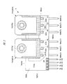
次に、図1に示す半導体モジュール2の構造について説明する。図2は、図1に示す半導体モジュールの一方の面の外観を示す平面図、図3は図2に示す半導体モジュールの反対側の面の外観を示す平面図、図4および図5は、図1および図2に示す半導体モジュールに放熱板を固定した状態を示す側面図である。
<Semiconductor module>
Next, the structure of the
本実施の形態の半導体モジュール2は、基材である配線基板(インタポーザ)5と、配線基板5に搭載される複数の電子部品EDと、複数の電子部品EDと電気的に接続される複数のリード(外部端子)6とを有している。
The
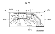
配線基板5は、半導体モジュール2が備える複数の電子部品EDと図示しない実装基板とを電気的に接続するためのインタポーザであって、図4に示すように面5a、面5aの反対側に位置する面5bおよび面5aと面5bの間に位置する側面5cを備えている。また、図2および図3に示すように、面5a、5bはそれぞれ四辺形の平面形状を成し、第1辺5d、第1辺5dと対向する第2辺5e、第1辺5dおよび第2辺の間に位置する第3辺5f、および第3辺5fと対向する第4辺5gを備えている。この第1辺5d、第2辺5e、第3辺5f、第4辺5gは配線基板5の側面5cを構成する。また、配線基板5は、例えば樹脂から成るコア材と、コア材上に形成された複数の配線7を備え、配線基板5に搭載された複数の電子部品EDは、配線7を介して電気的に接続されている。また、複数の電子部品EDは、複数の配線7を介して複数のリード6と電気的に接続されている。
The
本実施の形態では、複数のリード6を配線基板5の一辺に集約して配置している。図2〜図4に示す例では、複数のリード6は、配線基板5の第1辺5dに沿って並べて配置され、第2辺5e、第3辺5f、および第4辺5gにはリード6が、配置されていない。また、複数のリード6は、それぞれ、配線基板5の第1辺5dを跨いで配線基板5の外側に向かって突出するように形成されている。このように複数のリード6を配線基板5の一辺に集約して配置することにより、半導体モジュール2を図示しない実装基板に実装する際には、リード6が配置された配線基板5の側面5cを実装基板の実装面と対向させた状態で実装できる。この結果、配線基板5の面5aまたは面5bが実装基板の実装面と対向するように実装する場合と比較して、半導体モジュール2の実装面積を低減することができる。また、複数のリード6の表面は、実装基板に実装する際の接続材である半田材に覆われているが、リード6を配線基板5の一辺に集約して配置することにより、リード6の表面を容易に半田材で覆うことができる。この点については、後述する半導体モジュール2の製造方法において、詳しく説明する。ただし、半導体モジュール2の実装態様は上記に限定されない。例えば、半導体モジュール2の実装スペースに余裕がある場合には、配線基板5の面5aまたは面5bが実装基板の実装面と対向するように実装することもできる。この場合、配線基板5の四辺のうち、複数の辺に沿ってそれぞれ複数のリード6を配置する構成とすることができる。
In the present embodiment, the plurality of
配線基板5の面5aおよび面5bには、それぞれ電子部品EDが搭載されている。本実施の形態では、面5a側には、パワー半導体デバイスである複数(図2、図3では2個)の半導体装置PAH、PALが搭載されている。一方、面5b側には、パワー半導体デバイス以外の電子部品ED、詳しくは、ドライバ回路が形成された半導体装置PDR、4つの抵抗素子RH1、RH2、RL1、RL2、および一つのダイオード素子D1が搭載されている。言い換えれば、半導体モジュール2は、一方の面5aにパワー半導体デバイスである半導体装置PAH、PALのみが搭載され、その他の電子部品EDは搭載されていない。また他方の面5bには、パワー半導体デバイス以外の電子部品EDが搭載され、パワー半導体デバイスである半導体装置PAH、PALは搭載されていない。半導体装置PAH、PALは、前記したように電源回路に組み込まれるスイッチング素子なので、例えば1A(アンペア)を超える大電流が流れる。このため、半導体装置PAH、PALの周囲に他の電子部品EDを配置すると、電気的影響や熱影響によりノイズが発生し、他の電子部品EDが誤作動する懸念がある。特に、ドライバ回路が形成された半導体装置PDRが誤作動すると、半導体モジュール2のシステムが正しく動作せず、信頼性低下の原因となる。そこで、本実施の形態では、発熱量が相対的に大きいパワー半導体デバイス(半導体装置PAH、PAL)と、その他の電子部品ED(特に、半導体装置PDR)を反対側の面に搭載する。これにより、パワー半導体デバイスと、その他の電子部品EDの間には配線基板5が介在することとなるため、熱影響を低減することができる。この結果、半導体モジュール2の信頼性低下を抑制することができる。
Electronic components ED are mounted on the
図2〜図5に示すように、半導体装置PAH、PALが備える複数のリード6a、6bは、半導体モジュール2のリード6の一部を兼ねている。言い換えれば、半導体モジュール2が備える複数のリード6のうちの一部は、半導体装置PAH、PALと一体に形成されている。半導体装置PAH、PALは、本体部分(リード6以外の部分)が面5a側に配置され、半導体装置PAH、PALがそれぞれ備える複数のリード6a、6bの一部が面5b側に配置されている。詳しくは、配線基板5には、面5aおよび面5bのうち、いずれか一方から他方に向かって貫通する複数の貫通孔SHが形成され、リード6a、6bは、面5a側から面5b側に向かって配線基板5を貫通するように貫通孔SHに挿入される。また、半導体装置PAH、PALが備える複数のリード6a、6bは、貫通孔SH内に埋め込まれた半田(導体膜)SHMにより、貫通孔SHに固定され、これにより、半導体装置PAH、PALは配線基板5に固定されている。このようにリード6a、6bの一部が反対面側に配置される場合であっても、半導体装置PAH、PALが搭載される面は、半導体装置PAH、PALの主たる熱源が搭載される面で定義する。例えば、半導体装置PAH、PALの主たる熱源は、半導体装置PAH、PAL内に封止された半導体チップであるため、本実施の形態では、半導体装置PAH、PALは配線基板5の面5a側に搭載されている。
As shown in FIGS. 2 to 5, the plurality of
また、本実施の形態では、半導体装置PAH、PAL、複数の電子部品EDおよび複数のリード6は、図3に示す配線基板5の面5bに形成された複数の配線7bを介して電気的に接続されている。言い換えれば、半導体装置PAH、PAL、複数の電子部品EDおよび複数のリード6を電気的に接続する配線7は、配線基板5の面5b側に優先的に形成し、面5a側の配線7は最小限に留めている。詳しくは、図3に示すように、配線基板5の面5b側に搭載された複数の電子部品EDと複数のリード6は、面5bに形成された複数の配線7bを介して電気的に接続されている。また、図2に示すように配線基板5の面5a側に搭載された半導体装置PAH、PALが備える複数のリード6a、6bのうち、ハイサイドのスイッチである半導体装置PAHのエミッタ端子Eと、ローサイドのスイッチである半導体装置PALのコレクタ端子Cは、配線基板5の面5aに形成された配線(金属パターン)7aを介して電気的に接続される。そして、面5a側に形成された配線7aは、配線基板5の面5a側の配線層と面5b側の配線層を電気的に接続する層間導電路であるビア(ビア配線)7c(図3参照)により面5b側に引き出され、面5b側の配線7bと電気的に接続されている。また、図3に示すように、半導体装置PAH、PALが備える複数のリード6a、6bのうち、それぞれのゲート端子Gは、配線基板5の面5bにおいて、配線7bを介して電子部品EDと電気的に接続されている。また、半導体装置PALの複数のリード6bのうち、エミッタ端子Eは、配線基板5の面5bにおいて、配線7bを介して半導体装置PDRの端子と電気的に接続されている。
In the present embodiment, the semiconductor devices PAH and PAL, the plurality of electronic components ED, and the plurality of
このように、複数の電子部品EDと複数のリード6を電気的に接続する配線7をパワー半導体デバイス以外の電子部品EDの搭載面である面5b側に優先的に形成することにより、各配線7の線路距離を短くすることができるので、配線7のインピーダンス成分を低減することができる。また、相対的に発熱量が大きいパワー半導体デバイスの搭載面である面5aに形成する配線7aの本数を最小限に留めることにより、パワー半導体デバイスからの熱影響を考慮した放熱設計を容易に行うことができる。この結果、半導体モジュール2の信頼性を向上させることができる。
As described above, the
また、図3に示すように、半導体装置PAH、PALを駆動するドライバ回路が形成された半導体装置PDRは、平面視において、半導体装置PAHと半導体装置PALの間に配置されている。前記したように、半導体装置PAH、PALはそれぞれ、電力変換装置1(図1参照)のハイサイド、ローサイドのスイッチを構成し、半導体装置PDRには各スイッチを駆動するドライバ回路DR1、DR2(図1参照)が形成されている。このため、半導体装置PDRの複数の外部端子のうち、ハイサイド用の出力端子Houtからハイサイド用のゲート端子Gに至る経路(ハイサイド用ゲート線路)と、ローサイド用の出力端子Loutからローサイド用のゲート端子Gに至る経路(ローサイド用ゲート線路)のインピーダンス成分を揃えることが好ましい。つまり、ハイサイド用ゲート線路とローサイド用ゲート線路の線路距離を揃える(等長化する)ことが好ましい。本実施の形態では、ハイサイド用ゲート線路とローサイド用ゲート線路の線路距離はほぼ等しく、ハイサイド用ゲート線路中に直列接続される抵抗素子RH1とローサイド用ゲート線路に直列接続される抵抗素子RL1の抵抗値は、ほぼ等しい。したがって、ハイサイド用ゲート線路とローサイド用ゲート線路のインピーダンス成分は揃っている。 As shown in FIG. 3, the semiconductor device PDR in which the driver circuit for driving the semiconductor devices PAH and PAL is formed is disposed between the semiconductor device PAH and the semiconductor device PAL in plan view. As described above, the semiconductor devices PAH and PAL respectively constitute high-side and low-side switches of the power conversion device 1 (see FIG. 1), and the semiconductor devices PDR have driver circuits DR1 and DR2 (see FIG. 1) is formed. For this reason, among the plurality of external terminals of the semiconductor device PDR, a path (high-side gate line) from the high-side output terminal Hout to the high-side gate terminal G and a low-side output terminal Lout to the low-side use It is preferable that the impedance components of the path (low-side gate line) leading to the gate terminal G of each other are made uniform. That is, it is preferable that the line distances of the high-side gate line and the low-side gate line are equalized (equalized). In the present embodiment, the line distances of the high-side gate line and the low-side gate line are substantially equal, and the resistive element RH1 connected in series in the high-side gate line and the resistive element RL1 connected in series to the low-side gate line. The resistance values of are substantially equal. Therefore, the impedance components of the high-side gate line and the low-side gate line are uniform.
ここで、単に、ハイサイド用ゲート線路とローサイド用ゲート線路の線路距離を揃える観点からは、配線基板5において、配線7を長く引き回せば半導体装置PDRの搭載位置によらず揃えることができる。しかし、ハイサイド用ゲート線路とローサイド用ゲート線路の線路距離が長くなると経路中での損失が増大するので、各ゲート線路の距離は短くすることが好ましい。そこで、図3に示すように、平面視において、半導体装置PAHと半導体装置PALの間に半導体装置PDRを配置することにより、ハイサイド用ゲート線路とローサイド用ゲート線路の線路距離を短くし、かつ、等長化することができる。なお、半導体装置PDRを半導体装置PAHのゲート端子Gと半導体装置PALのゲート端子Gの間に配置して、各ゲート線路を構成する配線7を直線的に配置すれば、ハイサイド用ゲート線路とローサイド用ゲート線路の線路距離を最短にすることができる。しかし、他の電子部品EDや他の配線7のレイアウトとの兼ね合いにより、図3に示すようにゲート線路が多少迂回していても良い。少なくとも、半導体装置PAHと半導体装置PALの間に半導体装置PDRが配置されていれば、各ゲート線路の距離は十分に短くすることができる。また、この場合、電子部品EDの搭載位置や配線7のレイアウトの設計上の自由度が向上する。
Here, simply from the viewpoint of aligning the line distance between the high-side gate line and the low-side gate line, the
また、図3に示すように、半導体モジュール2の複数のリード6のうち、半導体装置PAH、PALが備えるリード6a、6b以外のリード6cは、第1辺5dにおいてリード6a、6bの隣の領域に集約して配置されている。つまり、リード6a、6bとリード6cは混在せず、それぞれ離間した領域に配置されている。このように、半導体装置PAHが備えるリード6a、半導体装置PALが備えるリード6b、およびその他のリード6cを分離した領域に配置することにより、配線7のレイアウトを単純化することができる。これにより、半導体モジュール2全体として、配線7の長さを短くすることができる。
As shown in FIG. 3, among the plurality of
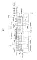
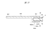
また、本実施の形態では、図4および図5に示すように、半導体装置PAH、PALに放熱板8が固定される。放熱板8は、配線基板5を構成する樹脂よりも熱伝導率が高い金属材料から成る板材であって、例えば本実施の形態ではアルミニウム(Al)から成る。なお、図4および図5では放熱板8を板状の部材として記載したが、半導体装置PAH、PALと対向させる面8aを備えていれば、放熱板8の形状は図4および図5に示す態様に限定されない。例えば、放熱効率を上昇させるため、面8aと異なる位置にフィン(図示は省略)を形成し、放熱面積を増大させることができる。このように、半導体装置PAH、PALに放熱板8を固定することにより、発熱量が相対的に大きいパワー半導体デバイス(半導体装置PAH、PAL)からの熱を効率的に放熱させる。この結果、半導体モジュール2の信頼性を向上させることができる。本実施の形態では、図4および図5に示すように、放熱板8は、ネジ9により半導体装置PAH、PALにネジ止め固定されている。詳しくは、図5に示すように、半導体装置PAH、PALのそれぞれには、半導体装置PAH、PALを厚さ方向に貫通する貫通孔15が形成され、この貫通孔15には、主面PAHa、PALa側からネジ9が挿入されている。そして、主面PAHb、PALb側に配置される放熱板8の面(デバイス対向面)8aには、貫通孔15と重なる位置にネジ穴(側面にネジ9と組み合わせる螺旋状の溝が形成された穴)が形成され、ネジ9をこのネジ穴に挿入し、締め込むことで、放熱板8を半導体装置PAH、PALに固定している。
In the present embodiment, as shown in FIGS. 4 and 5,
以下、放熱板8の固定方法についてさらに詳しく説明する。図5に示すように半導体装置PAH、PALのそれぞれは、互いに反対側に位置する主面を備えている。半導体装置PAHは主面(基材対向面)PAHa、主面PAHaとは反対側に位置する主面(放熱板対向面)PAHbを有している。また、半導体装置PALは、主面(基材対向面)PALa、主面PALaとは反対側に位置する主面(放熱板対向面)PAHbを備えている。ここで、側面視において、配線基板5の面5a側では、半導体装置PALの主面PALbが面5aから最も離れた位置に配置されている。このため、放熱板8の面8aを半導体装置PALの主面PALbと密着させた状態で固定することができる。このように、放熱板8の面8aを半導体装置PALの主面PALbと密着させることで、半導体装置PALからの放熱効率を向上させることができる。
Hereinafter, the fixing method of the
また、半導体装置PAH、PALには、それぞれ半導体装置PAH、PALを厚さ方向に貫通する貫通孔15が形成されている。半導体装置PAHには、主面PAHa、PAHbのうち、いずれか一方から他方まで貫通する貫通孔15aが形成されている。また、半導体装置PALには、主面PALa、PALbのうち、いずれか一方から他方まで貫通する貫通孔15bが形成されている。ここで、図2および図3に示すように、半導体装置PAH、PALのそれぞれは、平面視において、貫通孔15が配線基板5の外側に位置するように面5a(図2参照)に搭載されている。詳しくは、半導体装置PAH、PALのそれぞれは、配線基板5の辺5eから配線基板5の外側に突出するように配置され、突出した領域に貫通孔15が形成されている。言い換えれば、半導体装置PAH,PALのそれぞれは、配線基板5の辺5eを跨ぐように配置され、配線基板5の外側に貫通孔15が形成されている。このように半導体装置PAH、PALの貫通孔15を配線基板5の外側に配置することにより、図5に示すように、ネジ9は配線基板5を介さずに、半導体装置PAH、PALを直接的に固定することができる。
The semiconductor devices PAH and PAL are formed with through
本実施の形態のように、半導体装置PAH、PALに放熱板8をネジ止め固定する方法は、下記の点で好ましい。まず、図4および図5に示す半導体装置PALのように、放熱性低下の原因となる接着層を介さず、主面PALbと放熱板8の面8aを接触させることができるため、放熱性を向上させることができる。また、ネジ9による固定方法は容易に固定することができるため、放熱板8を固定する工程を効率化することができる。また例えば、半導体モジュール2を図示しない実装基板に実装した後でも放熱板8を固定することができるので、放熱板8を固定しない状態で半導体モジュール2を実装基板に実装することができる。また、ネジ9を緩めれば、放熱板8を容易に取り外すことができるので、例えば放熱板8の交換などのメンテナンス作業を容易に行うことができる。
As in the present embodiment, the method of screwing and fixing the
また、本実施の形態のように、複数の半導体装置(パワー半導体デバイス)PAH、PALを備える半導体モジュール2において、一つの放熱板8を固定する場合には、半導体装置PAH、PALのうち、いずれか一方をネジ止め固定し、他方は、ネジ止め固定しない実施態様とすることもできる。しかし、複数の半導体装置PAH、PALのそれぞれに、放熱板8を確実に固定する観点からは、半導体装置PAH、PALのそれぞれに貫通孔15a、15bを形成し、ネジ9a、9bを用いてそれぞれ個別に固定することが好ましい。
Further, in the
<パワー半導体デバイス>
次に、半導体装置PAH、PALの詳細な構造について説明する。図6は、図2〜図5に示すパワー半導体デバイスの内部構造を示す透視平面図、図7は図6のA−A線に沿った断面図である。なお、図2〜図5に示す半導体装置PAH、PALは、同じ構造となっているため、図6および図7を用いて半導体装置PAHおよび半導体装置PALの構造を説明する。
<Power semiconductor devices>
Next, the detailed structure of the semiconductor devices PAH and PAL will be described. 6 is a perspective plan view showing the internal structure of the power semiconductor device shown in FIGS. 2 to 5, and FIG. 7 is a cross-sectional view taken along the line AA of FIG. 2 to 5 have the same structure, the structures of the semiconductor device PAH and the semiconductor device PAL will be described with reference to FIGS.
図7に示すように半導体装置PAHは、主面PAHa、主面PAHaとは反対側に位置する主面PAHb、および主面PAHaと主面PAHbの間に位置する側面PAHcを備えている。主面PAHaは半導体装置PAHの搭載面であり、図5に示すように半導体装置PAHは、主面PAHaが配線基板5の面5aと対向するように配線基板5の面5aに搭載されている。また、半導体装置PALは、主面(基材対向面)PALa、主面PALaとは反対側に位置する主面(放熱板対向面)PALb、および主面PALaと主面PALbの間に位置する側面PALcを備えている。主面PALaは半導体装置PALの搭載面であり、図5に示すように半導体装置PALは、主面PALaが配線基板5の面5aと対向するように配線基板5の面5aに搭載されている。
As shown in FIG. 7, the semiconductor device PAH includes a main surface PAHa, a main surface PAHb positioned on the opposite side of the main surface PAHa, and a side surface PAHc positioned between the main surface PAHa and the main surface PAHb. The main surface PAHa is a mounting surface of the semiconductor device PAH, and the semiconductor device PAH is mounted on the
また、図6に示すように半導体装置PAH、PALのそれぞれは、半導体チップ10と、半導体チップ10を搭載するためのチップ搭載部(タブ、ダイパッド)11と、半導体チップ10と電気的に接続される複数のリード(外部端子)6と、半導体チップ10とリード6を電気的に接続する複数のワイヤ(導電性部材)12と、半導体チップ10および複数のワイヤ12を封止する封止体(樹脂体)13と、を備えている。
As shown in FIG. 6, each of the semiconductor devices PAH and PAL is electrically connected to the
チップ搭載部11は、半導体チップ10の搭載面となる上面11aおよび上面11aの反対側に位置する下面11b、および上面11aと下面11bの間に位置する側面11cを備え、金属から成る板状部材である。本実施の形態では、チップ搭載部11は、例えば銅(Cu)から成る。また、チップ搭載部11は、上面11aおよび側面11cの一部が封止体13に覆われ、封止されている。チップ搭載部11の側面11cの一部を封止体13で覆うことにより、封止体13とチップ搭載部11の接着強度を向上させることができる。
The
一方、チップ搭載部11の下面11bおよび側面11cの他部は、封止体13から露出している。言い換えれば、チップ搭載部11の下面11bは、半導体装置PAH、PALの主面PAHb、PALbの一部を構成し、かつ、主面PAHb、PALbにおいて、封止体13から露出している。このように金属から成るチップ搭載部11の一部を封止体13から露出させることにより、半導体装置PAH、PALの放熱性を向上させることができる。また、チップ搭載部11の下面11bを、半導体装置PAH、PALの主面PAHb、PALbの一部とすることで、放熱板8(図5参照)と、チップ搭載部11bを直接的に接触させることができる。この結果、放熱効率をさらに向上させることができる。
On the other hand, the
また、半導体チップ10は、表面10a、表面10aとは反対側に位置する裏面10b(図7参照)、表面10aに形成される複数(図6では2個)のパッド(表面電極)10c、および裏面10bに形成される裏面電極10d(図7参照)を備えている。図7および図8に示すように、半導体チップ10は裏面10bがチップ搭載部11の上面11aと対向するようにチップ搭載部11に導電性接着材(導電性部材)14を介して搭載される。半導体チップ10には、複数のトランジスタ素子(IGBT)が形成され、各トランジスタ素子を並列に接続している。そして、トランジスタ素子のゲート、およびエミッタは、半導体チップ10の表面10aに形成されたパッド10cに接続されている。つまり、図6に示す2個のパッド10cは、一つがゲート用の電極、もう一つがエミッタ用の電極となっている。一方、トランジスタ素子のコレクタは、半導体チップ10の裏面10bに形成された裏面電極10dに接続されている。
Further, the
また、チップ搭載部11の近傍には、半導体チップ10と電気的に接続される複数のリード(外部端子)6が配置されている。詳しくは、半導体チップ10のゲート用のパッド10cは、ワイヤ12を介してゲート端子Gと電気的に接続されている。また、半導体チップ10のエミッタ用のパッド10cは、ワイヤ12を介してエミッタ端子Eと電気的に接続されている。また、半導体チップ10のコレクタ用の電極である裏面電極10d(図7参照)は、導電性接着材14を介して金属性のチップ搭載部11と接続され、コレクタ端子Cはチップ搭載部11と一体に形成されている。つまり、裏面電極10dは導電性接着材14およびチップ搭載部11を介してコレクタ端子Cと電気的に接続されている。導電性接着材14は、例えば半田材や銀ペースト(多数の銀(Ag)粒子を含むペースト状の樹脂を硬化させて用いる導電性接着材)を用いることができる。このように半導体チップ10の裏面10b側を、導電性接着材14を介してチップ搭載部11と接続すれば、チップ搭載部11を広い放熱経路として活用できるので、放熱性を向上させることができる。また、半導体チップ10のエミッタ電極とコレクタ電極を互いに反対側の面に形成することにより、少ない面積で、多くのトランジスタ素子を形成することができる。言い換えれば、単位面積当たりのトランジスタ素子の集積度を向上させることができる。
A plurality of leads (external terminals) 6 that are electrically connected to the
また、図6に示すように半導体装置PAH、PALの複数のリード6a、6bは、それぞれ封止体13の同じ側面で封止体13の外側に露出し、同じ方向に向かって延びる。詳しくは、半導体装置PAH、PALの封止体13は、第1側面S1、第1側面S1と対向する第2側面S2、第1側面S1と第2側面S2の間に位置する第3側面S3および第3側面S3と対向する第4側面S4を備え、複数のリード6a、6bは、それぞれ第1側面S1から封止体13の外側に突出するように延びる。このように、複数のリード6a、6bを一つの側面S1に沿って集約して配置することで、図2に示すように半導体装置PAH、PALを搭載した半導体モジュール2の複数のリード6を配線基板5の一辺に集約して配置することができる。
As shown in FIG. 6, the plurality of
また、図6に示すように半導体装置PAH、PALを厚さ方向に貫通する貫通孔15aは、チップ搭載部11と重なる位置に形成され、封止体13およびチップ搭載部11を貫通するように形成されている。詳しくは、チップ搭載部11には、貫通孔15よりも開口径が大きい貫通孔11dが形成され、貫通孔15は貫通孔11dの内側に配置されている。このように貫通孔15をチップ搭載部11と重なる位置に形成することにより、ネジ9(図5参照)はチップ搭載部11の貫通孔11dを貫通することとなる。半導体装置PAH、PALに放熱板8(図5参照)をネジ止め固定する際に、特に強い締め付け力が作用する領域は、ネジ9の周辺領域、すなわち、貫通孔15の周辺領域である。したがって、チップ搭載部11をネジ9が貫通することにより、チップ搭載部11の下面11b(図5参照)と放熱板8の面8a(図5参照)を確実に密着させることができる。
Further, as shown in FIG. 6, the through
<複数のパワー半導体デバイスに一枚の放熱板を固定する方法について>
本実施の形態では図5に示すように複数の半導体装置(パワー半導体デバイス)PAH、PALに一つの放熱板8を固定する。そして、半導体装置PAHの主面PAHbおよび半導体装置PALの主面PALbでは、半導体チップ10(図6参照)に電気的に接続されるチップ搭載部11の下面11bが露出している。また、放熱板8は例えばアルミニウムなどの金属から成るため、導電性部材である。このため、半導体装置PAHの主面PAHaと半導体装置PALの主面PALaを一つの放熱板8と直接的に接触させると、半導体装置PAHと半導体装置PALが放熱板8を介して電気的に接続されてしまう。詳しくは、チップ搭載部11は、前記したように、図6に示す半導体チップ10のコレクタ用の電極と電気的に接続されているため、半導体装置PAHのコレクタ端子Cと半導体装置PALのコレクタ端子Cが放熱板8を介して短絡してしまう。
<Method for fixing a single heat sink to a plurality of power semiconductor devices>
In the present embodiment, as shown in FIG. 5, one
そこで、本実施の形態では、複数の半導体装置PAH、PALのコレクタ端子C同士の短絡を防止するため、図5に示すように半導体装置PAH、PALのうちの一方に放熱板8を直接固定し、他方には絶縁シート16を介して放熱板8を固定している。図5に示す例では、2個の半導体装置PAH、PALのうち、半導体装置PALは、チップ搭載部11の下面11bと放熱板8が接触するように固定されている。一方、半導体装置PAHは、チップ搭載部11の下面11bと放熱板8が接触しないように、絶縁シート16を介して固定されている。絶縁シート16は、半導体装置PAHと放熱板8を絶縁するための部材であって、例えば、シート状に成形した樹脂フィルムを用いることができる。ただし、絶縁シート16の絶縁性を阻害しない範囲内で、例えば金属粒子などのフィラー材を添加して、絶縁シート16の熱伝導率を向上させることが好ましい。また、放熱板8は、前記したようにネジ止め固定方式により半導体装置PAHに固定されるので、絶縁シート16には高い接着強度は要求されない。したがって、絶縁シート16の半導体装置PAHの主面PAHbとの対向面、および放熱板8の面8aとの対向面には、粘着層は形成されていない、あるいは、粘着層が形成される場合であってもその厚さは非常に薄い。粘着層を厚く形成すると、絶縁シート16の放熱性を低下させる要因となるが、本実施の形態の絶縁シート16は、粘着層を形成しない、あるいは非常に薄く形成するので放熱性低下を抑制することができる。また、ネジ9を挿入する貫通孔15は、図6および図7に示すようにチップ搭載部11の貫通孔11dの内側に形成され、貫通孔11dと貫通孔15の間は封止体13が配置されている。このため、ネジ9とチップ搭載部11は接触しない構造となっている。したがって、金属性のネジ9を用いた場合であっても、ネジ9を介してチップ搭載部11と放熱板8が短絡することを防止できる。
Therefore, in the present embodiment, in order to prevent a short circuit between the collector terminals C of the plurality of semiconductor devices PAH and PAL, the
また、本実施の形態では半導体装置PAH、PALは同じ構造であるため、厚さ(主面間の距離)も同じである。このため、図5に示すように半導体装置PAHと放熱板8の間に絶縁シート16を配置し、半導体装置PALと放熱板8の間には絶縁シート16を配置しない場合、絶縁シート16の厚さに応じて、主面PAHbと主面PALbの位置をずらさなければ、放熱板8の面8aに、主面PALbと絶縁シート16の面16aを密着させることができない。そこで、本実施の形態では、配線基板5の面5aにおいて、主面PAHbと主面PALbの位置を補正するため、半導体装置PAHと配線基板5の間にスペーサ部材17を配置している。図5に示す例では、半導体装置PALの主面PALaと配線基板5の面5aの間には、スペーサ部材17が配置されている。そして、側面視において、半導体装置PALの主面PALbと、絶縁シート16の放熱板8との面16aの位置は揃っている。このため、半導体装置PALの主面PALbと絶縁シート16の面16aをそれぞれ放熱板8の面8aと密着させることができる。この結果、半導体装置PALからの熱は直接的に、半導体装置PAHからの熱は絶縁シート16を介して、効率的に放熱板8に伝達することができる。なお、主面PALbと対向面16aの位置が揃っているとは、ネジ止め固定方式により、主面PALbと面16aのそれぞれを放熱板8の面8aと密着させることができる程度で同じ高さになっているという意味であり、加工精度等による僅かな位置ずれを排除するものではない。
In the present embodiment, since the semiconductor devices PAH and PAL have the same structure, the thickness (distance between the main surfaces) is also the same. Therefore, when the insulating
スペーサ部材17は、主面PALbと面16aの位置を揃えるための部材であるため、特に構成材料は限定されず、例えば、シート状に形成した樹脂フィルム、あるいは金属板を用いることができる。ただし、半導体装置PALからの熱が、配線基板5の面5b側に伝達されることを抑制する観点からは、絶縁シート16よりも熱伝導率が低い、例えば樹脂フィルムを用いることが好ましい。また、スペーサ部材17は、図5に示すようにネジ止め固定するので、特に接着性は要求されないが、半導体装置PALをより確実に配線基板5に固定して、位置ずれを抑制する観点からは、スペーサ部材17の配線基板5との対向面である面17a、および半導体装置PALとの対向面である面17bにそれぞれ粘着層(接着層)を形成し、スペーサ部材17を介して半導体装置PALを配線基板5に接着固定することが好ましい。また、図示は省略するが、図5に対する変形例として、半導体装置PAHと配線基板5の面5aの間にもスペーサ部材17よりも厚さの薄い(絶縁シート16の厚さ分薄い)スペーサ部材を配置することができる。この場合、半導体装置PAHからの熱が配線基板5の面5b側に伝達されることを抑制することができる。また、半導体装置PAHを図示しないスペーサ部材を介して配線基板5に接着固定すれば、半導体装置PAHの位置ずれを抑制することができる。
Since the
ところで、複数のパワー半導体デバイスのうち、いずれか一方の発熱量が、他方の発熱量よりも高い場合、発熱量が大きい方のパワー半導体デバイスを放熱板8と直接、接続することが好ましい。例えば、図5に示す例では、ローサイド側のスイッチング素子である半導体装置PALは、ハイサイド側のスイッチング素子である半導体装置PAHよりも発熱量が大きい。この場合、相対的に発熱量が大きい半導体装置PALと放熱板8を接触させることにより、半導体モジュール2全体としての放熱効率が向上する。また、相対的に発熱量が大きい半導体装置PALと配線基板5の間にスペーサ部材17を介在させることにより、配線基板5の面5b側への熱影響を低減することができる。
By the way, when the calorific value of any one of the plurality of power semiconductor devices is higher than the calorific value of the other, it is preferable to directly connect the power semiconductor device having the larger calorific value to the
<半導体モジュールの製造方法>
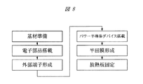
次に、図1〜図7を用いて説明した半導体モジュール2の製造工程について、説明する。図1〜図5に示す半導体モジュール2は、例えば図8に示す組立てフローに沿って製造される。図8は、本実施の形態の半導体モジュールの組立てフローの一例を示す説明図である。
<Semiconductor module manufacturing method>
Next, the manufacturing process of the
1.基材準備工程;
まず、図8に示す基材準備工程では、図9〜図11に示す配線基板5を準備する。図9は、図8に示す基材準備工程で準備する配線基板の一方の面の外観を示す平面図、図10は図9に示す配線基板の反対側の面の外観を示す平面図、図11は図9および図10のD−D線に沿った拡大断面図である。
1. Substrate preparation step;
First, in the base material preparation step shown in FIG. 8, the
本工程で準備する配線基板5は、図11に示すように面5a、面5aの反対側に位置する面5bおよび面5aと面5bの間に位置する側面5c(図9、図10参照)を備えている。また、図9および図10に示すように、面5a、5bはそれぞれ四辺形の平面形状を成し、第1辺5d、第1辺5dと対向する第2辺5e、第1辺5dおよび第2辺の間に位置する第3辺5f、および第3辺5fと対向する第4辺5gを備えている。この第1辺5d、第2辺5e、第3辺5f、第4辺5gは配線基板5の側面5cを構成する。また、図11に示すように、配線基板5は、例えば樹脂から成るコア材20と、コア材20上に形成された複数の配線7を備え、面5aおよび面5bは、それぞれ絶縁膜(ソルダレジスト膜、保護膜)21により覆われている。
As shown in FIG. 11, the
図9に示す面5aには、配線7aが形成され、絶縁膜21に覆われている。また、面5aには、図2に示す半導体モジュール2の外部端子となるリード6(リード6c)を固定するためのパッド22が形成され、パッド22は絶縁膜21から露出している。パッド22は金属膜から成り、例えば配線7aと同じ、銅膜から成る。また、図11に示すように、配線7aは、面5a側の配線層と面5b側の配線層を電気的に接続する層間導電路であるビア(ビア配線)7cと接続され、ビア7cを介して面5b側の配線7bと電気的に接続されている。また、配線基板5には、面5aおよび面5bのうち、いずれか一方から他方に向かって貫通する複数の貫通孔SHを有している。この貫通孔SHは、図2に示す半導体装置PAH、PALのリード6a、6bを挿入するための孔であり、図9の例では、6個の貫通孔SHが設けられている。また、図11に示すように貫通孔SHの内壁には、配線7bと同じ導体膜7dが形成され、導体膜7dは配線7aまたは配線7bと一体に形成されている。つまり、貫通孔SHは、配線基板5の面5a側の配線層と面5b側の配線層を電気的に接続する層間導電路となっている。
A
一方、図10に示す面5bには、複数の配線7bが形成され、絶縁膜21に覆われている。また、面5bには、図2に示す半導体モジュール2の外部端子となるリード6(リード6c)を固定するためのパッド22が形成され、パッド22は絶縁膜21から露出している。面5bの複数のパッド22は、面5aの複数のパッド22の反対側の位置に配置され、図10に示すように面5bにおいて、複数の配線7bと電気的に接続されている。また、面5bには、図2に示す半導体モジュール2の複数の電子部品EDを搭載するための実装端子である複数のランド(パッド、実装端子)23が形成されている。この複数のランド23は配線7bと電気的に接続され、面5b側の絶縁膜21に形成された開口部において、絶縁膜21から露出している。これにより、ランド23に図2に示す電子部品EDの外部端子を接続することができる。なお、図2に示す半導体装置PAH、PALは、複数のリード6a、6bを貫通孔SHに挿入し、半田SHMにより配線基板5と電気的に接続する。したがって、図9および図11に示すように、配線基板5の面5aにはランド23は形成されていない。
On the other hand, a plurality of
ここで、図9および図10に示すように、複数のランド23および複数の貫通孔SHは、配線基板5の四辺のうち、第1辺5dに沿って並べて配置されている。これにより、図2に示す半導体モジュール2のように、複数のリード6を第1辺5dに沿って並べて配置することができる。
Here, as shown in FIGS. 9 and 10, the plurality of
また、図10に示すように、複数のランド23のそれぞれは、複数のパッド22および貫通孔SHよりも第2辺5e側に配置されている。詳しくは、全てのランド23は、全てのパッド22および全ての貫通孔SHよりも第2辺5e側に配置されている。言い換えれば、複数のパッド22のそれぞれは、複数の(全ての)ランド23よりも第1辺5d側に配置される。また、複数の貫通孔SHのそれぞれは、複数の(全ての)ランド23よりも第1辺5d側に配置される。すなわち、複数のランド23は第2辺5e側に、複数の貫通孔SHおよび複数のパッド22は第1辺5d側に、それぞれ集約して配置している。ランド23は、図2に示す半導体モジュール2の面5b側の電子部品EDを搭載するための実装端子である。一方、貫通孔SHは、図2に示す半導体モジュール2の半導体装置PAH、PALのリード6a、6bを電気的に接続するための実装端子、パッド22は、図2に示す半導体モジュールの外部端子であるリード6cを搭載するための実装端子である。したがって、貫通孔SHおよびパッド22を第1辺5d側に、ランド23を第1辺5dとは反対側の第2辺5e側に集約することにより、図2に示す複数のリード6および複数の電子部品EDを、互いに邪魔にならないように配置することができる。また、図8に示す半田膜形成工程では、配線基板5の一部を半田溶液に浸して半田膜を形成するが、半田膜を形成する対象となる外部端子を配線基板5の一辺に集約することで、容易に半田膜を形成することができる。
Further, as shown in FIG. 10, each of the plurality of
2.電子部品搭載工程;
次に、図8に示す電子部品搭載工程では、図12に示すように、配線基板5の面5bに複数の電子部品EDを搭載(実装)する。図12は、図10に示す配線基板上に複数の電子部品を搭載した状態を示す平面図、図13は図11に示す配線基板の上下を反転し、ランド上に電子部品を搭載した状態を示す拡大断面図である。
2. Electronic component mounting process;
Next, in the electronic component mounting step shown in FIG. 8, a plurality of electronic components ED are mounted (mounted) on the
本工程では、図12に示すように、配線基板5の面5bに複数の電子部品EDを搭載し、各電子部品の外部端子24と実装端子であるランド23を電気的に接続する。本工程で搭載する電子部品EDには、半導体装置PAH、PAL(図2参照)を駆動するドライバ回路が形成された半導体装置PDRが含まれる。図12に示す例では、半導体装置PDRの他、4つの抵抗素子RH1、RH2、RL1、RL2および一つのダイオード素子D1を搭載する。以下、半導体装置PDRを例に取り上げて、図13を用いて電子部品EDの搭載方法を説明する。
In this step, as shown in FIG. 12, a plurality of electronic components ED are mounted on the
本工程では、まず、実装端子であるランド23上に接合材25を塗布する。この時、複数のランド23のそれぞれに、接合材25を塗布する。接合材は、例えば半田ペーストなどを用いることができる。次に、被搭載物である半導体装置PDR(電子部品ED)の外部端子24がランド23上に位置するように配置し、接合材25上に置く。そしてリフロー処理として、接合材25を加熱すると、接合材25が外部端子24の表面において濡れ広がり、外部端子24とランド23は、接合材25を介して電気的に接続される。半導体装置PDRは、図13に示すように、半導体チップ26、半導体チップ26を搭載するチップ搭載部(タブ、ダイパッド)27、半導体チップ26の周囲に配置される複数の外部端子(リード)24、半導体チップ26の複数の電極と複数の外部端子24を電気的に接続する複数のワイヤ28、および半導体チップ26と複数のワイヤ28を封止する封止体29を備えている。また、半導体チップ26には、図1に示す2つのドライバ回路(駆動回路)DR1、DR2が形成され、各ドライバ回路は、半導体チップ26の電極に接続されている。したがって、本工程により、半導体チップ26に形成された2つのドライバ回路は、接合材25を介して配線基板5の配線7bと電気的に接続される。また、半導体装置PDR(電子部品ED)は、接合材25を介して配線基板5の面5b上に固定される。
In this step, first, the
ところで、本実施の形態では、複数の電子部品EDを搭載するが、製造効率を向上させる観点からは、複数の電子部品EDを一括して搭載することが好ましい。したがって、本工程では、複数の電子部品EDがそれぞれ備える複数の外部端子24を、接合材25を介してランド23上に置く。そして、例えば、配線基板5を図示しないリフロー炉に搬送し、加熱すれば、配線基板5全体が加熱される。この結果、複数の接合材25が一括して加熱されるため、複数の電子部品EDを一括して配線基板5に搭載することができる。
By the way, in this Embodiment, although the some electronic component ED is mounted, it is preferable to mount the some electronic component ED collectively from a viewpoint of improving manufacturing efficiency. Therefore, in this step, the plurality of
3.外部端子形成工程;
次に、図8に示す外部端子形成工程では、図2に示す半導体モジュール2の外部端子となるリード6cを配線基板5に取り付け、配線基板5と電気的に接続する。図14は、図12に示す外部端子取り付け用のパッドに外部端子を取り付けた状態を示す拡大平面図、図15は図14のF−F線に沿った拡大断面図である。
3. External terminal forming step;
Next, in the external terminal forming step shown in FIG. 8, the
本工程では、図2に示す複数のリード6のうち、半導体装置PAH、PALの外部端子であるリード6a、6b以外のリード6cを形成する。複数のリード6cは、例えば以下のように形成される。
In this step, among the plurality of
まず、図14に示すように、複数のリード6cのそれぞれを配線基板5に形成されたパッド22に取り付ける。図15に示すように、リード6cの一方の端部には、配線基板5を挟んで固定するコネクタ部6c1が形成されている。コネクタ部6c1は、配線基板5の面5aと当接する面6c1a、配線基板5の面5bと当接する面6c1b、および配線基板5の側面5cと当接する面6c1cを備えている。したがって、コネクタ部6c1の面6c1a、と面6c1bの間に設けられた開口部に配線基板5の側面5cを挿入すると、配線基板5は、コネクタ部6c1に挟まれ、リード6cが固定される。また、配線基板5には、予め金属(例えば銅)から成るパッド22が形成されており、パッド22とリード6cが接触することにより、パッド22を介して配線基板5の配線7(図14参照)とリード6cが電気的に接続される。なお、詳細は後述するが、本工程の後、図8に示す半田膜形成工程において、パッド22およびリード6cの表面に半田膜を形成する。これにより、リード6cとパッド22の電気的接続信頼性を向上させることができるので、本工程では、リード6cのコネクタ部6c1と配線基板5のパッド22の位置関係がずれない程度に固定することができれば良い。
First, as shown in FIG. 14, each of the plurality of
また、複数のリード6cのそれぞれは、コネクタ部6c1と一体に形成され、配線基板5の第1辺5dから配線基板5の外側に向かって延びる延在部6c2を備えている。また、各延在部6c2はコネクタ部6c1とは反対側の端部において、複数のリード6cを一体化する連結部6c3により連結されている。このように複数の連結部6c3を介して複数のリード6cが連結された状態で本工程を行うことにより、複数のリード6cのそれぞれを個別に配線基板5に取り付ける場合よりも大幅に製造効率を向上させることができる。なお、連結部6c3は、複数のリード6cを固定した後で、例えばプレス加工により一括して切断することができる。連結部6c3を切断するタイミングは、複数のリード6cを固定した後であれば特に限定されないが、製造工程中の衝撃などによるリード6cの変形を抑制する観点からは、図8に示す半田膜形成工程の後で行うことが好ましい。
Each of the plurality of
また、本工程を実施するタイミングは図8に示す態様には限定されず、変形例として、上記した電子部品搭載工程の前に本工程を行うことができる。すなわち、基材準備工程の後、図12に示す複数の電子部品EDを搭載する前に、図14に示す複数のリード6cを形成することができる。ただし、配線基板5のハンドリング性向上の観点、あるいは、製造工程中の衝撃などによるリード6cの変形を抑制する観点からは、本工程は、電子部品搭載工程の後で行うことが好ましい。
Moreover, the timing which implements this process is not limited to the aspect shown in FIG. 8, As a modification, this process can be performed before the above-mentioned electronic component mounting process. That is, a plurality of
4.パワー半導体デバイス搭載工程;
次に、図8に示すパワー半導体デバイス搭載工程では、図2に示す半導体モジュール2が有するパワー半導体デバイスである半導体装置PAH、PALを配線基板5に取り付ける。図16は、図15に示す配線基板にパワー半導体デバイスを取り付けた状態を示す平面図、図17は、図16に示すH−H線に沿った拡大断面図である。また、図18は、図16に示す配線基板とパワー半導体デバイスを固定した状態で保持する例を示す側面図である。
4). Power semiconductor device mounting process;
Next, in the power semiconductor device mounting step shown in FIG. 8, the semiconductor devices PAH and PAL, which are power semiconductor devices included in the
本工程では、図16および図17に示すように、半導体装置PAH、PALがそれぞれ備える複数のリード6a、6bを配線基板5の貫通孔SHに挿入し、半導体装置PAH、PALを配線基板5の面5b側に配置する。この時、図16に示すように半導体装置PAH、PALは、配線基板5の第2辺5eを跨いで配線基板5の外側に突出するように配置する。また、半導体装置PAH、PALに形成された貫通孔15が、配線基板5の外側に位置するように配置する。一方、半導体装置PAH、PALの封止体13の側面S1から露出する複数のリード6a、6bは、半導体装置PAH、PALよりも第1辺5d側に配置された貫通孔SHを経由して、第1辺5dを跨いで配線基板5の外側に突出するように配置する。第1辺5dは図2に示す半導体モジュール2を実装基板に実装する際に、実装面側の辺となる。したがって、半導体装置PAH、PALの貫通孔15を第1辺5dの反対側に位置する第2辺5eの外側に配置することで、図5に示す放熱板8と実装基板(図示は省略)が互いに邪魔になることを抑制できる。
In this step, as shown in FIGS. 16 and 17, the plurality of
また、前記したように、本実施の形態では、コレクタ端子の短絡を防止するため、図5に示すように半導体装置PAH、PALのうちの一方に放熱板8を直接固定し、他方には絶縁シート16を介して放熱板8を固定する。そして、絶縁シート16の面16aと半導体装置PALの主面PALbの位置を揃えるため、半導体装置PALと配線基板5の間にスペーサ部材17を配置する。したがって、本工程では、相対的に発熱量が大きい半導体装置PALと配線基板5の間には、図17および図18に示すようにスペーサ部材17を配置する。このため、半導体装置PALの主面PALbは、半導体装置PAHの主面PAHbよりもスペーサ部材17の厚さ分、配線基板5の面5bから離れた位置に配置される。
Further, as described above, in this embodiment, in order to prevent a short circuit of the collector terminal, the
また、半導体装置PAH、PALが備える複数のリード6a、6bは、貫通孔SHを経由して、第1辺5dを跨いで配線基板5の外側に突出するように配置するため、封止体13の外側に、少なくとも2箇所の屈曲部を有している。言い換えれば、図17に示すように半導体装置PAH、PALが有する複数のリード6a、6bは、配線基板5の面5b側で形成された屈曲部CV1、および面5a側で形成された屈曲部CV2部をそれぞれ有している。本実施の形態では、半導体装置PAH、PALの製造効率を向上させる観点から、半導体装置PAH、PALを同じ構造としている。また、製造効率向上の観点からこの屈曲部CV1、CV2の位置についても、半導体装置PAH、PALは同様に形成されている。このように同じ構造の半導体装置PAH、PALを異なる高さ(配線基板5の基準面である面5bに対する位置)で配置した場合、図17に示すように配線基板5の面5a側におけるリード6a、6bの高さが異なる高さになる。つまり、半導体装置PALはスペーサ部材17を介して配線基板5に搭載されるため、半導体装置PALの複数のリード6bに形成された屈曲部CV2から配線基板5の面5aまでの距離W2は、半導体装置PAHの複数のリード6aに形成された屈曲部CV2から配線基板5の面5aまでの距離W1よりも短い。
Further, since the plurality of
ところで、図2に示す半導体モジュール2では、半導体装置PAH、PALは、貫通孔SH内に埋め込まれた半田(導体膜)SHMにより配線基板5と電気的に接続され、かつ、配線基板5に固定される。したがって、本工程で、各貫通孔SHに半田SHMを埋め込んで、リフロー処理を施せば、半導体装置PAH、PALを配線基板5に固定することができる。しかし、図8に示す半田膜形成工程において外部端子である複数のリード6の表面に半田膜を形成する際に、各貫通孔SHに半田SHMを埋め込むことができれば、製造効率をさらに向上させることができる。そこで、本実施の形態では、後述する半田膜形成工程で、複数の貫通孔SH内に半田SHMを埋め込む実施態様について説明する。
By the way, in the
後述する半田膜形成工程で半田SHMを埋め込む場合、本工程では、複数のリード6a、6bは、貫通孔SHに挿入されてはいるが、固定はされていない。したがって、後述する半田膜形成工程で、リード6a、6bをしっかりと固定するまでの間は、半導体装置PAH、PALの位置がずれないように仮固定しておくことが好ましい。例えば、半導体装置PALと配線基板5の間にはスペーサ部材17が配置されるので、スペーサ部材17の配線基板5との対向面である面17a、および半導体装置PALとの対向面である面17bにそれぞれ粘着層(接着層)を形成し、スペーサ部材17を介して半導体装置PALを配線基板5に接着固定することができる。一方、半導体装置PAHと配線基板5の間には、スペーサ部材17よりも薄い両面接着テープを配置することで、半導体装置PAHを配線基板5に接着固定することができる。
When the solder SHM is embedded in a solder film forming process described later, in this process, the plurality of
また、半導体装置PAH、PALと配線基板5の接着固定を行わず、半田膜形成工程に搬送する場合には、例えば図18に示す保持治具30のような治具を用いて、半導体装置PAH、PALと配線基板5を挟み、保持した状態で搬送することが好ましい。図18に示す保持治具30は、配線基板5の面5b側に配置される部材31と、面5a側に配置される部材32を有している。部材31は、配線基板5の面5bを押さえる面(基板押さえ面)31aと、面5bとは接触しない窪み部31bを備えている。図18に示すように部材31の窪み部31b内に複数の電子部品EDが位置するように部材31を配置することで、複数の電子部品EDを避けて配線基板5の面5bを押さえる(クランプする)ことができる。一方、部材32は、半導体装置PAHの主面PAHbを押さえる面(デバイス押さえ面)32aと半導体装置PALの主面PALbを押さえる面(デバイス押さえ面)32bを備えている。また、面32aと面32bの間には、それぞれの面の位置(高さ)を補正するための段差部32cが設けられている。この保持治具30で半導体装置PAH、PALと配線基板5を挟みクランプすると、半導体装置PAH、PALを配線基板5の面5aに仮固定することができる。なお、図18に示す保持治具は、本工程で半導体装置PAH、PALを配線基板5に接着固定する場合であっても、搬送治具として用いることができる。
Further, when the semiconductor devices PAH and PAL and the
また、本工程を実施するタイミングは図8に示す態様には限定されず、変形例として、上記した外部端子形成工程または電子部品搭載工程の前に本工程を行うことができる。すなわち、電子部品搭載工程または基材準備工程の後、図14に示す複数のリード6cを取り付ける前に、半導体装置PAH、PALを取り付けることができる。この変形例は、配線基板5のハンドリング性向上の観点、あるいは、製造工程中の衝撃などによるリード6cの変形を抑制する観点からは好ましい。ただし、前記したように、半導体装置PAH、PALを配線基板5に固定せずに、半田膜形成工程に搬送する場合には、半田膜形成工程の直前に、本工程を行うことが好ましい。また、前記した外部端子形成工程での作業中に半導体装置PAH、PALの位置ずれや、リード6a、6bの変形が生じることを抑制する観点からは、本工程は、外部端子形成工程の後で行うことが好ましい。
Moreover, the timing which implements this process is not limited to the aspect shown in FIG. 8, As a modification, this process can be performed before the above-mentioned external terminal formation process or electronic component mounting process. That is, after the electronic component mounting process or the base material preparation process, the semiconductor devices PAH and PAL can be attached before attaching the plurality of
5.半田膜形成工程;
次に、図8に示す半田膜形成工程では、図19および図20に示すように配線基板5に取り付けられた複数のリード6(リード6a、6b、6c)の表面に半田膜(外装めっき膜)SCを形成する。半田膜SCは、図2〜図5に示す半導体モジュール2を図示しない実装基板に実装する際に接合材として用いる半田の濡れ性を向上させるための導体膜である。図19および図20は、図16に示す複数のリードの表面に半田膜を形成する工程を模式的に示す説明図である。
5. Solder film formation process;
Next, in the solder film forming step shown in FIG. 8, a solder film (exterior plating film) is formed on the surface of a plurality of leads 6 (leads 6a, 6b, 6c) attached to the
本工程では、図19および図20に示すように、複数のリード6(リード6a、6b、6c)を半田溶液35に浸漬し、例えば電気めっき法により表面に半田膜SCを形成する。詳しくは、まず、図19に示すように、例えば前記した保持治具30を用いて半導体装置PAH、PALと配線基板5を挟み、保持した状態で半田槽36内に配置された半田溶液35に配線基板5の一部(リード6が形成された第1辺5d側の領域)を浸す。配線基板5の面5aおよび面5bは、前記したようにソルダレジスト膜である絶縁膜21(図11参照)により覆われているため、本工程で配線基板5の一部を半田溶液35に浸すと、半田溶液35に浸され、かつ、絶縁膜21から露出する部分に選択的に半田膜SCを形成することができる。
In this step, as shown in FIGS. 19 and 20, a plurality of leads 6 (leads 6a, 6b, 6c) are immersed in a
ここで、本実施の形態では、前記したように、外部端子である複数のリード6を配線基板の第1辺5d側に集約して配置している。このため、配線基板の第1辺5d側を半田溶液35に浸せば、配線基板の第2辺5e側を浸すこと無く、複数のリード6を半田溶液35に浸すことができる。これにより、全てのリード6の表面に半田膜SCを形成することができる。また、図20に示すように、本工程で複数の貫通孔SHがそれぞれ半田溶液35に浸るようにすることで、複数の貫通孔SHのそれぞれに半田(導体膜)SHMが埋め込まれ、半導体装置PAH、PALはそれぞれ半田SHMにより固定される。また、図20に示すように複数の貫通孔SHは、配線基板5の第1辺5d側に寄せて、第1辺5dに沿って並べて配置されているため、配線基板の第2辺5e側を浸すこと無く、全ての貫通孔SH内に半田SHMを形成することができる。また、図10を用いて説明したように、配線基板5に形成された複数のランド23のそれぞれは、複数のパッド22および貫通孔SHよりも第2辺5e側に配置されている。つまり、図20に示すように配線基板5の面5b側に搭載される複数の電子部品EDの全ては、複数のリード6および複数の貫通孔SHよりも第2辺5e側に配置されている。このため、本工程では、複数の電子部品EDを半田溶液35に浸すこと無く、全てのリード6の表面に半田膜SCを、全ての貫通孔SH内に半田SHMを形成することができる。電子部品ED、およびこれを搭載するための複数のランド23(図10参照)は、前記したように絶縁膜21(図10参照)から露出しているので、これらを半田溶液35に浸すと、表面に半田膜が形成される。そして形成される半田膜の厚さによっては、隣り合う端子間が短絡し、信頼性低下の原因となる。本実施の形態によれば、複数の電子部品EDを半田溶液35に浸すこと無く、全てのリード6の表面に半田膜SCを、全ての貫通孔SH内に半田SHMを形成することができるため、信頼性低下を抑制できる。
Here, in the present embodiment, as described above, the plurality of
また、本実施の形態では、外部端子である複数のリード6の表面に半田膜SCを形成する工程と、複数の貫通孔SH内に半田SHMを形成し、半導体装置PAH、PALを固定する工程を、一括して行う。このため、各工程を個別に行う場合と比較して、工程数を削減できるので、製造効率を向上させることができる。また、本工程では図19に示すように保持治具30を用いて、半導体装置PAH、PALと配線基板5を保持した状態で、半田溶液35に浸漬する。保持治具30は、前記した図18に示すように、配線基板5の面5b側に配置される部材31と、面5a側に配置される部材32を有している。部材31は、配線基板5の面5bを押さえる面(基板押さえ面)31aと、面5bとは接触しない窪み部31bを備えている。図18に示すように部材31の窪み部31b内に複数の電子部品EDが位置するように部材31を配置することで、複数の電子部品EDを避けて配線基板5の面5bを押さえる(クランプする)ことができる。一方、部材32は、半導体装置PAHの主面PAHbを押さえる面(デバイス押さえ面)32aと半導体装置PALの主面PALbを押さえる面(デバイス押さえ面)32bを備えている。また、面32aと面32bの間には、それぞれの面の位置(高さ)を補正するための段差部32cが設けられている。したがって、保持治具30を用いれば、配線基板5の面5b、半導体装置PAHの主面PAHb、半導体装置PALの主面PALbをそれぞれ保持治具30の面31a、32b、32aと密着させた状態で保持できる。つまり、図20に示すように貫通孔SHに半田SHMが形成され、半導体装置PAHPALが配線基板5と固定されるまでの間、所定の位置関係を保つことができる。
Further, in the present embodiment, a step of forming the solder film SC on the surfaces of the plurality of
ただし、前記したように、パワー半導体デバイス搭載工程で半導体装置PAH、PALをそれぞれ配線基板5に接着固定する場合には、例えば、保持治具30を簡易な構造とすることができる。例えば、図18に示す段差部32cを設けず、半導体装置PALの主面PALbと配線基板5の面5bのみを挟んで保持する構造を適用することができる。
However, as described above, when the semiconductor devices PAH and PAL are bonded and fixed to the
6.放熱板固定工程;
次に、図8に示す放熱板固定工程では、図21および図22に示すように半導体装置PAH、PALに放熱板8を取り付け、固定する。図21は、図20に示す半導体モジュールに放熱板を取り付けた状態を示す平面図、図22は、図21に示すJ−J線に沿った拡大断面図である。
6). Heat sink fixing process;
Next, in the heat sink fixing step shown in FIG. 8, the
本工程では、図21および図22に示すように貫通孔15にネジ9を挿入し、放熱板8をネジ止め固定する。図22に示す例では、半導体装置PAH、PALの主面PAHa、PALa側からネジ9を挿入し、貫通孔15を貫通させる。放熱板8の面8a側には、貫通孔15と重なる位置にネジ穴(側面にネジ9と組み合わせる螺旋状の溝が形成された穴)8bが形成され、ネジ9をこのネジ穴8bに挿入し、締め込むことで、放熱板8を半導体装置PAH、PALに固定している。この時、図22に示すように半導体装置PAHと放熱板8の間には、絶縁シート16を配置し、絶縁シート16を介して半導体装置PAHと放熱板8を固定する。これにより、放熱板8として例えばアルミニウム等の金属板を用いた場合でも、半導体装置PAHのチップ搭載部11と半導体装置PALのチップ搭載部11を電気的に分離することができる。また、ネジ9は、チップ搭載部11とは接触しないので、ネジ9を金属とした場合でも、半導体装置PAHのチップ搭載部11と半導体装置PALのチップ搭載部11を電気的に分離することができる。このように、本実施の形態では、ネジ9を用いて半導体装置PAH、PALに放熱板8を固定するので、半導体装置PALの主面PALbと放熱板8を密着させる事ができる。つまり、相対的に発熱量が大きい半導体装置PALの放熱効率を向上させることができるので、半導体モジュール2の信頼性を向上させることができる。
In this step, as shown in FIGS. 21 and 22, a
また、ネジ9による固定方法は、放熱板8を容易に固定することができるので、変形例として半導体モジュール2を実装基板に実装した後で、放熱板8を固定することができる。この場合、図8に示す半田膜形成工程の後、放熱板8を取り付ける前の状態で、外観検査や電気的検査など、必要な検査を行い出荷する。つまり、放熱板8を取り付けるための貫通孔15が形成された状態で半導体モジュール2を出荷することができる。この場合、放熱板8の形状を半導体モジュール2の実装レイアウトに応じて、種々の形状とすることができる。一方、半導体モジュール2は量産することができるため、製造効率を向上させることができる。
Moreover, since the
<変形例>
以上、本発明者によってなされた発明を実施の形態に基づき具体的に説明したが、本発明は前記実施の形態に限定されるものではなく、その要旨を逸脱しない範囲で種々変更可能であることはいうまでもない。
<Modification>
As mentioned above, the invention made by the present inventor has been specifically described based on the embodiment. However, the present invention is not limited to the embodiment, and various modifications can be made without departing from the scope of the invention. Needless to say.
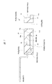
例えば、図1〜図22では、2個のパワー半導体デバイスを備えた半導体モジュールについて説明したが、半導体モジュールが備えるパワー半導体デバイスの数は2個には限定されない。例えば、図23および図24に示すように1個のパワー半導体デバイスを備えた半導体モジュール2Aに適用することができる。図23は、図2に対する変形例である半導体モジュールを示す平面図である。また、図24は図23に示す半導体モジュールに放熱板を固定した状態を示す側面図である。図23および図24に示す半導体モジュール2Aは、パワー半導体デバイスとして、1個の半導体装置PA1のみを備えている点を除き、図1〜図22を用いて説明した半導体モジュール2と同様である。このように1個のパワー半導体デバイスを備えるモジュールとしては、例えば力率改善(整流時の高調波の発生を抑制する)のためのシステムを備えたモジュールなどが例示できる。
For example, in FIGS. 1 to 22, the semiconductor module including two power semiconductor devices has been described, but the number of power semiconductor devices included in the semiconductor module is not limited to two. For example, the present invention can be applied to a
また、図1〜図22では、2個のパワー半導体デバイスの一方は絶縁シートを介して放熱板を固定し、他方は放熱板に接触させた構成について説明したが、半導体モジュールが備えるパワー半導体デバイスの数は2個には限定されず、例えば、2個よりも多いパワー半導体デバイスを備えた半導体モジュールに適用することもできる。例えば、三相モータの駆動回路に組み込まれるインバータでは、6個のパワー半導体デバイスを用いる場合がある。6個のパワー半導体デバイスを備えた半導体モジュールの場合、図1〜図22を用いて説明した半導体モジュール2の構成を3つ横に並べて配置する態様が考えられる。ただし、この場合、外部端子であるリード6が配置される第1辺5dの長さが長くなる。
1 to 22, the configuration in which one of the two power semiconductor devices has a heat sink fixed via an insulating sheet and the other is in contact with the heat sink has been described. The number of is not limited to two, and can be applied to a semiconductor module including more than two power semiconductor devices, for example. For example, an inverter incorporated in a drive circuit of a three-phase motor may use six power semiconductor devices. In the case of a semiconductor module including six power semiconductor devices, a configuration in which three configurations of the
そこで、モジュールの小型化の観点からは、図25に示す半導体モジュール2Bのように、配線基板5の複数の辺にそれぞれ複数のリード(外部端子)6を設け、パワー半導体デバイスをマトリクス状に配置することが好ましい。図25は、図2に対する別の変形例である半導体モジュールを示す平面図である。また、図26は、図25に示す半導体モジュールに放熱板を固定した状態を示す側面図である。図25に示す半導体モジュール2Bは、下記の点で図1〜図22を用いて説明した半導体モジュール2と相違する。まず、半導体モジュール2Bは、6個のパワー半導体デバイスを備えている。詳しくは、3個のハイサイド側の半導体装置PAHと、3個のローサイド側の半導体装置PALを備えている。
Therefore, from the viewpoint of miniaturization of the module, as in the
また、配線基板5の面5aにおける半導体装置PAH、PALのレイアウトは、半導体装置PAHのリード6aが露出する面と、半導体装置PALのリード6bが露出する面が対向するように、それぞれ半導体装置PAHと半導体装置PALを対向させて配置している。また、複数のリード6a、6bは、配線基板5の外側には突出せず、配線基板に形成された配線(図示は省略)を介して半導体装置PDRなど、配線基板5の面5b側に搭載された電子部品ED、および外部端子である複数のリード6と電気的に接続されている。
The layout of the semiconductor devices PAH and PAL on the
また、複数のリード6は、配線基板5の一辺には集約されず、複数の辺に形成されている。図25に示す例では、第1辺5dおよび第1辺と対向する第2辺5eに沿って、それぞれ複数のリード6が配置されている。また、このように複数の辺にリード6を配置するので、半導体モジュール2Bは、面5b側が実装基板(図示は省略)の実装面と対向するように実装する。したがって、複数のリード6は、面5aから面5bに向かう方向に屈曲し、延びている。
The plurality of
また、多数(図25では6個)のパワー半導体デバイスを1個の半導体モジュール2Bに搭載する場合、配線基板5の平面積が大きくなるので、半導体モジュール2Bでは、モジュールの強度を向上させる観点から、各半導体装置PAH、PALを配線基板5から突出させず、配線基板5の面5a内に収まるように配置している。このように、各半導体装置PAH、PALを配線基板5の外側に突出させない実施態様では、半導体モジュール2のように放熱板8をネジ止め固定することが難しい。ネジ止め固定する場合には、配線基板5もネジにより貫通する必要が生じ、製造工程が煩雑になる。また、ネジの締め付け力により、配線基板5に形成された配線が断線する懸念がある。そこで、図25および図26に示す変形例では、3個の半導体装置PALにそれぞれ、絶縁接着シート18を貼り付けて、放熱板8を接着固定している。絶縁接着シート18は、放熱板8との対向面である面18a、および半導体装置PALの主面PALbとの対向面である面18bに粘着層(接着層)が形成されている点を除き前記実施の形態で説明した絶縁シート16(図5参照)と同じである。一方、3個の半導体装置PAHの主面PAHbは、それぞれ放熱板8の面8aと接触させている。つまり、本変形例では、図5を用いて説明したように、スペーサ部材17を一方のパワー半導体デバイスと配線基板5の間に配置して、放熱板8と対向面の位置を揃える技術を適用している。これにより、半導体装置PAHからの熱は、放熱板8に直接伝達されるため、放熱性を向上させることができる。また、本実施の形態では、ハイサイド側の複数の半導体装置PAHと、ローサイド側の複数の半導体装置PALのうちの一方(図26に示す例ではハイサイド側の複数の半導体装置PAH)を放熱板8と接触させている。言い換えれば、2種類の半導体装置PAH、PALのうちの一方は、放熱板8と接触させて、他方は、絶縁接着シート18を介して放熱板8を固定している。この場合、放熱板8に接触するハイサイド側の複数の半導体装置PAHは、それぞれのコレクタ電極が放熱板8を介して電気的に接続されることとなる。しかし、放熱板8に接触するパワー半導体デバイスを同じ種類とすることで、回路の信頼性低下を防止できる。
In addition, when a large number (six in FIG. 25) of power semiconductor devices are mounted on one
ただし、図26に示す例では、放熱板8と半導体装置PAHを接触させるため、放熱板8と半導体装置PAHの間には絶縁接着シート18を配置することができない。このため、放熱板8と半導体装置PAHは直接的には接着固定されない。したがって、放熱板8と半導体装置PAHを安定的に密着させる観点からは、前記した半導体モジュール2のようにネジ止め固定する方式が好ましい。また、絶縁接着シート18と図5に示す絶縁シート16を比較すると、絶縁シート16には高い接着強度が要求されないため、熱伝導率を高くすることができる。したがって、より高い放熱性を確保する観点からは、前記した半導体モジュール2の方が好ましい。
However, in the example shown in FIG. 26, since the
また、上記変形例は、図1〜図22を用いて説明した半導体モジュール2の変形例として説明したが、その要旨を逸脱しない範囲でこれらの構成要素を適宜組み合わせて適用することができる。例えば、図1〜図22を用いて説明した半導体装置PAH、PALのリード6a、6bを配線基板5の外側まで延ばさず、配線基板5に別途、リード6を形成することができる。この場合、半導体装置PAH、PALのリード6a、6bは、貫通孔SHにおいて、配線基板5の配線と電気的に接続され、該配線を介して外部端子である複数のリードと電気的に接続する。このように、半導体装置PAH、PALのリード6a、6bを配線基板5の外側まで延ばさない場合には、リード6a、6bの屈曲部は、それぞれ1箇所で済むので、加工が容易になる。
Moreover, although the said modification was demonstrated as a modification of the
本発明は、半導体モジュールに広く適用可能である。 The present invention is widely applicable to semiconductor modules.
1 電力変換装置
2、2A、2B 半導体モジュール
3 制御回路
5 配線基板(基材)
5a、5b 面
5c 側面
5d 第1辺
5e 第2辺
5f 第3辺
5g 第4辺
6 リード(外部端子)
6a、6b、6c リード
6c1 コネクタ部
6c1a、6c1b、6c1c 面
6c2 延在部
6c3 連結部
7、7a、7b 配線
7c ビア
7d 導体膜
8 放熱板
8a 面
8b ネジ穴
9、9a、9b ネジ
10 半導体チップ
10a 表面
10b 裏面
10c パッド
10d 裏面電極
11 チップ搭載部
11a 上面
11b チップ搭載部
11b 下面
11c 側面
11d 貫通孔
12 ワイヤ(導電性部材)
13 封止体
14 導電性接着材
15、15a、15b 貫通孔
16 絶縁シート
16a 面
17 スペーサ部材
17a、17b 面
18 絶縁接着シート
18a、18b 面
20 コア材
21 絶縁膜
22 パッド
23 ランド
24 外部端子
25 接合材
26 半導体チップ
28 ワイヤ
29 封止体
30 保持治具
31 部材
31a 面
31b 窪み部
32 部材
32a、32b 面
32c 段差部
35 半田溶液
36 半田槽
C コレクタ端子
CV1 屈曲部
CV2 屈曲部
Cin 入力コンデンサ
Cout 出力コンデンサ
D1 ダイオード素子
DR1、DR2 ドライバ回路
E エミッタ端子
ED 電子部品
ET1、ET2 端子
G ゲート端子
GND 基準電位
Hout 出力端子
I1、I2 電流
Iout 出力電流
L コイル
LD 負荷
Lout 出力端子
N 出力ノード
PA1、PAH 半導体装置
PAHa 主面
PAHb 主面
PAHc 側面
PAL 半導体装置
PALa 主面
PALb 主面
PALc 側面
PDR 半導体装置(電子部品)
QH1 パワートランジスタ
QL1 パワートランジスタ
RH1、RH2、RL1、RL2 抵抗素子
S1 第1側面
S2 第2側面
S3 第3側面
S4 第4側面
SC 半田膜
SH 貫通孔
SHM 半田
VIN 入力電源
W1 距離
W2 距離
DESCRIPTION OF
5a,
6a, 6b, 6c Lead 6c1 Connector portion 6c1a, 6c1b, 6c1c Surface 6c2 Extension portion
13
QH1 Power transistor QL1 Power transistors RH1, RH2, RL1, RL2 Resistance element S1 First side surface S2 Second side surface S3 Third side surface S4 Fourth side surface SC Solder film SH Through hole SHM Solder VIN Input power supply W1 Distance W2 Distance
Claims (20)
前記基材に搭載される複数の電子部品と、
前記複数の電子部品と電気的に接続された複数の外部端子と、
を含み、
前記複数の電子部品は、第1主面、前記第1主面とは反対側に位置する第2主面を備え、前記第1主面が前記基材の前記第1面と対向するように前記基材の前記第1面に搭載された第1パワー半導体デバイスと、前記基材の前記第2面に搭載され、かつ、前記第1パワー半導体デバイスを駆動する駆動回路が形成された第1電子部品と、を含み、
側面視において、前記基材の前記第1面側では、前記第1パワー半導体デバイスの前記第2主面が前記第1面から最も離れた位置に配置されており、
前記第1パワー半導体デバイスには、前記第1主面あるいは前記第2主面のうちのいずれか一方から他方まで貫通する第1貫通孔が形成され、
前記第1パワー半導体デバイスは、平面視において、前記第1貫通孔が前記基材の外側に位置するように前記第1面に搭載されていることを特徴とする半導体モジュール。 A base material comprising a first surface, a second surface located on the opposite side of the first surface, and a side surface located between the first surface and the second surface;
A plurality of electronic components mounted on the substrate;
A plurality of external terminals electrically connected to the plurality of electronic components;
Including
The plurality of electronic components include a first main surface and a second main surface located on the opposite side of the first main surface, such that the first main surface faces the first surface of the substrate. A first power semiconductor device mounted on the first surface of the base material and a drive circuit mounted on the second surface of the base material and driving the first power semiconductor device are formed. Including electronic components,
In the side view, on the first surface side of the base material, the second main surface of the first power semiconductor device is disposed at a position farthest from the first surface,
In the first power semiconductor device, a first through hole penetrating from either one of the first main surface or the second main surface to the other is formed,
The semiconductor module, wherein the first power semiconductor device is mounted on the first surface so that the first through hole is located outside the base material in plan view.
前記第1パワー半導体デバイスは、
上面および前記上面の反対側に位置する下面を備え、金属から成るチップ搭載部と、
表面、前記表面とは反対側に位置する裏面、前記表面に形成される複数の表面電極、および前記裏面に形成される裏面電極を備え、前記裏面が前記チップ搭載部の前記上面と対向するように前記チップ搭載部に導電性部材を介して搭載される半導体チップと、
前記半導体チップの前記複数の表面電極および前記裏面電極と電気的に接続される複数のリードと、
前記チップ搭載部の前記上面、前記半導体チップおよび前記導電性部材を封止する封止体と、を備え、
前記チップ搭載部の前記下面は、前記第2主面の一部を構成し、かつ、前記第2主面において、前記封止体から露出しており、
前記第1貫通孔は、前記封止体および前記チップ搭載部を貫通するように形成されていることを特徴とする半導体モジュール。 In claim 1,
The first power semiconductor device includes:
A chip mounting portion made of metal, comprising an upper surface and a lower surface located on the opposite side of the upper surface;
A front surface, a back surface opposite to the front surface, a plurality of front surface electrodes formed on the front surface, and a back electrode formed on the back surface, the back surface facing the top surface of the chip mounting portion A semiconductor chip mounted on the chip mounting portion via a conductive member;
A plurality of leads electrically connected to the plurality of front surface electrodes and the back surface electrode of the semiconductor chip;
A sealing body that seals the upper surface of the chip mounting portion, the semiconductor chip, and the conductive member;
The lower surface of the chip mounting portion constitutes a part of the second main surface, and is exposed from the sealing body on the second main surface,
The first through hole is formed so as to penetrate the sealing body and the chip mounting portion.
前記第1パワー半導体デバイスには、前記第1貫通孔に挿入された第1ネジにより、前記第2主面側に配置された放熱板が固定されることを特徴とする半導体モジュール。 In claim 2,
A semiconductor module, wherein a heat radiating plate disposed on the second main surface side is fixed to the first power semiconductor device by a first screw inserted into the first through hole.
第3主面、前記第3主面とは反対側に位置する第4主面、および前記第3主面、前記第4主面のうち、いずれか一方から他方まで貫通する第2貫通孔を備え、前記第3主面が前記基材の前記第1面と対向し、かつ、平面視において、前記第2貫通孔が前記基材の外側に位置するように前記基材の前記第1面に搭載された第2パワー半導体デバイス、をさらに有し、
前記第1および第2パワー半導体デバイスのそれぞれは、
上面および前記上面とは反対側に位置する下面を備え、金属から成るチップ搭載部と、
表面、前記表面とは反対側に位置する裏面、前記表面に形成される複数の表面電極、および前記裏面に形成される裏面電極を備え、前記裏面が前記チップ搭載部の前記上面と対向するように前記チップ搭載部に導電性部材を介して搭載される半導体チップと、
前記半導体チップの前記複数の表面電極および前記裏面電極と電気的に接続される複数のリードと、
前記チップ搭載部の前記上面、前記半導体チップおよび前記導電性部材を封止する封止体を備え、
前記チップ搭載部の前記下面は、前記第2または第4主面の一部を構成し、かつ、前記第2または第4主面において、前記封止体から露出しており、
前記第1および第2貫通孔のそれぞれは、前記封止体および前記チップ搭載部を貫通するように形成されていることを特徴とする半導体モジュール。 In claim 1,
A third main surface, a fourth main surface located on the opposite side of the third main surface, and a second through hole penetrating from any one of the third main surface and the fourth main surface to the other. The first surface of the substrate so that the third main surface faces the first surface of the substrate and the second through hole is located outside the substrate in plan view. A second power semiconductor device mounted on
Each of the first and second power semiconductor devices includes:
An upper surface and a lower surface located on the opposite side of the upper surface, a chip mounting portion made of metal,
A front surface, a back surface opposite to the front surface, a plurality of front surface electrodes formed on the front surface, and a back electrode formed on the back surface, the back surface facing the top surface of the chip mounting portion A semiconductor chip mounted on the chip mounting portion via a conductive member;
A plurality of leads electrically connected to the plurality of front surface electrodes and the back surface electrode of the semiconductor chip;
A sealing body for sealing the upper surface of the chip mounting portion, the semiconductor chip and the conductive member;
The lower surface of the chip mounting portion constitutes a part of the second or fourth main surface, and is exposed from the sealing body on the second or fourth main surface,
Each of the first and second through holes is formed so as to penetrate the sealing body and the chip mounting portion.
前記第1パワー半導体デバイスは、前記第1貫通孔に挿入された第1ネジにより、前記第2主面側に配置された放熱板に固定され、
前記第2パワー半導体デバイスは、前記第2貫通孔に挿入された第2ネジにより、前記第4主面側に配置された前記放熱板に固定されることを特徴とする半導体モジュール。 In claim 4,
The first power semiconductor device is fixed to a heat sink disposed on the second main surface side by a first screw inserted into the first through hole,
The semiconductor module, wherein the second power semiconductor device is fixed to the heat radiating plate disposed on the fourth main surface side by a second screw inserted into the second through hole.
前記放熱板は金属から成り、
前記第1パワー半導体デバイスは、前記チップ搭載部の前記下面と前記放熱板が接触するように固定され、
前記第2パワー半導体デバイスは、前記チップ搭載部の前記下面と前記放熱板が接触しないように絶縁シートを介して固定されることを特徴とする半導体モジュール。 In claim 5,
The heat sink is made of metal,
The first power semiconductor device is fixed so that the lower surface of the chip mounting portion and the heat sink are in contact with each other.
The second power semiconductor device is fixed through an insulating sheet so that the lower surface of the chip mounting portion and the heat radiating plate do not contact each other.
前記第1パワー半導体デバイスの前記第1主面と前記基材の前記第1面の間には、スペーサ部材が配置され、
側面視において、前記第1パワー半導体デバイスの前記第2主面と、前記絶縁シートのうちの前記放熱板との対向面の位置は揃っていることを特徴とする半導体モジュール。 In claim 6,
A spacer member is disposed between the first main surface of the first power semiconductor device and the first surface of the base material,
In a side view, the position of the opposing surface of the second power surface of the first power semiconductor device and the heat sink of the insulating sheet is aligned.
前記第1および第2パワー半導体デバイスが有する複数のリードは、前記基材の前記第1面側で形成された第1屈曲部、および前記第2面側で形成された第2屈曲部をそれぞれ有し、
前記第1パワー半導体デバイスの前記複数のリードに形成された前記第2屈曲部から前記基材の前記第2面までの第1距離は、前記第2パワー半導体デバイスの前記複数のリードに形成された前記第2屈曲部から前記基材の前記第2面までの第2距離よりも短いことを特徴とする半導体モジュール。 In claim 7,
The plurality of leads of the first and second power semiconductor devices include a first bent portion formed on the first surface side of the base material and a second bent portion formed on the second surface side, respectively. Have
The first distance from the second bent portion formed on the plurality of leads of the first power semiconductor device to the second surface of the base is formed on the plurality of leads of the second power semiconductor device. Further, the semiconductor module is shorter than a second distance from the second bent portion to the second surface of the base material.
前記第1および第2パワー半導体デバイスを含む複数のパワー半導体デバイス以外の前記複数の電子部品は、それぞれ前記基材の前記第2面に搭載され、
前記複数のパワー半導体デバイスのそれぞれが備える複数のリードは、前記基材の前記第1面側から前記第2面側に導出されており、
前記第1電子部品には、前記複数のパワー半導体デバイスを駆動するドライバ回路が形成され、
前記複数のパワー半導体デバイス、前記複数の電子部品および前記複数の外部端子は、前記基材の前記第2面に形成された複数の配線を介して電気的に接続されていることを特徴とする半導体モジュール。 In claim 5,
The plurality of electronic components other than the plurality of power semiconductor devices including the first and second power semiconductor devices are respectively mounted on the second surface of the base material,
The plurality of leads included in each of the plurality of power semiconductor devices are led out from the first surface side of the base material to the second surface side,
A driver circuit that drives the plurality of power semiconductor devices is formed in the first electronic component,
The plurality of power semiconductor devices, the plurality of electronic components, and the plurality of external terminals are electrically connected via a plurality of wirings formed on the second surface of the base material. Semiconductor module.
前記第1および第2パワー半導体デバイス以外の前記複数の電子部品は、それぞれ前記基材の前記第2面に搭載され、
前記第1および第2パワー半導体デバイスのそれぞれが備える複数のリードは、前記基材の前記第1面側から前記第2面側に導出されており、
前記第1電子部品には、前記第1および第2パワー半導体デバイスを駆動するドライバ回路が形成され、
前記複数のパワー半導体デバイス、前記複数の電子部品および前記複数の外部端子は、前記基材の前記第2面に形成された複数の配線を介して電気的に接続され、
前記第1電子部品は、平面視において、前記第1および第2パワー半導体デバイスの間に配置されていることを特徴とする半導体モジュール。 In claim 5,
The plurality of electronic components other than the first and second power semiconductor devices are respectively mounted on the second surface of the base material,
The plurality of leads included in each of the first and second power semiconductor devices are led out from the first surface side of the base material to the second surface side,
In the first electronic component, a driver circuit for driving the first and second power semiconductor devices is formed,
The plurality of power semiconductor devices, the plurality of electronic components, and the plurality of external terminals are electrically connected via a plurality of wirings formed on the second surface of the base material,
The semiconductor module, wherein the first electronic component is disposed between the first and second power semiconductor devices in plan view.
前記基材は第1辺、前記第1辺と対向する第2辺、前記第1辺および前記第2辺と交差する第3辺、および前記第3辺と対向する第4辺を有し、
前記複数の外部端子は、それぞれ前記第1辺に沿って配置され、前記第1および前記第2パワー半導体デバイスは、前記第2辺を跨いで前記基材の外側に突出するように搭載され、
前記複数の電子部品のそれぞれは、前記複数の外部端子よりも前記第2辺側に搭載されていることを特徴とする半導体モジュール。 In claim 5,
The substrate has a first side, a second side facing the first side, a third side intersecting the first side and the second side, and a fourth side facing the third side;
The plurality of external terminals are respectively disposed along the first side, and the first and second power semiconductor devices are mounted so as to protrude outside the base material across the second side,
Each of the plurality of electronic components is mounted closer to the second side than the plurality of external terminals.
前記基材には、前記第1面、前記第2面のうち、いずれか一方から他方まで貫通する複数の貫通孔が形成され、
前記複数の貫通孔には前記第1および第2パワー半導体デバイスの複数のリードが挿入され、かつ、半田材を介して固定され、
前記複数の電子部品のそれぞれは、前記複数の貫通孔よりも前記基材の前記第2辺側に搭載されていることを特徴とする半導体モジュール。 In claim 11,
In the base material, a plurality of through-holes penetrating from any one of the first surface and the second surface to the other are formed,
A plurality of leads of the first and second power semiconductor devices are inserted into the plurality of through holes, and fixed through a solder material;
Each of the plurality of electronic components is mounted on the second side of the base material with respect to the plurality of through holes.
前記第1および第2パワー半導体デバイスは、平面視において、それぞれ前記第2辺を跨ぐように前記基材の外側に突出するように搭載されていることを特徴とする半導体モジュール。 In claim 11,
The first and second power semiconductor devices are mounted so as to protrude outside the base material so as to straddle the second side in plan view.
前記基材に搭載される複数の電子部品と、
前記複数の電子部品と電気的に接続された複数の外部端子と、
を含み、
前記複数の電子部品は、第1主面、前記第1主面とは反対側に位置する第2主面を備え、前記第1主面が前記基材の前記第1面と対向するように前記基材の前記第1面に搭載された第1パワー半導体デバイスと、第3主面、前記第3主面とは反対側に位置する第4主面を備え、前記第3主面が前記基材の前記第1面と対向するように前記基材の前記第1面に搭載された第2パワー半導体デバイスと、前記基材の前記第2面に搭載され、かつ、前記第1および第2パワー半導体デバイスを駆動する駆動回路が形成された第1電子部品と、を含み、
前記第1および第2パワー半導体デバイスのそれぞれは、
上面および前記上面とは反対側に位置する下面を備え、金属から成るチップ搭載部と、
表面、前記表面とは反対側に位置する裏面、前記表面に形成される複数の表面電極、および前記裏面に形成される裏面電極を備え、前記裏面が前記チップ搭載部の前記上面と対向するように前記チップ搭載部に導電性部材を介して搭載される半導体チップと、
前記半導体チップの前記複数の表面電極および前記裏面電極と電気的に接続される複数のリードと、
前記チップ搭載部の前記上面、前記半導体チップおよび前記導電性部材を封止する封止体と、を備え、
前記チップ搭載部の前記下面は、前記第2または第4主面の一部を構成し、かつ、前記第2または第4主面において、前記封止体から露出しており、
前記第1パワー半導体デバイスの前記第2主面側および前記第2パワー半導体デバイスの前記第4主面側には、金属から成る放熱板が配置され、
前記第1パワー半導体デバイスは、前記チップ搭載部の前記下面と前記放熱板が接触するように固定され、
前記第2パワー半導体デバイスは、前記チップ搭載部の前記下面と前記放熱板が接触しないように絶縁シートを介して固定されることを特徴とする半導体モジュール。 A base material comprising a first surface, a second surface located on the opposite side of the first surface, and a side surface located between the first surface and the second surface;
A plurality of electronic components mounted on the substrate;
A plurality of external terminals electrically connected to the plurality of electronic components;
Including
The plurality of electronic components include a first main surface and a second main surface located on the opposite side of the first main surface, such that the first main surface faces the first surface of the substrate. A first power semiconductor device mounted on the first surface of the substrate; a third main surface; a fourth main surface located on the opposite side of the third main surface, wherein the third main surface is the A second power semiconductor device mounted on the first surface of the substrate so as to face the first surface of the substrate; mounted on the second surface of the substrate; and the first and first A first electronic component on which a drive circuit for driving a two-power semiconductor device is formed,
Each of the first and second power semiconductor devices includes:
An upper surface and a lower surface located on the opposite side of the upper surface, a chip mounting portion made of metal,
A front surface, a back surface opposite to the front surface, a plurality of front surface electrodes formed on the front surface, and a back electrode formed on the back surface, the back surface facing the top surface of the chip mounting portion A semiconductor chip mounted on the chip mounting portion via a conductive member;
A plurality of leads electrically connected to the plurality of front surface electrodes and the back surface electrode of the semiconductor chip;
A sealing body that seals the upper surface of the chip mounting portion, the semiconductor chip, and the conductive member;
The lower surface of the chip mounting portion constitutes a part of the second or fourth main surface, and is exposed from the sealing body on the second or fourth main surface,
A heat sink made of metal is disposed on the second main surface side of the first power semiconductor device and the fourth main surface side of the second power semiconductor device,
The first power semiconductor device is fixed so that the lower surface of the chip mounting portion and the heat sink are in contact with each other.
The second power semiconductor device is fixed through an insulating sheet so that the lower surface of the chip mounting portion and the heat radiating plate do not contact each other.
前記第1パワー半導体デバイスの前記第1主面と前記基材の前記第1面の間には、スペーサ部材が配置され、
側面視において、前記第1パワー半導体デバイスの前記第2主面と、前記絶縁シートの前記放熱板との対向面の位置は揃っていることを特徴とする半導体モジュール。 In claim 14,
A spacer member is disposed between the first main surface of the first power semiconductor device and the first surface of the base material,
In a side view, the position of the opposing surface of the second main surface of the first power semiconductor device and the heat sink of the insulating sheet is aligned.
(b)前記基材の前記第2面に複数の電子部品のうちの第1電子部品を搭載する工程、
(c)前記基材に搭載される前記複数の電子部品と電気的に接続される複数の外部端子を前記基材に形成する工程、
(d)前記複数の電子部品のうち、第1主面、前記第1主面とは反対側に位置する第2主面、前記第1主面と前記第2主面の間に配置される半導体チップ、前記半導体チップと電気的に接続される複数のリード、および前記複数のリードのそれぞれ一部が露出するように前記半導体チップを封止する封止体を備える第1パワー半導体デバイスを、前記第1主面が前記基材の前記第1面と対向するように前記基材の前記第1面に搭載する工程、
を含み、
前記第1電子部品には、前記第1パワー半導体デバイスを駆動する駆動回路が形成され、
前記第1パワー半導体デバイスには、前記第1主面、前記第2主面のうち、いずれか一方から他方まで貫通する第1貫通孔が形成され、
前記(d)工程では、
側面視において、前記基材の前記第1面側で、前記第1パワー半導体デバイスの前記第2主面が前記基材の前記第1面から最も離れた位置に配置されるように、かつ、平面視において、前記第1貫通孔が前記基材の外側に位置するように、前記第1パワー半導体デバイスを前記第1面に搭載することを特徴とする半導体モジュールの製造方法。 (A) preparing a substrate comprising a first surface, a second surface located on the opposite side of the first surface, and a side surface located between the first surface and the second surface;
(B) mounting a first electronic component of a plurality of electronic components on the second surface of the base material;
(C) forming a plurality of external terminals electrically connected to the plurality of electronic components mounted on the substrate on the substrate;
(D) Among the plurality of electronic components, the first main surface, the second main surface located on the opposite side of the first main surface, and the first main surface and the second main surface are disposed. A first power semiconductor device comprising: a semiconductor chip; a plurality of leads electrically connected to the semiconductor chip; and a sealing body that seals the semiconductor chip such that a part of each of the plurality of leads is exposed. A step of mounting on the first surface of the substrate such that the first main surface faces the first surface of the substrate;
Including
A driving circuit for driving the first power semiconductor device is formed in the first electronic component,
In the first power semiconductor device, a first through hole penetrating from any one of the first main surface and the second main surface to the other is formed.
In the step (d),
In a side view, on the first surface side of the base material, the second main surface of the first power semiconductor device is disposed at a position farthest from the first surface of the base material, and A method of manufacturing a semiconductor module, comprising mounting the first power semiconductor device on the first surface so that the first through hole is located outside the base material in a plan view.
(e)前記(d)工程の後、前記第1パワー半導体デバイスの前記第1貫通孔に第1ネジを挿入し、前記第1ネジにより前記第2主面側に放熱板を固定する工程、
をさらに含むことを特徴とする半導体モジュールの製造方法。 In claim 16,
(E) After the step (d), a step of inserting a first screw into the first through hole of the first power semiconductor device and fixing a heat sink on the second main surface side by the first screw;
A method for manufacturing a semiconductor module, further comprising:
(e)前記(d)工程の後、前記複数の外部端子の表面に半田膜を形成する工程、
をさらに含み、
前記基材は第1辺、前記第1辺と対向する第2辺、前記第1辺および前記第2辺と交差する第3辺、および前記第3辺と対向する第4辺を有し、
前記複数の外部端子は、それぞれ前記第1辺に沿って配置され、前記第1パワー半導体デバイスは、前記第2辺を跨いで前記基材の外側に突出するように搭載され、
前記複数の電子部品のそれぞれは、前記複数の外部端子よりも前記第2辺側に搭載され、
前記(e)工程では、
前記基材の前記第1辺側を半田溶液に浸し前記複数の外部端子のそれぞれの表面に前記半田膜を形成することを特徴とする半導体モジュールの製造方法。 In claim 16,
(E) a step of forming a solder film on the surface of the plurality of external terminals after the step (d);
Further including
The substrate has a first side, a second side facing the first side, a third side intersecting the first side and the second side, and a fourth side facing the third side;
The plurality of external terminals are respectively disposed along the first side, and the first power semiconductor device is mounted so as to protrude outside the base material across the second side,
Each of the plurality of electronic components is mounted closer to the second side than the plurality of external terminals,
In the step (e),
A method for manufacturing a semiconductor module, comprising: dipping the first side of the base material in a solder solution to form the solder film on the surface of each of the plurality of external terminals.
前記(e)工程では、
前記基材の前記複数の外部端子を前記半田溶液に浸し、かつ、前記複数の電子部品は前記半田溶液に浸さないようにして、前記複数の外部端子のそれぞれの表面に前記半田膜を形成することを特徴とする半導体モジュールの製造方法。 In claim 18,
In the step (e),
The solder film is formed on the surface of each of the plurality of external terminals so that the plurality of external terminals of the base material are immersed in the solder solution, and the plurality of electronic components are not immersed in the solder solution. A method for manufacturing a semiconductor module.
前記基材には、前記第1面、前記第2面のうち、いずれか一方から他方まで貫通する複数の貫通孔が形成され、
前記複数の電子部品のそれぞれは、前記複数の貫通孔よりも前記基材の前記第2辺側に搭載され、
前記(d)工程では、
前記複数の貫通孔に、前記第1パワー半導体デバイスの複数のリードを挿入し、
前記(e)工程では、
前記基材の前記複数の外部端子、および前記複数の貫通孔を前記半田溶液に浸し、かつ、前記複数の電子部品は前記半田溶液に浸さないようにして、前記複数の貫通孔内に半田を埋め込むことを特徴とする半導体モジュールの製造方法。 In claim 19,
In the base material, a plurality of through-holes penetrating from any one of the first surface and the second surface to the other are formed,
Each of the plurality of electronic components is mounted on the second side of the base material from the plurality of through holes,
In the step (d),
Inserting a plurality of leads of the first power semiconductor device into the plurality of through holes,
In the step (e),
The plurality of external terminals of the substrate and the plurality of through holes are immersed in the solder solution, and the plurality of electronic components are not immersed in the solder solution, and solder is inserted into the plurality of through holes. A method of manufacturing a semiconductor module, characterized by being embedded.
Priority Applications (1)
| Application Number | Priority Date | Filing Date | Title |
|---|---|---|---|
| JP2011125141A JP2012253217A (en) | 2011-06-03 | 2011-06-03 | Semiconductor module and method of manufacturing the same |
Applications Claiming Priority (1)
| Application Number | Priority Date | Filing Date | Title |
|---|---|---|---|
| JP2011125141A JP2012253217A (en) | 2011-06-03 | 2011-06-03 | Semiconductor module and method of manufacturing the same |
Publications (1)
| Publication Number | Publication Date |
|---|---|
| JP2012253217A true JP2012253217A (en) | 2012-12-20 |
Family
ID=47525760
Family Applications (1)
| Application Number | Title | Priority Date | Filing Date |
|---|---|---|---|
| JP2011125141A Withdrawn JP2012253217A (en) | 2011-06-03 | 2011-06-03 | Semiconductor module and method of manufacturing the same |
Country Status (1)
| Country | Link |
|---|---|
| JP (1) | JP2012253217A (en) |
Cited By (1)
| Publication number | Priority date | Publication date | Assignee | Title |
|---|---|---|---|---|
| KR20160052602A (en) * | 2013-08-28 | 2016-05-12 | 스마트켐 리미티드 | Polymeric organic semiconductor compositions |
-
2011
- 2011-06-03 JP JP2011125141A patent/JP2012253217A/en not_active Withdrawn
Cited By (2)
| Publication number | Priority date | Publication date | Assignee | Title |
|---|---|---|---|---|
| KR20160052602A (en) * | 2013-08-28 | 2016-05-12 | 스마트켐 리미티드 | Polymeric organic semiconductor compositions |
| KR102091906B1 (en) | 2013-08-28 | 2020-03-20 | 스마트켐 리미티드 | Polymyeric organic semiconductor compositions |
Similar Documents
| Publication | Publication Date | Title |
|---|---|---|
| US9379083B2 (en) | Semiconductor device and method for manufacturing semiconductor device | |
| US7816784B2 (en) | Power quad flat no-lead semiconductor die packages with isolated heat sink for high-voltage, high-power applications, systems using the same, and methods of making the same | |
| US6642576B1 (en) | Power semiconductor device having layered structure of power semiconductor elements and terminal members | |
| WO2013021647A1 (en) | Semiconductor module, semiconductor device provided with semiconductor module, and method for manufacturing semiconductor module | |
| EP2690658B1 (en) | Power semiconductor module and power unit device | |
| KR20150022742A (en) | Semiconductor device | |
| JP2009043820A (en) | High-efficiency module | |
| US7919854B2 (en) | Semiconductor module with two cooling surfaces and method | |
| JP5217884B2 (en) | Semiconductor device | |
| JPWO2007080748A1 (en) | Electric motor drive circuit and air conditioner outdoor unit | |
| JP7088132B2 (en) | Semiconductor devices and electronic devices | |
| JP2009212311A (en) | Electronic device | |
| JP6929813B2 (en) | Power semiconductor device | |
| WO2016067930A1 (en) | Electronic device and method for manufacturing electronic device | |
| US7902464B2 (en) | Heat sink arrangement for electrical apparatus | |
| JP4403166B2 (en) | Power module and power converter | |
| JP6948855B2 (en) | Power semiconductor device and power conversion device using it | |
| JP6892006B2 (en) | Semiconductor device | |
| KR20180087330A (en) | Metal slug for double sided cooling of power module | |
| JP4715283B2 (en) | Power converter and manufacturing method thereof | |
| US20220301998A1 (en) | Power semiconductor module and method for producing a power semiconductor module | |
| JP5188602B2 (en) | Inverter | |
| JP2012253217A (en) | Semiconductor module and method of manufacturing the same | |
| JP5621812B2 (en) | Semiconductor device | |
| WO2022202638A1 (en) | Circuit device |
Legal Events
| Date | Code | Title | Description |
|---|---|---|---|
| A300 | Withdrawal of application because of no request for examination |
Free format text: JAPANESE INTERMEDIATE CODE: A300 Effective date: 20140805 |