JP2012249028A - Transmission device and data transmission method - Google Patents
Transmission device and data transmission method Download PDFInfo
- Publication number
- JP2012249028A JP2012249028A JP2011118491A JP2011118491A JP2012249028A JP 2012249028 A JP2012249028 A JP 2012249028A JP 2011118491 A JP2011118491 A JP 2011118491A JP 2011118491 A JP2011118491 A JP 2011118491A JP 2012249028 A JP2012249028 A JP 2012249028A
- Authority
- JP
- Japan
- Prior art keywords
- frame
- cross
- data
- connect
- client
- Prior art date
- Legal status (The legal status is an assumption and is not a legal conclusion. Google has not performed a legal analysis and makes no representation as to the accuracy of the status listed.)
- Granted
Links
- 230000005540 biological transmission Effects 0.000 title claims abstract description 76
- 238000000034 method Methods 0.000 title claims description 37
- 238000013507 mapping Methods 0.000 claims description 35
- 230000003287 optical effect Effects 0.000 claims description 29
- 238000012545 processing Methods 0.000 description 146
- 238000010586 diagram Methods 0.000 description 32
- 230000001360 synchronised effect Effects 0.000 description 30
- 101100518559 Homo sapiens OTUB1 gene Proteins 0.000 description 15
- 101150115940 OTU1 gene Proteins 0.000 description 15
- 102100040461 Ubiquitin thioesterase OTUB1 Human genes 0.000 description 15
- 238000012500 good manufacturing practice method Methods 0.000 description 8
- 238000000926 separation method Methods 0.000 description 8
- 101100462419 Homo sapiens OTUB2 gene Proteins 0.000 description 3
- 101150046103 OTU2 gene Proteins 0.000 description 3
- 102100025914 Ubiquitin thioesterase OTUB2 Human genes 0.000 description 3
- 238000007796 conventional method Methods 0.000 description 2
- 230000000694 effects Effects 0.000 description 2
- 230000006870 function Effects 0.000 description 2
- 238000009825 accumulation Methods 0.000 description 1
- 238000006243 chemical reaction Methods 0.000 description 1
- 239000000470 constituent Substances 0.000 description 1
- 238000012937 correction Methods 0.000 description 1
- 238000009432 framing Methods 0.000 description 1
- 230000020169 heat generation Effects 0.000 description 1
- 230000010354 integration Effects 0.000 description 1
Images


Classifications
-
- H—ELECTRICITY
- H04—ELECTRIC COMMUNICATION TECHNIQUE
- H04J—MULTIPLEX COMMUNICATION
- H04J3/00—Time-division multiplex systems
- H04J3/16—Time-division multiplex systems in which the time allocation to individual channels within a transmission cycle is variable, e.g. to accommodate varying complexity of signals, to vary number of channels transmitted
- H04J3/1605—Fixed allocated frame structures
- H04J3/1652—Optical Transport Network [OTN]
-
- H—ELECTRICITY
- H04—ELECTRIC COMMUNICATION TECHNIQUE
- H04J—MULTIPLEX COMMUNICATION
- H04J3/00—Time-division multiplex systems
- H04J3/02—Details
- H04J3/06—Synchronising arrangements
- H04J3/0635—Clock or time synchronisation in a network
- H04J3/0685—Clock or time synchronisation in a node; Intranode synchronisation
- H04J3/0691—Synchronisation in a TDM node
-
- H—ELECTRICITY
- H04—ELECTRIC COMMUNICATION TECHNIQUE
- H04L—TRANSMISSION OF DIGITAL INFORMATION, e.g. TELEGRAPHIC COMMUNICATION
- H04L49/00—Packet switching elements
- H04L49/35—Switches specially adapted for specific applications
- H04L49/356—Switches specially adapted for specific applications for storage area networks
- H04L49/357—Fibre channel switches
Abstract
Description
本発明は、伝送装置及びデータ伝送方法に関する。 The present invention relates to a transmission apparatus and a data transmission method.
近年、光伝送システムでは、複数のクライアント装置から入力される非同期のクライアントデータをフレームに変換し、その後、多重して伝送する伝送方式が検討されている。かかる伝送方式としては、例えば、SONET(Synchronous Optical Network)方式、SDH(Synchronous Digital Hierarchy)方式、Ethernet(登録商標)方式、OTN(Optical Transport Network)方式等がある。これらの伝送方式のうち、特に注目されているOTN方式は、SONET方式やSDH方式等のクライアントデータをトランスペアレントに伝送する。 In recent years, in an optical transmission system, a transmission method in which asynchronous client data input from a plurality of client devices is converted into a frame and then multiplexed and transmitted. Examples of such a transmission method include a SONET (Synchronous Optical Network) method, an SDH (Synchronous Digital Hierarchy) method, an Ethernet (registered trademark) method, and an OTN (Optical Transport Network) method. Among these transmission systems, the OTN system, which is particularly attracting attention, transparently transmits client data such as the SONET system and the SDH system.
また、OTN方式では、クライアントデータを多重する場合に、OTNフレーム単位にネットワーク側のTS(Tributary Slot)に配置したり、クライアントデータから複数の下位レイヤのデータへ分離してからネットワーク側のTSに配置したりすることがある。また、OTN方式では、クライアントデータをクライアント装置へそのまま返送することもある。このように、光伝送システムでは、クロスコネクトの機能が要求されている。 In addition, in the OTN system, when client data is multiplexed, it is placed in a TS (Tributary Slot) on the network side in units of OTN frames, or separated from the client data into a plurality of lower layer data and then transferred to the TS on the network side. And may be placed. In the OTN method, client data may be returned to the client device as it is. Thus, the optical transmission system is required to have a cross-connect function.
しかしながら、従来技術では、装置構成が増大するという問題がある。従来技術では、クライアント側において、非同期のクライアントデータを多重する場合に、非同期でクロスコネクトするので、少なくともポート毎にPLL(Phase Locked Loop)回路を利用することがある。かかるPLL回路は、非同期のクライアントデータ同士の干渉によるジッター(Jitter)の蓄積を抑制する用途で利用されることがある。また、従来技術では、ネットワーク側において、フレーム信号を分離する場合に、フレーム単位にクロックを抽出し、非同期でクロスコネクトするので、ポート毎にPLL回路を利用することがある。これらの結果、従来技術では、クライアント側又はネットワーク側において、少なくともポート毎にPLL回路を利用することがあるので、装置構成が増大する。 However, the conventional technique has a problem that the apparatus configuration increases. In the prior art, when asynchronous client data is multiplexed on the client side, asynchronous cross-connection is performed, so a PLL (Phase Locked Loop) circuit may be used at least for each port. Such a PLL circuit may be used for suppressing the accumulation of jitter due to interference between asynchronous client data. In the prior art, when a frame signal is separated on the network side, a clock is extracted for each frame and asynchronously cross-connected, so a PLL circuit may be used for each port. As a result, in the prior art, the PLL circuit is sometimes used at least for each port on the client side or the network side, so that the apparatus configuration increases.
そこで、本願に開示する技術は、上記に鑑みてなされたものであって、装置構成の小型化を図ることが可能である伝送装置及びデータ伝送方法を提供することを目的とする。 Therefore, the technology disclosed in the present application has been made in view of the above, and an object thereof is to provide a transmission device and a data transmission method capable of reducing the size of the device configuration.
上述した課題を解決し、目的を達成するため、本願に開示する伝送装置は、クロックを生成するクロック生成回路と、データを受信する受信器と、前記クロック生成回路によって生成されたクロックを利用して、前記受信器によって受信された非同期な複数のデータをクロスコネクト用のフレームへマッピングするマッピング回路と、前記クロック生成回路によって生成されたクロックを利用して、前記マッピング回路によってマッピングされたクロスコネクト用のフレームをクロスコネクトするクロスコネクトスイッチと、前記クロスコネクトスイッチによってクロスコネクトされたクロスコネクトフレームのデータを送信する送信器とを有する。 In order to solve the above-described problems and achieve the object, a transmission device disclosed in the present application uses a clock generation circuit that generates a clock, a receiver that receives data, and a clock generated by the clock generation circuit. A mapping circuit that maps a plurality of asynchronous data received by the receiver to a cross-connect frame, and a cross-connect mapped by the mapping circuit using a clock generated by the clock generation circuit. A cross-connect switch that cross-connects the frames for use, and a transmitter that transmits data of a cross-connect frame cross-connected by the cross-connect switch.
本願に開示する伝送装置及びデータ伝送方法の一つの様態は、装置構成の小型化を図るという効果を奏する。 One aspect of the transmission device and the data transmission method disclosed in the present application has an effect of reducing the size of the device configuration.
以下に添付図面を参照して、本願に開示する伝送装置及びデータ伝送方法の実施例を説明する。なお、以下の実施例により本発明が限定されるものではない。 Embodiments of a transmission apparatus and a data transmission method disclosed in the present application will be described below with reference to the accompanying drawings. In addition, this invention is not limited by the following examples.
[システム構成]
図1を用いて、本願に開示する伝送装置を含む伝送システムの構成を説明する。図1は、伝送装置を含む伝送システムの構成例を示す図である。
[System configuration]
A configuration of a transmission system including a transmission device disclosed in the present application will be described with reference to FIG. FIG. 1 is a diagram illustrating a configuration example of a transmission system including a transmission apparatus.
例えば、図1に示すように、伝送システムは、例えば、WDM(Wavelength Division Multiplexing)ネットワーク内に伝送装置を有する。また、伝送システムでは、クライアントネットワークを介して、WDMネットワーク内の伝送装置に複数のクライアント装置が接続される。かかるクライアント装置それぞれは、一つの様態として、OC48(STM‐16)、OC3(STM‐1)、1GbE(Giga bit Ethernet(登録商標))、OTU(Optical channel Transport Unit)1等のクライアントデータを伝送装置に入力する。クライアントデータは、クライアント装置それぞれでキャリアが異なり、キャリアごとにクロック源が異なるので、非同期で伝送装置に入力される。 For example, as illustrated in FIG. 1, the transmission system includes a transmission device in a WDM (Wavelength Division Multiplexing) network, for example. In the transmission system, a plurality of client devices are connected to a transmission device in the WDM network via the client network. Each of these client devices, as one form, transmits client data such as OC48 (STM-16), OC3 (STM-1), 1 GbE (Gigabit Ethernet (registered trademark)), OTU (Optical channel Transport Unit) 1, etc. Enter into the device. The client data is input to the transmission device asynchronously because the client device has a different carrier and the carrier has a different clock source.
また、クライアント装置に接続された伝送装置は、例えば、クライアントデータを受け付けて、WDMネットワーク側のDigital Wrapper信号に多重、又はその逆変換である分離を行ない、OTNレイヤでクロスコネクトを行なう。伝送装置は、一つの様態として、光スイッチ装置等の多重分離装置(Muxponder Unit)である。このようにしてWDMネットワークに出力されたデータは、他の伝送装置によって中継され、伝送先のクライアント装置に渡される。なお、伝送装置による処理の詳細については後述する。 The transmission apparatus connected to the client apparatus receives, for example, client data, multiplexes the digital wrapper signal on the WDM network side, or performs separation that is inverse conversion thereof, and performs cross-connect in the OTN layer. The transmission apparatus is, as one aspect, a demultiplexer (Muxponder Unit) such as an optical switch apparatus. The data output to the WDM network in this way is relayed by another transmission apparatus and passed to the transmission destination client apparatus. Details of processing by the transmission apparatus will be described later.
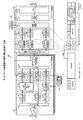
[伝送装置の構成]
次に、図2を用いて、伝送装置の構成を説明する。図2は、実施例1に係る伝送装置の構成例を示す図である。例えば、図2に示すように、伝送装置100は、クロック生成回路101と、同期クロスコネクトスイッチ102と、PLL回路103と、クライアント処理部110と、ネットワーク処理部130とを有する。なお、各クライアントデータに対応する各処理部による処理については後述する。
[Configuration of transmission equipment]
Next, the configuration of the transmission apparatus will be described with reference to FIG. FIG. 2 is a diagram illustrating a configuration example of the transmission apparatus according to the first embodiment. For example, as illustrated in FIG. 2, the
クロック生成回路101は、例えば、クロックを生成する。かかるクロック生成回路101は、一つの様態として、ネットワーク処理部130における送信クロックであっても良い。クロック生成回路101によって生成されたクロックは、クライアント処理部110又はネットワーク処理部130の所定の処理部によって利用される。同期クロスコネクトスイッチ102は、例えば、クライアント処理部110から受け付けたクライアントデータをネットワーク処理部130側へ入力したり、クライアント処理部110側へ返送したりする。また、同期クロスコネクトスイッチ102は、例えば、ネットワーク処理部130から受け付けたネットワークデータをクライアント処理部110へ入力したり、ネットワーク処理部130側へ返送したりする。また、同期クロスコネクトスイッチ102は、クロック生成回路101によって生成されたクロックを利用して、クロスコネクト処理を実行する。PLL回路103は、例えば、クライアント装置それぞれに対して、ODU(Optical channel Data Unit)k(k=0,1)フレームから非同期なクライアントデータそれぞれを送信するために利用される。
The
クライアント処理部110は、例えば、クロック生成回路101によって生成されたクロックを利用して、非同期なクライアントデータをクライアントデータ毎にクロスコネクト用のフレームへマッピングする。また、クライアント処理部110は、クライアント装置の数と同数配設される。また、クライアント処理部110は、光モジュール111と、セレクタ部112と、符号化部113と、フレーム生成回路114と、フレーム生成回路115と、フレーム終端回路116と、フレーム生成回路117とを有する。また、クライアント処理部110は、フレーム終端回路118と、分離/多重回路(Mux/DMux)119と、フレーム終端回路120と、フレーム終端回路121と、セレクタ部122と、クロスコネクトフレーム生成回路123とを有する。なお、図2に示す破線で囲われたフレーム生成回路115、フレーム生成回路117、フレーム終端回路120、フレーム終端回路121は、それぞれ、クロック生成回路101によって生成されたクロックを利用することを表している。また、図2に示す破線で囲われたフレーム生成回路114と、分離/多重回路119とは、PLL回路103が利用される処理部であることを表している。
For example, the
光モジュール111は、例えば、クライアントネットワークを介してクライアント装置からクライアントデータを受信し、光信号から電気信号に変換する。セレクタ部112は、例えば、光モジュール111によって電気信号に変換されたクライアントデータの種別によって、符号化部113、フレーム終端回路116、或いはフレーム終端回路118にクライアントデータを出力する。
For example, the optical module 111 receives client data from a client device via a client network, and converts the optical signal into an electrical signal. The
符号化部113は、例えば、IEEE(Institute of Electrical and Electronics Engineers)802.3で規格化されたGbEフレーム処理と8B10B符号化処理を実行する。フレーム生成回路114は、例えば、ITU‐T(International Telecommunication Union‐Telecommunication standardization sector)勧告G.709及びG.7041で規格化されたGFP(Generic Framing Procedure)‐Tフレームを処理する。フレーム生成回路115は、例えば、GFP‐TフレームからODUk(k=0)フレームにマッピングする。このとき、フレーム生成回路115は、GFP‐TフレームからODUk(k=0)フレームにマッピングする場合に、クロック生成回路101によって生成されたクロックに同期して処理する。すなわち、符号化部113と、フレーム生成回路114とは、クライアントのキャリアごとに異なるクロックにより従属同期して処理し、フレーム生成回路115は、クロック生成回路101によって生成されたクロックに同期して処理する。
For example, the
フレーム終端回路116は、例えば、OCx(x=3,12,48等)信号を終端する。フレーム生成回路117は、例えば、ITU‐T勧告のG.709で規格された処理で、OCx(x=3,12,48等)フレームからODUk(k=0)フレームにマッピングする。このとき、フレーム生成回路117は、OCx(x=3,12,48等)フレームからODUk(k=0)フレームにマッピングする場合に、クロック生成回路101によって生成されたクロックに同期して処理する。すなわち、フレーム終端回路116は、クライアントのキャリアごとに異なるクロックにより従属同期して処理し、フレーム生成回路117は、クロック生成回路101によって生成されたクロックに同期して処理する。
The
フレーム終端回路118は、例えば、OTU1信号を終端する。また、フレーム終端回路118からセレクタ部122へのパスにおいて、フレーム終端回路118は、ITU‐T勧告のG.709で規格された処理で、FEC(Forward Error Correction)符号をデコードし、ODUk(k=1)信号に変換する。すなわち、フレーム終端回路118は、クライアントのキャリアごとに異なるクロックにより従属同期して処理する。
The
分離/多重回路119は、例えば、ODUk(k=1)フレームから下位レイヤの2本のODUk(k=0)フレームを分離する。フレーム終端回路120とフレーム終端回路121とは、ODUk(k=0)信号を終端する。このとき、フレーム終端回路120とフレーム終端回路121とは、クロック生成回路101によって生成されたクロックに同期して処理する。すなわち、フレーム終端回路118と、分離/多重回路119とは、クライアントのキャリアごとに異なるクロックにより従属同期して処理し、フレーム終端回路120と、フレーム終端回路121とは、クロック生成回路101によって生成されたクロックに同期して処理する。
For example, the demultiplexing /
セレクタ部122は、例えば、フレーム生成回路115、フレーム生成回路117、フレーム終端回路118、フレーム終端回路120、フレーム終端回路121によって入力されたデータをクロスコネクトフレーム生成回路123に出力する。また、セレクタ部122は、例えば、ネットワーク処理部130側から入力されたデータを、クライアントデータの種別によって、フレーム生成回路115、フレーム生成回路117、フレーム終端回路118、フレーム終端回路120、フレーム終端回路121に出力する。クロスコネクトフレーム生成回路123は、例えば、フレームそれぞれについて、クロスコネクトフレームにマッピングする。このとき、クロスコネクトフレーム生成回路123は、クロック生成回路101によって生成されたクロックに同期して処理し、クロスコネクトフレームを構成する。
For example, the
ネットワーク処理部130は、例えば、同期クロスコネクトスイッチ102からデータを受け付けた場合に、クロック生成回路101によって生成されたクロックを利用して、ネットワークへのデータ伝送に係る各種処理を実行する。また、ネットワーク処理部130は、例えば、ネットワークからデータを受信した場合に、ネットワークデータから複数の非同期フレームへ分離し、分離したフレームをクロスコネクト用のフレームへマッピングする。また、ネットワーク処理部130は、クロスコネクトフレーム終端回路131a〜131hと、フレーム終端回路132a〜132hと、分離/多重回路133と、フレーム生成回路134と、光モジュール135とを有する。なお、図2に示す破線で囲われたフレーム終端回路132a〜132hは、クロック生成回路101によって生成されたクロックを利用することを表している。また、図2に示す破線で囲われたクロスコネクトフレーム終端回路131a〜131hは、同様に、クロック生成回路101によって生成されたクロックを利用することを表している。
For example, when receiving data from the synchronous
クロスコネクトフレーム終端回路131a〜131hは、例えば、同期クロスコネクトスイッチ102から入力されたクロスコネクトフレーム信号を終端する。フレーム終端回路132a〜132hは、クロスコネクトフレーム信号からODUk(k=0,1)フレームへ分離する。分離/多重回路133は、例えば、分離されたODUk(k=0,1)フレーム信号をODUk(k=2)フレームに多重する。フレーム生成回路134は、例えば、ODUk(k=2)フレームからOTU2フレームにマッピングする。光モジュール135は、例えば、電気信号を光信号に変換してWDMネットワークに出力する。また、ネットワークデータを受け付けた場合には、分離/多重回路133によってフレーム終端回路132a〜132hに分離されたデータが、クロスコネクトフレーム終端回路131a〜131hにおいてクロスコネクトフレームにマッピングされる。なお、ネットワーク処理部130に含まれる各処理部は、クロック生成回路101によって生成されたクロックを利用して処理する。
For example, the cross-connect
[フレームマッピング]
次に、図3A及び図3Bを用いて、フレームマッピングの構成を説明する。図3Aは、従来技術に係るフレームマッピングの構成例を示す図であり、図3Bは、実施例1に係るクロスコネクト同期化時のフレームマッピングの構成例を示す図である。
[Frame mapping]
Next, the configuration of frame mapping will be described with reference to FIGS. 3A and 3B. FIG. 3A is a diagram illustrating a configuration example of frame mapping according to the related art, and FIG. 3B is a diagram illustrating a configuration example of frame mapping at the time of cross-connect synchronization according to the first embodiment.
図3A及び図3Bに示すクライアント側の「Opt.#1〜Opt.#8」は、クライアント装置それぞれから、光モジュール111にクライアントデータが入力されるポートのイメージを表している。また、同様に、ネットワーク側の「Opt.」は、WDMネットワークへデータ出力されるポートのイメージを表している。また、同様に、「OC3」、「OC12」、「OC48」、「STMxx」、「1GE」、「OUT1」、「OUT1」は、クライアント装置それぞれから入力されるクライアントデータの種別を表している。また、同様に、「ODU0」、「ODU1」、「ODUk」等は、フレームを表している。また、同様に、「1.25G TS#1」〜「1.25G TS#8」は、フレーム終端回路132a〜132hを表している。また、同様に、「ODU2」、「OTU2」は、それぞれ、分離/多重回路133、フレーム生成回路134を表している。また、図3Bに示すクライアント側「SWINF(switch interface)」は、クロスコネクトフレーム生成回路123を表している。また、同様に、ネットワーク側「SWINF」は、クロスコネクトフレーム終端回路131a〜131hを表している。要するに、図3Bに示すように、伝送装置100は、ネットワーク側のODUkと、クライアント側のODUkとの間にSWINFを設けることにより、クライアント側のSWINF以降のデータについて、同期化したクロスコネクトを行なう。
“
[クライアントデータがGbEのときの動作]
次に、図4を用いて、クライアントデータがGbEのときのクライアント処理部110の動作を説明する。図4は、クライアントデータがGbEのときのクライアント処理部110の動作例を説明する図である。なお、図4において、クライアントデータがGbEのときに利用されない処理部については斜線を付している。
[Operation when client data is GbE]
Next, the operation of the
例えば、図4に示すように、符号化部113は、IEEE802.3で規格化されたGbEフレーム処理と8B10B符号化処理を実行し、フレーム生成回路114は、ITU‐T勧告G.709及びG.7041で規格化されたGFP‐Tフレームを処理する。ここで、クライアントデータは、光モジュール111、セレクタ部112、符号化部113、フレーム生成回路114、フレーム生成回路115、セレクタ部122、クロスコネクトフレーム生成回路123の順に各処理部において処理される。その後、クライアントデータは、同期クロスコネクトスイッチ102を介して、ネットワーク処理部130へ伝送される。一方、ネットワーク側からのデータは、ネットワーク処理部130、同期クロスコネクトスイッチ102を介して、クライアント処理部110へ伝送される。
For example, as shown in FIG. 4, the
詳細には、図4の下方に示すように、フレーム生成回路114からフレーム生成回路115において、GFP‐TフレームからODUk(k=0)フレームにマッピングされる場合には、クロック生成回路101によって生成されたクロックが利用される。このとき、ITU‐T勧告G.709で規格化されたGMP(Generic Mapping Procedure)方式を使用するため、GFP‐TフレームとODUk(k=0)フレームとの間で周波数偏差が発生したとしても、データを欠落させることなく伝送できる。すなわち、OPU(Optical channel Payload Unit)k(k=0)フレーム内に配置されるJC(justification)バイト及びStuffバイトで周波数偏差が吸収されるため、データを欠落させることなく伝送できる。
Specifically, as shown in the lower part of FIG. 4, when the
また、フレーム生成回路115、セレクタ部122、クロスコネクトフレーム生成回路123において、ODUk(k=0)フレームからクロスコネクトフレームにマッピングされる場合には、クロック生成回路101によって生成されたクロックが利用される。このとき、クロスコネクトフレームへのマッピングにGMP方式を使用するため、ODUk(k=0)フレームとクロスコネクトフレームとの間で周波数偏差が発生したとしても、データを欠落させることなく伝送できる。すなわち、クロスコネクトフレーム内に配置されるJCバイト及びStuffバイトで周波数偏差が吸収されるため、データを欠落させることなく伝送できる。
When the
図5は、クライアントデータがGbEのときのクロスコネクトフレームの例を示す図である。例えば、図5に示すように、ODUk(k=0)の1フレームのみをクロスコネクトフレームにマッピングする場合には、Payloadを2TS(Tributary Slot)構成とし、このうちの1TSを使用してマッピングが行なわれる。なお、図5において、斜線部分は、Stuffバイトを示している。 FIG. 5 is a diagram illustrating an example of a cross-connect frame when the client data is GbE. For example, as shown in FIG. 5, when only one frame of ODUk (k = 0) is mapped to a cross-connect frame, Payload has a 2TS (Tributary Slot) configuration, and mapping is performed using one of these TSs. Done. In FIG. 5, the shaded portion indicates the stuff byte.
つまり、図4に示すクライアント処理部110によれば、クロスコネクトフレームのビットレートをODUk(k=1)フレームよりも早い周波数で、且つ、ODUk(k=0,1)フレームの帯域を確保できる周波数としている。この結果、マッピングするODUk(k=0,1)フレームを欠落することなく、ネットワーク処理部130においても利用されるクロックに同期したクロスコネクトフレームを構成することができる。
That is, according to the
[クライアントデータがOC3/OC12のときの動作]
次に、図6を用いて、クライアントデータがOC3/OC12のときのクライアント処理部110の動作を説明する。図6は、クライアントデータがOC3/OC12のときのクライアント処理部110の動作例を説明する図である。なお、図6において、クライアントデータがOC3/OC12のときに利用されない処理部については斜線を付している。
[Operation when client data is OC3 / OC12]
Next, the operation of the
例えば、図6に示すように、クライアントデータは、光モジュール111、セレクタ部112、フレーム終端回路116、フレーム生成回路117、セレクタ部122、クロスコネクトフレーム生成回路123の順に各処理部において処理される。その後、クライアントデータは、同期クロスコネクトスイッチ102を介して、ネットワーク処理130へ伝送される。一方、ネットワーク側からのデータは、ネットワーク処理部130、同期クロスコネクトスイッチ102を介して、クライアント処理部110へ伝送される。
For example, as shown in FIG. 6, the client data is processed in each processing unit in the order of the optical module 111, the
詳細には、図6の下方に示すように、フレーム終端回路116からフレーム生成回路117において、OC3/OC12信号からODUk(k=0)フレーム信号へマッピングされる場合には、クロック生成回路101によって生成されたクロックが利用される。このとき、ITU‐T勧告のG.709で規格化されたGMP方式を使用するため、OC3/OC12フレームとODUk(k=0)フレームとの間で周波数偏差が発生したとしても、データを欠落することなく伝送できる。すなわち、OPUk(k=0)フレーム内に配置されるJCバイト及びStuffバイトで周波数偏差が吸収されるため、データを欠落させることなく伝送できる。
Specifically, as shown in the lower part of FIG. 6, when mapping from the OC3 / OC12 signal to the ODUk (k = 0) frame signal is performed by the
また、フレーム生成回路117、セレクタ部122、クロスコネクトフレーム生成回路123において、ODUk(k=0)フレームからクロスコネクトフレームにマッピングされる場合には、クロック生成回路101によって生成されたクロックが利用される。このとき、クロスコネクトフレームへのマッピングにGMP方式を使用するため、ODUk(k=0)フレームとクロスコネクトフレームとの間で周波数偏差が発生したとしても、データを欠落させることなく伝送できる。すなわち、クロスコネクトフレーム内に配置されるJCバイト及びStuffバイトで周波数偏差が吸収されるため、データを欠落させることなく伝送できる。
When the
図7は、クライアントデータがOC3/OC12のときのクロスコネクトフレームの例を示す図である。例えば、図7に示すように、ODUk(k=0)の1フレームのみをクロスコネクトフレームにマッピングする場合には、Payloadを2TS構成とし、このうちの1TSを使用してマッピングが行なわれる。なお、図7において、斜線部分は、Stuffバイトを示している。 FIG. 7 is a diagram illustrating an example of a cross-connect frame when the client data is OC3 / OC12. For example, as shown in FIG. 7, when only one frame of ODUk (k = 0) is mapped to the cross-connect frame, Payload has a 2TS configuration, and mapping is performed using one of these TSs. In FIG. 7, the shaded portion indicates the stuff byte.
つまり、図6に示すクライアント処理部110によれば、クロスコネクトフレームのビットレートをODUk(k=1)フレームより早い周波数で、且つ、ODUk(k=0,1)フレームの帯域を確保できる周波数としている。この結果、マッピングするODUk(k=0,1)フレームを欠落することなく、ネットワーク処理部130においても利用されるクロックに同期したクロスコネクトフレームを構成することができる。
That is, according to the
[クライアントデータがOC48のときの動作]
次に、図8を用いて、クライアントデータがOC48のときのクライアント処理部110の動作を説明する。図8は、クライアントデータがOC48のときのクライアント処理部110の動作例を説明する図である。なお、図8において、クライアントデータがOC48のときに利用されない処理部については斜線を付している。
[Operation when client data is OC48]
Next, the operation of the
例えば、図8に示すように、クライアントデータは、光モジュール111、セレクタ部112、フレーム終端回路116、フレーム生成回路117、セレクタ部122、クロスコネクトフレーム生成回路123の順に各処理部において処理される。その後、クライアントデータは、同期クロスコネクトスイッチ102を介して、ネットワーク処理部130へ伝送される。一方、ネットワーク側からのデータは、ネットワーク処理部130、同期クロスコネクトスイッチ102を介して、クライアント処理部110へ伝送される。
For example, as shown in FIG. 8, the client data is processed in each processing unit in the order of the optical module 111, the
詳細には、図8の下方に示すように、フレーム終端回路116からフレーム生成回路117において、OC48信号からODUk(k=1)フレーム信号へマッピングされる場合には、クロック生成回路101によって生成されたクロックが利用される。このとき、ITU‐T勧告のG.709で規格化されたBMP(Bit synchronous Mapping Procedure)方式を使用するため、OC48フレームとODUk(k=1)フレームとの間で周波数偏差が発生したとしても、データを欠落することなく伝送できる。すなわち、OC48よりもODUk(k=1)フレームの周波数の方が早いため、OC48フレームの帯域を確保して、データを欠落させることなくODUk(k=1)フレームを生成することができる。
Specifically, as shown in the lower part of FIG. 8, when the OC48 signal is mapped to the ODUk (k = 1) frame signal in the
また、フレーム生成回路117、セレクタ部122、クロスコネクトフレーム生成回路123において、ODUk(k=1)フレームからクロスコネクトフレームにマッピングされる場合には、クロック生成回路101によって生成されたクロックが利用される。このとき、クロスコネクトフレームへのマッピングにGMP方式を使用するため、ODUk(k=1)フレームとクロスコネクトフレームとの間で周波数偏差が発生したとしても、データを欠落することなく伝送できる。すなわち、クロスコネクトフレーム内に配置されるJCバイト及びStuffバイトで周波数偏差が吸収されるため、データを欠落させることなく伝送できる。
When the
図9は、クライアントデータがOC48のときのクロスコネクトフレームの例を示す図である。例えば、図9に示すように、ODUk(k=1)フレームをクロスコネクトフレームにマッピングする場合には、Payloadを2TS構成とし、この2TSの両方を使用してマッピングが行なわれる。なお、図9において、斜線部分は、Stuffバイトを示している。 FIG. 9 is a diagram illustrating an example of a cross-connect frame when the client data is OC48. For example, as shown in FIG. 9, when an ODUk (k = 1) frame is mapped to a cross-connect frame, Payload has a 2TS configuration, and mapping is performed using both of these 2TSs. In FIG. 9, the shaded area indicates the stuff byte.
つまり、図8に示すクライアント処理部110によれば、クロスコネクトフレームのビットレートをODUk(k=1)フレームより早い周波数で、且つ、ODUk(k=0,1)フレームの帯域を確保できる周波数としている。この結果、マッピングするODUk(k=0,1)フレームを欠落することなく、ネットワーク処理部130においても利用されるクロックに同期したクロスコネクトフレームを構成することができる。
That is, according to the
[クライアントデータがOTU1で下位レイヤへ分離しないときの動作]
次に、図10を用いて、クライアントデータがOTU1で下位レイヤへの分離を行なわないときのクライアント処理部110の動作を説明する。図10は、クライアントデータがOTU1で下位レイヤへの分離を行なわないときのクライアント処理部110の動作例を説明する図である。なお、図10において、クライアントデータがOTU1で下位レイヤへ分離しないときに利用されない処理部については斜線を付している。
[Operation when client data is not separated into lower layer in OTU1]
Next, the operation of the
例えば、図10に示すように、クライアントデータは、光モジュール111、セレクタ部112、フレーム終端回路118、セレクタ部122、クロスコネクトフレーム生成回路123の順に各処理部において処理される。その後、クライアントデータは、同期クロスコネクトスイッチ102を介して、ネットワーク処理部130へ伝送される。一方、ネットワーク側からのデータは、ネットワーク処理部130、同期クロスコネクトスイッチ102を介して、クライアント処理部110へ伝送される。
For example, as shown in FIG. 10, the client data is processed in each processing unit in the order of the optical module 111, the
詳細には、図10の下方に示すように、フレーム終端回路118からセレクタ部122において、ODUk(k=1)フレームからクロスコネクトフレームにマッピングされる。このとき、クロスコネクトフレームへのマッピングにGMP方式を使用するため、ODUk(k=1)フレームとクロスコネクトフレームとの間で周波数偏差が発生したとしても、データを欠落することなく伝送できる。すなわち、クロスコネクトフレーム内に配置されるJCバイト及びStuffバイトで周波数偏差が吸収されるため、データを欠落させることなく伝送できる。
Specifically, as shown in the lower part of FIG. 10, the
図11は、クライアントデータがOTU1で下位レイヤへの分離を行なわないときのクロスコネクトフレームの例を示す図である。例えば、図11に示すように、ODUk(k=1)フレームのみをクロスコネクトフレームにマッピングする場合には、Payloadを2TS構成とし、この2TSの両方を使用してマッピングが行なわれる。なお、図11において、斜線部分は、Stuffバイトを示している。 FIG. 11 is a diagram showing an example of a cross-connect frame when the client data is OTU1 and is not separated into lower layers. For example, as shown in FIG. 11, when only an ODUk (k = 1) frame is mapped to a cross-connect frame, Payload has a 2TS configuration, and mapping is performed using both of these 2TSs. In FIG. 11, the shaded portion indicates the stuff byte.
つまり、図10に示すクライアント処理部110によれば、クロスコネクトフレームのビットレートをODUk(k=1)フレームより早い周波数で、且つ、ODUk(k=0,1)フレームの帯域を確保できる周波数としている。この結果、マッピングするODUk(k=0,1)フレームを欠落することなく、ネットワーク処理部130においても利用されるクロックに同期したクロスコネクトフレームを構成することができる。
That is, according to the
[クライアントデータがOTU1で下位レイヤへ分離するときの動作]
次に、図12を用いて、クライアントデータがOTU1で下位レイヤへの分離を行なうときのクライアント処理部110の動作を説明する。図12は、クライアントデータがOTU1で下位レイヤへの分離を行なうときのクライアント処理部110の動作例を説明する図である。なお、図12において、クライアントデータがOTU1で下位レイヤへ分離するときに利用されない処理部については斜線を付している。
[Operation when client data is separated to lower layer by OTU1]
Next, the operation of the
例えば、図12に示すように、クライアントデータは、光モジュール111、セレクタ部112、フレーム終端回路118、分離/多重回路119の順に各処理部において処理される。また、分離/多重回路119の処理に続いて、フレーム終端回路120及びフレーム終端回路121、セレクタ部122、クロスコネクトフレーム生成回路123の順に各処理部において処理される。その後、クライアントデータは、同期クロスコネクトスイッチ102を介して、ネットワーク処理部130へ伝送される。一方、ネットワーク側からのデータは、ネットワーク処理部130、同期クロスコネクトスイッチ102を介して、クライアント処理部110へ伝送される。
For example, as shown in FIG. 12, the client data is processed in each processing unit in the order of the optical module 111, the
詳細には、図12の下方に示すように、分離/多重回路119からフレーム終端回路120、フレーム終端回路121における、ODUk(k=1)フレームから2本のODUk(k=0)フレームへの分離で、クロック生成回路101によって生成されたクロックが利用される。このとき、ITU‐T勧告のG.709で規格化されたAMP(Asynchronous Mapping Procedure)方式を使用するため、JCバイトからデータの有効領域の判定が可能となり、データを欠落することなく、2本のODUk(k=0)フレームを分離できる。
Specifically, as shown in the lower part of FIG. 12, the demultiplexing /
また、フレーム終端回路120及びフレーム終端回路121、セレクタ部122、クロスコネクトフレーム生成回路123において、分離された2本のODUk(k=0)フレームがクロスコネクトフレームへマッピングされる。このとき、2本のODUk(k=0)フレームとクロスコネクトフレームとの間で周波数偏差が発生したとしても、クロスコネクトフレームへのマッピングにGMP方式を使用するため、データを欠落させることなく伝送できる。すなわち、クロスコネクトフレーム内に配置されるJCバイト及びStuffバイトで周波数偏差が吸収されるため、データを欠落させることなく伝送できる。
Further, in the
図13は、クライアントデータがOTU1で下位レイヤへの分離を行なうときのクロスコネクトフレームの例を示す図である。例えば、図13に示すように、ODUk(k=0)の2フレームそれぞれをクロスコネクトフレームにマッピングする場合には、Payloadを2TS構成とし、それぞれのTSにマッピングが行なわれる。なお、図13において、斜線部分は、Stuffバイトを示している。 FIG. 13 is a diagram illustrating an example of a cross-connect frame when client data is OTU1 and separation into lower layers is performed. For example, as shown in FIG. 13, when mapping two frames of ODUk (k = 0) to a cross-connect frame, Payload has a 2TS configuration, and mapping is performed on each TS. In FIG. 13, the hatched portion indicates the stuff byte.
つまり、図12に示すクライアント処理部110によれば、クロスコネクトフレームのビットレートをODUk(k=1)フレームより早い周波数で、且つ、ODUk(k=0,1)フレームの帯域を確保できる周波数としている。この結果、マッピングするODUk(k=0,1)フレームを欠落することなく、ネットワーク処理部130においても利用されるクロックに同期したクロスコネクトフレームを構成することができる。
That is, according to the
[ネットワーク処理部の動作]
次に、図14を用いて、ネットワーク処理部130の動作を説明する。図14は、ネットワーク処理部130の動作例を説明する図である。
[Operation of network processing unit]
Next, the operation of the
例えば、図14に示すように、ネットワーク処理部130には、同期クロスコネクトスイッチ102からクロスコネクト信号が入力される。ここで、クロスコネクト信号は、クロスコネクトフレーム終端回路131a〜131h、フレーム終端回路132a〜132h、分離/多重回路133、フレーム生成回路134、光モジュール135の順に各処理部において処理され、WDMネットワークへ伝送される。また、これらの各処理部による処理は、全て、クロック生成回路101によって生成されたクロックに同期して処理される。一方、ネットワーク側からのデータは、光モジュール135、フレーム生成回路134、分離/多重回路133、フレーム終端回路132a〜132h、クロスコネクトフレーム終端回路131a〜131hの順に各処理部において処理される。その後、同期クロスコネクトスイッチ102を介して、クライアント処理部110に伝送される。
For example, as illustrated in FIG. 14, a cross connect signal is input from the synchronous cross connect
ここで、クロスコネクトフレーム終端回路131a〜131hからフレーム終端回路132a〜132hにおける処理について説明する。詳細には、図14の下方に示すように、クロスコネクトフレーム信号からODUk(k=0,1)フレーム信号へ分離する処理は、GMP方式を使用して、クライアント処理部110で行なわれている。すなわち、JCバイト及びStuffバイトでデータの有効領域が判定できるので、データを欠落することなく、ODUk(k=0,1)フレームを分離することができる。
Here, processing from the cross-connect
また、フレーム終端回路132a〜132hから分離/多重回路133においては、ODUk(k=0,1)フレーム信号からODUk(k=2)フレーム信号へ多重される。このとき、ODUk(k=0,1)フレーム信号からODUk(k=2)フレーム信号へ多重する処理は、ITU‐T勧告のG.709で規格化された処理で行なわれる。このとき、クロスコネクトフレームから分離したODUk(k=0,1)フレーム信号をODUk(k=2)フレーム信号に多重する場合には、データを欠落させることなくクロスコネクトフレームの処理、ODUk(k=0,1,2)フレームの処理ができる。これは、ODUk(k=0,1)フレームとODUk(k=2)フレームとの間で周波数偏差が発生したとしても、ODUk(k=2)フレームへの多重にGMP方式及びAMP方式を使用するためである。すなわち、ODUk(k=2)フレーム内に配置されるJCバイト及びStuffバイトで周波数偏差が吸収され、データを欠落させることなくクロスコネクトフレームの処理、ODUk(k=0,1,2)フレームの処理ができる。
Further, in the demultiplexing /
図15は、クロスコネクト動作を説明する図である。なお、図15では、クロスコネクトフレーム#1〜#8について、フレーム終端回路132a〜132hに対応することを表している。また、図15では、クライアント処理部110とネットワーク処理部130とで対応するODUkは、同一の模様を付している。
FIG. 15 is a diagram for explaining the cross-connect operation. FIG. 15 shows that the cross connect
伝送装置100は、上述してきたように、全てのクロスコネクトフレームをクロック生成回路101によって生成されたクロックを利用して同期させ、クロスコネクトを行なう。これにより、例えば、図15に示すように、クライアント処理部110におけるクロスコネクトフレーム#1のTSは、ネットワーク処理部130におけるクロスコネクトフレーム#8のTSに配置される。また、クライアント処理部110におけるクロスコネクトフレーム#2のTS1は、ネットワーク処理部130におけるクロスコネクトフレーム#1のTSに配置される。また、クライアント処理部110におけるクロスコネクトフレーム#2のTS2は、ネットワーク処理部130におけるクロスコネクトフレーム#2のTSに配置される。また、クライアント処理部110におけるクロスコネストフレーム#3のTS1は、ネットワーク処理部130におけるクロスコネクトフレーム#1のTSに配置される。また、クライアント処理部110におけるクロスコネクトフレーム#3のTS2は、ネットワーク処理部130におけるクロスコネクトフレーム#2のTSに配置される。また、クライアント処理部110におけるクロスコネクトフレーム#8のTSは、ネットワーク処理部130におけるクロスコネクトフレーム#3のTSに配置される。
As described above, the
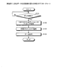
[実施例1に係るデータ伝送処理フロー]
次に、図16を用いて、実施例1に係るデータ伝送処理の流れを説明する。図16は、実施例1に係るデータ伝送処理の流れの例を示すフローチャートである。
[Data Transmission Processing Flow According to Embodiment 1]
Next, the flow of data transmission processing according to the first embodiment will be described with reference to FIG. FIG. 16 is a flowchart illustrating an example of the flow of data transmission processing according to the first embodiment.
まず、クライアントデータを受信した場合を説明する。例えば、図16に示すように、伝送装置100は、クライアントデータを受信した場合に(ステップS101肯定)、ネットワーク処理部130側で利用されている送信クロックでクロスコネクト用のフレームへのマッピング処理を実行する(ステップS102)。このとき、伝送装置100は、クライアントデータを受信していない場合に(ステップS101否定)、クライアントデータの受信待ちの状態となる。
First, a case where client data is received will be described. For example, as illustrated in FIG. 16, when the
そして、伝送装置100は、ネットワーク処理部130側で利用されている送信クロックでクロスコネクト処理を実行することでクロスコネクト処理を同期化する(ステップS103)。続いて、伝送装置100は、ネットワーク処理部130側において、利用している送信クロックで種々の処理を実行し、WDMネットワークにデータを伝送する(ステップS104)。
Then, the
次に、ネットワークデータを受信した場合を説明する。例えば、図16に示すように、伝送装置100は、ネットワークデータを受信した場合に(ステップS101肯定)、OTU2フレームから下位レイヤのODUk(k=0,1)フレームに分離する。さらに、伝送装置100は、ODUkフレームからクロスコネクト用のフレームへのマッピング処理を実行する(ステップS102)。このとき、伝送装置100は、ネットワークデータを受信していない場合に(ステップS101否定)、ネットワークデータの受信待ちの状態となる。
Next, a case where network data is received will be described. For example, as illustrated in FIG. 16, when the
そして、伝送装置100は、クロスコネクト処理を実行し(ステップS103)、クライアント処理部110側において、クライアント毎に種々の処理を実行し、クライアント装置にデータを送信する(ステップS104)。
Then, the
[実施例1による効果]
上述したように、伝送装置100は、非同期のクライアントデータを、ネットワーク側と同一のクロックに同期させてクロスコネクト処理を実行するので、装置全体の小型化を実現できる。要するに、伝送装置100は、非同期なクライアントデータのままクロスコネクト処理を実行するために、クライアントデータ毎にクロックを生成するPLL回路を要する従来技術と比較して、装置全体の小型化を実現できる。また、伝送装置100は、装置全体を小型化できるので、消費電力や発熱量を抑制することができる。
[Effects of Example 1]
As described above, the
さて、これまで本願に開示する伝送装置100の実施例について説明したが、上述した実施例以外にも種々の異なる形態にて実施されてよいものである。そこで、[構成]において異なる実施例を説明する。
Although the embodiments of the
[構成]
上記文書中や図面中等で示した処理手順、制御手順、具体的名称、各種のデータやパラメータ等を含む情報については、特記する場合を除いて任意に変更することができる。また、図示した伝送装置100の各構成要素は、機能概念的なものであり、必ずしも物理的に図示の如く構成されていることを要しない。すなわち、各装置の分散・統合の具体的形態は、図示のものに限られず、その全部又は一部を各種の負担や使用状況などに応じて、任意の単位で機能的または物理的に分散・統合することができる。例えば、クロック生成回路101は、ネットワーク処理部130が有することにしても良い。また、同様に、同期クロスコネクトスイッチ102は、ネットワーク処理部130が有することにしても良い。また、伝送装置100のハードウェア構成としては、一つの様態として、図2等に示したクライアント処理部110を複数合わせた1枚のFPGA(Field‐Programmable Gate Array)等の集積回路で実現する。また、さらには、クロック生成回路101、同期クロスコネクトスイッチ102、クライアント処理部110、ネットワーク処理部130等の機能を1枚のASIC(Application Specific Integrated Circuit)に搭載しても良い。また、さらには、クライアント処理部110、ネットワーク処理部130で行なう一部若しくは全ての処理のプログラムをメモリに格納し、メモリからプログラムをCPU(Central Processing Unit)等のプロセッサに読み出すことにより処理を実行するようにしても良い。
[Constitution]
Information including processing procedures, control procedures, specific names, various data, parameters, and the like shown in the above documents and drawings can be arbitrarily changed unless otherwise specified. The constituent elements of the illustrated
100 伝送装置
101 クロック生成回路
102 同期クロスコネクトスイッチ
103 PLL回路
110 クライアント処理部
111 光モジュール
112 セレクタ部
113 符号化部
114 フレーム生成回路
115 フレーム生成回路
116 フレーム終端回路
117 フレーム生成回路
118 フレーム終端回路
119 分離/多重回路
120 フレーム終端回路
121 フレーム終端回路
122 セレクタ部
123 クロスコネクトフレーム生成回路
130 ネットワーク処理部
131a〜131h クロスコネクト終端回路
132a〜132h フレーム終端回路
133 分離/多重回路
134 フレーム生成回路
135 光モジュール
DESCRIPTION OF
Claims (5)
データを受信する受信器と、
前記クロック生成回路によって生成されたクロックを利用して、前記受信器によって受信された非同期な複数のデータをクロスコネクト用のフレームへマッピングするマッピング回路と、
前記クロック生成回路によって生成されたクロックを利用して、前記マッピング回路によってマッピングされたクロスコネクト用のフレームをクロスコネクトするクロスコネクトスイッチと、
前記クロスコネクトスイッチによってクロスコネクトされたクロスコネクトフレームのデータを送信する送信器と
を有することを特徴とする伝送装置。 A clock generation circuit for generating a clock;
A receiver for receiving data;
A mapping circuit for mapping a plurality of asynchronous data received by the receiver to a frame for cross-connection using a clock generated by the clock generation circuit;
A cross-connect switch that cross-connects the cross-connect frame mapped by the mapping circuit using the clock generated by the clock generation circuit;
And a transmitter for transmitting data of a cross-connect frame cross-connected by the cross-connect switch.
クロックを生成し、
データを受信し、
前記生成したクロックを利用して、前記受信した非同期な複数のデータをクロスコネクト用のフレームへマッピングし、
前記生成したクロックを利用して、前記マッピングされたクロスコネクト用のフレームをクロスコネクトし、
前記クロスコネクトしたクロスコネクトフレームのデータを送信する
ことを特徴とするデータ伝送方法。 A data transmission method executed by a computer,
Generate a clock,
Receive data,
Using the generated clock, the received asynchronous data is mapped to a cross-connect frame,
Cross-connect the mapped cross-connect frame using the generated clock,
A data transmission method comprising transmitting data of the cross-connected cross-connect frame.
Priority Applications (2)
| Application Number | Priority Date | Filing Date | Title |
|---|---|---|---|
| JP2011118491A JP5736964B2 (en) | 2011-05-26 | 2011-05-26 | Transmission apparatus and data transmission method |
| US13/424,804 US9450693B2 (en) | 2011-05-26 | 2012-03-20 | Transmission apparatus and data transmission method |
Applications Claiming Priority (1)
| Application Number | Priority Date | Filing Date | Title |
|---|---|---|---|
| JP2011118491A JP5736964B2 (en) | 2011-05-26 | 2011-05-26 | Transmission apparatus and data transmission method |
Publications (2)
| Publication Number | Publication Date |
|---|---|
| JP2012249028A true JP2012249028A (en) | 2012-12-13 |
| JP5736964B2 JP5736964B2 (en) | 2015-06-17 |
Family
ID=47219185
Family Applications (1)
| Application Number | Title | Priority Date | Filing Date |
|---|---|---|---|
| JP2011118491A Expired - Fee Related JP5736964B2 (en) | 2011-05-26 | 2011-05-26 | Transmission apparatus and data transmission method |
Country Status (2)
| Country | Link |
|---|---|
| US (1) | US9450693B2 (en) |
| JP (1) | JP5736964B2 (en) |
Families Citing this family (3)
| Publication number | Priority date | Publication date | Assignee | Title |
|---|---|---|---|---|
| US9246617B2 (en) | 2013-09-09 | 2016-01-26 | Applied Micro Circuits Corporation | Reformating a plurality of signals to generate a combined signal comprising a higher data rate than a data rate associated with the plurality of signals |
| US9590756B2 (en) | 2013-09-16 | 2017-03-07 | Applied Micro Circuits Corporation | Mapping a plurality of signals to generate a combined signal comprising a higher data rate than a data rate associated with the plurality of signals |
| CN112042132A (en) * | 2018-04-13 | 2020-12-04 | 康普技术有限责任公司 | Configurable wide area distributed antenna system |
Citations (5)
| Publication number | Priority date | Publication date | Assignee | Title |
|---|---|---|---|---|
| JPH11266220A (en) * | 1998-03-18 | 1999-09-28 | Fujitsu Ltd | Transmitter of sdh system |
| WO2001047158A1 (en) * | 1999-12-20 | 2001-06-28 | Kabushiki Kaisha Toshiba | Transmitter and tributary interface board |
| JP2003188919A (en) * | 2001-12-19 | 2003-07-04 | Nec Corp | Network, switch device, method for processing otn frame to be used therefor, its circuit and integrated circuit |
| JP2008113344A (en) * | 2006-10-31 | 2008-05-15 | Nippon Telegr & Teleph Corp <Ntt> | Optical transmission system and method |
| JP2011223453A (en) * | 2010-04-13 | 2011-11-04 | Nippon Telegr & Teleph Corp <Ntt> | Digital cross-connect device and method |
Family Cites Families (8)
| Publication number | Priority date | Publication date | Assignee | Title |
|---|---|---|---|---|
| US7286487B2 (en) * | 2002-11-18 | 2007-10-23 | Infinera Corporation | Optical transmission network with asynchronous mapping and demapping and digital wrapper frame for the same |
| US8274892B2 (en) * | 2001-10-09 | 2012-09-25 | Infinera Corporation | Universal digital framer architecture for transport of client signals of any client payload and format type |
| CN1791278B (en) * | 2004-12-14 | 2010-04-14 | 华为技术有限公司 | Synchronous optical network and optical transmission network uniform dispatching system and its method |
| US7809017B2 (en) * | 2006-09-21 | 2010-10-05 | Nortel Networks Limited | Multi-rate transparent MUX for optical communications networks |
| CN101389146B (en) * | 2007-09-13 | 2011-01-05 | 华为技术有限公司 | Method and apparatus for synchronous crossed scheduling of optical transmission network |
| CN101610430B (en) * | 2009-06-30 | 2013-03-27 | 中兴通讯股份有限公司 | Method and device for realizing cross scheduling of ODUk |
| US8649400B2 (en) * | 2010-07-29 | 2014-02-11 | Ciena Corporation | Communication clock transport method and device |
| US8412040B2 (en) * | 2011-04-04 | 2013-04-02 | Infinera Corporation | Method and apparatus for mapping traffic using virtual concatenation |
-
2011
- 2011-05-26 JP JP2011118491A patent/JP5736964B2/en not_active Expired - Fee Related
-
2012
- 2012-03-20 US US13/424,804 patent/US9450693B2/en active Active
Patent Citations (5)
| Publication number | Priority date | Publication date | Assignee | Title |
|---|---|---|---|---|
| JPH11266220A (en) * | 1998-03-18 | 1999-09-28 | Fujitsu Ltd | Transmitter of sdh system |
| WO2001047158A1 (en) * | 1999-12-20 | 2001-06-28 | Kabushiki Kaisha Toshiba | Transmitter and tributary interface board |
| JP2003188919A (en) * | 2001-12-19 | 2003-07-04 | Nec Corp | Network, switch device, method for processing otn frame to be used therefor, its circuit and integrated circuit |
| JP2008113344A (en) * | 2006-10-31 | 2008-05-15 | Nippon Telegr & Teleph Corp <Ntt> | Optical transmission system and method |
| JP2011223453A (en) * | 2010-04-13 | 2011-11-04 | Nippon Telegr & Teleph Corp <Ntt> | Digital cross-connect device and method |
Also Published As
| Publication number | Publication date |
|---|---|
| US20120300771A1 (en) | 2012-11-29 |
| JP5736964B2 (en) | 2015-06-17 |
| US9450693B2 (en) | 2016-09-20 |
Similar Documents
| Publication | Publication Date | Title |
|---|---|---|
| US8699886B2 (en) | Externally synchronized optical transport network systems and associated methods | |
| US8934479B2 (en) | Super optical channel transport unit signal supported by multiple wavelengths | |
| US9225462B2 (en) | Method, apparatus and system for transmitting and receiving client signals | |
| US8494363B2 (en) | Signal format conversion apparatus and methods | |
| EP1881669B1 (en) | Implementing method and device for transmitting lan signals in otn | |
| US9608755B2 (en) | Network element clock synchronization systems and methods using optical transport network delay measurement | |
| JP4729049B2 (en) | Optical transmitter | |
| US20070264015A1 (en) | Uniform Switching System and Method for Synchronous Optical Network and Optical Transport Network | |
| JP5461229B2 (en) | Client signal accommodation multiplex processing device, client signal cross-connect device, and client signal accommodation multiplex processing method | |
| WO2008035769A1 (en) | Multiplex transmission system and multiplex transmission method | |
| CN103891222A (en) | Resizing existing traffic flow in optical transport network | |
| US9264283B2 (en) | Method of accommodating signals, frame generation apparatus, frame reception apparatus, and transmission system | |
| JP5078878B2 (en) | Method and apparatus for synchronous exchange of optical transport network signals | |
| US9621291B2 (en) | Optical communication cross-connection devices and signal processing method thereof | |
| JP5068376B2 (en) | Optical digital transmission system | |
| JP2008113344A (en) | Optical transmission system and method | |
| JP5699759B2 (en) | Transmission apparatus and transmission method | |
| JP5736964B2 (en) | Transmission apparatus and data transmission method | |
| EP2093916B1 (en) | Optical transport hierarchy gateway interface | |
| US9226050B2 (en) | Transmission apparatus and transmission method | |
| Ferrant et al. | OTN timing aspects | |
| JP4941547B2 (en) | Optical transmission apparatus and optical transmission method | |
| US20160142798A1 (en) | Transmission apparatus | |
| US20230198622A1 (en) | Providing Access To Client Overhead While Transparently Transmitting The Client Signal Over Multiple Optical Subcarriers | |
| EP2586143B1 (en) | Method and apparatus for forming and processing data units |
Legal Events
| Date | Code | Title | Description |
|---|---|---|---|
| A621 | Written request for application examination |
Free format text: JAPANESE INTERMEDIATE CODE: A621 Effective date: 20140204 |
|
| A977 | Report on retrieval |
Free format text: JAPANESE INTERMEDIATE CODE: A971007 Effective date: 20141106 |
|
| A131 | Notification of reasons for refusal |
Free format text: JAPANESE INTERMEDIATE CODE: A131 Effective date: 20150106 |
|
| A521 | Request for written amendment filed |
Free format text: JAPANESE INTERMEDIATE CODE: A523 Effective date: 20150309 |
|
| TRDD | Decision of grant or rejection written | ||
| A01 | Written decision to grant a patent or to grant a registration (utility model) |
Free format text: JAPANESE INTERMEDIATE CODE: A01 Effective date: 20150324 |
|
| A61 | First payment of annual fees (during grant procedure) |
Free format text: JAPANESE INTERMEDIATE CODE: A61 Effective date: 20150406 |
|
| R150 | Certificate of patent or registration of utility model |
Ref document number: 5736964 Country of ref document: JP Free format text: JAPANESE INTERMEDIATE CODE: R150 |
|
| LAPS | Cancellation because of no payment of annual fees |