US8699886B2 - Externally synchronized optical transport network systems and associated methods - Google Patents
Externally synchronized optical transport network systems and associated methods Download PDFInfo
- Publication number
- US8699886B2 US8699886B2 US11/592,663 US59266306A US8699886B2 US 8699886 B2 US8699886 B2 US 8699886B2 US 59266306 A US59266306 A US 59266306A US 8699886 B2 US8699886 B2 US 8699886B2
- Authority
- US
- United States
- Prior art keywords
- otn
- level
- synchronized
- odu
- network
- Prior art date
- Legal status (The legal status is an assumption and is not a legal conclusion. Google has not performed a legal analysis and makes no representation as to the accuracy of the status listed.)
- Active, expires
Links
- 230000003287 optical effect Effects 0.000 title claims abstract description 98
- 230000001360 synchronised effect Effects 0.000 title claims description 98
- 238000000034 method Methods 0.000 title claims description 54
- 230000005540 biological transmission Effects 0.000 claims abstract description 12
- 230000006978 adaptation Effects 0.000 claims description 51
- 230000008569 process Effects 0.000 claims description 45
- RGNPBRKPHBKNKX-UHFFFAOYSA-N hexaflumuron Chemical compound C1=C(Cl)C(OC(F)(F)C(F)F)=C(Cl)C=C1NC(=O)NC(=O)C1=C(F)C=CC=C1F RGNPBRKPHBKNKX-UHFFFAOYSA-N 0.000 abstract description 19
- 238000013459 approach Methods 0.000 abstract description 8
- 230000032258 transport Effects 0.000 description 48
- 238000013507 mapping Methods 0.000 description 18
- 239000013256 coordination polymer Substances 0.000 description 14
- 101100462419 Homo sapiens OTUB2 gene Proteins 0.000 description 12
- 101150046103 OTU2 gene Proteins 0.000 description 12
- 102100025914 Ubiquitin thioesterase OTUB2 Human genes 0.000 description 12
- 101100406673 Arabidopsis thaliana OTU3 gene Proteins 0.000 description 11
- 238000012360 testing method Methods 0.000 description 10
- 101100518559 Homo sapiens OTUB1 gene Proteins 0.000 description 9
- 101150115940 OTU1 gene Proteins 0.000 description 9
- 102100040461 Ubiquitin thioesterase OTUB1 Human genes 0.000 description 9
- 238000006243 chemical reaction Methods 0.000 description 8
- 230000009471 action Effects 0.000 description 5
- 239000013307 optical fiber Substances 0.000 description 5
- 238000001514 detection method Methods 0.000 description 4
- 238000001914 filtration Methods 0.000 description 4
- 230000035508 accumulation Effects 0.000 description 3
- 238000009825 accumulation Methods 0.000 description 3
- 238000003780 insertion Methods 0.000 description 3
- 230000037431 insertion Effects 0.000 description 3
- 239000011159 matrix material Substances 0.000 description 3
- 230000008901 benefit Effects 0.000 description 2
- 238000012937 correction Methods 0.000 description 2
- 238000013461 design Methods 0.000 description 2
- 238000009432 framing Methods 0.000 description 2
- 238000012423 maintenance Methods 0.000 description 2
- 239000000203 mixture Substances 0.000 description 2
- 230000008929 regeneration Effects 0.000 description 2
- 238000011069 regeneration method Methods 0.000 description 2
- 102220465832 La-related protein 1_F10A_mutation Human genes 0.000 description 1
- 229910052792 caesium Inorganic materials 0.000 description 1
- TVFDJXOCXUVLDH-UHFFFAOYSA-N caesium atom Chemical compound [Cs] TVFDJXOCXUVLDH-UHFFFAOYSA-N 0.000 description 1
- 239000000969 carrier Substances 0.000 description 1
- 150000001875 compounds Chemical class 0.000 description 1
- 238000005538 encapsulation Methods 0.000 description 1
- 238000012544 monitoring process Methods 0.000 description 1
- 230000006855 networking Effects 0.000 description 1
- 238000012545 processing Methods 0.000 description 1
- 238000012797 qualification Methods 0.000 description 1
- 238000012546 transfer Methods 0.000 description 1
- 230000007723 transport mechanism Effects 0.000 description 1
Images


Classifications
-
- H—ELECTRICITY
- H04—ELECTRIC COMMUNICATION TECHNIQUE
- H04J—MULTIPLEX COMMUNICATION
- H04J3/00—Time-division multiplex systems
- H04J3/16—Time-division multiplex systems in which the time allocation to individual channels within a transmission cycle is variable, e.g. to accommodate varying complexity of signals, to vary number of channels transmitted
- H04J3/1605—Fixed allocated frame structures
- H04J3/1652—Optical Transport Network [OTN]
- H04J3/1658—Optical Transport Network [OTN] carrying packets or ATM cells
-
- H—ELECTRICITY
- H04—ELECTRIC COMMUNICATION TECHNIQUE
- H04J—MULTIPLEX COMMUNICATION
- H04J3/00—Time-division multiplex systems
- H04J3/02—Details
- H04J3/06—Synchronising arrangements
- H04J3/07—Synchronising arrangements using pulse stuffing for systems with different or fluctuating information rates or bit rates
-
- H—ELECTRICITY
- H04—ELECTRIC COMMUNICATION TECHNIQUE
- H04J—MULTIPLEX COMMUNICATION
- H04J3/00—Time-division multiplex systems
- H04J3/02—Details
- H04J3/14—Monitoring arrangements
-
- H—ELECTRICITY
- H04—ELECTRIC COMMUNICATION TECHNIQUE
- H04J—MULTIPLEX COMMUNICATION
- H04J2203/00—Aspects of optical multiplex systems other than those covered by H04J14/05 and H04J14/07
- H04J2203/0001—Provisions for broadband connections in integrated services digital network using frames of the Optical Transport Network [OTN] or using synchronous transfer mode [STM], e.g. SONET, SDH
- H04J2203/0057—Operations, administration and maintenance [OAM]
- H04J2203/006—Fault tolerance and recovery
-
- H—ELECTRICITY
- H04—ELECTRIC COMMUNICATION TECHNIQUE
- H04J—MULTIPLEX COMMUNICATION
- H04J3/00—Time-division multiplex systems
- H04J3/02—Details
- H04J3/06—Synchronising arrangements
- H04J3/0635—Clock or time synchronisation in a network
- H04J3/0638—Clock or time synchronisation among nodes; Internode synchronisation
- H04J3/0644—External master-clock
-
- H—ELECTRICITY
- H04—ELECTRIC COMMUNICATION TECHNIQUE
- H04J—MULTIPLEX COMMUNICATION
- H04J3/00—Time-division multiplex systems
- H04J3/02—Details
- H04J3/06—Synchronising arrangements
- H04J3/0635—Clock or time synchronisation in a network
- H04J3/0685—Clock or time synchronisation in a node; Intranode synchronisation
- H04J3/0688—Change of the master or reference, e.g. take-over or failure of the master
-
- H—ELECTRICITY
- H04—ELECTRIC COMMUNICATION TECHNIQUE
- H04J—MULTIPLEX COMMUNICATION
- H04J3/00—Time-division multiplex systems
- H04J3/02—Details
- H04J3/06—Synchronising arrangements
- H04J3/0635—Clock or time synchronisation in a network
- H04J3/0685—Clock or time synchronisation in a node; Intranode synchronisation
- H04J3/0691—Synchronisation in a TDM node
Definitions
- the present invention relates generally to the telecommunications and optical networking fields. More specifically, the present invention relates to externally synchronized optical transport network (OTN) systems and associated methods.
- OTN optical transport network
- OTN multiplexing is an alternative to synchronous optical network/synchronous digital hierarchy (SONET/SDH) multiplexing, and its simplified justification scheme provides a number of advantages when multiplexing 2.5 Gbps signals and above.
- OTN multiplexing does not, however, address lower-rate signals (such as Gigabit Ethernet (GbE), T1, T3, etc.), which would require multiplexing into SONET/SDH or proprietary frame formats before being handled by an OTN multiplexer.
- GbE Gigabit Ethernet
- T1, T3, etc. Gigabit Ethernet
- the simplified OTN frame format, multiplexing scheme, and justification methodology provide for a more straightforward and scalable hardware design than SONET/SDH methodologies.
- G.709 Interfaces for the Optical Transport Network (OTN)” and G.798 “Characteristics of optical transport network hierarchy equipment functional blocks” (6/2004).
- OTN Optical Transport Network
- G.798 Charges of optical transport network hierarchy equipment functional blocks” (6/2004).
- OTN optical transport network
- OTH optical transport hierarchy
- G.798 covers the functional requirements of Optical Transport Network functionality within equipment.
- OTN multiplexing includes a layered structure including Optical Payload Unit of level k (OPUk) defined within Optical Data Unit of level k (ODUk), defined within Optical Transport Unit of level k (OTUk).
- OPUk is the information structure used to adapt client information for transport over an optical channel. It includes client information together with any overhead needed to perform rate adaptation between the client signal rate and the OPUk payload rate and other OPUk overhead supporting the client signal transport. This overhead is adaptation specific.
- the path optical data unit k (ODUkP) is the information structure used to support the end-to-end ODUk trail.
- the optical channel transport units of level k (OTUk and OTUkV) are the information structure used for transport of an ODUk over one or more optical channel connections.
- the OTUk is a completely standardized optical transmission unit of level k and the OTUkV is a functionally standardized optical transmission unit of level k.
- Each consists of the optical data unit and OTUk related overhead (forward error correction (FEC) and overhead for management of an optical channel connection). It is characterized by its frame structure, bit rate, and bandwidth.
- client streams such as OC48/STM-16 are mapped bit-for-bit, such that they can be transmitted bit-for-bit at the frequency at which they were initially received.
- No SONET/SDH framing is required for transmitting the transported signals.
- Each OC48/STM-16 is carried both 100% bit-transparently and with its original independent timing.
- OTN is transparent to the payload it transports within the ODUk and that the OTN layer does not need to transport network synchronization since network synchronization can be transported within the payload, i.e. by SONET/SDH client tributaries.
- OTN multiplexing For carriers wishing to provide wavelength services, OTN multiplexing provides a simpler, more straightforward, and ultimately more cost-effective, transport mechanism than SONET/SDH.
- OTN multiplexing is limited by the ITU-T specifically excluding network synchronization between network elements (NEs) from OTN specifications.
- jitter generation specification limits jitter to 100 mUI pkpk and 10 mUI rms.
- the present invention utilizes external synchronization to generate a completely standardized or functionally standardized optical transmission unit of level k (OTUk[V]) signal providing less jitter and wander build-up through a network of OTN network elements. This increases noise margins of transported signals and payloads.
- the present invention provides stratum-level synchronization utilizing a standards-based approach.
- rate adapters are included to provide m/n scaling of OTUk[V] signals to rates common in SONET and SDH synchronizers to provide line and loop distribution of timing through OTUk[V] signals.
- the present invention provides a choice of external synchronization sources including building integrated timing source (BITS), line, and loop timing sources.
- the present invention provides multiple external references and automated timing protection switching for redundancy and reliability.
- OTN transport was created to exclude the necessity of external synchronization. Jitter and wander noise are treated as component filtering problems, and addressed as such.
- the present invention incorporates external synchronization with OTN multiplexing as part of an overall system approach to solving jitter and wander noise problems.
- the present invention replaces a free run oscillator with a synchronization subsystem within various OTN adaptation source processes.
- the present invention includes a synchronization subsystem in place of the free run oscillator in the ODUkP to ODU[i]j adaptation source process.
- the present invention includes a synchronization subsystem in place of the free run oscillator in the ODUkP to CBRx adaptation source process.
- the synchronization subsystem is configured to accept an external timing reference signal and can include multiple input timing sources, line source pre-selection, line rate conversion, reference selection, pre-scaling, out-of-range (OOR) detection, stratum synchronization, and a clock multiplier for scaling reference rates.
- an externally synchronized optical transport network (OTN) network element includes circuitry configured to generate a completely standardized or functionally standardized optical transmission unit of level k (OTUk[V]); and a clock synchronizer subsystem connected to the circuitry, wherein the clock synchronizer subsystem is configured to generate an output clock synchronous with an active timing reference.
- the active timing reference can be selected from input sources to the clock synchronizer subsystem and the input sources to the clock synchronizer subsystem can include one or more of an external reference, a line reference, and a combination thereof.
- the clock synchronizer subsystem comprises an out-of-range detector configured to detect degraded or failed input sources and the clock synchronizer subsystem can perform n/m rate conversion to provide a compatible rate when utilizing the line references as the input source.
- the clock synchronizer subsystem includes holdover functionality when all input sources fail and free run functionality, wherein the free run functionality includes a free run oscillator which is provisioned as the active timing reference when provision and when all input sources fail and holdover cannot be used.
- the circuitry can be configured to perform the path optical data unit of level k (ODUkP) to constant bit rate signal of rate x (CBRx) adaptation source process while generating the OTUk[V] and the externally synchronized OTN network element includes either a network synchronized transponder or regenerator.
- ODUkP path optical data unit of level k
- CBRx constant bit rate signal of rate x
- the origin node can include an OTN multiplexer operable to generate a completely standardized or functionally standardized optical transmission unit of level k (OTUk[V]) signal with the network timing reference for synchronization.
- OTUk[V] optical transmission unit of level k
- one or more OTN signals are transmitted over an optical fiber utilizing dense wave division multiplexing (DWDM).
- DWDM dense wave division multiplexing
- the active timing reference can be selected from input sources, the input sources comprise one or more of an external reference, a line reference, and a combination thereof.
- FIGS. 1 a - 1 b illustrate synchronous and asynchronous network elements (NEs) in an exemplary network configuration.
- FIGS. 2 a - 2 b illustrate mapping noise through synchronous and asynchronous network elements (NEs).
- FIG. 3 illustrates the path optical data unit of level k (ODUkP) to optical data unit of level j and i (i is optional; i ⁇ j) (ODU[i]j) adaptation source function (ODUkP/ODU[i]j_A_So) in G.798 which creates the ODUk signal from a free running clock.
- FIG. 4 illustrates the processes associated with the ODUkP/ODU[i]j_A_So function.
- FIG. 5 illustrates an exemplary embodiment of the present invention for adding external synchronization to the OTN ODUkP to ODU[i]j adaptation source process, ODUkP/ODU[i]j_A_So.
- FIG. 6 illustrates an exemplary embodiment of a synchronized transmit clock reference generation circuit of the present invention.
- FIG. 7 illustrates an exemplary embodiment of network synchronized multiplexing utilizes a network synchronized ODUk Tx clock reference in place of a free-run clock in the ODUkP/ODU[i]j_A_So process to generate the ODUk frame.
- FIG. 8 illustrates an exemplary embodiment of network synchronized asynchronous multiplexing utilizes a network synchronized ODUk Tx clock reference in place of a free-run clock in the ODUkP/CBRx-a_A_So (ODUkP to constant bit rate signal of rate x (CBRx) adaptation source) process to generate the ODUk frame.
- ODUkP to constant bit rate signal of rate x (CBRx) adaptation source
- FIG. 9 illustrates possible locations for network synchronization insertion in the OTN ODUk and OTUk source functions according to an exemplary embodiment of the present invention.
- FIGS. 10 a - 10 c illustrate OTN regenerated transport systems for extending the reach of dense wave division multiplexed (DWDM) transport systems by performing optical to electrical to optical (O-E-O) regeneration along the transmission path.
- DWDM dense wave division multiplexed
- FIGS. 11 a - 11 c illustrate different OTN network element (NE) types such as terminal multiplexers, add/drop multiplexers, and multi-service NEs utilizing externally synchronized OTN multiplexing.
- NE OTN network element
- FIGS. 12 a - 12 c illustrate an OTN transponder and an OTN regenerator utilizing synchronized OTN multiplexing.
- the present invention utilizes external synchronization to generate a completely standardized or functionally standardized optical transmission unit of level k (OTUk[V]) signal providing less jitter and wander build-up through a network of OTN network elements. This increases noise margins of transported signals and payloads.
- the present invention provides stratum-level synchronization utilizing a standards-based approach.
- rate adapters are included to provide m/n scaling of OTUk[V] signals to rates common in SONET and SDH synchronizers to provide line and loop distribution of timing through OTUk[V] signals.
- the present invention provides a choice of external synchronization sources including building integrated timing source (BITS), line, and loop timing sources.
- the present invention provides multiple external references and automated timing protection switching for redundancy and reliability.
- the present invention replaces a free run oscillator with a synchronization subsystem within various OTN adaptation source processes.
- the present invention includes a synchronization subsystem in place of the free run oscillator in the ODUkP to ODU[i]j adaptation source process.
- the present invention includes a synchronization subsystem in place of the free run oscillator in the ODUkP to CBRx adaptation source process.
- the synchronization subsystem is configured to accept an external timing reference signal and can include multiple input timing sources, line source pre-selection, line rate conversion, reference selection, pre-scaling, out-of-range (OOR) detection, stratum synchronization, and a clock multiplier for scaling reference rates.
- FIGS. 1 a - 1 b illustrate synchronous and asynchronous network elements (NEs) in an exemplary network configuration.
- the timing signal from a single primary reference (PR) 11 is distributed to all NEs 10 in the network.
- the PR 11 can include a bits integrated timing source (BITS) clock or similar device.
- This timing distribution between NEs 10 can be accomplished through external, line, and loop timing interfaces.
- All NEs 10 have an internal stratum-level synchronizer circuit. The stratum level specifies accuracy, jitter and wander behavior, holdover behavior, and free-run accuracy. Multiple timing inputs can be provided to allow for flexibility in timing distribution, as well as backup sources for timing protection switching.
- Timing aggregates of all of the NEs 10 are derived from the common PR 11 .
- Payload 12 is adapted to the aggregate timing during the mapping/multiplexing process through byte-stuffing. Adapted payload is passed through subsequent NEs 10 with little timing adaptation, other than compensation for aggregate frame offsets.
- asynchronous NEs 15 some or all of the NEs 15 are timed to independent asynchronous oscillators in a mix of islands of NEs timed to internal local oscillators (LOs) 17 a - 17 e .
- the LOs 17 a - 17 e do not meet stratum-level requirements. There are a wide range of free-run accuracies and random drift rates between NEs 15 which result in continuously varying jitter and wander between NEs 15 .
- Each NE 15 aggregate is independently timed. Payload 12 is adapted to the aggregate timing during the mapping/multiplexing process through byte-stuffing at each NE 15 .
- Adapted payload is passed through subsequent NEs 15 and is re-adapted at each NE 15 based on LO offsets, relative LO drift, and aggregate frame offsets. Ultimately, the varying jitter and wander between NEs 15 limits the reach of the network and the type of payload which can be transported.
- FIGS. 2 a - 2 b illustrate mapping noise through synchronous and asynchronous NEs.
- input optical channel (OCn) byte streams 21 are adapted to the PR 11 in the first NE 10 a by byte-stuffing through a justification byte stuff 24 .
- OCn optical channel
- the input is adapted to the PR 11 , there is little additional justification in the adapted OCn bytes in aggregate of each subsequent NEs 22 .
- Wander control minimizes additional byte-stuffing and synchronized mapping noise is low as payload passes through synchronized NEs 23 . Noise from the initial NE timing adaptation is the main contributor.
- Noise from subsequent NEs is minimized due to very small offsets between NE clocks. Synchronized NEs minimize justification events associated with mapping thus reducing the level of mapping noise and minimize the filtering required when deriving the transmit clock for the de-mapped payload signal.
- payload is adapted to each NE's LO 17 a - 17 e by byte-stuffing. Additional justification is generated because each NE must adapt the payload locally as the payload passes through the asynchronous NEs 27 and previous NE byte-stuffs cause instantaneous payload rate changes requiring random byte-stuffs.
- Asynchronous mapping noise is high. Noise from the final NE 15 b adaptation is a major contributor and each previous adaptation adds random noise due to random and drifting offsets between NEs. Synchronized networks are required by SONET/SDH to minimize payload jitter and wander.
- Jitter and wander noise can build up as payload is transported in a network of asynchronous NEs.
- Each asynchronous NE in the network produces significant numbers of justification events to adapt the payload signal from the previous NE. These justifications are uncontrolled and result in large accumulations of jitter and wander noise.
- OTN does not provide for synchronization of network elements.
- ITU-T Recommendation G.8251 “The Control of Jitter and Wander within the Optical Transport Network (OTN)”, it states that the OTN physical layer is not required to transport network synchronization. More precisely, neither the ODUk nor any layers below it are required to transport synchronization. Further, it states that OTUk interfaces are not synchronization interfaces. G.8251 states that the transportation synchronization over SDH is adequate for OTN.
- Section 13 states that an OTN NE does not require synchronization interfaces, complex clocks with holdover mode nor SSM processing.
- OTN multiplexing is limited by the ITU-T specifically excluding network synchronization between network elements (NEs).
- Theoretical analysis and lab testing has been performed to validate the assertion that the OTN higher rate of justification opportunities and low 8 UI per opportunity could carry SONET/SDH signals without increasing jitter and wander noise above Generic Requirements (GR) and ITU-T limits. This may be true, but as testing has confirmed, jitter and wander noise accumulate to levels above that which network operators are comfortable with.
- the jitter generation specification limits jitter to 100 mUI pkpk and 10 mUI rms. Network operators prefer numbers below 90 mUI pkpk and 9 mUI rms.
- ODU[i]j stands for optical data unit of level j and i (i is optional; i ⁇ j).
- Tributary ports 32 include optical data unit of level j (ODUj) connection points (ODUj_CPs) 33 and optical data unit of level i (ODUi) connection points (ODUi_CPs) 34 .
- ODUkP/ODU[i]j_A_So 30 asynchronously maps the ODUj_CPs 33 and ODUi_CPs 34 client signal into ODTUjk[/ik] including justification control (JC) information.
- the ODTUjk[/ik] are multiplexed into the payload area of the OPUk.
- ODUkP/ODU[i]j_A_So 30 adds OPUk Overhead (RES, PT, MSI) and default ODUk Overhead through the ODUkP/ODU[i]j_A_So_MP (management point) 31 .
- OTN provides full transparency through encapsulation while maintaining carrier-grade performance through OTN management overhead and forward error correction.
- a single Optical Carrier level 48/Synchronous Transport Module-16 (OC48/STM-16) signal is mapped bit-for-bit into the payload area of an Optical Channel Payload Unit 1 (OPU 1 ), resulting in a 100% bit-transparent-OC48/STM-16 carried in the OPU 1 .
- Justification overhead is added, but when multiplexing into a higher-rate OTN signal, the locations are set to 0, indicating no justification.
- Overhead is added to indicate what type of payload is mapped into the OPU 1 .
- ODU 1 Optical Data Unit 1
- OAM&P operations, administration, maintenance, and provisioning
- the entire ODU 1 (including the OPU 1 and OC-48/STM-16) is mapped into an Optical Data Tributary Unit 12 (ODTU 12 ), providing a 100% bit-transparent carrier for the ODU 1 (including the OPU 1 and OC48/STM-16).
- Up to four ODU 1 s can be mapped into an Optical Channel Payload Unit 2 (OPU 2 ) ( ⁇ 10 Gbps), and up to sixteen ODU 1 s can be mapped into an Optical Channel Payload Unit 3 (OPU 3 ) ( ⁇ 40 Gbps).
- the four tributaries are mapped into the OPU 2 by byte-striping the individual ODTU 12 s into the OPU 2 payload area. Justification opportunities are shared among the four tributary ODTU 12 s over a repeating four OPU 2 frame cycle. In the first frame, one negative and up to two positive byte-stuff opportunities exist for the first tributary ODTU 12 .
- the negative justification opportunity in the OPU 2 overhead can be used to store a payload byte. If the ODTU 12 is slightly lower than the nominal rate, one or more payload bytes (positive justification opportunities) can be skipped over.
- the three justification overhead opportunities must be set to indicate whether a negative justification, no justification, or one or two positive justifications were performed.
- the second frame is used for justifying the second tributary, the third frame is used for the third tributary, and the fourth frame is used for the forth tributary, respectively.
- the next frame is again used for the first tributary and the process is continued on a modulo 4 basis.
- Multiplex signal overhead is added to the OPU 2 to indicate both tributary number and the type of tributary multiplexed.
- De-multiplexing is accomplished by pulling the ODU 1 s out of the OPU 2 , keeping in mind that the tributaries were byte-stripped into the OPU 2 and that the justification opportunities are shared between the tributaries on a modulo 4 basis.
- the individual OC48/STM-16 signals are removed bit-for-bit from the individual OPU 1 payloads.
- Justification is interpreted by a majority vote of the three justification overhead locations in the Optical Channel Payload Unit k (OPUk). If two justification locations indicate the same justification direction, then that direction is used.
- SONET/SDH justification requires a mixture of byte-stuffing (H3 and payload byte immediately following it) and pointer generation and interpretation to find the payload frame.
- H3 and payload byte immediately following it To operate in the presence of bit errors, a justification is indicated by inverting all of the odd, or all of the even, pointer bits. If eight of the ten bits, when compared to the previous frame pointer, indicate a justification, then that justification is used, unless there was a justification that occurred less than four frames previous.
- Removing the payload involves reading the pointer to locate the start of the payload frame. At that point, depending on the STS/AU mapping, 1-n columns of the payload are skipped and then the payload can be removed.
- the processes associated with the ODUkP/ODU[i]_A_So 40 function are specific processes for each ODUj_CP 33 a - b , ODUi_CP 34 a - b , and common processes for the compound (multiplexed) signal ODUkP_AP (access point) 35 are depicted.
- Each of the ODUj_CP 33 a - b and ODUi_CP 34 a - b include a data connection (CI_D), a clock connection (CI_Ck), a frame start connection (CI_FS), and a multi-frame start connection (CI_MFS) as inputs to the ODUkP/ODU[i]j_A_So 40 function.
- Each of the connections are input into frame/multi-frame alignment and justification functions 42 a - b , 43 a - b.
- the frame/multi-frame alignment and justification functions 42 a - b , 43 a - b extend the ODUj_CP 33 a - b , ODUi_CP 34 a - b with the frame alignment overhead (FAS and MFAS) as described in ITU-T G.709/Y.1331.
- the Mapping, frequency justification and bit rate adaptation functions provide an elastic store (buffer) process for the ODUj_CP 33 a - b , ODUi_CP 34 a - b client signals.
- the data signal ODUj[/i]_CI is written into the buffer under control of the associated input clock.
- the data is read out of the buffer and written onto the D, NJO, PJO 1 and PJO 2 bytes of the selected ODTUjk[/ik] frame under control of the ODUk clock and justification decisions as defined in 19.5/G.709/Y.1331.
- a justification decision is performed every fourth frame for the ODTU 12 , every sixteenth frame for the ODTU 13 and four times every sixteen frames for the ODTU 23 .
- Each justification decision results in a corresponding double positive, positive, negative or no justification action.
- the reading of 2 data bytes out of the buffer is cancelled once.
- No ODUj[/i] data shall be written onto the PJO 2 , PJO 1 and NJO byte.
- the reading of 1 data byte out of the buffer is cancelled once.
- No ODUj[/i] data shall be written onto the PJO 1 and NJO byte and data shall be written onto the PJO 2 byte.
- ODUj[/i] data shall be written onto the PJO 2 , PJO 1 and NJO byte. If no justification action is to be performed, ODUj[/i] data is written onto the PJO 2 and PJO 1 byte and no ODUj[/i] data shall be written onto the NJO byte.
- the ODUk frame that contains the PJO 2 , PJO 1 and NJO bytes depends on the time slot[s] of the ODTUjk[/ik].
- the multiplexer 41 function assigns the individual ODTUjk[/ik] to specific times slots of the OPUk payload area as defined by the multiplex structure (see 19.3 and 19.4.1 in ITU-T Rec. G.709/Y.1331).
- the multiplex structure identifier (MSI) 44 function inserts the TxMSI into the MSI byte positions of the PSI overhead as defined in 19.4/G.709/Y.1331.
- the TxMSI value and as such the multiplex structure is either fixed or configurable via MI_TxMSI.
- the payload type (PT) 45 function inserts code “0010 0000” (ODU multiplex structure) into the PT byte position of the PSI overhead as defined in 15.9.2.1/G.709/Y.1331.
- the reserved (RES) 46 function inserts all-0's into the RES bytes.
- all other bits of the ODUk overhead are sourced as “0”s, except the ODUk-PM STAT field which should be set to the value “normal path signal” (001).
- the adapted information data (AI_D) 48 connection outputs the results of the multiplexing of the ODTUjk[/ik] from all of the functions 41 , 44 , 45 , 46 , 47 .
- the ODUkP/ODU[i]j_A_So 40 function also includes adapted information for multi-frame start (AI_MFS) 49 , adapted information for frame start (AI_FS) 50 , and adapted information for a clock (AI_CK) 51 .
- the AI_MFS 49 and AI_FS 50 functions generate the (multi) frame start reference signals AI_FS 49 and AI_MFS 50 for the ODUk signal.
- the AI_FS 50 signal shall be active once per 122368 clock cycles.
- AI_MFS 49 shall be active once every 256 frames.
- the AI_CK 51 function generates a local ODUk clock (ODUkP_AI_CK) of “239/(239 ⁇ k)*4(k ⁇ 1)*2 488 320 kHz +/ ⁇ 20 ppm” from a free running clock generator 52 .
- the clock parameters including jitter and wander requirements, as defined in Annex A/G.8251 (ODCa clock) apply.
- the free running clock generator 52 does not support external synchronization, stratum levels, SSM, or holdover modes.
- FIG. 5 illustrates the ODUkP/ODU[i]j_A_So 40 function depicted in FIG. 4 with the free running clock generator 52 replaced with a clock synchronizer subsystem 54 .
- the clock synchronizer subsystem 54 includes a free run clock 52 a ; external, line, and loop timing interfaces 59 ; timing reference selection 58 ; timing rate adaptation 57 circuits; timing reference inputs 56 ; and a clock synchronizer 55 .
- the clock synchronizer subsystem 54 can support wander control, holdover, 1-n timing reference inputs with a frequency qualification circuit, free run input, and automatic reference switching.
- the present invention adds the clock synchronizer subsystem 54 in place of the free run clock generator 52 in the ODUkP/ODU[i]j_A_So 40 function with the existing functionality in ODUkP/ODU[i]j_A_So 40 remaining. Additionally, the clock synchronizer subsystem 54 can be added in place of a free run clock generator in other OTN adaptation functions to provide synchronization.
- the external, line, and loop timing interfaces 59 are input into the timing reference selection 58 circuit.
- the external, line, and loop timing interfaces 59 can include, for example, a local external timing source such as an atomic Cesium clock or a satellite-derived clock, line-derived timing by monitoring synch status bytes to ensure quality, or loop timing from other network elements.
- example reference sources include E1 or DS1 signals from a building integrated timing source (BITS) clock.
- the timing reference selection 58 circuit is configured to select one of the external, line, and loop timing interfaces 59 for input into the clock synchronizer 55 .
- the timing rate adaptation 57 circuit is provisionable to multiply by M and divide by N to adapt line and loop timing signals to an SDH or SONET timing reference.
- the clock synchronizer 55 outputs a clock signal to the AI_CK 51 , AI_FS 50 , AI_MFS 49 from FIG. 4 .
- externally-synchronized generation of an OTUkV signal provides less jitter and wander build-up through a network of OTN multiplexers providing increased noise margins of transported signals and payloads.
- Stratum level synchronization provides a standards-based synchronization approach that has been tested and verified in existing SONET/SDH transport networks.
- Rate adapters to provide m/n scaling of OTUk[V] signals to rates common in SONET/SDH-style synchronizers provides line and loop distribution of timing through OTUk[V] signals.
- Choice of external synchronization sources, including BITS, Line, and Loop timing sources provides flexibility in synchronization distribution network design. Multiple references and automated timing protection switching provide redundancy in timing references to allow reliable operation in the presence of timing network faults.
- Synchronization functions integrated with the multiplexer circuit pack allows multiplexers to offer synchronization functionality without burdening remaining circuit packs with unnecessary functionality. Synchronization on a per-NE basis allows many multiplexers to share a common synchronization function, reducing the costs per multiplexer when compared to integrating the synchronization functionality on each multiplexer.
- the inputs to the clock reference generation circuit 60 include a free run 61 clock, one or more external references 62 a - b , and one or more line references 63 a - b .
- the external references 62 a - b can include external inputs such as a BITS clock signal, an E1, etc.
- the line references 63 a - b can include line inputs such as an OC-N, STM-N, and OTUk[V].
- the clock reference generation circuit 60 is included in an externally synchronized OTN multiplexer as a replacement for a free run clock generator.
- the line references 63 a - b are pre-selected by a line pre-selection 64 circuit prior to line rate conversion.
- a line rate conversion 65 circuit performs n/m rate conversion when OTUk[V] signals are used for line references to provide inputs compatible with standard stratum synchronization circuits.
- a reference selection 66 a - b circuit selects one or more timing sources as reference(s) to a stratum synchronizer 69 . After the reference selection 66 a - b , a pre-scaling 67 a - b circuit provides further scaling to convert reference source rates if required to rates compatible with standard stratum synchronization circuits.
- an out-of-range (OOR) detection circuit 68 a - b is provided to detect degraded and failed timing references.
- the output of the OOR 68 a - b circuit is to the stratum synchronizer 69 .
- the stratum synchronizer 69 generates an output clock synchronous with the active timing reference source on the input. This output clock meets stratum requirements for wander and jitter.
- the stratum synchronizer 69 uses selected source status, OOR status, provisioning and internal fault detection to select active reference. This meets stratum requirements for clock switching. Further, the stratum synchronizer 69 provides holder functionality when all reference sources fail and provides free run 61 functionality when provisioned or when all reference sources fail and holdover cannot be used.
- the stratum synchronizer 69 outputs to a synchronized clock multiplier 70 which multiples the output to an appropriate rate for use as an OTUk[V] transmit clock.
- a transmit clock reference 71 is used to replace the free run clock in the various OTN adaptation functions such as the OTN ODUkP to ODU[i] adaptation source process, ODUkP/ODU[i]j_A_So.
- an exemplary embodiment of network synchronized multiplexing utilizes a network synchronized ODUk Tx clock reference 75 in place of a free-run clock in the ODUkP/ODU[i]j_A_So process 40 to generate the ODUk frame.
- the clock reference 75 can be divided/multiplied to achieve the correct ODUk rate.
- Each of the frame/multi-frame alignment (FAS/MFAS) and justification functions 42 a - b , 43 a - b include a FAS/MFAS insertion function 76 followed by an elastic store 77 connected to a justification control and JC generation function 78 .
- the elastic store 77 includes read/write functionality to accept incoming ODUj_CP and ODUi_CP signals at the ODUi/j CP rate.
- the elastic store 77 is emptied at the synchronous ODUk rate.
- the justification control and generation 78 inserts or removes stuff bytes to make up for differences between the rate of the input and output.
- an ODUk frame is generated with the network synchronized ODUk Tx clock reference 75 .
- the ODU[i]j tributaries at the connection points (CPs) 42 a - b , 43 a - b are adapted into a network synchronized frame by the ODUkP_ODU[i]j_A_So process 40 .
- the tributaries on the CPs 42 a - b , 43 a - b are de-multiplexed from the received ODUk and then multiplexed into a network synchronized ODUk frame.
- Bi-directional multiplexer-regenerator contains two synchronization circuits to perform synchronization in two directions at a common location.
- N-directional multiplexer-regenerator contains N synchronization circuits to perform synchronization in N directions at a common location.
- NxBi-directional multiplexer-regenerator contains 2 ⁇ N synchronization circuits to perform synchronization in 2 ⁇ N directions at a common location.
- an exemplary embodiment of network synchronized asynchronous multiplexing utilizes a network synchronized ODUk Tx clock reference 81 in place of a free-run clock in the ODUkP/CBRx-a_A_So (ODUkP to constant bit rate signal of rate x (CBRx) adaptation source) process 80 to generate the ODUk frame.
- the clock reference 81 can be divided/multiplied to achieve the correct ODUk rate.
- FIG. 8 illustrate the ODUkP/CBRx-a_A_So process 80 as an example, but any of the standard, or non-standard asynchronous mappings could be used with the present invention.
- An elastic store 82 includes read/write functionality to accept incoming CBRx_CP signals at the CBR_CP rate.
- the elastic store 82 is emptied at the synchronous ODUk rate referenced to the network synchronized ODUk Tx clock reference 81 .
- a justification control and JC bits generation circuit 83 connects to the elastic store and is configured to insert/remove stuff bytes to make up for the difference between the rate at the input and output.
- the ODUk frame is generated with the network synchronized clock reference 81 .
- the ODUk frame is generated with the network synchronized clock reference 81 with payload being de-mapped from the received ODUk and then mapped into a network synchronized ODUk frame.
- One way multiplexer-regenerator performs synchronization in one direction.
- Bi-directional multiplexer-regenerator contains two synchronization circuits to perform synchronization in two directions at a common location.
- N-directional multiplexer-regenerator contains N synchronization circuits to perform synchronization in N directions at a common location.
- NxBi-directional multiplexer-regenerator contains 2 ⁇ N synchronization circuits to perform synchronization in 2 ⁇ N directions at a common location.
- OTN ODUk and OTUk source functions 90 illustrate possible locations for network synchronization insertion according to an exemplary embodiment of the present invention.
- ODUkP/x_A_So adaptation functions 91 , 95 , 99 are modified to include external synchronization to generate synchronized ODUk frames.
- ODU 1 asynchronous adaptation function (ODU 1 P/x_A_So) 91 maps payloads of up to 2.5 Gbps into a path optical data unit of level 1 (ODU 1 P) access point (ODU 1 P_AP) which in turn is mapped into an ODU1 termination connection point (ODU 1 _TCP) by an ODU 1 termination source process (ODU 1 T) 92 .
- OTU 1 to ODU 1 adaptation function (OTU 1 [V]/ODU 1 _A_So) 93 maps the ODU 1 _TCP into an OTU 1 access point (OTU 1 _AP) which is mapped into an OTU 1 termination connection point (OTU1_TCP) by an OTU1V termination source process (OTU 1 [V]) 94 .
- ODU 2 asynchronous adaptation function (ODU 2 P/x_A_So) 95 maps payloads of up to 10 Gbps (i.e., up to four ODU 192 signals or one 10 Gbps payload) into a path optical data unit of level 2 (ODU 2 P) access point (ODU 2 P_AP) which in turn is mapped into an ODU 2 termination connection point (ODU 2 _TCP) by an ODU 2 termination source process (ODU 2 T) 96 .
- ODU 2 P/x_A_So asynchronous adaptation function
- OTU 2 to ODU 2 adaptation function (OTU 2 [V]/ODU 2 _A_So) 97 maps the ODU 2 _TCP into an OTU 2 access point (OTU 2 _AP) which is mapped into an OTU 2 termination connection point (OTU 2 _TCP) by an OTU 2 V termination source process (OTU 2 [V]) 98 .
- ODU 3 asynchronous adaptation function (ODU 3 P/x_A_So) 99 maps payloads of up to 40 Gbps (i.e., a combination of nxODU 1 _CP (connection points) and mxODU 2 _CP (connection points), or one 40 Gbps payload) into a path optical data unit of level 3 (ODU 3 P) access point (ODU 3 P_AP) which in turn is mapped into an ODU 3 termination connection point (ODU 3 _TCP) by an ODU 3 termination source process (ODU 3 T) 100 .
- OTU 3 to ODU 3 adaptation function (OTU 3 [V]/ODU 3 _A_So) 101 maps the ODU 3 _TCP into an OTU 3 access point (OTU 3 _AP) which is mapped into an OTU 3 termination connection point (OTU 3 _TCP) by an OTU 3 [V] termination source process (OTU 3 V) 102 .
- external network synchronization is added in any one of the ODUkP/x_A_So adaptation functions 91 , 95 , 99 to generate synchronized ODUk frames.
- the ODUkP/x_A_So adaptation functions 91 , 95 , 99 can be used to generate network synchronized ODUk signals if the input payload signal is network synchronized.
- non-standard ODUk adaptation functions, frame sizes, and frame rates can be used to map payloads and multiplex signals.
- network synchronization can be added at any ODUk adaptation function 91 , 95 , 99 , and in the case of multiplexers, at more than one ODUk adaptation function 91 , 95 , 99 .
- the network synchronization can be sourced from external signal inputs (e.g., BITS, DS1, E1); line signal inputs (e.g., OC-m, STM-n, OTUkV); through timing at transponders and regenerators; holdover during synchronization source faults; and free run during synchronization source faults, maintenance periods, or when no timing source is available.
- the present invention utilizes standard OTN sink functions with externally synchronized source functions.
- the OTN sink functions are unaffected by the external synchronization.
- the present invention utilizes standard ODUk termination functions and standard OTUk functions which are unaffected by the external synchronization.
- regenerated OTN transport systems 105 , 110 , 115 extend the reach of dense wave division multiplexed (DWDM) transport systems by performing optical to electrical to optical (O-E-O) regeneration along the transmission path.
- the regenerated OTN transport system 105 includes an origin node 106 where DWDM signals are transmitted, several regenerator nodes 107 where DWDM signals are regenerated, and a terminal node 108 where the DWDM signals are received. Additional regenerators 107 can be added along the path to extend the reach farther of the DWDM signals. However, as a signal passes through regenerators, a slight amount of jitter is added to the signal.
- the jitter degrades the signal slightly and if the signal is passed through too many regenerators, the signal can be degraded too much or become unusable. Jitter accumulation builds up especially quickly when many regenerator circuits are placed close to each other in highly integrated packages in an effort to reduce the cost of the overall regenerator. In a regenerator-based transport system as depicted in the regenerated OTN transport system 105 , the jitter accumulation limits the maximum reach of the system.
- the regenerator OTN transport system 110 includes an origin node 111 where DWDM signals are transmitted, several regenerator nodes 112 where DWDM signals are regenerated, re-synchronized nodes 1113 to remove accumulated jitter, and a terminal node 114 where the DWDM signals are received.
- the re-synchronized nodes 113 are placed after a span of regenerators 112 to remove accumulated jitter to allow the reach to be extended further through additional spans of regenerators 112 .
- re-synchronization adds mapping noise.
- mapping jitter can build up quickly to unacceptable levels limiting the overall reach of the regenerator OTN transport system 110 .
- the regenerator OTN transport system 115 includes an embodiment of the present invention to provide network synchronization in regards to OTN multiplexed DWDM systems.
- Regenerator OTN transport system 115 includes an origin node 116 where DWDM signals are transmitted, several regenerator nodes 117 where DWDM signals are regenerated, re-synchronized nodes 118 to remove accumulated jitter, and a terminal node 119 where the DWDM signals are received.
- the re-synchronized nodes 118 use common network timing according to an embodiment of the present invention to reduce mapping jitter build up to extend the reach even further than regenerator OTN transport system 110 .
- a terminal multiplexer 120 includes multiple tributary ports 122 which are multiplexed into an OTUk 123 signal.
- the terminal multiplexer 120 includes external timing 121 according to the present invention.
- the tributary ports 122 can include OC-48, STM-16, OC-192, and STM-64 signals which are multiplexed using OTN multiplexing to OTU 2 or OTU 3 signals.
- the OTN multiplexing in the terminal multiplexer 120 can occur within a multiplexer circuit pack, a tributary circuit pack, or another circuit pack such as a switch matrix.
- Example embodiments of the terminal multiplexer 120 include the CoreStream/RLS T-MUXCVR and the CN4200 MainX and F10A, all available from CIENA Corporation of Linthicum, Md.
- an add-drop multiplexer (ADM) 125 includes multiple tributary ports 127 and an east OTUk 128 a and a west OTUk 128 b output.
- the ADM 125 is configured to multiplex the tributary ports 127 to and from both OTUk 128 a - b directions.
- the ADM 125 includes external timing 126 according to the present invention.
- the tributary ports 127 can include OC-48, STM-16, OC-192, and STM-64 signals which are multiplexed using OTN multiplexing to OTU 2 or OTU 3 signals.
- the OTN multiplexing in the ADM 125 can occur within a multiplexer circuit pack, a tributary circuit pack, or another circuit pack such as a switch matrix.
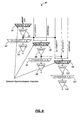
- a multi-service NE 130 includes multiple tributary ports 132 , multiple outputs OTUk 138 a - b , and multiple outputs OTUj 139 a - b .
- the multi-service NE 130 also can include a packet switch 133 , packet mapper 135 , cross-connect 136 matrix, SDH mapper 137 , and PDH mapper 134 .
- the multi-service NE 130 is configured to be a multi-service, multi-protocol switching system that consolidates the functionality of a multi-service switching platform (MSPP), digital cross-connect (DCS), Ethernet switch, and OTN switch in a single, high-capacity switching system.
- MSPP multi-service switching platform
- DCS digital cross-connect
- Ethernet switch and OTN switch in a single, high-capacity switching system.
- the multi-service NE 130 includes external timing 131 according to the present invention.
- the OTN multiplexing in the multi-service NE 130 can occur within a multiplexer circuit pack, a tributary circuit pack, the cross-connect 136 , the SDH mapper 137 , or another circuit pack.
- the tributary ports 132 can include signals such as OC-48, STM-16, OC-192, and STM-64 signals which are multiplexed using OTN multiplexing to OTU 2 or OTU 3 signals which are in turn sent to the cross-connect 136 and mapped to the OTUk,j 138 a - b , 139 a - b outputs.
- An example embodiment of the multi-service NE 130 is the CoreDirector available from CIENA Corporation of Linthicum, Md.
- client tributary ports 122 , 127 , 132 can be directly mapped into the ODUj[/i].
- Clients can include OTU 1 , OTU 2 , CBR 2 G 5 , Ethernet, and custom mappings. Additionally, clients can be mapped into other protocols before being mapped into the ODUj[/i] such as, for example, data ports mapped into generic framing protocol (GFP) then into the ODUj[/i], asynchronous transfer mode (ATM) extracted from a client then mapped into ODUj[/i], and multiplexing of virtually concatenated clients.
- GFP generic framing protocol
- ATM asynchronous transfer mode
- synchronized OTN multiplexing of the present invention can enhance the functionality of OTN transponders 140 , 145 and OTN regenerators 150 .
- the OTN transponder 140 includes an OC-m/STM-n 143 input, external or line timing 141 , and an OTUk[V] output 142 .
- the OC-m/STM-n 143 input payloads are asynchronously mapped into a synchronized OTUk[V] frame.
- the OTN transponder 145 includes an input 146 which can be any payload, external or line timing 141 , and an OTUk[V] output 142 .
- the input 146 can include any standard or non-standard payload signal/frame mapped into standard or non-standard rate OTUk[V] frames.
- the OTN regenerator 150 includes an OTUk[V] input 142 a , an OTUk[V] output 142 b , and external or line timing 141 .
- the OTN regenerator 150 de-maps payload received from the OTUk[V] input 142 a and re-maps it into a synchronized OTUk[V] output 142 b .
- an OTU 1 [V] can be de-mapped into an OC-48/STM-16 and then re-mapped into an OTU 1 [V]
- an OTU 2 [V] can be de-mapped into an OC-192/STM-64 and then re-mapped into an OTU 2 [V]
- an OTU 3 [V] can be de-mapped into an OC-768/STM-256 and then re-mapped into an OTU 3 [V].
- any standard or non-standard payload signal/frame can be de-mapped from a standard or non-standard rate OTUk[V] frame and mapped into standard or non-standard rate OTUk[V] frames.
- OTN multiplexing is defined in: ITU-T G.709 Interfaces for the optical transport network (OTN); ITU-T G.798 Characteristics of optical transport network hierarchy equipment functional blocks; OTN Standard FEC (Called GFEC sometimes) is defined in “ITU-T G.975”; OTN Jitter is defined in “ITU-T G.8251: The control of jitter and wander within the optical transport network (OTN)”; G.870: Terms and definitions for Optical Transport Networks (OTN); G.871: Framework for optical transport network Recommendations; G.873.1: Optical Transport Network (OTN): Linear protection; G.874: Management aspects of the optical transport network element; G.874.1: Optical transport network (OTN): Protocol-neutral management information model for the network element view; G.959.1: Optical transport network physical layer interfaces; G.8201: Error performance parameters and objectives for multi-operator international paths within the Optical Transport Network
Abstract
Description
Claims (17)
Priority Applications (1)
| Application Number | Priority Date | Filing Date | Title |
|---|---|---|---|
| US11/592,663 US8699886B2 (en) | 2005-11-23 | 2006-11-03 | Externally synchronized optical transport network systems and associated methods |
Applications Claiming Priority (2)
| Application Number | Priority Date | Filing Date | Title |
|---|---|---|---|
| US73911905P | 2005-11-23 | 2005-11-23 | |
| US11/592,663 US8699886B2 (en) | 2005-11-23 | 2006-11-03 | Externally synchronized optical transport network systems and associated methods |
Publications (2)
| Publication Number | Publication Date |
|---|---|
| US20070116061A1 US20070116061A1 (en) | 2007-05-24 |
| US8699886B2 true US8699886B2 (en) | 2014-04-15 |
Family
ID=38053463
Family Applications (1)
| Application Number | Title | Priority Date | Filing Date |
|---|---|---|---|
| US11/592,663 Active 2031-01-10 US8699886B2 (en) | 2005-11-23 | 2006-11-03 | Externally synchronized optical transport network systems and associated methods |
Country Status (1)
| Country | Link |
|---|---|
| US (1) | US8699886B2 (en) |
Cited By (2)
| Publication number | Priority date | Publication date | Assignee | Title |
|---|---|---|---|---|
| EP3301834A1 (en) * | 2016-09-30 | 2018-04-04 | Alcatel Lucent | Reference clock transmission via proprietary line frame signal |
| WO2019056912A1 (en) * | 2017-09-21 | 2019-03-28 | 烽火通信科技股份有限公司 | Clock processing device and method for otn tributary board |
Families Citing this family (27)
| Publication number | Priority date | Publication date | Assignee | Title |
|---|---|---|---|---|
| JP4729049B2 (en) * | 2005-12-22 | 2011-07-20 | 日本電信電話株式会社 | Optical transmitter |
| US7970008B2 (en) * | 2006-09-22 | 2011-06-28 | Nippon Telegraph And Telephone Corporation | Multiplexing transmission system and multiplexing transmission method |
| CN101232340B (en) * | 2007-01-23 | 2012-10-03 | 华为技术有限公司 | Communication system, method, transmission device as well as receiving apparatus |
| US7602814B2 (en) * | 2007-04-30 | 2009-10-13 | Ciena Corporation | Systems and methods for mapping and multiplexing wider clock tolerance signals in optical transport network transponders and multiplexers |
| JP4733766B2 (en) * | 2007-06-08 | 2011-07-27 | 富士通株式会社 | Jitter control device |
| CN101325465B (en) * | 2007-06-15 | 2010-10-27 | 华为技术有限公司 | Method for transmitting client signal in light transmission network and correlated equipment |
| CN101389146B (en) * | 2007-09-13 | 2011-01-05 | 华为技术有限公司 | Method and apparatus for synchronous crossed scheduling of optical transmission network |
| US7873073B2 (en) * | 2008-02-26 | 2011-01-18 | Ciena Corporation | Method and system for synchronous high speed Ethernet GFP mapping over an optical transport network |
| US20100014857A1 (en) * | 2008-07-17 | 2010-01-21 | Avalon Microelectronics, Inc. | Method of mapping OPUke into OTN frames |
| US8437641B2 (en) * | 2008-10-21 | 2013-05-07 | Bay Microsystems, Inc. | Clock regeneration for optical communications |
| CN102318238B (en) * | 2009-05-11 | 2014-12-31 | 华为技术有限公司 | Data transmission method, system and apparatus in an optical transport network |
| CN101616341B (en) * | 2009-08-05 | 2012-10-10 | 中兴通讯股份有限公司 | Method and device for cross protection |
| US8705402B2 (en) * | 2009-12-24 | 2014-04-22 | Infinera Corporation | Clocking of client signals output from an egress node in a network |
| CN101814968B (en) * | 2010-03-16 | 2014-06-11 | 中兴通讯股份有限公司 | Method and device for realizing frame header alignment and multi-frame zeroing |
| US8923347B2 (en) * | 2010-04-27 | 2014-12-30 | Transmode Systems Ab | Data transmission involving multiplexing and demultiplexing of embedded clock signals |
| CN101944952B (en) * | 2010-09-26 | 2015-05-20 | 中兴通讯股份有限公司 | Device and method for realizing overhead processing of optical transport network |
| CN102480415B (en) * | 2010-11-26 | 2015-10-21 | 中兴通讯股份有限公司 | A kind of method and device being recovered optical transport network clock by reference clock |
| US9143227B2 (en) | 2011-11-07 | 2015-09-22 | Ciena Corporation | Optical transport network port protection systems and methods using flexible switch criteria |
| US8817824B2 (en) | 2011-12-02 | 2014-08-26 | Ciena Corporation | Optical transport network line management system and methods |
| IN2012DE01073A (en) | 2012-04-09 | 2015-07-31 | Ciena Corp | |
| US9264139B2 (en) | 2012-05-21 | 2016-02-16 | Ciena Corporation | Optical transport network clock transient suppression systems and methods |
| US8898526B1 (en) * | 2012-07-23 | 2014-11-25 | Google Inc. | Using forward error correction coding to diagnose communication links |
| US9219938B2 (en) * | 2012-11-01 | 2015-12-22 | Wheatstone Corporation | System and method for routing digital audio data using highly stable clocks |
| US8958514B2 (en) * | 2013-07-12 | 2015-02-17 | IPLight Ltd. | Clock recovery in communication of hierarchically encapsulated signals |
| US10298348B2 (en) * | 2016-04-01 | 2019-05-21 | Ipg Photonics Corporation | Transparent clocking in a cross connect system |
| US10243722B2 (en) * | 2016-11-22 | 2019-03-26 | Huawei Technologies Co., Ltd. | Optical interconnecting network architecture |
| US11816051B1 (en) * | 2022-05-10 | 2023-11-14 | Juniper Networks, Inc. | Systems and methods for providing a global navigation satellite system capability to a time sensitive network device |
Citations (8)
| Publication number | Priority date | Publication date | Assignee | Title |
|---|---|---|---|---|
| US20030016416A1 (en) * | 2001-07-23 | 2003-01-23 | Alcatel | Network element for signals of the optical transport network (OTN) |
| US20030094982A1 (en) * | 2001-11-20 | 2003-05-22 | Zampetti George P. | Core sync module |
| US20030123493A1 (en) * | 2001-12-19 | 2003-07-03 | Nec Corporation | Network, switching apparatus and OTN frame processing method for use therein; its circuit and integrated circuit |
| US20030190003A1 (en) * | 2002-04-05 | 2003-10-09 | Fagerhoj Thomas O. | Selectable clocking architecture |
| US20040156325A1 (en) * | 2002-11-18 | 2004-08-12 | Perkins Drew D. | Optical transmission network with asynchronous mapping and demapping and digital wrapper frame for the same |
| US20050163162A1 (en) * | 2002-01-31 | 2005-07-28 | Marconi Communications Spa | Communications system |
| US7106968B2 (en) * | 2001-07-06 | 2006-09-12 | Optix Networks Inc. | Combined SONET/SDH and OTN architecture |
| US7542483B1 (en) * | 2003-06-25 | 2009-06-02 | Cisco Technology, Inc. | Recoverable reference clock architecture for SONET/SDH and ethernet mixed bidirectional applications |
-
2006
- 2006-11-03 US US11/592,663 patent/US8699886B2/en active Active
Patent Citations (9)
| Publication number | Priority date | Publication date | Assignee | Title |
|---|---|---|---|---|
| US7106968B2 (en) * | 2001-07-06 | 2006-09-12 | Optix Networks Inc. | Combined SONET/SDH and OTN architecture |
| US20030016416A1 (en) * | 2001-07-23 | 2003-01-23 | Alcatel | Network element for signals of the optical transport network (OTN) |
| US20030094982A1 (en) * | 2001-11-20 | 2003-05-22 | Zampetti George P. | Core sync module |
| US20030123493A1 (en) * | 2001-12-19 | 2003-07-03 | Nec Corporation | Network, switching apparatus and OTN frame processing method for use therein; its circuit and integrated circuit |
| US20050163162A1 (en) * | 2002-01-31 | 2005-07-28 | Marconi Communications Spa | Communications system |
| US20030190003A1 (en) * | 2002-04-05 | 2003-10-09 | Fagerhoj Thomas O. | Selectable clocking architecture |
| US20040156325A1 (en) * | 2002-11-18 | 2004-08-12 | Perkins Drew D. | Optical transmission network with asynchronous mapping and demapping and digital wrapper frame for the same |
| US7286487B2 (en) * | 2002-11-18 | 2007-10-23 | Infinera Corporation | Optical transmission network with asynchronous mapping and demapping and digital wrapper frame for the same |
| US7542483B1 (en) * | 2003-06-25 | 2009-06-02 | Cisco Technology, Inc. | Recoverable reference clock architecture for SONET/SDH and ethernet mixed bidirectional applications |
Cited By (2)
| Publication number | Priority date | Publication date | Assignee | Title |
|---|---|---|---|---|
| EP3301834A1 (en) * | 2016-09-30 | 2018-04-04 | Alcatel Lucent | Reference clock transmission via proprietary line frame signal |
| WO2019056912A1 (en) * | 2017-09-21 | 2019-03-28 | 烽火通信科技股份有限公司 | Clock processing device and method for otn tributary board |
Also Published As
| Publication number | Publication date |
|---|---|
| US20070116061A1 (en) | 2007-05-24 |
Similar Documents
| Publication | Publication Date | Title |
|---|---|---|
| US8699886B2 (en) | Externally synchronized optical transport network systems and associated methods | |
| US7602814B2 (en) | Systems and methods for mapping and multiplexing wider clock tolerance signals in optical transport network transponders and multiplexers | |
| US9608755B2 (en) | Network element clock synchronization systems and methods using optical transport network delay measurement | |
| US5841760A (en) | Transparent multiplexer/demultiplexer | |
| CA2387214C (en) | Hitless protection switching | |
| JP3811126B2 (en) | Method and apparatus for passing data in a network | |
| US6298038B1 (en) | Transparent transport | |
| US8934479B2 (en) | Super optical channel transport unit signal supported by multiple wavelengths | |
| US20080080860A1 (en) | Optical network system | |
| US20110243565A1 (en) | Network element for signals of the optical transport network (otn) | |
| US20090162061A1 (en) | Optical transmission system and method | |
| JP5078878B2 (en) | Method and apparatus for synchronous exchange of optical transport network signals | |
| US7002968B1 (en) | Transport system and transport method | |
| US8780897B2 (en) | Cross-connect system and cross-connect method | |
| EP3396880A1 (en) | Method for mapping digital signals into an optical transport network and corresponding network element, optical telecommunications network and frame for optical telecommunications network | |
| CA2472980C (en) | Communications system | |
| US8767802B2 (en) | Transmission device and transmission method | |
| ITMI20000545A1 (en) | METHOD AND APPARATUS TO TRANSMIT / RECEIVE STM-4 (SDH) OR STS-12 (SONET) LEVEL DIGITAL SIGNALS ON TWO RF CARRIERS IN A LINE SECTION | |
| JP5356865B2 (en) | Optical transmission apparatus and optical transmission method | |
| US20030152079A1 (en) | Method and apparatus for transporting a SDH/SONET client signal as a service | |
| US7526197B2 (en) | Utilizing the protecting bandwidth in a SONET network | |
| EP2093916B1 (en) | Optical transport hierarchy gateway interface | |
| JP3976693B2 (en) | Non-instantaneous switching system | |
| JP5736964B2 (en) | Transmission apparatus and data transmission method | |
| JP5354022B2 (en) | Transmission apparatus and signal transmission method |
Legal Events
| Date | Code | Title | Description |
|---|---|---|---|
| AS | Assignment |
Owner name: CIENA CORPORATION, MARYLAND Free format text: ASSIGNMENT OF ASSIGNORS INTEREST;ASSIGNORS:MEAGHER, KEVIN S.;ALLARD, JAMES M.;BROWN, MICHAEL S.;REEL/FRAME:018521/0958 Effective date: 20061103 |
|
| FEPP | Fee payment procedure |
Free format text: PAYOR NUMBER ASSIGNED (ORIGINAL EVENT CODE: ASPN); ENTITY STATUS OF PATENT OWNER: LARGE ENTITY |
|
| STCF | Information on status: patent grant |
Free format text: PATENTED CASE |
|
| AS | Assignment |
Owner name: DEUTSCHE BANK AG NEW YORK BRANCH, NEW YORK Free format text: SECURITY INTEREST;ASSIGNOR:CIENA CORPORATION;REEL/FRAME:033329/0417 Effective date: 20140715 |
|
| AS | Assignment |
Owner name: BANK OF AMERICA, N.A., AS ADMINISTRATIVE AGENT, NO Free format text: PATENT SECURITY AGREEMENT;ASSIGNOR:CIENA CORPORATION;REEL/FRAME:033347/0260 Effective date: 20140715 |
|
| MAFP | Maintenance fee payment |
Free format text: PAYMENT OF MAINTENANCE FEE, 4TH YEAR, LARGE ENTITY (ORIGINAL EVENT CODE: M1551) Year of fee payment: 4 |
|
| AS | Assignment |
Owner name: CIENA CORPORATION, MARYLAND Free format text: RELEASE BY SECURED PARTY;ASSIGNOR:DEUTSCHE BANK AG NEW YORK BRANCH;REEL/FRAME:050938/0389 Effective date: 20191028 |
|
| AS | Assignment |
Owner name: BANK OF AMERICA, N.A., AS COLLATERAL AGENT, ILLINO Free format text: PATENT SECURITY AGREEMENT;ASSIGNOR:CIENA CORPORATION;REEL/FRAME:050969/0001 Effective date: 20191028 |
|
| MAFP | Maintenance fee payment |
Free format text: PAYMENT OF MAINTENANCE FEE, 8TH YEAR, LARGE ENTITY (ORIGINAL EVENT CODE: M1552); ENTITY STATUS OF PATENT OWNER: LARGE ENTITY Year of fee payment: 8 |
|
| AS | Assignment |
Owner name: CIENA CORPORATION, MARYLAND Free format text: RELEASE BY SECURED PARTY;ASSIGNOR:BANK OF AMERICA, N.A.;REEL/FRAME:065630/0232 Effective date: 20231024 |