JP2012246156A - METHOD FOR PRODUCING GaAs SINGLE CRYSTAL AND GaAs SINGLE CRYSTAL WAFER - Google Patents
METHOD FOR PRODUCING GaAs SINGLE CRYSTAL AND GaAs SINGLE CRYSTAL WAFER Download PDFInfo
- Publication number
- JP2012246156A JP2012246156A JP2011117420A JP2011117420A JP2012246156A JP 2012246156 A JP2012246156 A JP 2012246156A JP 2011117420 A JP2011117420 A JP 2011117420A JP 2011117420 A JP2011117420 A JP 2011117420A JP 2012246156 A JP2012246156 A JP 2012246156A
- Authority
- JP
- Japan
- Prior art keywords
- gaas
- single crystal
- raw material
- gaas single
- concentration
- Prior art date
- Legal status (The legal status is an assumption and is not a legal conclusion. Google has not performed a legal analysis and makes no representation as to the accuracy of the status listed.)
- Granted
Links
- 239000013078 crystal Substances 0.000 title claims abstract description 153
- 229910001218 Gallium arsenide Inorganic materials 0.000 title claims abstract description 150
- 238000004519 manufacturing process Methods 0.000 title claims abstract description 37
- 239000002994 raw material Substances 0.000 claims abstract description 90
- VYPSYNLAJGMNEJ-UHFFFAOYSA-N Silicium dioxide Chemical compound O=[Si]=O VYPSYNLAJGMNEJ-UHFFFAOYSA-N 0.000 claims abstract description 85
- 235000012239 silicon dioxide Nutrition 0.000 claims abstract description 63
- 238000000034 method Methods 0.000 claims abstract description 56
- JKWMSGQKBLHBQQ-UHFFFAOYSA-N diboron trioxide Chemical compound O=BOB=O JKWMSGQKBLHBQQ-UHFFFAOYSA-N 0.000 claims abstract description 41
- 229910052810 boron oxide Inorganic materials 0.000 claims abstract description 40
- 239000007788 liquid Substances 0.000 claims abstract description 34
- 239000007787 solid Substances 0.000 claims abstract description 20
- 239000000377 silicon dioxide Substances 0.000 claims abstract description 18
- 229910004298 SiO 2 Inorganic materials 0.000 claims description 27
- 239000010453 quartz Substances 0.000 abstract description 45
- 239000012535 impurity Substances 0.000 abstract description 17
- 229910052796 boron Inorganic materials 0.000 abstract description 11
- 238000010438 heat treatment Methods 0.000 abstract description 10
- 230000008018 melting Effects 0.000 abstract description 10
- 238000002844 melting Methods 0.000 abstract description 10
- ZOXJGFHDIHLPTG-UHFFFAOYSA-N Boron Chemical compound [B] ZOXJGFHDIHLPTG-UHFFFAOYSA-N 0.000 abstract description 9
- JBRZTFJDHDCESZ-UHFFFAOYSA-N AsGa Chemical compound [As]#[Ga] JBRZTFJDHDCESZ-UHFFFAOYSA-N 0.000 description 135
- 235000012431 wafers Nutrition 0.000 description 44
- 230000000052 comparative effect Effects 0.000 description 25
- 238000003756 stirring Methods 0.000 description 20
- 238000007711 solidification Methods 0.000 description 16
- 230000008023 solidification Effects 0.000 description 16
- 239000000565 sealant Substances 0.000 description 15
- 239000003795 chemical substances by application Substances 0.000 description 11
- 238000007789 sealing Methods 0.000 description 11
- 238000006243 chemical reaction Methods 0.000 description 9
- 230000000694 effects Effects 0.000 description 9
- 239000000155 melt Substances 0.000 description 9
- KWYUFKZDYYNOTN-UHFFFAOYSA-M Potassium hydroxide Chemical compound [OH-].[K+] KWYUFKZDYYNOTN-UHFFFAOYSA-M 0.000 description 6
- 239000002019 doping agent Substances 0.000 description 6
- 238000003860 storage Methods 0.000 description 6
- LFQSCWFLJHTTHZ-UHFFFAOYSA-N Ethanol Chemical compound CCO LFQSCWFLJHTTHZ-UHFFFAOYSA-N 0.000 description 5
- 238000005259 measurement Methods 0.000 description 5
- 238000004090 dissolution Methods 0.000 description 4
- 238000009826 distribution Methods 0.000 description 4
- 229910052814 silicon oxide Inorganic materials 0.000 description 4
- 239000006104 solid solution Substances 0.000 description 4
- PZNSFCLAULLKQX-UHFFFAOYSA-N Boron nitride Chemical compound N#B PZNSFCLAULLKQX-UHFFFAOYSA-N 0.000 description 3
- DBKNIEBLJMAJHX-UHFFFAOYSA-N [As]#B Chemical compound [As]#B DBKNIEBLJMAJHX-UHFFFAOYSA-N 0.000 description 3
- 230000007423 decrease Effects 0.000 description 3
- 238000005530 etching Methods 0.000 description 3
- 238000011156 evaluation Methods 0.000 description 3
- 239000000463 material Substances 0.000 description 3
- XKRFYHLGVUSROY-UHFFFAOYSA-N Argon Chemical compound [Ar] XKRFYHLGVUSROY-UHFFFAOYSA-N 0.000 description 2
- IJGRMHOSHXDMSA-UHFFFAOYSA-N Atomic nitrogen Chemical compound N#N IJGRMHOSHXDMSA-UHFFFAOYSA-N 0.000 description 2
- 238000001816 cooling Methods 0.000 description 2
- 238000005520 cutting process Methods 0.000 description 2
- 230000007547 defect Effects 0.000 description 2
- 239000011810 insulating material Substances 0.000 description 2
- 229920006395 saturated elastomer Polymers 0.000 description 2
- 238000005204 segregation Methods 0.000 description 2
- 229910052710 silicon Inorganic materials 0.000 description 2
- 239000000758 substrate Substances 0.000 description 2
- OKTJSMMVPCPJKN-UHFFFAOYSA-N Carbon Chemical compound [C] OKTJSMMVPCPJKN-UHFFFAOYSA-N 0.000 description 1
- XUIMIQQOPSSXEZ-UHFFFAOYSA-N Silicon Chemical compound [Si] XUIMIQQOPSSXEZ-UHFFFAOYSA-N 0.000 description 1
- 229910052786 argon Inorganic materials 0.000 description 1
- 230000015572 biosynthetic process Effects 0.000 description 1
- 239000000969 carrier Substances 0.000 description 1
- 239000003153 chemical reaction reagent Substances 0.000 description 1
- 238000007796 conventional method Methods 0.000 description 1
- 238000002425 crystallisation Methods 0.000 description 1
- 230000008025 crystallization Effects 0.000 description 1
- 235000012489 doughnuts Nutrition 0.000 description 1
- 238000002194 freeze distillation Methods 0.000 description 1
- 239000007789 gas Substances 0.000 description 1
- 229910002804 graphite Inorganic materials 0.000 description 1
- 239000010439 graphite Substances 0.000 description 1
- 230000005484 gravity Effects 0.000 description 1
- 238000010348 incorporation Methods 0.000 description 1
- 239000011261 inert gas Substances 0.000 description 1
- 230000003993 interaction Effects 0.000 description 1
- 238000000691 measurement method Methods 0.000 description 1
- 229910052751 metal Inorganic materials 0.000 description 1
- 239000002184 metal Substances 0.000 description 1
- 229910052757 nitrogen Inorganic materials 0.000 description 1
- 230000003287 optical effect Effects 0.000 description 1
- 238000005498 polishing Methods 0.000 description 1
- 238000007517 polishing process Methods 0.000 description 1
- 230000002250 progressing effect Effects 0.000 description 1
- 230000001737 promoting effect Effects 0.000 description 1
- 238000006479 redox reaction Methods 0.000 description 1
- 239000010703 silicon Substances 0.000 description 1
- 229910001220 stainless steel Inorganic materials 0.000 description 1
- 239000010935 stainless steel Substances 0.000 description 1
- 238000006467 substitution reaction Methods 0.000 description 1
Images
Classifications
-
- C—CHEMISTRY; METALLURGY
- C30—CRYSTAL GROWTH
- C30B—SINGLE-CRYSTAL GROWTH; UNIDIRECTIONAL SOLIDIFICATION OF EUTECTIC MATERIAL OR UNIDIRECTIONAL DEMIXING OF EUTECTOID MATERIAL; REFINING BY ZONE-MELTING OF MATERIAL; PRODUCTION OF A HOMOGENEOUS POLYCRYSTALLINE MATERIAL WITH DEFINED STRUCTURE; SINGLE CRYSTALS OR HOMOGENEOUS POLYCRYSTALLINE MATERIAL WITH DEFINED STRUCTURE; AFTER-TREATMENT OF SINGLE CRYSTALS OR A HOMOGENEOUS POLYCRYSTALLINE MATERIAL WITH DEFINED STRUCTURE; APPARATUS THEREFOR
- C30B11/00—Single-crystal growth by normal freezing or freezing under temperature gradient, e.g. Bridgman-Stockbarger method
- C30B11/006—Controlling or regulating
-
- C—CHEMISTRY; METALLURGY
- C30—CRYSTAL GROWTH
- C30B—SINGLE-CRYSTAL GROWTH; UNIDIRECTIONAL SOLIDIFICATION OF EUTECTIC MATERIAL OR UNIDIRECTIONAL DEMIXING OF EUTECTOID MATERIAL; REFINING BY ZONE-MELTING OF MATERIAL; PRODUCTION OF A HOMOGENEOUS POLYCRYSTALLINE MATERIAL WITH DEFINED STRUCTURE; SINGLE CRYSTALS OR HOMOGENEOUS POLYCRYSTALLINE MATERIAL WITH DEFINED STRUCTURE; AFTER-TREATMENT OF SINGLE CRYSTALS OR A HOMOGENEOUS POLYCRYSTALLINE MATERIAL WITH DEFINED STRUCTURE; APPARATUS THEREFOR
- C30B11/00—Single-crystal growth by normal freezing or freezing under temperature gradient, e.g. Bridgman-Stockbarger method
-
- C—CHEMISTRY; METALLURGY
- C30—CRYSTAL GROWTH
- C30B—SINGLE-CRYSTAL GROWTH; UNIDIRECTIONAL SOLIDIFICATION OF EUTECTIC MATERIAL OR UNIDIRECTIONAL DEMIXING OF EUTECTOID MATERIAL; REFINING BY ZONE-MELTING OF MATERIAL; PRODUCTION OF A HOMOGENEOUS POLYCRYSTALLINE MATERIAL WITH DEFINED STRUCTURE; SINGLE CRYSTALS OR HOMOGENEOUS POLYCRYSTALLINE MATERIAL WITH DEFINED STRUCTURE; AFTER-TREATMENT OF SINGLE CRYSTALS OR A HOMOGENEOUS POLYCRYSTALLINE MATERIAL WITH DEFINED STRUCTURE; APPARATUS THEREFOR
- C30B27/00—Single-crystal growth under a protective fluid
-
- C—CHEMISTRY; METALLURGY
- C30—CRYSTAL GROWTH
- C30B—SINGLE-CRYSTAL GROWTH; UNIDIRECTIONAL SOLIDIFICATION OF EUTECTIC MATERIAL OR UNIDIRECTIONAL DEMIXING OF EUTECTOID MATERIAL; REFINING BY ZONE-MELTING OF MATERIAL; PRODUCTION OF A HOMOGENEOUS POLYCRYSTALLINE MATERIAL WITH DEFINED STRUCTURE; SINGLE CRYSTALS OR HOMOGENEOUS POLYCRYSTALLINE MATERIAL WITH DEFINED STRUCTURE; AFTER-TREATMENT OF SINGLE CRYSTALS OR A HOMOGENEOUS POLYCRYSTALLINE MATERIAL WITH DEFINED STRUCTURE; APPARATUS THEREFOR
- C30B29/00—Single crystals or homogeneous polycrystalline material with defined structure characterised by the material or by their shape
- C30B29/10—Inorganic compounds or compositions
- C30B29/40—AIIIBV compounds wherein A is B, Al, Ga, In or Tl and B is N, P, As, Sb or Bi
- C30B29/42—Gallium arsenide
Landscapes
- Chemical & Material Sciences (AREA)
- Engineering & Computer Science (AREA)
- Crystallography & Structural Chemistry (AREA)
- Materials Engineering (AREA)
- Metallurgy (AREA)
- Organic Chemistry (AREA)
- Inorganic Chemistry (AREA)
- Crystals, And After-Treatments Of Crystals (AREA)
Abstract
Description
本発明は、縦型ボート法によるGaAs単結晶の製造方法およびGaAs単結晶ウェハに関し、特に、高いキャリア濃度を有し、かつ、高い結晶性を有するGaAs単結晶の製造方法およびGaAs単結晶ウェハに関する。 The present invention relates to a method for producing a GaAs single crystal by a vertical boat method and a GaAs single crystal wafer, and more particularly to a method for producing a GaAs single crystal having a high carrier concentration and high crystallinity, and a GaAs single crystal wafer. .
GaAs(ガリウム砒素)デバイスの素材であるGaAs単結晶ウェハは、GaAs単結晶インゴットを厚さ数百μmのウェハ上に切断(スライシング)し、研磨工程などを経て製造される。シリコン(Si)を不純物として添加したSiドープn型GaAs単結晶ウェハは、DVDなどのレーザー用の基板や発光ダイオード(LED)などの発光素子用の基板として用いられている。 A GaAs single crystal wafer, which is a material of a GaAs (gallium arsenide) device, is manufactured by cutting (slicing) a GaAs single crystal ingot onto a wafer having a thickness of several hundreds μm and performing a polishing process or the like. A Si-doped n-type GaAs single crystal wafer doped with silicon (Si) as an impurity is used as a substrate for a laser such as a DVD or a substrate for a light emitting element such as a light emitting diode (LED).
ここで、GaAs単結晶インゴットの製造方法として、縦型温度傾斜法(VGF法)や縦型ブリッジマン法(VB法)といった縦型ボート法が知られている。縦型ボート法は、るつぼの底部に種結晶を配置し、その種結晶の上層に単結晶の原料融液と封止剤の液体を配置して、当該るつぼを所定の温度分布から冷却することにより、原料融液の下部から上方に向けて結晶を成長させる方法である。縦型温度傾斜法(VGF法)の場合、温度そのものを降温し、縦型ブリッジマン法(VB法)の場合、当該るつぼを所定の温度分布内で相対的に移動させる。SiドープGaAs単結晶インゴットを製造する場合には、GaAs融液中にSiを添加する。 Here, as a method for producing a GaAs single crystal ingot, a vertical boat method such as a vertical temperature gradient method (VGF method) or a vertical Bridgman method (VB method) is known. In the vertical boat method, a seed crystal is arranged at the bottom of a crucible, and a single crystal raw material melt and a sealant liquid are arranged above the seed crystal to cool the crucible from a predetermined temperature distribution. Thus, the crystal grows upward from the lower part of the raw material melt. In the case of the vertical temperature gradient method (VGF method), the temperature itself is lowered, and in the case of the vertical Bridgman method (VB method), the crucible is relatively moved within a predetermined temperature distribution. When manufacturing a Si-doped GaAs single crystal ingot, Si is added to the GaAs melt.
この方法では、揮発成分であるAsがインゴットから解離するのを防ぐ目的などのため、封止剤としてB2O3(酸化ホウ素)を用いる。結晶成長中、GaAs融液と液体B2O3との界面では、以下の反応式による酸化還元反応が起きることが知られている。
3Si(Melt中)+2B2O3=3SiO2(B2O3中へ)+4B(Melt中) ・・・(1)
上記反応式(1)は単結晶成長開始時にはほぼ平衡状態に達し、単結晶成長中はノーマルフリージングによる偏析現象によるSiのGaAs融液への濃縮がおこっているものと考えられる。
In this method, B 2 O 3 (boron oxide) is used as a sealant for the purpose of preventing the volatile component As from dissociating from the ingot. It is known that an oxidation-reduction reaction according to the following reaction formula occurs at the interface between the GaAs melt and liquid B 2 O 3 during crystal growth.
3Si (in Melt) + 2B 2 O 3 = 3SiO 2 (into B 2 O 3 ) + 4B (in Melt) (1)
The reaction formula (1) reaches an almost equilibrium state at the start of single crystal growth, and it is considered that Si is concentrated in the GaAs melt due to segregation phenomenon due to normal freezing.
ここで、上記反応式(1)が右辺側に進行すると、GaAs融液にはSiが減少する一方、液体封止剤からGaAs融液へホウ素(B)が混入することとなる。ホウ素の発生は、スカムと称される砒化ホウ素を主体とした異物の発生につながり、このスカムが原因となり、GaAsの単結晶化が妨げられたり、スリップ転位および伝播転位が発生したりして、GaAs単結晶の品質を下げる。 Here, when the reaction formula (1) proceeds to the right side, Si is reduced in the GaAs melt, while boron (B) is mixed into the GaAs melt from the liquid sealant. The generation of boron leads to the generation of foreign matter mainly composed of boron arsenide called scum, and this scum causes the single crystallization of GaAs, slip dislocation and propagation dislocation, Reduce the quality of GaAs single crystals.
特許文献1には、封止剤としてB2O3中に予めシリコン酸化物を添加したものを用いることで、上記反応式(1)の平衡を左辺側にした状態で結晶成長を進める技術が記載されている。また、特許文献2には、均一なキャリア濃度分布を有するSiドープGaAs単結晶を製造するため、結晶成長中に液体封止剤を撹拌する技術が記載されている。 Patent Document 1 discloses a technique for promoting crystal growth in a state where the balance of the above reaction formula (1) is set to the left side by using a sealing agent in which silicon oxide is added in advance in B 2 O 3. Are listed. Patent Document 2 describes a technique of stirring a liquid sealing agent during crystal growth in order to produce a Si-doped GaAs single crystal having a uniform carrier concentration distribution.
縦型ボート法は原料融液の下部から上方に向けて結晶を成長させるため、結晶に取り込まれなかった不純物は融液中に濃縮される。ここで、キャリア濃度を高めるべくGaAs融液中に添加するドーパントのSi(つまり、GaAs原料とともに投入するSi結晶)を多量にすると、上記反応式(1)の平衡が右辺側に進行し、GaAs融液中にホウ素(B)が多量に移動するため、結晶成長が進み不純物の濃縮が進むにつれて砒化ホウ素の発生も進行し、高い結晶性を得ることができなくなる。つまり、GaAs単結晶ではキャリア濃度と結晶性とが二律背反の関係にある。現在多く使用されるn型導電性のGaAsウェハは、1×10¹⁸〜2×1018cm−3のキャリア濃度を有するものが主流であるが、近年、2×1018cm−3より高いキャリア濃度を有する高キャリア濃度のGaAsウェハに対するニーズも高まっている。 In the vertical boat method, the crystal is grown upward from the lower part of the raw material melt, so that impurities not taken into the crystal are concentrated in the melt. Here, when the dopant Si added to the GaAs melt to increase the carrier concentration (that is, Si crystal added together with the GaAs raw material) is increased, the equilibrium of the reaction formula (1) proceeds to the right side, and GaAs Since a large amount of boron (B) moves into the melt, generation of boron arsenide progresses as crystal growth progresses and impurity concentration progresses, and high crystallinity cannot be obtained. That is, in a GaAs single crystal, the carrier concentration and crystallinity are in a trade-off relationship. Currently, n-type conductive GaAs wafers frequently used have a carrier concentration of 1 × 10 18 to 2 × 10 18 cm −3 , but in recent years, carriers higher than 2 × 10 18 cm −3 are used. There is also a growing need for high carrier concentration GaAs wafers with high concentrations.
本発明者らは、2×1018cm−3より高いキャリア濃度を得るのに必要な量のSiを融液中に添加し、特許文献1および特許文献2の方法でSiドープGaAs単結晶を製造した。しかしながら、結晶成長の後半において2×1018cm−3より高いキャリア濃度の領域が得られたとしても、Siの添加に伴い、インゴット中のB濃度が高くなりすぎ、上記のとおり結晶性が悪化してしまう、具体的には当該インゴットから得た2×1018cm−3より高いキャリア濃度のウェハのエッチピット密度(EPD)が高いという問題があった。つまり、特許文献1および特許文献2の技術では、現在要求されているレベルでSi濃度とボロン濃度との関係(キャリア濃度と結晶性との関係)を両立できないことがわかった。 The inventors added an amount of Si necessary for obtaining a carrier concentration higher than 2 × 10 18 cm −3 into the melt, and formed a Si-doped GaAs single crystal by the methods of Patent Document 1 and Patent Document 2. Manufactured. However, even if a region having a carrier concentration higher than 2 × 10 18 cm −3 is obtained in the latter half of the crystal growth, the B concentration in the ingot becomes too high with the addition of Si, and the crystallinity deteriorates as described above. Specifically, there is a problem that the etch pit density (EPD) of a wafer having a carrier concentration higher than 2 × 10 18 cm −3 obtained from the ingot is high. That is, it has been found that the techniques of Patent Document 1 and Patent Document 2 cannot achieve the relationship between Si concentration and boron concentration (relationship between carrier concentration and crystallinity) at the level currently required.
そこで本発明は、上記課題に鑑み、高いキャリア濃度を有し、かつ、高い結晶性を有するGaAs単結晶の製造方法およびGaAs単結晶ウェハを提供することを目的とする。 In view of the above problems, an object of the present invention is to provide a method for producing a GaAs single crystal having a high carrier concentration and high crystallinity, and a GaAs single crystal wafer.
この目的を達成すべく本発明者らがさらに検討を行ったところ、GaAs単結晶の低転位化を目指す過程で、不純物としてのホウ素(B)の不純物硬化効果に着目した。不純物硬化とは固溶硬化ともよばれ、不純物原子が置換型あるいは格子間型として材料中に固溶すると、強度が増加する現象のことである。不純物効果は、固溶原子と転位との相互作用により転位を下げる効果がある。一般的にGaAsでは、Siによる不純物硬化効果が大きいことが知られている。しかし、本発明者らがさらに検討したところ、GaAsに適量のホウ素が含まれている場合も、Si程顕著ではないものの、不純物硬化効果が認められることが判明した。そして、GaAs融液における砒化ホウ素の発生を抑制しつつ、ホウ素(B)の不純物硬化効果をも得て十分に低いEPDを実現するためには、GaAs単結晶中のB濃度を1.9×10¹⁸〜6×1018cm−3の範囲内となるように不純物量を制御すればよいことを見出した。そのために、上記反応式(1)の平衡に抗うように、高いSi濃度においてもB濃度を上記範囲内に収められるように結晶成長系の工夫を検討した。そして、本発明者らは、原料収容時にGaAs原料と封止剤となる酸化ホウ素原料との間に固体の二酸化ケイ素(SiO2)を配置させることにより、上記の目的を達成できることを見出し、本発明を完成させるに至った。 As a result of further studies by the present inventors to achieve this object, attention was focused on the impurity hardening effect of boron (B) as an impurity in the process of reducing the dislocation of the GaAs single crystal. Impurity hardening is also called solid solution hardening, and is a phenomenon in which the strength increases when impurity atoms are dissolved in a material as a substitution type or an interstitial type. The impurity effect has an effect of lowering the dislocation by the interaction between the solid solution atom and the dislocation. In general, GaAs is known to have a large impurity hardening effect due to Si. However, as a result of further studies by the present inventors, it was found that even when a suitable amount of boron is contained in GaAs, an impurity hardening effect is recognized, although not as remarkable as Si. In order to achieve the sufficiently low EPD by suppressing the generation of boron arsenide in the GaAs melt and also obtaining the boron (B) impurity hardening effect, the B concentration in the GaAs single crystal is set to 1.9 ×. It has been found that the amount of impurities may be controlled so as to be in the range of 10 18 to 6 × 10 18 cm −3 . For this purpose, in order to resist the equilibrium of the reaction formula (1), a device for the crystal growth system was examined so that the B concentration can be kept within the above range even at a high Si concentration. The inventors have found that the above object can be achieved by disposing solid silicon dioxide (SiO 2 ) between a GaAs raw material and a boron oxide raw material that becomes a sealant when the raw material is accommodated. The invention has been completed.
すなわち、上記課題に鑑み、本発明の要旨構成は以下の通りである。
(1)種結晶、不純物となるSi原料およびGaAs原料、固体の二酸化ケイ素、ならびに酸化ホウ素原料をるつぼ内に収容した状態で縦型ボート法を行い、GaAs単結晶を成長させることを特徴とするGaAs単結晶の製造方法。
That is, in view of the above problems, the gist of the present invention is as follows.
(1) It is characterized in that a GaAs single crystal is grown by performing a vertical boat method in a state where seed crystals, Si raw materials and GaAs raw materials to be impurities, solid silicon dioxide, and boron oxide raw materials are housed in a crucible. A method for producing a GaAs single crystal.
(2)前記酸化ホウ素原料中には予めSiO2が添加されており、
前記酸化ホウ素原料中のSiO2のSi量および前記固体の二酸化ケイ素中のSi量の合計が、前記酸化ホウ素原料の質量に対して5質量%を超える上記(1)に記載のGaAs単結晶の製造方法。
(2) SiO 2 is added in advance to the boron oxide raw material,
The total amount of Si in SiO 2 in the boron oxide raw material and the amount of Si in the solid silicon dioxide exceeds 5% by mass with respect to the mass of the boron oxide raw material. Production method.
(3)前記GaAs単結晶の成長過程における所定期間に、前記酸化ホウ素原料が溶融した液体酸化ホウ素の撹拌を行う上記(1)または(2)に記載のGaAs単結晶の製造方法。 (3) The method for producing a GaAs single crystal according to (1) or (2), wherein the liquid boron oxide in which the boron oxide raw material is melted is stirred during a predetermined period in the growth process of the GaAs single crystal.
(4)キャリア濃度が2×1018cm−3より高く、エッチピット密度の最大値が500cm−2以下であることを特徴とするSiドープGaAs単結晶ウェハ。 (4) A Si-doped GaAs single crystal wafer having a carrier concentration higher than 2 × 10 18 cm −3 and a maximum etch pit density of 500 cm −2 or less.
本発明によれば、原料収容時にGaAs原料と封止剤となる酸化ホウ素原料との間に固体の二酸化ケイ素を配置させておき、縦型ボート法によりGaAs単結晶を成長させることにより、高いキャリア濃度においてもホウ素(B)濃度を低く抑えることができ、その結果、インゴット全体に亘って高いキャリア濃度を有し、かつ、高い結晶性を有するGaAs単結晶を製造することが可能となった。そして、このGaAs単結晶から、高いキャリア濃度を有しかつ高い結晶性を有するGaAs単結晶ウェハを得ることが可能となった。 According to the present invention, a high carrier is obtained by placing solid silicon dioxide between a GaAs raw material and a boron oxide raw material serving as a sealing agent when the raw material is accommodated, and growing a GaAs single crystal by a vertical boat method. Also in terms of concentration, the boron (B) concentration can be kept low, and as a result, a GaAs single crystal having a high carrier concentration and high crystallinity over the entire ingot can be produced. From this GaAs single crystal, a GaAs single crystal wafer having a high carrier concentration and high crystallinity can be obtained.
以下、図面を参照しつつ本発明の実施形態を説明する。 Hereinafter, embodiments of the present invention will be described with reference to the drawings.
(単結晶製造装置)
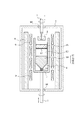
まず、本発明の実施形態によるGaAs単結晶の製造方法に用いる単結晶製造装置を、図1を用いて説明する。本実施形態の製造方法は、縦型ボート法(縦型温度傾斜法および縦型ブリッジマン法)によるものである。図1は、縦型ボート法を実施する単結晶製造装置の概略構成を示す断面図である。るつぼ4内に各種原料が収納されて結晶育成が行われる。るつぼ4は略円筒形状で、上側は開口され、下側は次第に径が小さくなるように断面テーパ状に形成されて閉じられたもので、最下端の小径部に種結晶10が収納される。
(Single crystal manufacturing equipment)
First, a single crystal manufacturing apparatus used for a GaAs single crystal manufacturing method according to an embodiment of the present invention will be described with reference to FIG. The manufacturing method of this embodiment is based on the vertical boat method (vertical temperature gradient method and vertical Bridgman method). FIG. 1 is a cross-sectional view illustrating a schematic configuration of a single crystal manufacturing apparatus that performs a vertical boat method. Various raw materials are stored in the
るつぼ4は、底を有する円筒状のるつぼ収納容器3内に収納される。るつぼ収納容器3は下部ロッド1に支持されている。この下部ロッド1は、図示しない駆動機構によって上下および回転の動作ができるようになっており、るつぼ収納容器3と該るつぼ収納容器3に収納されたるつぼ4を上下および回転駆動できるようになっている。
The
るつぼ収納容器3は、円筒状のヒーター9内に設置されている。このヒーター9は、それぞれ独立に温度の設定ができる複数のヒーターによって構成されており、るつぼ収納容器3に所望の温度勾配・温度分布を形成できるようになっている。ヒーター9の外側には、円筒状の断熱材8が配置され、これらは気密容器5に収納されている。
The crucible storage container 3 is installed in a
気密容器5の下部には下部ロッド1を貫通させる貫通孔が形成され、この貫通孔にシールリング6Aが嵌め込まれており、下部ロッド1が気密容器5の気密を維持しつつ上下および回転運動ができるようになっている。また、気密容器5の上部には上部ロッド2を貫通させる貫通孔が形成され、この貫通孔にシールリング6Bが嵌め込まれており、上部ロッド2が気密容器5の気密を維持しつつ上下および回転運動ができるようになっている。
A through-hole that allows the lower rod 1 to pass through is formed in the lower part of the
上部ロッド2は、図示しない駆動機構によって上下および回転の動作ができるようになっており、その先端部には、撹拌板7が取り付けられている。撹拌板7は、略四角形状の1枚の板体が上部ロッド2の先端部の取り付け部に略垂直に取り付けられているものである。撹拌板7の板体は、るつぼ4の内径の1/2以上の横幅と後述する液体封止剤層の厚さの1/2以上の縦幅を有することが好ましい。また、この板体を2枚以上設けてもよい。さらには、撹拌板7は液体封止剤の酸化ホウ素(B2O3)の融液を撹拌できるものであれば原則としてどの様な形状のものであってよい。
The upper rod 2 can be moved up and down and rotated by a driving mechanism (not shown), and a stirring plate 7 is attached to the tip of the upper rod 2. The stirring plate 7 is a substantially rectangular plate body attached to a mounting portion at the tip of the upper rod 2 substantially vertically. It is preferable that the plate body of the stirring plate 7 has a horizontal width of 1/2 or more of the inner diameter of the
図1はGaAs単結晶の成長中のるつぼ状態を示しており、融液部15であるGaAs融液の下部が、固化部20として成長したSiドープGaAs単結晶である。なお、るつぼ4や撹拌板7は、必要な耐熱性を有し、原料融液と反応しにくい材料であればよく、例えば、石英、熱分解窒化ホウ素(PBN:Pyrolytic Boron Nitride)を被覆したグラファイトなどが使用できる。本装置は、固液界面を上昇させるうえでの適切な温度勾配を得るために、るつぼ4の上下位置を固定してヒーター9の温度勾配を調整する方法(縦型温度傾斜法)にも、ヒーター9の温度勾配を固定してるつぼ4の上下位置を変える方法(縦型ブリッジマン法)にも適用することができる。
FIG. 1 shows a crucible state during the growth of a GaAs single crystal. The lower part of the GaAs melt as the
(GaAs単結晶の製造方法)
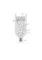
次に、本発明の実施形態によるGaAs単結晶の製造方法を、図1〜図3を用いて説明する。この製造方法では、図3に示すように、種結晶10、不純物となるSi原料12およびGaAs原料14、例えば円板形状の石英板などの固体の二酸化ケイ素16、ならびに酸化ホウ素原料18をるつぼ4内にこの順に収容した状態で縦型ボート法を行い、GaAs単結晶20を成長させることを特徴とし、かかる構成を採用することによって、高いキャリア濃度においてもB濃度を低く抑えることができ、その結果、高いキャリア濃度を有し、かつ、高い結晶性を有するGaAs単結晶を製造することが可能となった。
(Method for producing GaAs single crystal)
Next, a method for producing a GaAs single crystal according to an embodiment of the present invention will be described with reference to FIGS. In this manufacturing method, as shown in FIG. 3, a
以下、具体的に説明する。本実施形態では、上述の単結晶製造装置によって、以下のようにしてSiドープGaAs単結晶を製造する。まず、図3に示すように、るつぼ4内に、種結晶10、不純物(ドーパント)となるSi原料12およびGaAs原料14、石英板16、ならびに液体封止剤原料としてのB2O3原料18をこの順に収容する。
This will be specifically described below. In the present embodiment, a Si-doped GaAs single crystal is manufactured as follows using the above-described single crystal manufacturing apparatus. First, as shown in FIG. 3, in the
次に、これら原料を収容したるつぼ4を装置内にセットし、以下のようにして縦型ボート法を行う。まず、気密容器5内を真空引きし、アルゴン(Ar)、窒素などの不活性ガスで置換して、容器内を3〜9気圧に加圧した状態にする。そして、ヒーター9でるつぼ4を加熱し、種結晶10を除く各原料を溶融させていく。このとき、るつぼ4内は1200℃〜1450℃程度まで加熱される。ここで、ドーパントSi原料12の融点は1420℃、GaAs原料14の融点は1240℃、酸化ホウ素原料18は550℃付近を軟化点とし、一方、二酸化ケイ素の融点(軟化点)は1700℃である。そのため、加熱開始後、まず酸化ホウ素原料18が軟化し、液体酸化ホウ素19となる。次にGaAs原料14が融解し、GaAs融液15となる。この過程でSi原料12の一部はGaAs融液15に溶解し、またSi原料12の他の一部は液体酸化ホウ素19中にSiO2として取り込まれる。一方、同時に、石英板16は液体酸化ホウ素19中へ徐々に溶解していく。石英板16の溶解が進む間は、比重の関係から、GaAs融液15と液体B2O319との界面に石英板16が位置する。石英板が完全に溶解するか、飽和して一部溶け残るかについては後述する。なお、予めSiが溶解している液体酸化ホウ素19中へ、さらに石英板16が溶けるのは、るつぼ4内の高温により酸化ホウ素中のSiの固溶限界が上がり、その固溶限界までSiを溶解させることができる状態を、本発明により作ることができたからと考えられる。
Next, the
次に、GaAs種結晶105の上限側を溶融し、GaAs融液15となじませ、その後、GaAs融液15をるつぼ4の下部の種結晶10に接する部分から冷却・固化させる。具体的には、縦型温度傾斜法の場合は、ヒーター9を徐々に降温させていく。縦型ブリッジマン法の場合は、下部ロッド1によりるつぼ4をヒーター9に対して下に相対移動させる。固化が次第に上方に進行していく過程で、種結晶10からGaAs単結晶20が上方に成長していく。GaAs融液15の全量が固化したら、ヒーター9を降温し、るつぼ4の冷却を行う。るつぼ4が室温付近となった段階で、単結晶製造装置1の炉を開放して、液体封止剤を除去し、GaAs単結晶を取り出す。
Next, the upper limit side of the GaAs seed crystal 105 is melted and blended with the
このように、GaAs原料14と酸化ホウ素原料18との間に固体の二酸化ケイ素16を配置した状態で縦型ボート法の加熱を開始することにより得たSiドープGaAs単結晶インゴットは、高いキャリア濃度においてもB濃度を低く抑えることができ、キャリア濃度が2×1018cm−3より高くても、GaAs単結晶中のB濃度を1.9×10¹⁸〜6×1018cm−3の範囲内とすることができるようになった。この理由は必ずしも明らかではないが、本発明者らは以下のように推定している。すなわち、本実施形態では、結晶成長終了後に封止剤をアルコール溶解したときに見つかる固体の石英の割合が初期の石英板16の量に対し非常に少ない。結晶成長中の封止剤(液体酸化ホウ素19)とGaAs融液15の界面の状態を観察することができないため、一連のGaAs単結晶の結晶成長工程に含まれる加熱〜固化〜冷却のどの過程での石英板16がどのような状態かを把握することは困難であるが、原料溶融時点では既にGaAs融液15と液体B2O319との界面近傍に、極めてSiO2濃度の高い層(SiO2高濃度層17)が形成されていると考えられる。これにより、原料融解時から結晶成長時にわたって、反応式(1)の平衡を著しく左辺にシフトすることが可能になり、得られたGaAs単結晶20中のキャリア濃度およびB濃度を従来では不可能だった範囲に制御することができるものと思われる。
Thus, the Si-doped GaAs single crystal ingot obtained by starting the heating in the vertical boat method with the
石英板16の寸法(すなわちSiO2添加量)、形状は特に限定されず、製造装置、目的とするインゴットの寸法、目的とする単結晶中のSi濃度およびB濃度に合わせて設定することができるが、以下のように設定することが好ましい。固体の二酸化ケイ素16の形状は球状、多角形の板状、ドーナツ状などでも良いが、溶融後の液体B2O319下層に高濃度のSiO2層17を形成するため、円形の板状であることが好ましい。また、固体の二酸化ケイ素16としてのSiO2添加量は、液体B2O319に対して、3〜6質量ppmの範囲内とすることが好ましい。3質量ppm未満の場合、B2O3中に予めシリコン酸化物を添加する従来の方法との効果の差が十分に得られないおそれがあり、6質量ppmを超える場合、本発明の効果が飽和することが想定されるからである。また、固体の二酸化ケイ素16を石英板とした場合、結晶成長開始時におけるGaAs融液15の上面の面積に占める石英板16の面積の割合は、5〜99%が好ましく、90〜99%がより好ましい。同重量の石英板16をチャージする場合、石英板の形状をより広く薄くした方が溶融後のB2O3下層に高濃度SiO2層17を形成しやすいためである。
The dimensions (namely, the amount of SiO 2 added) and the shape of the
また、酸化ホウ素原料18中にはSi成分として予めSiO2が添加されており、酸化ホウ素原料18中のSiO2のSi量および固体の二酸化ケイ素16中のSi量の合計が、酸化ホウ素原料18の質量に対して5質量%を超えることが好ましい。また、上記割合は5質量%超え7質量%以下の範囲がより好ましく、5質量%超え〜5.5質量%以下の範囲がさらに好ましい。特許文献1のように液体封止剤であるB2O3中にシリコン酸化物を予め添加する場合、液体B2O3の質量に対して最大でも5質量%、通常の費用では3質量%以下しか溶解させることができない。これは、シリコン酸化物を溶解したB2O3を製造する過程で、高温時の濃度均一化および冷却時の均一なガラス化が困難であるためである。しかし、縦型ボート法の原料チャージ時に石英板16を用い原料融解時にB2O3下層に高濃度のSiO2層17を形成することによって、GaAs融液15の上面近傍に存在するSiO2量を飛躍的に、すなわちSi量で5質量%を超える値に高めることができる。その結果、反応式(1)の平衡を大きく左側にシフトさせることができる。
Further, SiO 2 is added in advance as a Si component in the boron oxide raw material 18, and the total of the Si amount of SiO 2 in the boron oxide raw material 18 and the Si amount in the
なお、全くSiが溶解していない液体酸化ホウ素19を用いた場合、単独で5質量%を超える量の石英板16を配置したとしても、縦型ボート法の加熱を開始後、GaAs融液15の上面近傍に存在する酸化ホウ素中のSi量のみが飽和して石英板16が大きく溶け残る可能性がある。そのため、酸化ホウ素19全体へSiが拡散する状態になりにくく、本発明の効果の再現性が十分に得られない可能性がある。そのため、予め均一にSiが添加された酸化ホウ素原料18を用いて、酸化ホウ素原料の質量に対して5質量%を超えるSi量となるように石英板16を配置することが好ましい。
In addition, when the
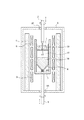
また、GaAs単結晶の成長過程における所定期間に、液体封止剤19であるB2O3の撹拌を行うことが好ましい。撹拌を行うことにより、所望する高いキャリア濃度範囲で、かつB濃度を低く抑えるという効果をより十分に発揮することができる。通常、GaAs中のSiはGaAs固化過程で偏析するため、固化の最終段階でできた結晶中のSi濃度は、固化の初期段階でできた結晶中のSi濃度の4〜5倍になる。SiはGaAs中でキャリアとして働くため、キャリア濃度も4〜5倍になる。ここで、B2O3部分を撹拌し、その結果としてB2O3下層の高濃度のSiO2層も撹拌されることで、GaAs融液15と接するB2O3下層のSi濃度が下がり、GaAs融液中のSiをB2O3中に取り込み、より狭いキャリア濃度範囲の結晶を効率良く得ることが可能となる。さらに、GaAs中のSiは、1×10¹⁹/cm3程度の高濃度になると、ドナーとしてだけではなくアクセプターとしても振る舞い、互いに相殺してしまう。この観点からも高キャリア濃度の場合はSiが偏析する結晶成長後半で攪拌を行う事が望ましい。
Moreover, it is preferable to stir B 2 O 3 which is the
具体的には、結晶成長中の所定の固化率の時点で、図2に示すように、上部ロッド2を下方に移動し、撹拌板7を液体封止剤19に浸漬させ、上部ロッド2を回転駆動して撹拌板7を回転させ、液体封止剤19を撹拌する。撹拌の回転数は2〜4rpmとする。また、撹拌を開始する固化率は0.05〜0.4とする。撹拌を終了する固化率は0.8〜1.0とする。ここで、本明細書において「固化率」とは、GaAs原料全体の重量に対して固化している部分の重量の比率を意味する。固化率は、固化が進行して結晶が成長していくにしたがって0から1まで増大していく。したがって、固化率がある特定の値であるということは、固化している部分と融液の部分とが接する界面が、固化率の値に1対1に対応した特定の位置にあることを意味する。これによって特定される位置は、全部が固化されて結晶が完成された後にも当然同じである。したがって、完成された単結晶の結晶成長方向における位置を固化率で特定することができる。
Specifically, at a predetermined solidification rate during crystal growth, as shown in FIG. 2, the upper rod 2 is moved downward, the stirring plate 7 is immersed in the
(SiドープGaAs単結晶ウェハ)
次に、本発明の実施形態によるSiドープGaAs単結晶ウェハを説明する。このウェハは、上記の製造方法によって製造されたインゴットを切断、研磨などして得ることができる。このインゴットは、キャリア濃度が2×1018cm−3より高くても、GaAs単結晶中のB濃度を1.9×10¹⁸〜6×1018cm−3の範囲内とすることができる。このため、本実施形態のウェハは、キャリア濃度が2×1018cm−3より高くても、エッチピット密度EPDの最大値が500cm−2以下という高い結晶性を有することを特徴とする。さらにキャリア濃度が2.2×1018cm−3より高く、または3×1018cm−3より高くても、エッチピット密度EPDの最大値が500cm−2以下という高い結晶性を有することができる。さらに、エッチピット密度EPDの平均値は25cm−2以下である。なお、本実施形態でキャリア濃度は概ね2.2〜3.5×1018cm−3の範囲となる。また、EPDの下限は特に限定されず、ウェハによってはゼロとなる場合もあるが、概ね0〜20cm−2の範囲となる。
(Si-doped GaAs single crystal wafer)
Next, a Si-doped GaAs single crystal wafer according to an embodiment of the present invention will be described. This wafer can be obtained by cutting, polishing, etc. the ingot produced by the above production method. Even if this ingot has a carrier concentration higher than 2 × 10 18 cm −3 , the B concentration in the GaAs single crystal can be in the range of 1.9 × 10 18 to 6 × 10 18 cm −3 . For this reason, the wafer of the present embodiment is characterized in that even if the carrier concentration is higher than 2 × 10 18 cm −3 , the maximum value of the etch pit density EPD is as high as 500 cm −2 or less. Furthermore, even if the carrier concentration is higher than 2.2 × 10 18 cm −3 or higher than 3 × 10 18 cm −3 , the maximum value of the etch pit density EPD can be high crystallinity of 500 cm −2 or less. . Furthermore, the average value of the etch pit density EPD is 25 cm −2 or less. In the present embodiment, the carrier concentration is generally in the range of 2.2 to 3.5 × 10 18 cm −3 . The lower limit of EPD is not particularly limited, and may be zero depending on the wafer, but is generally in the range of 0 to 20 cm −2 .
ここで本発明において、各ウェハのキャリア濃度は、Van der Pauw法を用いたホール測定により求めるものとする。 Here, in the present invention, the carrier concentration of each wafer is obtained by hole measurement using the Van der Pauw method.
また、EDPとその測定方法について簡単に説明する。例えば、GaAs単結晶のウェハが結晶欠陥を含んでいる場合、このウェハを特定の腐食性試薬中に浸漬すると結晶欠陥部よりエッチングが始まり、そこにピット(へこみ)が形成される。そこでエッチピット密度すなわち、単位面積あたりのエッチングにより形成されたピット数を計測すれば、当該ウェハの結晶性を評価することができる。そして、Siドープインゴットの所定箇所から作製したウェハのEPD評価を行えば、当該Siドープインゴットの結晶性を評価することができる。 Moreover, EDP and its measuring method are demonstrated easily. For example, when a GaAs single crystal wafer contains crystal defects, when this wafer is immersed in a specific corrosive reagent, etching starts from the crystal defect portion, and pits (dents) are formed there. Therefore, the crystallinity of the wafer can be evaluated by measuring the etch pit density, that is, the number of pits formed by etching per unit area. And if EPD evaluation of the wafer produced from the predetermined location of Si dope ingot is performed, the crystallinity of the said Si dope ingot can be evaluated.
本発明におけるEPDの測定方法は、あるウェハを液温320℃の溶融KOH(水酸化カリウム)に30分浸漬させてエッチングすることで生じたピットを光学顕微鏡により観察し、1mm2以上の測定視野でピットの数を計測することにより得る(規格SEMI M36−0699に準拠した方法)。なお、測定点数はウェハ面積によって異なるが、3インチウェハの場合37点である。 In the EPD measurement method of the present invention, a pit produced by immersing a wafer in molten KOH (potassium hydroxide) at a liquid temperature of 320 ° C. for 30 minutes and etching it is observed with an optical microscope, and a measurement field of 1 mm 2 or more. By measuring the number of pits (method according to standard SEMI M36-0699). The number of measurement points varies depending on the wafer area, but it is 37 points for a 3-inch wafer.
また、EPDの最大値とは、複数の測定点のうちの最大のEPD値を意味する。現在GaAs単結晶ウェハが使用されるデバイスメーカーにおいては、EPDは平均値だけでなく、その最大値も仕様化されている。最大値が低いことは、すなわちそのウェハのどの部分でも品質が高いということであり、歩留まりの面からも重要であるため、ウェハの結晶性の評価の好適な指標となる。 The EPD maximum value means the maximum EPD value among a plurality of measurement points. In device manufacturers that currently use GaAs single crystal wafers, EPD is specified not only for the average value but also for its maximum value. A low maximum value means that any part of the wafer is high in quality, and is important from the viewpoint of yield, and is therefore a suitable index for evaluating the crystallinity of the wafer.
上述したところは本発明の代表的な実施形態の例を示したものであって、本発明はこれらの実施形態に限定されるものではない。また、以下、実施例を用いて本発明をさらに詳細に説明するが、本発明は以下の実施例に何ら限定されるものではない。 The above description shows examples of typical embodiments of the present invention, and the present invention is not limited to these embodiments. In addition, the present invention will be described below in more detail with reference to examples, but the present invention is not limited to the following examples.
(実施例1)
図1に示した構成を有する、ステンレスチャンバーを用いた3インチ用GaAs単結晶の製造装置を用いて、以下の手順でGaAs単結晶インゴットを作製した。円筒形のPBN製のるつぼに、以下の順で原料を充填し、チャンバー内の所定の位置に配置した。
1.GaAs種結晶
2.GaAs原料であるGaAs多結晶6.0kgおよびSi結晶1200mg(GaAsに対して200質量ppm)
3.石英板(円板形状を2枚重ねたもの)9.1g
4.予めSiO2を添加し、Siを4.0質量%含有するB2O3原料360g
るつぼの上部から観察すると、ルツボの内径80mm対し石英板の直径は75mmである。また、B2O3原料中のSi量および石英板中のSi量の合計は、18.7gであり、B2O3原料の質量360gの5.2質量%に相当する。
Example 1
Using a 3-inch GaAs single crystal manufacturing apparatus using a stainless steel chamber having the configuration shown in FIG. 1, a GaAs single crystal ingot was manufactured according to the following procedure. The cylindrical PBN crucible was filled with the raw materials in the following order and placed at a predetermined position in the chamber.
1. 1. GaAs seed crystal GaAs polycrystal 6.0kg and Si crystal 1200mg (200ppm by mass with respect to GaAs)
3. Quartz plate (two stacked discs) 9.1g
4). 360 g of B 2 O 3 raw material containing 4.0% by mass of Si previously added with SiO 2
When observed from the upper part of the crucible, the diameter of the quartz plate is 75 mm with respect to the inner diameter of the crucible of 80 mm. The total amount of Si in the B 2 O 3 raw material and the Si amount in the quartz plate is 18.7 g, which corresponds to 5.2 mass% of the mass of the B 2 O 3 raw material of 360 g.
その後、装置内を真空引きし、Arガスで置換し、6気圧まで加圧した。ヒーターによりるつぼを加熱しながら8気圧まで加圧し、GaAs原料、Si原料、および種結晶の上部を溶融させた。以降は結晶成長終了まで8気圧を維持した。GaAs原料、Si原料、および種結晶の上部が溶融した時点で、B2O3原料はGaAs融液の上で融解して、GaAs原料融液からAsが飛散するのを防止している。この後、種結晶側からヒーター温度を降下させ、原料融液全体を固化させて3インチの結晶を成長させた。なお、結晶成長中、偏析による融液中のSi濃度の過度の上昇を抑えるため、固化率0.33から成長完了まで撹拌板を2rpmで回転して、液体B2O3の撹拌を行った。GaAs融液の全量が固化したら、ヒーターを降温し、るつぼの冷却を行った。るつぼが室温付近となった段階で、単結晶製造装置の炉を開放して、GaAs単結晶を取り出した。ここで、結晶を取り出すために封止剤をアルコールにより溶解除去した際に、石英板が封止剤に溶解しなかった、または、溶解後再析出したと思われる石英の塊(合計1.5g)が発見された。 Thereafter, the inside of the apparatus was evacuated, replaced with Ar gas, and pressurized to 6 atm. While heating the crucible with a heater, the pressure was increased to 8 atm to melt the upper part of the GaAs raw material, Si raw material, and seed crystal. Thereafter, 8 atm was maintained until the end of crystal growth. When the GaAs raw material, the Si raw material, and the upper part of the seed crystal are melted, the B 2 O 3 raw material is melted on the GaAs melt to prevent As from being scattered from the GaAs raw material melt. Thereafter, the heater temperature was lowered from the seed crystal side, and the entire raw material melt was solidified to grow a 3-inch crystal. During crystal growth, in order to suppress an excessive increase in the Si concentration in the melt due to segregation, the liquid B 2 O 3 was stirred by rotating the stirring plate at 2 rpm from the solidification rate of 0.33 until the growth was completed. . When the total amount of the GaAs melt was solidified, the heater was cooled and the crucible was cooled. When the crucible was near room temperature, the furnace of the single crystal manufacturing apparatus was opened and the GaAs single crystal was taken out. Here, when the sealing agent was dissolved and removed with alcohol to take out the crystals, the quartz plate did not dissolve in the sealing agent, or a lump of quartz that seems to have re-deposited after dissolution (total 1.5 g ) Was discovered.
このようにして得られた単結晶インゴットについて、固化率がそれぞれ0.1(Seed側),0.45(Middle位置),0.8(Tail側)の3箇所の位置からウェハを切り出し、Si濃度、B濃度、キャリア濃度およびEPD(平均値および最大値)の測定を行った。Si濃度およびB濃度の測定はICPにより行った。キャリア濃度およびEPDの測定は既述の方法で行った。 With respect to the single crystal ingot thus obtained, the wafer was cut out from three positions with solidification rates of 0.1 (Seed side), 0.45 (Middle position), and 0.8 (Tail side), respectively. Concentration, B concentration, carrier concentration and EPD (average value and maximum value) were measured. Measurement of Si concentration and B concentration was performed by ICP. The carrier concentration and EPD were measured by the method described above.
(実施例2)
GaAs多結晶中に添加するドーパントしてのSi結晶の量を2100mg(GaAsに対して350質量ppm)とし、石英板が9.5gである以外は、実施例1と同様の方法でインゴットを作製し、ウェハの評価を行った。B2O3原料中のSi量および石英板中のSi量の合計は、18.8gであり、B2O3原料の質量360gの5.2質量%に相当する。なお、結晶を取り出すために封止剤をアルコールにより溶解除去した際に、石英板が封止剤に溶解しなかった、または、溶解後再析出したと思われる石英の塊(合計0.2g)が発見された。
(Example 2)
An ingot was produced in the same manner as in Example 1 except that the amount of Si crystal as a dopant added to the GaAs polycrystal was 2100 mg (350 mass ppm with respect to GaAs) and the quartz plate was 9.5 g. Then, the wafer was evaluated. The total of the Si amount in the B 2 O 3 raw material and the Si amount in the quartz plate is 18.8 g, which corresponds to 5.2 mass% of the mass of the B 2 O 3 raw material 360 g. In addition, when the sealing agent was dissolved and removed with alcohol to take out the crystals, the quartz plate was considered not to have dissolved in the sealing agent or re-deposited after dissolution (total 0.2 g) Was discovered.
(実施例3)
液体B2O3の撹拌を行わなかったこと、石英板が9.6gであること以外は、実施例1と同様の方法でインゴットを作製し、ウェハの評価を行った。B2O3原料中のSi量および石英板中のSi量の合計は、18.9gであり、B2O3原料の質量360gの5.2質量%に相当する。なお、結晶を取り出すために封止剤をアルコールにより溶解除去した際に、石英板が封止剤に溶解しなかった、または、溶解後再析出したと思われる石英の塊(合計1.1g)が発見された。
(Example 3)
An ingot was prepared by the same method as in Example 1 except that liquid B 2 O 3 was not stirred and the quartz plate was 9.6 g, and the wafer was evaluated. The total of the Si amount in the B 2 O 3 raw material and the Si amount in the quartz plate is 18.9 g, which corresponds to 5.2 mass% of the mass of the B 2 O 3 raw material 360 g. In addition, when the sealing agent was dissolved and removed with alcohol to take out the crystals, the quartz plate was considered not to have dissolved in the sealing agent or re-deposited after dissolution (1.1 g in total) Was discovered.
(比較例1)
GaAs多結晶中に添加するドーパントしてのSi結晶の量を1440mg(GaAsに対して240質量ppm)とし、予めSiO2を添加してSiを1.6質量%含有するB2O3原料360gを用い、石英板を用いなかったこと以外は、実施例1と同様の方法でインゴットを作製し、ウェハの評価を行った。
(Comparative Example 1)
The amount of Si crystal as a dopant to be added to the GaAs polycrystal is 1440 mg (240 mass ppm with respect to GaAs), SiO 2 is added in advance and 360 g of B 2 O 3 raw material containing 1.6 mass% of Si is added. An ingot was prepared in the same manner as in Example 1 except that the quartz plate was not used and the wafer was evaluated.
(比較例2)
GaAs多結晶中に添加するドーパントしてのSi結晶の量を1680mg(GaAsに対して280質量ppm)とし、石英板を用いず、液体B2O3の撹拌を行わなかったこと以外は、実施例1と同様の方法でインゴットを作製し、ウェハの評価を行った。
(Comparative Example 2)
Implementation was performed except that the amount of Si crystal as a dopant added to the GaAs polycrystal was 1680 mg (280 mass ppm with respect to GaAs), the quartz plate was not used, and the liquid B 2 O 3 was not stirred. Ingots were produced in the same manner as in Example 1, and wafers were evaluated.
(評価結果)
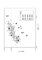
各実施例・比較例の評価結果を表1に示す。また、各実施例・比較例および比較例1と同条件で成長した一般的なウェハのそれぞれについて、GaAs結晶中のSi濃度とGaAs結晶中のB濃度との関係を図4に示す。
(Evaluation results)
Table 1 shows the evaluation results of the examples and comparative examples. FIG. 4 shows the relationship between the Si concentration in the GaAs crystal and the B concentration in the GaAs crystal for each of the general wafers grown under the same conditions as in each of the examples / comparative examples and comparative example 1.

実施例1では、Seed側、Middle位置、Tail側のいずれのウェハもEPDが低く、特にTail側ではキャリア濃度が2×1018cm−3より高く、EPDの最大値が500cm−2以下であるウェハを得ることができた。また、実施例2ではより広い領域のウェハ(Middle位置およびTail側)で同様のウェハを得ることができた。実施例3でもMiddle位置で、同様のウェハを得ることができた。 In Example 1, the EPD is low in any of the wafers on the Seed side, Middle position, and Tail side. In particular, on the Tail side, the carrier concentration is higher than 2 × 10 18 cm −3 and the maximum value of EPD is 500 cm −2 or less. A wafer could be obtained. In Example 2, a similar wafer could be obtained with a wider area wafer (middle position and tail side). In Example 3, a similar wafer could be obtained at the Middle position.
一方、比較例1では、Tail側ウェハのキャリア濃度は2×1018cm−3より高くなったものの、EPDの最大値1500cm−2以下となり、高いキャリア濃度を有し、かつ、結晶性の良いウェハを得ることはできなかった。また、図4から視覚的に明らかなように、比較例1ではSi濃度が高いTail側ではB濃度が6×1018cm−3を超えている。このため、スカムの発生を十分に抑制することができず、結晶性が悪いものと考えられる。比較例2も同様であった。 On the other hand, in Comparative Example 1, although the carrier concentration of the tail-side wafer is higher than 2 × 10 18 cm −3 , the EPD maximum value is 1500 cm −2 or less, and has a high carrier concentration and good crystallinity. A wafer could not be obtained. Further, as is apparent from FIG. 4, in Comparative Example 1, the B concentration exceeds 6 × 10 18 cm −3 on the tail side where the Si concentration is high. For this reason, generation | occurrence | production of a scum cannot fully be suppressed but it is thought that crystallinity is bad. The same was true for Comparative Example 2.
また、実施例3ではTail側でEPDの最大値が実施例1よりも大幅に増加した。よって、石英板を用いる場合、結晶成長中に液体封止剤の撹拌を行うことが好ましいことがわかった。 Further, in Example 3, the maximum EPD value on the Tail side was significantly increased compared to Example 1. Therefore, it was found that when a quartz plate is used, it is preferable to stir the liquid sealant during crystal growth.
ここで、実施例1と比較例2の結果より、石英板がB2O3に溶解するタイミングについて考察する。実施例1ではGaAs中にSi200質量ppm分のSi結晶をチャージした結果、seed側でキャリア濃度1.1×1018cm−3となり、比較例2ではSi280質量ppm分のSi結晶をチャージした結果、seed側でキャリア濃度1.2×1018cm−3となっている。比較例2の方のチャージ量が多いにも関わらずキャリア濃度の差はほとんどなく、seed側(結晶成長開始段階)において、比較例2より実施例1の方が、チャージしたSi結晶がキャリアとして結晶中に取り込まれている割合が高いことがわかる。これは、結晶成長開始段階より前、つまり加熱中にB2O3が軟化し、その後GaAsが融解していく過程で、B2O3中にSiO2として取り込まれたSiの量が少ないことを意味する。加熱中も反応式(1)の平衡を左辺側にシフトさせる減少が起きているということであり、固体の石英板により軟化したB2O3とGaAs原料との接触が抑制され、その後、加熱中の段階で石英板が軟化したB2O3に溶けてB2O3中に高濃度SiO2領域が出てきていると推測される。すなわち、加熱中の初期に一時的であれ石英板が固体として存在することで、軟化したB2O3と未溶融のGaAs原料との不要な接触を抑制し、結晶成長開始段階のGaAs融液に含まれるSiおよびBの量をより好ましい範囲にすることできる。 Here, based on the results of Example 1 and Comparative Example 2, the timing at which the quartz plate is dissolved in B 2 O 3 will be considered. In Example 1, as a result of charging Si crystal of Si 200 mass ppm into GaAs, the carrier concentration was 1.1 × 10 18 cm −3 on the seed side, and in Comparative Example 2, the Si crystal of Si 280 mass ppm was charged. The carrier concentration is 1.2 × 10 18 cm −3 on the seed side. Although the charge amount of Comparative Example 2 is larger, there is almost no difference in carrier concentration, and on the seed side (crystal growth start stage), in Example 1, the charged Si crystal is used as a carrier than Comparative Example 2. It can be seen that the ratio of incorporation into the crystal is high. This is because the amount of Si taken in as SiO 2 in B 2 O 3 is small before B 2 O 3 softens and then melts after heating, before the crystal growth start stage. Means. This means that there is a decrease that shifts the equilibrium of the reaction formula (1) to the left side during the heating, and the contact between the B 2 O 3 softened by the solid quartz plate and the GaAs raw material is suppressed, and then the heating is performed. high density SiO 2 region is assumed that came out quartz plate melts the B 2 O 3 softened in B 2 O 3 at a stage during. That is, the presence of the quartz plate as a solid even temporarily during heating suppresses unnecessary contact between the softened B 2 O 3 and the unmelted GaAs raw material, and the GaAs melt at the beginning of crystal growth. The amount of Si and B contained in can be made a more preferable range.
さらに、実施例1、比較例1、比較例2の結果より、原料溶融後のB2O3下層の高濃度SiO2層について考察する。比較例1ではB2O3中のSi濃度は平均で1.6質量%であり、比較例2ではB2O3中のSi濃度は平均で4.0質量%である。図4で同程度のGaAs融液中のSi濃度に対するGaAs融液中のB濃度を見ると、比較例1に比べて比較例2の方がややB濃度が低い傾向にある。つまり、B2O3中のSi濃度が高いほど、GaAs中のB濃度が低くなる傾向があるが、比較例1と比較例2のように、B2O3中のSi濃度が1.6質量%から4.0質量%と2.5倍に増えても、GaAs中のB濃度はやや低い程度にとどまる。これに対し、実施例1ではB2O3中のSi濃度は、石英板中のSi量を加えた値で5.2質量%と比較例1に対して3.25倍であるが、図4からわかるように、GaAs中のB濃度の低下傾向は比較例1と比較例2の差以上に顕著である。これは、実施例1で投入した石英板がB2O3中に均一に溶解しているのではなく、B2O3下層に5質量%よりも高い濃度の高濃度SiO2層として存在していることを示唆している。さらに、実施例1ではGaAs結晶成長後に、封止剤をアルコール溶解した後に1.5gの石英を回収しているが、原料溶融時点ではこの1.5gの石英もB2O3中で溶解し、高濃度SiO2層の形成に寄与していた可能性が高い。 Further, based on the results of Example 1, Comparative Example 1, and Comparative Example 2, the high-concentration SiO 2 layer of the B 2 O 3 lower layer after raw material melting will be considered. In Comparative Example 1, the Si concentration in B 2 O 3 is 1.6% by mass on average, and in Comparative Example 2, the Si concentration in B 2 O 3 is 4.0% by mass on average. When looking at the B concentration in the GaAs melt with respect to the Si concentration in the GaAs melt of the same degree in FIG. 4, the comparative example 2 tends to have a slightly lower B concentration than the comparative example 1. That is, the higher the Si concentration in B 2 O 3 , the lower the B concentration in GaAs tends to be. However, as in Comparative Example 1 and Comparative Example 2, the Si concentration in B 2 O 3 is 1.6. Even if the mass percentage is increased by 2.5 times from 4.0 mass% to 4.0 mass%, the B concentration in GaAs remains slightly low. In contrast, in Example 1, the Si concentration in B 2 O 3 is 5.2% by mass, which is the value obtained by adding the amount of Si in the quartz plate, which is 3.25 times that in Comparative Example 1. As can be seen from FIG. 4, the tendency of the B concentration in GaAs to decrease is more remarkable than the difference between Comparative Example 1 and Comparative Example 2. This is a quartz plate was placed in Example 1 B 2 O 3 rather than being homogeneously dissolved in, B 2 O 3 exists as a lower layer in a high concentration layer of SiO 2 concentration higher than 5 wt% Suggests that Further, in Example 1, 1.5 g of quartz was recovered after the GaAs crystal was grown and the sealing agent was dissolved in alcohol, but at the time of melting the raw material, 1.5 g of quartz was also dissolved in B 2 O 3. The possibility of contributing to the formation of the high-concentration SiO 2 layer is high.
図4から明らかなように、実施例は比較例および従来の一般的なウェハよりも、Si濃度が高くてもB濃度を低く抑えることができている。そのため、高いキャリア濃度を有し、かつ、高い結晶性を有するGaAs単結晶を製造することが可能となったものと思われる。 As can be seen from FIG. 4, in the example, the B concentration can be kept lower than the comparative example and the conventional general wafer even if the Si concentration is high. Therefore, it seems that it became possible to produce a GaAs single crystal having a high carrier concentration and high crystallinity.
本発明によれば、高いキャリア濃度を有し、かつ、高い結晶性を有するGaAs単結晶を製造することが可能となった。そして、このGaAs単結晶から、高いキャリア濃度を有しかつ高い結晶性を有するGaAs単結晶ウェハを得ることが可能となった。 According to the present invention, a GaAs single crystal having a high carrier concentration and high crystallinity can be produced. From this GaAs single crystal, a GaAs single crystal wafer having a high carrier concentration and high crystallinity can be obtained.
1 下部ロッド
2 上部ロッド
3 るつぼ収納容器
4 るつぼ
5 気密容器
6A,6B シールリング
7 撹拌板
8 断熱材
9 ヒーター
10 種結晶
12 Si原料
14 GaAs原料
15 融液部(GaAs融液)
16 石英板(固体の二酸化ケイ素)
17 SiO2高濃度層
18 酸化ホウ素原料
19 液体酸化ホウ素(液体封止剤)
20 固化部(SiドープGaAs単結晶)
DESCRIPTION OF SYMBOLS 1 Lower rod 2 Upper rod 3
16 Quartz plate (solid silicon dioxide)
17 SiO 2 high-concentration layer 18 Boron oxide
20 Solidified part (Si-doped GaAs single crystal)
すなわち、上記課題に鑑み、本発明の要旨構成は以下の通りである。
(1)種結晶、不純物となるSi原料およびGaAs原料、固体の二酸化ケイ素、ならびに予めSiO 2 が添加された酸化ホウ素原料をるつぼ内に収容した状態で縦型ボート法を行い、GaAs単結晶を成長させるにあたり、前記酸化ホウ素原料中のSiO 2 のSi量および前記固体の二酸化ケイ素中のSi量の合計が、前記酸化ホウ素原料の質量に対して5質量%を超えることを特徴とするGaAs単結晶の製造方法。
That is, in view of the above problems, the gist of the present invention is as follows.
(1) A vertical boat method is carried out in a state where a seed crystal, Si raw material and GaAs raw material to be impurities, solid silicon dioxide, and a boron oxide raw material to which SiO 2 has been added in advance are housed in a crucible. In the growth, the total amount of Si in SiO 2 in the boron oxide raw material and Si in the solid silicon dioxide exceeds 5% by mass with respect to the mass of the boron oxide raw material. Crystal production method.
(2)前記固体の二酸化ケイ素を前記GaAs原料と前記酸化ホウ素原料との間に配置する上記(1)に記載のGaAs単結晶の製造方法。 (2) The method for producing a GaAs single crystal according to (1), wherein the solid silicon dioxide is disposed between the GaAs raw material and the boron oxide raw material.
(4)キャリア濃度が2×1018cm−3より高く、エッチピット密度の最大値が500cm−2以下であり、B濃度が1.9×10 18 〜6×10 18 cm −3 であり、Si濃度が4.3×10 18 〜6.2×10 18 cm −3 であることを特徴とするSiドープGaAs単結晶ウェハ。
(4) higher than the carrier concentration of 2 × 10 18 cm -3, the maximum value of etch pit density is 500 cm -2 Ri der less, B concentration be 1.9 × 10 18 ~6 × 10 18 cm -3 , Si-doped GaAs single crystal wafer having Si concentration is characterized 4.3 × 10 18 ~6.2 × 10 18 cm -3 der Rukoto.
Claims (4)
前記酸化ホウ素原料中のSiO2のSi量および前記固体の二酸化ケイ素中のSi量の合計が、前記酸化ホウ素原料の質量に対して5質量%を超える請求項1に記載のGaAs単結晶の製造方法。 In the boron oxide raw material, SiO 2 is added in advance,
2. The production of a GaAs single crystal according to claim 1, wherein the total amount of Si in SiO 2 in the boron oxide raw material and the amount of Si in the solid silicon dioxide exceeds 5% by mass with respect to the mass of the boron oxide raw material. Method.
A Si-doped GaAs single crystal wafer having a carrier concentration higher than 2 × 10 18 cm −3 and a maximum etch pit density of 500 cm −2 or less.
Priority Applications (9)
| Application Number | Priority Date | Filing Date | Title |
|---|---|---|---|
| JP2011117420A JP5433632B2 (en) | 2011-05-25 | 2011-05-25 | GaAs single crystal manufacturing method and GaAs single crystal wafer |
| DE112012002217.3T DE112012002217B4 (en) | 2011-05-25 | 2012-05-16 | A method for producing a GaAs single crystal and GaAs single crystal wafers |
| PCT/JP2012/003204 WO2012160781A1 (en) | 2011-05-25 | 2012-05-16 | Method for producing gaas single crystal and gaas single crystal wafer |
| US14/122,042 US9469916B2 (en) | 2011-05-25 | 2012-05-16 | Method of producing GaAs single crystal and GaAs single crystal wafer |
| SG2013087192A SG195154A1 (en) | 2011-05-25 | 2012-05-16 | Method for producing gaas single crystal and gaas single crystal wafer |
| CN201280036835.1A CN103703172B (en) | 2011-05-25 | 2012-05-16 | The manufacture method of GaAs monocrystalline and GaAs single-crystal wafer |
| KR1020137034356A KR101857612B1 (en) | 2011-05-25 | 2012-05-16 | Method for producing gaas single crystal and gaas single crystal wafer |
| TW105126455A TWI572752B (en) | 2011-05-25 | 2012-05-21 | GaAs single crystal wafer |
| TW101117973A TWI582277B (en) | 2011-05-25 | 2012-05-21 | GaAs single crystal and GaAs single crystal wafer |
Applications Claiming Priority (1)
| Application Number | Priority Date | Filing Date | Title |
|---|---|---|---|
| JP2011117420A JP5433632B2 (en) | 2011-05-25 | 2011-05-25 | GaAs single crystal manufacturing method and GaAs single crystal wafer |
Publications (2)
| Publication Number | Publication Date |
|---|---|
| JP2012246156A true JP2012246156A (en) | 2012-12-13 |
| JP5433632B2 JP5433632B2 (en) | 2014-03-05 |
Family
ID=47216874
Family Applications (1)
| Application Number | Title | Priority Date | Filing Date |
|---|---|---|---|
| JP2011117420A Active JP5433632B2 (en) | 2011-05-25 | 2011-05-25 | GaAs single crystal manufacturing method and GaAs single crystal wafer |
Country Status (8)
| Country | Link |
|---|---|
| US (1) | US9469916B2 (en) |
| JP (1) | JP5433632B2 (en) |
| KR (1) | KR101857612B1 (en) |
| CN (1) | CN103703172B (en) |
| DE (1) | DE112012002217B4 (en) |
| SG (1) | SG195154A1 (en) |
| TW (2) | TWI572752B (en) |
| WO (1) | WO2012160781A1 (en) |
Cited By (5)
| Publication number | Priority date | Publication date | Assignee | Title |
|---|---|---|---|---|
| JP6394838B1 (en) * | 2017-07-04 | 2018-09-26 | 住友電気工業株式会社 | Gallium arsenide crystal and gallium arsenide crystal substrate |
| US10676812B2 (en) * | 2015-08-21 | 2020-06-09 | Flisom Ag | Evaporation source |
| WO2023054202A1 (en) * | 2021-09-29 | 2023-04-06 | Dowaエレクトロニクス株式会社 | Gaas wafer, gaas wafer group, and method for producing gaas ingot |
| JP7256326B1 (en) | 2021-09-29 | 2023-04-11 | Dowaエレクトロニクス株式会社 | GaAs wafer, GaAs wafer group, and method for manufacturing GaAs ingot |
| WO2024062991A1 (en) * | 2022-09-21 | 2024-03-28 | Dowaエレクトロニクス株式会社 | Method for producing gaas ingot, and gaas ingot |
Families Citing this family (2)
| Publication number | Priority date | Publication date | Assignee | Title |
|---|---|---|---|---|
| KR101956754B1 (en) | 2017-08-01 | 2019-03-11 | 한국과학기술연구원 | DEVICE FOR SINGLE CRYSTAL GROWTH OF GaAs |
| JP6798637B1 (en) * | 2019-07-10 | 2020-12-09 | 住友電気工業株式会社 | Gallium arsenide single crystal substrate |
Citations (5)
| Publication number | Priority date | Publication date | Assignee | Title |
|---|---|---|---|---|
| JPH0357079B2 (en) * | 1986-12-27 | 1991-08-30 | ||
| JPH08151290A (en) * | 1994-09-28 | 1996-06-11 | Sumitomo Electric Ind Ltd | Method for growing single crystal of compound semiconductor |
| JPH10259100A (en) * | 1997-03-18 | 1998-09-29 | Japan Energy Corp | Production of garium-arsenic single crystal |
| JPH10279398A (en) * | 1997-03-31 | 1998-10-20 | Dowa Mining Co Ltd | Gallium arsenide single crystal and its production |
| JP2000086398A (en) * | 1998-07-07 | 2000-03-28 | Mitsubishi Chemicals Corp | P type gaas single crystal and its production |
Family Cites Families (8)
| Publication number | Priority date | Publication date | Assignee | Title |
|---|---|---|---|---|
| JPH06219900A (en) | 1993-01-28 | 1994-08-09 | Dowa Mining Co Ltd | Production of si-doped n-type gallium arsenide single crystal |
| US5612014A (en) * | 1994-08-10 | 1997-03-18 | Sumitomo Electric Industries, Ltd. | Compound semiconductor crystal |
| JP3260568B2 (en) * | 1994-10-31 | 2002-02-25 | 株式会社神戸製鋼所 | Crucible for compound semiconductor production |
| US6325849B1 (en) * | 1998-07-07 | 2001-12-04 | Mitsubishi Chemical Corporation | P-type gaas single crystal and method for manufacturing the same |
| JP4168115B2 (en) | 1998-10-01 | 2008-10-22 | Dowaエレクトロニクス株式会社 | Method for producing Si-doped GaAs single crystal |
| US6896729B2 (en) * | 2001-07-05 | 2005-05-24 | Axt, Inc. | Method and apparatus for growing semiconductor crystals with a rigid support with carbon doping and resistivity control and thermal gradient control |
| JP5111104B2 (en) * | 2005-03-31 | 2012-12-26 | Dowaエレクトロニクス株式会社 | Si-doped GaAs single crystal ingot and method for producing the same |
| US8299351B2 (en) * | 2009-02-24 | 2012-10-30 | Hong Kong Applied Science And Technology Research Institute Co., Ltd. | Epitaxial growth of III-V compounds on (111) silicon for solar cells |
-
2011
- 2011-05-25 JP JP2011117420A patent/JP5433632B2/en active Active
-
2012
- 2012-05-16 KR KR1020137034356A patent/KR101857612B1/en active IP Right Grant
- 2012-05-16 WO PCT/JP2012/003204 patent/WO2012160781A1/en active Application Filing
- 2012-05-16 US US14/122,042 patent/US9469916B2/en active Active
- 2012-05-16 DE DE112012002217.3T patent/DE112012002217B4/en active Active
- 2012-05-16 SG SG2013087192A patent/SG195154A1/en unknown
- 2012-05-16 CN CN201280036835.1A patent/CN103703172B/en active Active
- 2012-05-21 TW TW105126455A patent/TWI572752B/en active
- 2012-05-21 TW TW101117973A patent/TWI582277B/en active
Patent Citations (5)
| Publication number | Priority date | Publication date | Assignee | Title |
|---|---|---|---|---|
| JPH0357079B2 (en) * | 1986-12-27 | 1991-08-30 | ||
| JPH08151290A (en) * | 1994-09-28 | 1996-06-11 | Sumitomo Electric Ind Ltd | Method for growing single crystal of compound semiconductor |
| JPH10259100A (en) * | 1997-03-18 | 1998-09-29 | Japan Energy Corp | Production of garium-arsenic single crystal |
| JPH10279398A (en) * | 1997-03-31 | 1998-10-20 | Dowa Mining Co Ltd | Gallium arsenide single crystal and its production |
| JP2000086398A (en) * | 1998-07-07 | 2000-03-28 | Mitsubishi Chemicals Corp | P type gaas single crystal and its production |
Cited By (8)
| Publication number | Priority date | Publication date | Assignee | Title |
|---|---|---|---|---|
| US10676812B2 (en) * | 2015-08-21 | 2020-06-09 | Flisom Ag | Evaporation source |
| JP6394838B1 (en) * | 2017-07-04 | 2018-09-26 | 住友電気工業株式会社 | Gallium arsenide crystal and gallium arsenide crystal substrate |
| WO2019008663A1 (en) * | 2017-07-04 | 2019-01-10 | 住友電気工業株式会社 | Gallium arsenide crystalline body and gallium arsenide crystal substrate |
| US10822722B2 (en) | 2017-07-04 | 2020-11-03 | Sumitomo Electric Industries, Ltd. | Gallium arsenide crystal body and gallium arsenide crystal substrate |
| WO2023054202A1 (en) * | 2021-09-29 | 2023-04-06 | Dowaエレクトロニクス株式会社 | Gaas wafer, gaas wafer group, and method for producing gaas ingot |
| JP7256326B1 (en) | 2021-09-29 | 2023-04-11 | Dowaエレクトロニクス株式会社 | GaAs wafer, GaAs wafer group, and method for manufacturing GaAs ingot |
| JP2023056483A (en) * | 2021-09-29 | 2023-04-19 | Dowaエレクトロニクス株式会社 | GaAs wafer, GaAs wafer group and method for manufacturing GaAs ingot |
| WO2024062991A1 (en) * | 2022-09-21 | 2024-03-28 | Dowaエレクトロニクス株式会社 | Method for producing gaas ingot, and gaas ingot |
Also Published As
| Publication number | Publication date |
|---|---|
| DE112012002217B4 (en) | 2018-03-01 |
| TW201250073A (en) | 2012-12-16 |
| DE112012002217T5 (en) | 2014-07-03 |
| TW201704569A (en) | 2017-02-01 |
| WO2012160781A1 (en) | 2012-11-29 |
| CN103703172A (en) | 2014-04-02 |
| TWI572752B (en) | 2017-03-01 |
| US9469916B2 (en) | 2016-10-18 |
| JP5433632B2 (en) | 2014-03-05 |
| KR20140044831A (en) | 2014-04-15 |
| US20140205527A1 (en) | 2014-07-24 |
| CN103703172B (en) | 2016-08-31 |
| SG195154A1 (en) | 2013-12-30 |
| TWI582277B (en) | 2017-05-11 |
| KR101857612B1 (en) | 2018-05-14 |
Similar Documents
| Publication | Publication Date | Title |
|---|---|---|
| JP5433632B2 (en) | GaAs single crystal manufacturing method and GaAs single crystal wafer | |
| EP1634981B1 (en) | Indium phosphide substrate, indium phosphide single crystal and process for producing them | |
| JP5216123B2 (en) | Si-doped GaAs single crystal ingot, method for producing the same, and Si-doped GaAs single crystal wafer produced from the Si-doped GaAs single crystal ingot | |
| TWI699464B (en) | Compound semiconductor and compound semiconductor single crystal manufacturing method | |
| JP7242757B2 (en) | GaAs ingot, GaAs ingot manufacturing method, and GaAs wafer | |
| JP4726138B2 (en) | Quartz glass crucible | |
| US20040187768A1 (en) | P-type GaAs single crystal and its production method | |
| TW200419015A (en) | Process for producing single crystal of compound semiconductor and crystal growing apparatus | |
| JP3818023B2 (en) | Method for producing GaAs single crystal | |
| JP2004217508A (en) | Si-DOPED GaAs SINGLE CRYSTAL INGOT, PRODUCTION METHOD THEREFOR, AND APPARATUS FOR PRODUCING COMPOUND SEMICONDUCTOR SINGLE CRYSTAL INGOT | |
| TW202413739A (en) | Manufacturing method of GaAs ingot and GaAs ingot | |
| JP2010030847A (en) | Production method of semiconductor single crystal | |
| JP4200690B2 (en) | GaAs wafer manufacturing method | |
| WO2024062991A1 (en) | Method for producing gaas ingot, and gaas ingot | |
| JP5429022B2 (en) | GaAs crystal and method for producing GaAs crystal | |
| JP2010030868A (en) | Production method of semiconductor single crystal | |
| JP2024045037A (en) | GaAs ingot manufacturing method and GaAs ingot | |
| JP2005350295A (en) | Semiconductor crystal and production method therefor | |
| JP2014094853A (en) | Method for manufacturing semiconductor single crystal of iii-v group compound, and semiconductor single crystal substrate of iii-v group compound | |
| JP2003176198A (en) | Method of manufacturing single crystal and single crystal ingot of compound semiconductor | |
| JP2016199416A (en) | Method for manufacturing sapphire single crystal | |
| JP2006089339A (en) | Method for manufacturing gallium phosphide single crystal | |
| JP2009208992A (en) | Method for manufacturing compound semiconductor single crystal |
Legal Events
| Date | Code | Title | Description |
|---|---|---|---|
| A521 | Request for written amendment filed |
Free format text: JAPANESE INTERMEDIATE CODE: A523 Effective date: 20120928 |
|
| A131 | Notification of reasons for refusal |
Free format text: JAPANESE INTERMEDIATE CODE: A131 Effective date: 20130205 |
|
| A521 | Request for written amendment filed |
Free format text: JAPANESE INTERMEDIATE CODE: A523 Effective date: 20130408 |
|
| A131 | Notification of reasons for refusal |
Free format text: JAPANESE INTERMEDIATE CODE: A131 Effective date: 20130507 |
|
| RD03 | Notification of appointment of power of attorney |
Free format text: JAPANESE INTERMEDIATE CODE: A7423 Effective date: 20130610 |
|
| A521 | Request for written amendment filed |
Free format text: JAPANESE INTERMEDIATE CODE: A523 Effective date: 20130708 |
|
| A131 | Notification of reasons for refusal |
Free format text: JAPANESE INTERMEDIATE CODE: A131 Effective date: 20130917 |
|
| A521 | Request for written amendment filed |
Free format text: JAPANESE INTERMEDIATE CODE: A523 Effective date: 20131101 |
|
| TRDD | Decision of grant or rejection written | ||
| A01 | Written decision to grant a patent or to grant a registration (utility model) |
Free format text: JAPANESE INTERMEDIATE CODE: A01 Effective date: 20131126 |
|
| A61 | First payment of annual fees (during grant procedure) |
Free format text: JAPANESE INTERMEDIATE CODE: A61 Effective date: 20131209 |
|
| R150 | Certificate of patent or registration of utility model |
Free format text: JAPANESE INTERMEDIATE CODE: R150 Ref document number: 5433632 Country of ref document: JP Free format text: JAPANESE INTERMEDIATE CODE: R150 |
|
| R250 | Receipt of annual fees |
Free format text: JAPANESE INTERMEDIATE CODE: R250 |
|
| R250 | Receipt of annual fees |
Free format text: JAPANESE INTERMEDIATE CODE: R250 |
|
| R250 | Receipt of annual fees |
Free format text: JAPANESE INTERMEDIATE CODE: R250 |
|
| R250 | Receipt of annual fees |
Free format text: JAPANESE INTERMEDIATE CODE: R250 |
|
| R250 | Receipt of annual fees |
Free format text: JAPANESE INTERMEDIATE CODE: R250 |
|
| R250 | Receipt of annual fees |
Free format text: JAPANESE INTERMEDIATE CODE: R250 |
|
| R250 | Receipt of annual fees |
Free format text: JAPANESE INTERMEDIATE CODE: R250 |
|
| R250 | Receipt of annual fees |
Free format text: JAPANESE INTERMEDIATE CODE: R250 |