JP2012243136A - Ladder programming tool - Google Patents
Ladder programming tool Download PDFInfo
- Publication number
- JP2012243136A JP2012243136A JP2011113585A JP2011113585A JP2012243136A JP 2012243136 A JP2012243136 A JP 2012243136A JP 2011113585 A JP2011113585 A JP 2011113585A JP 2011113585 A JP2011113585 A JP 2011113585A JP 2012243136 A JP2012243136 A JP 2012243136A
- Authority
- JP
- Japan
- Prior art keywords
- programmable controller
- circuit
- input
- personal computer
- ladder
- Prior art date
- Legal status (The legal status is an assumption and is not a legal conclusion. Google has not performed a legal analysis and makes no representation as to the accuracy of the status listed.)
- Pending
Links
Images
Landscapes
- Programmable Controllers (AREA)
Abstract
【課題】
従来は、プログラマブルコントローラに用いるシーケンスプログラムをデバッグする装置で、入出力接点の状態が時系列にどのように変化したかが分かるデバッガを提供するものがあった。
また、ラダープログラムを編集し直すことなく、着目した回路に限定して動作を確認することができるデバッグ装置およびプログラム確認方法があった。
【解決手段】
本発明は、プログラマブルコントローラのためのラダープログラミングツールにおいて、ユーザが作成したラダープログラムをデバッグするとき、ラダープログラムの変更を前記プログラマブルコントローラの記憶素子に記憶し、ユーザの要望に応じて、変更部分を前記パソコンの表示装置に遡って表示し、ラダープログラムの編集を行うことを特徴とする。
【選択図】 図1【Task】
Conventionally, there has been an apparatus for debugging a sequence program used for a programmable controller that provides a debugger that can understand how the state of an input / output contact changes in time series.
In addition, there has been a debugging device and a program checking method that can check the operation limited to a focused circuit without re-editing the ladder program.
[Solution]
When debugging a ladder program created by a user in a ladder programming tool for a programmable controller, the present invention stores the change of the ladder program in the storage element of the programmable controller, and changes the changed portion according to the user's request. The display is retroactively displayed on the display device of the personal computer, and the ladder program is edited.
[Selection] Figure 1
Description
本発明は、グラマブルコントローラのラダープログラミングツールにおいて、編集戻し機能を備えたラダープログラミングツールに関する。 The present invention relates to a ladder programming tool having an edit back function in a ladder programming tool for a grammable controller.
プログラマブルコントローラは、一般にCPUやメモリなどを内蔵したコントローラであり、センサやスイッチなどの入力信号を入力し、この入力信号のデータのプログラム演算を行い、この演算結果を出力データとして出力し、電磁弁、モータ又は表示灯などをON−OFFして制御するものである。 A programmable controller is generally a controller with a built-in CPU, memory, etc., which receives input signals from sensors, switches, etc., performs program operations on the data of these input signals, outputs the operation results as output data, and outputs a solenoid valve. In this case, the motor or indicator lamp is controlled by turning it on and off.
また、プログラマブルコントローラのプログラムは、一般にラダープログラムを使用する。ラダープログラムは、リレー回路を記号化したラダー図をベースにしてロジックを記述するプログラムで、入力条件と出力の関係を視覚的にイメージし易いプログラム言語である。このラダープログラムを作成するため、専用のエディタであるラダープログラミングツールを使ってプログラムを作成している。また、本発明の公知例として、特許文献1(特開2011−22838)及び特許文献2(特開平8−305418号公報)がある。 Further, a ladder program is generally used as the programmable controller program. A ladder program is a program that describes logic based on a ladder diagram that symbolizes a relay circuit, and is a program language that makes it easy to visually imagine the relationship between input conditions and outputs. In order to create this ladder program, the program is created using a ladder programming tool which is a dedicated editor. Further, as known examples of the present invention, there are Patent Document 1 (Japanese Patent Laid-Open No. 2011-22838) and Patent Document 2 (Japanese Patent Laid-Open No. 8-305418).
特許文献1には、ラダープログラムを編集し直すことなく、着目した回路に限定して動作を確認することができるデバッグ装置およびプログラム確認方法を実現することについて開示されている。 Patent Document 1 discloses realization of a debugging device and a program confirmation method that can confirm an operation limited to a focused circuit without re-editing a ladder program.
また、特許文献2には、プログラマブルコントローラに用いるシーケンスプログラムをデバッグする装置で、入出力接点の状態が時系列にどのように変化したかが分かるデバッガを提供することが記載されている。しかし、入出力接点を変更することは開示されていない。 Japanese Patent Application Laid-Open No. 2005-228561 describes that a device that debugs a sequence program used for a programmable controller provides a debugger that can understand how the state of input / output contacts changes in time series. However, changing the input / output contact is not disclosed.
本発明の目的は、実際にデバッグしたラダープログラムにおいて変更した箇所を記憶して格納し、ユーザは過去の変更した箇所を表示して選択して編集することができるプログラマブルコントローラのためのラダープログラミングツールを提供することにある。 An object of the present invention is to store and store a changed part in a ladder program that is actually debugged, and a ladder programming tool for a programmable controller that allows a user to display, select, and edit past changed parts. Is to provide.
本発明は、上記目的を達成するために、パソコンと、該パソコンと接続され、パソコンの内容を表示する表示装置と、前記パソコンとプログラマブルコントローラとを接続し、該プログラマブルコントローラは、中央演算装置、通信制御回路、記憶素子、入出力制御回路、入出力装置より構成され、前記パソコンと前記プログラマブルコントローラの中央演算装置は、前記通信制御回路を介して情報を送受信可能な構成で行うラダープログラミングツールにおいて、ユーザが作成したラダープログラムをデバッグするとき、ラダープログラムの変更を前記プログラマブルコントローラの記憶素子に記憶し、ユーザの要望に応じて、変更部分を前記パソコンの表示装置に遡って表示し、ラダープログラムの編集を行うことを特徴とする。 In order to achieve the above object, the present invention connects a personal computer, a display device connected to the personal computer, and displays the contents of the personal computer, the personal computer and the programmable controller, the programmable controller comprising a central processing unit, In a ladder programming tool configured by a communication control circuit, a storage element, an input / output control circuit, and an input / output device, the central processing unit of the personal computer and the programmable controller can transmit and receive information via the communication control circuit. When debugging the ladder program created by the user, the ladder program change is stored in the storage element of the programmable controller, and the changed part is displayed retrospectively on the display device of the personal computer according to the user's request. It is characterized by editing.
また、上記のラダープログラミングツールにおいて、ラダープログラムの変更部分はすべて前記プログラマブルコントローラの記憶素子に記憶することを特徴とする。 In the ladder programming tool, all the changed portions of the ladder program are stored in the storage element of the programmable controller.
本発明は、ユーザが実際に過去にデバッグしたラダープログラムを表示し、選択できるラダープログラミングツールを提供することができ、また、ユーザは過去にデバッグを行なった動作のラダープログラムを格納しているため、プログラマブルコントローラを使用した装置の動作の急な変更にも対応できる。
また、過去にデバッグを行なったラダープログラムを再利用できるため、そのラダープログラムのデバッグの時間短縮効果を得られる。
The present invention can provide a ladder programming tool that allows a user to display and select a ladder program actually debugged in the past, and the user stores a ladder program of an operation that has been debugged in the past. It can cope with a sudden change in the operation of the device using the programmable controller.
In addition, since a ladder program that has been debugged in the past can be reused, the debugging time of the ladder program can be shortened.
以下、本発明の実施の形態について図面を用いて説明する。 Hereinafter, embodiments of the present invention will be described with reference to the drawings.
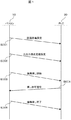
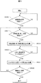
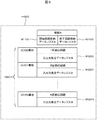
図1は、本発明の全体のシーケンスを示したものである。プログラマブルコントローラでは、プログラマブルコントローラ本体とパソコンを用いてユーザが作成したラダープログラムをプログラマブルコントローラで装置を動作させるためにそのラダープログラムの動作検証を行う。一般にこれをデバッグと呼んでいる。
本発明は、ラダープログラムのデバッグの際、修正を加え、何回もデバッグを行う。そのとき修正前に遡って入出力信号をユーザが選択できるプログラマブルコントローラのプログラミングツールを提供するものである。そのために、ユーザは、装置を動作させるため作成するラダープログラムを、その装置の機能毎に作成する。
FIG. 1 shows the entire sequence of the present invention. In the programmable controller, the ladder program created by the user using the programmable controller main body and the personal computer is verified in order to operate the apparatus using the programmable controller. This is generally called debugging.
According to the present invention, a ladder program is debugged many times by adding corrections. At this time, a programming tool for a programmable controller is provided that allows the user to select input / output signals retroactively. Therefore, the user creates a ladder program created for operating the device for each function of the device.
図1に示すように、パソコンP001とプログラマブルコントローラ(プログラマブルコントローラ01)間の全体の通信制御において、先ず、ユーザが作成するラダープログラムを機能単位で宣言する必要があり、パソコン側(P001)よりプログラマブルコントローラ側(プログラマブルコントローラ01)へ回路定義設定(ステップS001)を送信してプログラマブルコントローラ側(プログラマブルコントローラ01)に記憶する。
ここで、ラダープログラムを宣言するということは、ラダープログラムの範囲を設定するということである。また、回路とはラダープログラムのことをいう。
As shown in FIG. 1, in the overall communication control between the personal computer P001 and the programmable controller (programmable controller 01), first, it is necessary to declare a ladder program created by the user in units of functions, which is programmable from the personal computer side (P001). The circuit definition setting (step S001) is transmitted to the controller side (programmable controller 01) and stored in the programmable controller side (programmable controller 01).
Here, declaring a ladder program means setting the range of the ladder program. The circuit is a ladder program.
次に、ユーザが実際に入出力接点を変更すると、パソコン側ではその入出力接点をプログラマブルコントローラ側に連絡する必要があるため、パソコン側よりプログラマブルコントローラ側へ入出力接点定義設定(ステップS002)を送信する。
ユーザが前のラダープログラムに戻したい状況が発生したとすると、パソコン側より編集戻し開始信号(ステップS003)をプログラマブルコントローラ側に送信し、プログラマブルコントローラ側では過去のラダープログラムを戻す準備を行う。
そして、プログラマブルコントローラ側では過去のラダープログラムを戻す準備が整うと、プログラマブルコントローラ側よりパソコン側へ戻し許可信号(ステップS004)を送信する。
そして、戻し許可信号をパソコン側で受信すると、パソコン側では過去のラダープログラムをパソコンに接続された表示器の画面に表示して、編集戻し完了信号(ステップS005)をパソコン側よりプログラマブルコントローラ側へ送信する。
以上のステップによりパソコン側とプログラマブルコントローラ側の通信制御は完了する。
Next, when the user actually changes the input / output contact, since it is necessary on the personal computer side to communicate the input / output contact to the programmable controller side, input / output contact definition setting (step S002) is made from the personal computer side to the programmable controller side. Send.
If a situation occurs in which the user wants to return to the previous ladder program, an edit return start signal (step S003) is transmitted from the personal computer side to the programmable controller side, and the programmable controller side prepares to return the previous ladder program.
When the programmable controller side is ready to return the past ladder program, the programmable controller side transmits a return permission signal (step S004) to the personal computer side.
When the return permission signal is received on the personal computer side, the previous ladder program is displayed on the screen of the display device connected to the personal computer, and the edit return completion signal (step S005) is transferred from the personal computer side to the programmable controller side. Send.
Through the above steps, communication control between the personal computer side and the programmable controller side is completed.
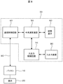
次に、本発明のハードウエア構成について、図8を用いて説明する。
図8において、10はパソコン、20はパソコン10に接続された表示装置、30はプログラマブルコントローラ,40は通信制御装置、50は中央演算装置(CPU)、60は記憶素子、70は入出力制御回路、80は入出力装置、90はパソコン10とプログラマブルコントローラ30とで通信を行う通信線である。
プログラマブルコントローラ30の中央演算装置50は、CPUで構成され、プログラマブルコントローラ内の記憶装置60、入出力装置70、通信制御回路40を制御している。通信線90はRS―232Cなどのシリアル通信で行っても良い。中央演算装置50は外部との入出力信号を制御し、入出力制御回路70は、入出力装置80と接続されている。
Next, the hardware configuration of the present invention will be described with reference to FIG.
In FIG. 8, 10 is a personal computer, 20 is a display device connected to the
The
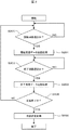
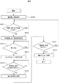
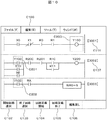
次に、図2を用いて、図1におけるパソコン側よりプログラマブルコントローラ側へ送信する回路定義設定(ステップS001)について説明する。
図2はパソコン側の回路定義設定のフローチャートである。
先ず、ユーザは、パソコン側でラダープログラムの機能単位の回路番号を宣言する。
そして、最初に図8におけるプログラマブルコントローラ側の中央演算装置(CPU)50は、図2において開始回路を選択する開始回路選択判定(ステップS200)を行う。開始回路の選択は、図10に示した回路定義開始ボタンC104を押して、回路番号C101を押すことにより実行される。
Next, the circuit definition setting (step S001) transmitted from the personal computer side in FIG. 1 to the programmable controller side will be described using FIG.
FIG. 2 is a flowchart of circuit definition setting on the personal computer side.
First, the user declares the circuit number of the ladder program functional unit on the personal computer side.
First, the central processing unit (CPU) 50 on the programmable controller side in FIG. 8 performs a start circuit selection determination (step S200) for selecting a start circuit in FIG. Selection of the start circuit is performed by pressing the circuit definition start button C104 shown in FIG. 10 and pressing the circuit number C101.
次に、図2における開始回路番号データを送信する処理(ステップS201)で、プログラマブルコントローラ側の通信制御回路40を経由してプログラマブルコントローラ側30へ送信する。次に、ラダープログラムの終了回路をユーザが宣言する。図2の終了回路データが選択されたかを図8における中央演算装置(CPU)50は終了回路選択判定(ステップS202)を実行する。そして、終了回路が選択されると、終了回路データを終了回路データ送信処理(ステップS203)にて、通信制御回路40を経由してプログラマブルコントローラ側へ送信する。終了回路の選択は、図10に示す回路定義終了ボタンC105を押して、回路番号C101を押して実行される。
なお、上記の終了回路データ送信処理(ステップS203)は、通信線90を経由してプログラマブルコントローラ側の通信制御回路40で終了回路データが受信処理されて、中央演算そうし(CPU)50にて記憶素子60に終了回路データを記憶する。そして、この一連の回路定義かが完了したことを定義終了判定(ステップS205)にて判定し、定義終了なら回路定義処理(ステップS206)を実行してプログラマブルコントローラ側へ送信する。
Next, in the process of transmitting start circuit number data in FIG. 2 (step S201), the data is transmitted to the
In the end circuit data transmission process (step S203) described above, the end circuit data is received and processed by the
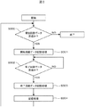
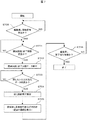
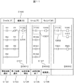
次に、図3を用いて、プログラマブルコントローラ側の回路定義設定について説明する。
図3において、中央演算装置(CPU)40で、先ず開始回路データを受信したかを判断する(ステップS300)。受信していなければこの処理自体を終了し、受信していれば、次に開始回路データを記憶する処理を実行する(ステップS301)。開始回路データ記憶処理において、図9に示す記憶素子内のデータ保管構造で、開始回路データを開始回路格納データレジスタM100に書き込む。次に、パソコン側より通信制御回路40経由で送信された終了回路データを受信したかを判断する(ステップS302)。終了回路データが受信されたら、図9に示すデータ保管構造で、終了回路格納データレジスタM102に終了回路データ記憶処理(ステップS303)を実行して書き込まれる。そして、その後、中央演算装置(CPU)40は、記憶処理(ステップS304)を実行し、記憶素子60内のアドレスポインタM100の0000番地のアドレスポインタ1を書き込む。
この操作は、図6に説明する変更回路をこの記憶素子に書き込むために必要な記憶素子内のアドレスを指し示す必要があるために利用する。
Next, the circuit definition setting on the programmable controller side will be described with reference to FIG.
In FIG. 3, the central processing unit (CPU) 40 first determines whether start circuit data has been received (step S300). If it has not been received, the process itself is terminated. If it has been received, a process for storing start circuit data is executed (step S301). In the start circuit data storage process, the start circuit data is written into the start circuit storage data register M100 with the data storage structure in the storage element shown in FIG. Next, it is determined whether the end circuit data transmitted from the personal computer side via the
This operation is used because the change circuit described in FIG. 6 needs to indicate an address in the storage element necessary for writing to the storage element.
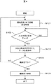
次に、図4を用いて、パソコン側での入出力接点の変更をプログラマブルコントローラ側に送信するフローチャートを説明する。
図4において、先ず、図10に示す開始回路番号C101を選択してから、開始回路選択ボタンC102を押す。そしてその後、終了回路番号C107を選択して、終了回路選択ボタンC103を押すと、開始回路番号データと終了回路番号データが、開始回路/終了回路送信処理(ステップS403)を実行し、パソコン側よりプログラマブルコントローラ側に送信される。
次に、ユーザが入出力接点を変更したかをチェック(ステップS404)する。
図10において、例えば、出力コイルの出力接点マークC200をY100からY200に変更すると、その接点であるC201とC202もY200に変わる。
この変更した入出力接点データは、入出力接点を変更されたデータ送信処理(ステップS403)を実行し、プログラマブルコントローラ側へ送信する。
そこで、ユーザが編集を完了するときは、もう一度図10の編集ボタンC100を押す。編集ボタンC100が押されると、編集完了が判断され(ステップS404)、編集完了信号がプログラマブルコントローラ側に送信され(ステップS405)、終了となる。
また、編集が完了していないときは、ユーザがまだ変更したい回路データがあるので、変更対象機能番号データの処理(ステップS401)へ戻る。
Next, a flowchart for transmitting the change of the input / output contact on the personal computer side to the programmable controller side will be described with reference to FIG.
In FIG. 4, first, the start circuit number C101 shown in FIG. 10 is selected, and then the start circuit selection button C102 is pressed. After that, when the end circuit number C107 is selected and the end circuit selection button C103 is pressed, the start circuit number data and the end circuit number data execute the start circuit / end circuit transmission process (step S403), and from the personal computer side. Sent to the programmable controller side.
Next, it is checked whether the user has changed the input / output contact (step S404).
In FIG. 10, for example, when the output contact mark C200 of the output coil is changed from Y100 to Y200, the contacts C201 and C202 also change to Y200.
The changed input / output contact data is transmitted to the programmable controller side by executing a data transmission process (step S403) in which the input / output contact is changed.
Therefore, when the user completes editing, the user presses the edit button C100 in FIG. 10 again. When the edit button C100 is pressed, editing completion is determined (step S404), an editing completion signal is transmitted to the programmable controller side (step S405), and the process ends.
If the editing is not completed, there is circuit data that the user still wants to change, and the process returns to the process of the function number data to be changed (step S401).
次に、プログラマブルコントローラ側において、変更された入出力接点を判定、受信し、記憶素子60に書き込むフローチャートを説明する。
図5において、先ず、パソコン側より送信された編集開始信号を受信したかを判断する(ステップS500)。編集開始信号を受信すると、次にプログラマブルコントローラ側の中央演算装置(CPU)50は、パソコン側より送信された開始回路番号データと終了回路番号データを受信したかを判断する(ステップS501)。開始回路番号データと終了回路番号データを受信すると、図3に示すフローチャートで登録した開始回路格納レジスタM100と、終了回路格納レジスタM102と同じ記憶素子60内のエリアを割り出し、開始回路/終了回路書き込み処理を中央演算装置(CPU)40で実行する(ステップS502)。次に、変更された入出力接点の変更データを受信し、判断する(ステップS503)。そして、1回前の変更入出力接点として、図9に示す記憶素子60の入出力接点データレジスタM200に、入出力接点変更データ書き込み処理を実行する(ステップS500)ことにより書き込まれる。
また、2回目からの記憶は、同様に記憶素子60内のアドレスポインタM0001の0001番地に1を書き込むと、入出力接点データレジスタM201に変更した入出力接点が書き込まれる。
同様に、n回目も記憶素子60内のアドレスポインタM001の000n番地に1を書き込むと、入出力接点データレジスタM20nに変更した入出力接点が書き込まれる。
Next, a flowchart for determining, receiving, and writing to the
In FIG. 5, first, it is determined whether an edit start signal transmitted from the personal computer side has been received (step S500). When the edit start signal is received, the central processing unit (CPU) 50 on the programmable controller side next determines whether the start circuit number data and the end circuit number data transmitted from the personal computer side have been received (step S501). When the start circuit number data and end circuit number data are received, the start circuit storage register M100 registered in the flowchart shown in FIG. 3 and the same area in the
Similarly, in the second storage, when 1 is written to the
Similarly, when 1 is written to address 000n of the address pointer M001 in the
次に、パソコン側より送信された編集完了信号を受信したかを判断する(ステップS505)。編集完了信号が受信されたら、一連の入出力接点の変更は終了する。編集完了信号が受信されなかったら、ユーザはまだ変更が発生するので開始回路番号データと終了回路番号データを受信し、判断するステップS501に戻り、動作を継続する。
以上のフローチャートで過去に変更した入出力接点がプログラマブルコントローラの記憶素子60に記憶される。
Next, it is determined whether an editing completion signal transmitted from the personal computer side has been received (step S505). When the edit completion signal is received, the series of input / output contact changes is completed. If the edit completion signal is not received, the user still receives a change, so the user receives the start circuit number data and the end circuit number data, returns to the determination step S501, and continues the operation.
The input / output contact changed in the past in the above flowchart is stored in the
次に、パソコン側での編集戻しについて、図6を用いて説明する。
図6は、今まで記憶してきた過去の入出力接点をユーザの要望により編集戻しをプログラマブルコントローラ側に送信するフローチャートである。
図10における編集戻しボタンC106を押すと、先ず、編集戻し開始信号がパソコン側よりプログラマブルコントローラ側に対して送信される(ステップS600)。これは、これまで変更などを行った過去の回路に編集を戻すことを宣言することである。
Next, editing back on the personal computer side will be described with reference to FIG.
FIG. 6 is a flowchart for sending the edit-back of past input / output contacts stored so far to the programmable controller side according to the user's request.
When the edit return button C106 in FIG. 10 is pressed, first, an edit return start signal is transmitted from the personal computer side to the programmable controller side (step S600). This is to declare that editing is to be returned to the past circuit that has been changed so far.
次に、図10における開始回路番号C101を押して開始回路選択ボタンC102を押す。その後、終了回路番号C107を押して、終了回路選択ボタンC103を押すと、開始回路番号データと終了回路番号データが入力されたかを判断する(ステップS601)。入力されると、開始回路データと終了回路データを、開始回路/終了回路送信処理を実行することでプログラマブルコントローラ側へ送信処理される(ステップS602)。
次に、図10における編集戻しボタンC106を押すと、戻し判定で判断される(ステップS603)。その後、入出力接点データ送信処理(ステップS604)において、図9に示す記憶素子60内のアドレスポインタM001が1の行の入出力接点データレジスタM200の入出力接点データをプログラマブルコントローラ側へ送信する。
次に、プログラマブルコントローラ側より変更戻し許可信号が受信されたかを変更戻し表示許可信号を受信したかを判断する(ステップS605)。受信していると、過去表示戻し処理を実行する(ステップS606)。すなわち、変更した入出力接点を遡って表示する。この場合、回路番号001から002の入出力接点マークC200とC201がY200よりY100に戻したということになる。しかし、回路番号002の入出力接点はY200のままである。これは回路選択をしていないためである。
以上のことより、ユーザは過去にデバッグしたラダープログラムを選択することができる。ユーザからの編集戻し操作が終了したかを判断する(ステップS607)。これは、図10に示す編集ボタンC106を押すと、編集終了となり、編集戻し完了処理を実行(ステップS608)し、プログラマブルコントローラ側に編集戻し完了信号を送信する。編集戻しが完了していなければ、編集戻しを実行していると判断し、ステップS601へ戻る。
Next, the start circuit number C101 in FIG. 10 is pressed and the start circuit selection button C102 is pressed. Thereafter, when the end circuit number C107 is pressed and the end circuit selection button C103 is pressed, it is determined whether start circuit number data and end circuit number data are input (step S601). When input, the start circuit data and the end circuit data are transmitted to the programmable controller side by executing the start circuit / end circuit transmission process (step S602).
Next, when the edit return button C106 in FIG. 10 is pressed, determination is made by return determination (step S603). Thereafter, in the input / output contact data transmission process (step S604), the input / output contact data of the input / output contact data register M200 in the row in which the address pointer M001 in the
Next, it is determined whether or not a change return permission signal has been received from the programmable controller side (step S605). If received, the past display return process is executed (step S606). That is, the changed input / output contact is displayed retrospectively. In this case, the input / output contact marks C200 and C201 having the circuit numbers 001 to 002 are returned from Y200 to Y100. However, the input / output contact of the circuit number 002 remains Y200. This is because the circuit is not selected.
From the above, the user can select a ladder program debugged in the past. It is determined whether the editing return operation from the user is completed (step S607). When the edit button C106 shown in FIG. 10 is pressed, editing is completed, editing return completion processing is executed (step S608), and an editing return completion signal is transmitted to the programmable controller side. If the edit return is not completed, it is determined that the edit return is being executed, and the process returns to step S601.
次に、図7を用いてプログラマブルコントローラ側での編集戻しの処理について説明する。
図7は、過去の入出力接点をユーザの要望により戻すプログラマブルコントローラ側のフローチャートである。
先ず、通信制御回路40で受信し、編集戻し開始信号が受信されたかを中央演算装置(CPU)50で判断する(ステップS700)。編集戻し開始信号が受信されると、次に開始回路/終了回路を受信したかを判断する(ステップS701)。開始回路/終了回路が受信されると、中央演算装置(CPU)50は、開始回路/終了回路のデータ処理を実行(ステップS702)し、記憶素子60内の開始回路格納レジスタM100と終了回路格納レジスタM102と同じ列のデータを検知処理する。次に、戻したい入出力接点データを受信したかを判断する(ステップS703)。受信されると、中央演算装置(CPU)50は、記憶素子60内のアドレスポインタM001が1の行の入出力接点データレジスタM200の入出力接点データを戻し開路実行処理(ステップS704)を実行し、検索処理を行う。また、このステップS704の処理では、図8に示すプログラマブルコントローラ側内の中央演算装置(CPU)50は、入出力制御回路70を制御して変更した入出力接点で入出力装置80を動作させる。その後、変更戻し表示許可信号の送信処理(ステップS705)を実行し、パソコン側へ送信する。また、この処理では過去のラダープログラムの回路を表示する。そして、編集戻し完了信号を受信したら終了となる。受信していないとステップS700に戻る。
Next, the edit return process on the programmable controller side will be described with reference to FIG.
FIG. 7 is a flowchart on the programmable controller side for returning the past input / output contacts according to the user's request.
First, the central processing unit (CPU) 50 determines whether it has been received by the
図10は、ユーザが作成するラダープログラムを機能単位で記憶する回路定義開始ボタンC104と回路定義終了ボタンC105を備えている。
ここで、回路の定義を行い、そのデータをプログラマブルコントローラ側の記憶素子60に登録する。
次に、ユーザはデバッグに移る。その時、編集ボタンC100を押して、編集開始したい回路番号C101を選択して、開始回路選択ボタンC102を押す。
次に、編集の終わり回路番号C107を選択して、終了回路選択ボタンC103を押す。このような作業により、この例では回路番号1と回路番号2が編集できる回路に選択できる。
次に、変更したい入出力接点C200の内容をY100からY201に変更する。
ここで、変更した内容は、プログラマブルコントローラ側の記憶素子に記憶される。
次に、上記内容で過去にデバッグした状態に戻したい時が発生した場合、ユーザは編集戻しボタンC106を押すと、回路番号0001と回路番号0002が過去で使用していた入出力接点C200がY100、C201がY100となり過去の状態に戻すことができる。また、回路番号0003の入出力接点C202は変更されない。従って、各回路の機能単位での過去にデバッグを行ったラダープログラムを再利用できるため、そのラダープログラムのデバッグの時間短縮効果を得られ、過去にデバッグしたラダープログラムをユーザが選択できる。
FIG. 10 includes a circuit definition start button C104 and a circuit definition end button C105 for storing a ladder program created by the user in units of functions.
Here, the circuit is defined and the data is registered in the
Next, the user goes to debugging. At that time, the edit button C100 is pressed to select the circuit number C101 to start editing, and the start circuit selection button C102 is pressed.
Next, the edit end circuit number C107 is selected, and the end circuit selection button C103 is pressed. By such work, in this example, it is possible to select a circuit that can edit circuit numbers 1 and 2.
Next, the content of the input / output contact C200 to be changed is changed from Y100 to Y201.
Here, the changed content is stored in the storage element on the programmable controller side.
Next, when the user wants to return to the debugged state in the past, when the user presses the edit back button C106, the
また、図11に示すように、パソコン側の画面構成は縦長方向に表示することも可能である。画面の構成については、図10と同じなので説明は省略する。 Further, as shown in FIG. 11, the screen configuration on the personal computer side can be displayed in the portrait orientation. The screen configuration is the same as in FIG.
10‥パソコン 20‥表示装置 30‥プログラマブルコントローラ
40‥通信制御装置 50‥中央演算装置(CPU) 60‥記憶素子
70‥入出力制御回路 80‥入出力装置
M001‥アドレスポインタ
M100‥開始回路格納データレジスタ
M102‥終了回路格納データレジスタ
M200‥1回前の回路の入出力接点データレジスタ
M201‥2回前の回路の入出力接点データレジスタ
M20N‥n回前の回路の入出力接点データレジスタ
C100‥編集ボタン
C101‥回路番号
C102‥開始回路選択ボタン
C103‥終了回路選択ボタン
C104‥回路定義開始ボタン
C105‥回路定義終了ボタン
C106‥編集戻しボタン。
DESCRIPTION OF
Claims (2)
該パソコンと接続され、パソコンの内容を表示する表示装置と、
前記パソコンとプログラマブルコントローラとを接続し、
該プログラマブルコントローラは、中央演算装置、通信制御回路、記憶素子、入出力制御回路、入出力装置より構成され、
前記パソコンと前記プログラマブルコントローラの中央演算装置は、前記通信制御回路を介して情報を送受信可能な構成で行うラダープログラミングツールにおいて、
ユーザが作成したラダープログラムをデバッグするとき、ラダープログラムの変更を前記プログラマブルコントローラの記憶素子に記憶し、
ユーザの要望に応じて、変更部分を前記パソコンの表示装置に遡って表示し、ラダープログラムの編集を行うことを特徴とするラダープログラミングツール。 With a computer,
A display device connected to the personal computer and displaying the contents of the personal computer;
Connect the personal computer and the programmable controller,
The programmable controller includes a central processing unit, a communication control circuit, a storage element, an input / output control circuit, and an input / output device.
In the ladder programming tool, the central processing unit of the personal computer and the programmable controller is configured to transmit and receive information via the communication control circuit.
When debugging a ladder program created by a user, the change of the ladder program is stored in the storage element of the programmable controller,
A ladder programming tool characterized by displaying a changed part retroactively on the display device of the personal computer and editing a ladder program according to a user's request.
ラダープログラムの変更部分はすべて前記プログラマブルコントローラの記憶素子に記憶することを特徴とするラダープログラミングツール。 The ladder programming tool according to claim 1.
A ladder programming tool characterized in that all changed portions of a ladder program are stored in a storage element of the programmable controller.
Priority Applications (1)
| Application Number | Priority Date | Filing Date | Title |
|---|---|---|---|
| JP2011113585A JP2012243136A (en) | 2011-05-20 | 2011-05-20 | Ladder programming tool |
Applications Claiming Priority (1)
| Application Number | Priority Date | Filing Date | Title |
|---|---|---|---|
| JP2011113585A JP2012243136A (en) | 2011-05-20 | 2011-05-20 | Ladder programming tool |
Publications (1)
| Publication Number | Publication Date |
|---|---|
| JP2012243136A true JP2012243136A (en) | 2012-12-10 |
Family
ID=47464769
Family Applications (1)
| Application Number | Title | Priority Date | Filing Date |
|---|---|---|---|
| JP2011113585A Pending JP2012243136A (en) | 2011-05-20 | 2011-05-20 | Ladder programming tool |
Country Status (1)
| Country | Link |
|---|---|
| JP (1) | JP2012243136A (en) |
Cited By (1)
| Publication number | Priority date | Publication date | Assignee | Title |
|---|---|---|---|---|
| CN111158301A (en) * | 2018-11-07 | 2020-05-15 | 发那科株式会社 | Tracking device and programmable controller |
Citations (3)
| Publication number | Priority date | Publication date | Assignee | Title |
|---|---|---|---|---|
| JP2001142510A (en) * | 1999-11-11 | 2001-05-25 | Omron Corp | Controller system and programming tool and controller |
| JP2004021446A (en) * | 2002-06-14 | 2004-01-22 | Mitsubishi Electric Corp | Programmable controller system and programmable controller |
| JP2011022838A (en) * | 2009-07-16 | 2011-02-03 | Yokogawa Electric Corp | Debug device and ladder program verification method |
-
2011
- 2011-05-20 JP JP2011113585A patent/JP2012243136A/en active Pending
Patent Citations (3)
| Publication number | Priority date | Publication date | Assignee | Title |
|---|---|---|---|---|
| JP2001142510A (en) * | 1999-11-11 | 2001-05-25 | Omron Corp | Controller system and programming tool and controller |
| JP2004021446A (en) * | 2002-06-14 | 2004-01-22 | Mitsubishi Electric Corp | Programmable controller system and programmable controller |
| JP2011022838A (en) * | 2009-07-16 | 2011-02-03 | Yokogawa Electric Corp | Debug device and ladder program verification method |
Cited By (2)
| Publication number | Priority date | Publication date | Assignee | Title |
|---|---|---|---|---|
| CN111158301A (en) * | 2018-11-07 | 2020-05-15 | 发那科株式会社 | Tracking device and programmable controller |
| CN111158301B (en) * | 2018-11-07 | 2023-12-01 | 发那科株式会社 | Tracking device and programmable controller |
Similar Documents
| Publication | Publication Date | Title |
|---|---|---|
| JP5474247B2 (en) | CONFORMING ELEMENT, TEST SYSTEM, AND METHOD OF OPERATING THE SAME | |
| CN102163047B (en) | Robot with learning control function | |
| JP5039428B2 (en) | Programmable controller and PLC system | |
| CN105765471B (en) | Sequencer creation aid | |
| US9811361B2 (en) | Flexible allocation of I/O channels of a hardware component | |
| JP2008505415A (en) | Method for creating CNC machine tool control program | |
| KR20160014098A (en) | Engineering tool, program editing device, and program editing system | |
| US7152030B2 (en) | Numerical control apparatus | |
| JP6442131B2 (en) | Control system and control device | |
| JP4971226B2 (en) | Design support device | |
| JP2012243136A (en) | Ladder programming tool | |
| CN112530615B (en) | Variable forcing method and system suitable for nuclear power station equipment | |
| JP2016045712A (en) | Programmable logic controller | |
| JP2009053823A (en) | Machining simulation device | |
| JP2005242682A (en) | Graphical programming device and programmable display | |
| US10048678B2 (en) | Numerical controller | |
| JP5544730B2 (en) | Data trace method for programmable controller | |
| JP2010015509A (en) | Machining program checking apparatus | |
| JP7044086B2 (en) | Control systems, control methods, and control programs | |
| JP4937286B2 (en) | DIGITAL CONTROL SYSTEM, DIGITAL CONTROL DEVICE, AND DIGITAL CONTROL SYSTEM TRANSMISSION TEST METHOD | |
| JP5108662B2 (en) | Machining program processing device | |
| JP7404645B2 (en) | Programmable controller operation history recording method and sequence program | |
| JP2008310513A (en) | Program test device | |
| JP5432125B2 (en) | Civil engineering machinery / equipment with a microcomputer capable of writing individual information | |
| JP3643321B2 (en) | Programmable controller setting display device |
Legal Events
| Date | Code | Title | Description |
|---|---|---|---|
| A621 | Written request for application examination |
Free format text: JAPANESE INTERMEDIATE CODE: A621 Effective date: 20130823 |
|
| A131 | Notification of reasons for refusal |
Free format text: JAPANESE INTERMEDIATE CODE: A131 Effective date: 20140422 |
|
| A977 | Report on retrieval |
Free format text: JAPANESE INTERMEDIATE CODE: A971007 Effective date: 20140423 |
|
| A02 | Decision of refusal |
Free format text: JAPANESE INTERMEDIATE CODE: A02 Effective date: 20140819 |