JP2012242411A - Hologram sheet - Google Patents
Hologram sheet Download PDFInfo
- Publication number
- JP2012242411A JP2012242411A JP2011108925A JP2011108925A JP2012242411A JP 2012242411 A JP2012242411 A JP 2012242411A JP 2011108925 A JP2011108925 A JP 2011108925A JP 2011108925 A JP2011108925 A JP 2011108925A JP 2012242411 A JP2012242411 A JP 2012242411A
- Authority
- JP
- Japan
- Prior art keywords
- hologram
- phosphor
- light
- layer
- fluorescent
- Prior art date
- Legal status (The legal status is an assumption and is not a legal conclusion. Google has not performed a legal analysis and makes no representation as to the accuracy of the status listed.)
- Withdrawn
Links
Images


Abstract
Description
本発明は、新規なホログラムシート、特に、位相ホログラムを呈するレリーフホログラムのレリーフ位置に、蛍光発光体を配した蛍光発光型のホログラムシートに関するものである。
ここで、「全反射性薄膜層」の「全反射性」とは、可視光領域の光、すなわち、その波長が400nm〜800nmの光を全て反射することを意味し、可視光領域の光を透過しないことを意味する。
但し、その波長域内のあらゆる光を100%反射する「層」を設けることは物理的には不可能であり、ここでいう「全反射性」とは、例えば、アルミニウム金属薄膜層のように、その波長域内の光を90%〜100%の反射率(測定する光の波長により値が異なる。)で反射する「層」のことを意味し、従って、この層のその波長域内での透過率が10%未満の「層」を意味する。
このような「層」を設けることにより、本発明のホログラムシートは、「反射型」でのみホログラム再生像を観察するものとなる。
本明細書において、配合を示す「部」は質量基準である。また、「ホログラム」はホログラムと、回折格子などの光回折性機能を有するものも含む。
The present invention relates to a novel hologram sheet, and more particularly to a fluorescence emission type hologram sheet in which a fluorescence emitter is arranged at the relief position of a relief hologram that exhibits a phase hologram.
Here, “total reflection” of “totally reflective thin film layer” means that light in the visible light region, that is, light having a wavelength of 400 nm to 800 nm is reflected, and light in the visible light region is reflected. It means not transmitting.
However, it is physically impossible to provide a “layer” that reflects 100% of all light within the wavelength range, and “total reflection” here means, for example, an aluminum metal thin film layer, This means a “layer” that reflects light within that wavelength range with a reflectance of 90% to 100% (the value varies depending on the wavelength of the light to be measured), and thus the transmittance of this layer within that wavelength range. Means a “layer” of less than 10%.
By providing such a “layer”, the hologram sheet of the present invention observes a hologram reproduction image only in the “reflection type”.
In the present specification, “part” indicating the formulation is based on mass. The “hologram” includes a hologram and a hologram having a light diffractive function such as a diffraction grating.
(主なる用途)
本発明のホログラムシートの主なる用途としては、ホログラムそのものを装飾用として用いる美術・工芸品分野や商業用分野があるが、それにとどまらず、偽造防止分野に使用されるホログラムシートであって、具体的には、クレジットカード等の偽造されて使用されると、カード保持者やカード会社等に損害を与え得るもの、運転免許証、社員証、会員証等の身分証明書、入学試験用の受験票、パスポート等、紙幣、商品券、ポイントカード、株券、証券、抽選券、馬券、預金通帳、乗車券、通行券、航空券、種々の催事の入場券、遊戯券、交通機関や公衆電話用のプリペイドカード等がある。
これらはいずれも、経済的、もしくは社会的な価値を有する情報を保持した情報記録体であり、偽造による損害を防止する目的で、記録体そのものの真正性を識別できる機能を有することが望まれる。
(Main applications)
The main use of the hologram sheet of the present invention is in the art / craft field and commercial field using the hologram itself for decoration, but is not limited to this, and is a hologram sheet used in the counterfeit prevention field. In particular, credit cards and other counterfeited products that can damage cardholders and card companies, driver's licenses, employee ID cards, ID cards such as membership cards, and entrance examinations Votes, passports, banknotes, gift certificates, point cards, stock certificates, securities, lottery tickets, horse betting tickets, bank passbooks, boarding tickets, passports, air tickets, admission tickets for various events, amusement tickets, transportation facilities and public telephones There are prepaid cards.
Each of these is an information recording body that holds information having economic or social value, and it is desirable to have a function that can identify the authenticity of the recording body for the purpose of preventing damage caused by forgery. .
また、これら情報記録体以外であっても、高額商品、例えば、高級腕時計、高級皮革製品、貴金属製品、もしくは宝飾品等の、しばしば、高級ブランド品と言われるもの、または、それら高額商品の収納箱やケース等も偽造され得るものである。また、量産品でも有名ブランドのもの、例えば、オーディオ製品、電化製品等、または、それらに吊り下げられるタグも、偽造の対象となりやすい。
さらに、著作物である音楽ソフト、映像ソフト、コンピュータソフト、もしくはゲームソフト等が記録された記憶体、またはそれらのケース等も、やはり偽造の対象となり得る。また、プリンター用のトナー、用紙など、交換する備品を純正材料に限定している製品などにも、偽造による損害を防止する目的で、そのものの真正性を識別できる機能を有することが望まれる。
In addition to these information recording media, expensive products such as luxury watches, luxury leather products, precious metal products, jewelry, etc., often referred to as luxury brand products, or storage of such expensive products. Boxes and cases can also be forged. In addition, mass-produced products of famous brands, such as audio products, electrical appliances, etc., or tags that are hung on them are also subject to forgery.
Furthermore, a storage body in which music software, video software, computer software, game software, or the like, which is a copyrighted work, or cases thereof can also be forged. In addition, it is desirable that products such as printer toner, paper, and the like in which supplies to be replaced are limited to genuine materials have a function of identifying their authenticity for the purpose of preventing damage caused by forgery.
(背景技術)
従来、情報記録体や上記した種々の物品(総称して、真正性識別対象物と言う。)の偽造を防止する目的で、その構造の精密さから、製造上の困難性を有すると言われるホログラムを真正性の識別可能なものとして適用することが多く行なわれている。しかしながら、ホログラムの製造方法自体は知られており、その方法により精密な加工を施すことができることから、ホログラムが単に目視による判定だけのものであるときは、真正なホログラムと偽造されたホログラムとの区別は困難である。
これらの真正性識別対象物、特にラベル形態や転写形態にてホログラム画像を施された物品は、ホログラム画像の目視確認という真正性識別のみでなく、新たな真正性識別方法を用いてその対象物の真正性を識別する必要が生じている。
(Background technology)
Conventionally, for the purpose of preventing counterfeiting of information recording bodies and various articles described above (collectively referred to as authenticity identification objects), it is said that they have manufacturing difficulties due to the precision of their structures. In many cases, holograms are applied as authenticity distinguishable. However, since the hologram manufacturing method itself is known and can be precisely processed by that method, when the hologram is merely for visual judgment, there is no difference between a genuine hologram and a forged hologram. It is difficult to distinguish.
These authentic identification objects, in particular, articles that have been subjected to hologram images in a label form or transfer form, are not only used for authentic identification of visual confirmation of hologram images, but also by using a new authenticity identification method. There is a need to identify the authenticity of.
(先行技術)
これらの要求に応えるため、ホログラムに積層して、入射した光の内、左回り偏光もしくは、右回り偏光のいずれか一方の光のみを反射する光選択反射層を有するホログラムシートが提案された。(例えば、特許文献1参照。)
この光選択反射層として、コレステリック液晶を使用し、偏光版等を用いて確認する方法で偽造防止性を高めている。
しかしながら、特許文献1の記載にあるように、ホログラム形成層上の反射性薄膜層の反射率が高いため、コレステリック液晶層で反射されず透過した光(選択的反射光の補色光)が、この反射性薄膜層で反射し、再びコレステリック液晶層へ戻る(以下戻り光とする)ことにより、この戻り光が、コレステリック液晶を観察する際のノイズ成分となって、選択的反射光に付加・混在し、液晶本来の色調とならず、視認・識別することすら難しくなっていた。
(Prior art)
In order to meet these requirements, there has been proposed a hologram sheet having a light selective reflection layer that is laminated on a hologram and reflects only one of the left-handed polarized light and the right-handed polarized light among the incident light. (For example, refer to
As this light selective reflection layer, cholesteric liquid crystal is used, and the anti-counterfeiting property is enhanced by a method of confirming using a polarizing plate or the like.
However, as described in
また、コレステリック液晶材料そのものが高価であり、その液晶性能を引き出すためには液晶層に接して、配向膜の形成が不可欠であって煩雑であり、さらには、コレステリック液晶の光散乱性により、ホログラム画像を再生する光がその液晶層を通過するときに画像にボケ・歪みを生じる等の問題があった。
このため、コレステリック液晶層の光散乱性を抑えたり、コレステリック液晶層そのものを薄くする等の工夫が考えられたが、コレステリック液晶層の光散乱性を抑えるために屈折率差を小さくしたり、コレステリック液晶層を薄くしたりすると、上記した光選択反射層としての機能が低下してしまい、ホログラム画像の鮮明性と偽造防止性能を確保する最適な条件を得ることが難しいという欠点を有していた。
In addition, the cholesteric liquid crystal material itself is expensive, and in order to draw out the liquid crystal performance, it is indispensable to form an alignment film in contact with the liquid crystal layer. There have been problems such as blurring and distortion of the image when light for reproducing the image passes through the liquid crystal layer.
For this reason, it has been devised to suppress the light scattering property of the cholesteric liquid crystal layer or to make the cholesteric liquid crystal layer itself thin. However, in order to suppress the light scattering property of the cholesteric liquid crystal layer, the refractive index difference is reduced, When the liquid crystal layer is made thin, the function as the light selective reflection layer described above is deteriorated, and it has a drawback that it is difficult to obtain optimum conditions for ensuring the clarity and anti-counterfeit performance of the hologram image. .
そこで、本発明はこのような問題点を解消するためになされたものである。その目的は、位相ホログラムのホログラム形成層、すなわちホログラムレリーフを有する透明樹脂の、そのホログラムレリーフに接するように蛍光層を設け、さらにその上に、全反射性薄膜層を設けて、自然光の下では、その全反射性薄膜層による反射光によりホログラム再生像を視認でき、一見、通常のホログラムシートのように観察できるものの、定められた所定の波長を有する光源の照明により、その波長とは異なる特定の波長のみによるホログラム再生像を特定の方向に出現させる新規なホログラムシートを提供することである。さらに、このようなホログラムシートはこれまでに存在しないため、新規な装飾性及び、これを応用する偽造防止性を提供することである。 Accordingly, the present invention has been made to solve such problems. The purpose is to provide a phase hologram hologram forming layer, that is, a transparent resin having a hologram relief so that a fluorescent layer is in contact with the hologram relief, and a total reflection thin film layer is further provided thereon, under natural light. The hologram reconstructed image can be visually recognized by the reflected light from the total reflective thin film layer, and at first glance, it can be observed like a normal hologram sheet, but it is different from the wavelength by illumination of a light source having a predetermined wavelength. It is to provide a novel hologram sheet that allows a hologram reproduction image having only a single wavelength to appear in a specific direction. Furthermore, since such a hologram sheet has not existed so far, it is to provide a novel decorative property and an anti-counterfeit property to which this is applied.
上記の課題を解決するために、
本発明のホログラムシートの第1の態様は、
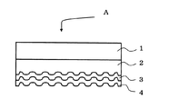
透明基材の一方の面に、ホログラム画像に対応した回折格子群を含むホログラムレリーフを有する透明樹脂層、前記ホログラムレリーフに接するように設けられた蛍光層、及び全反射性薄膜層が、この順序で設けられていることを特徴とするものである。
上記第1の態様のホログラムシートによれば、
透明基材の一方の面に、ホログラム画像に対応した回折格子群を含むホログラムレリーフを有する透明樹脂層、前記ホログラムレリーフに接するように設けられた蛍光層、及び全反射性薄膜層が、この順序で設けられていることを特徴とするホログラムシートを提供することができ、高い意匠性と高度な偽造防止性を持つホログラムシートを提供できる。
本発明のホログラムシートの第2の態様は、
前記蛍光層が、前記ホログラムレリーフを形成する凹凸に追従して均一な厚さで形成されていることを特徴とするものである。
上記第2の態様のホログラムシートによれば、
前記蛍光層が、前記ホログラムレリーフを形成する凹凸に追従して均一な厚さで形成されていることを特徴とする第1の態様のホログラムシートを提供することができ、より鮮明なホログラム再生像を出現可能な、ホログラムシートを提供できる。
本発明のホログラムシートの第3の態様は、
前記蛍光層の厚さが、0.01μm以上0.1μm以下であることを特徴とするものである。
To solve the above problem,
The first aspect of the hologram sheet of the present invention is:
A transparent resin layer having a hologram relief including a diffraction grating group corresponding to a hologram image, a fluorescent layer provided in contact with the hologram relief, and a total reflection thin film layer in this order on one surface of the transparent substrate. It is characterized by being provided with.
According to the hologram sheet of the first aspect,
A transparent resin layer having a hologram relief including a diffraction grating group corresponding to a hologram image, a fluorescent layer provided in contact with the hologram relief, and a total reflection thin film layer in this order on one surface of the transparent substrate. It is possible to provide a hologram sheet characterized in that the hologram sheet is provided with a high design property and a high level of forgery prevention.
The second aspect of the hologram sheet of the present invention is:
The fluorescent layer is formed with a uniform thickness following the unevenness forming the hologram relief.
According to the hologram sheet of the second aspect,
It is possible to provide the hologram sheet according to the first aspect, wherein the fluorescent layer is formed with a uniform thickness following the unevenness forming the hologram relief. Can be provided.
The third aspect of the hologram sheet of the present invention is:
The fluorescent layer has a thickness of 0.01 μm or more and 0.1 μm or less.
上記第3の態様のホログラムシートによれば、
前記蛍光層の厚さが、0.01μm以上0.1μm以下であることを特徴とする第2の態様のホログラムシートを提供することができ、鮮明度が著しく高いホログラム再生像を出現可能な、ホログラムシートを提供できる。
本発明のホログラムシートの第4の態様は、
前記透明樹脂層のホログラムレリーフが、
前記透明基材上に、均一な厚さの透明な層を形成し、前記透明な層上に、均一な厚さの蛍光層を形成した後に、前記透明な層と前記蛍光層とを同時に変形させることにより設けられたものであることを特徴とするものである。
上記第4の態様のホログラムシートによれば、
前記透明樹脂層のホログラムレリーフが、
前記透明基材上に、均一な厚さの透明な層を形成し、前記透明な層上に、均一な厚さの蛍光層を形成した後に、前記透明な層と前記蛍光層とを同時に変形させることにより設けられたものであることを特徴とする第2または第3のいずれかの態様のホログラムシートを提供することができ、自然光下でのホログラム再生像がより鮮明な、ホログラムシートを提供できる。
ホログラム画像を再生する回折格子群が、ホログラムレリーフとして、透明樹脂層面上に略一平面として形成されており、このホログラムレリーフ上に、且つ、このホログラムレリーフに追従して均一な厚さで蛍光層が設けられている。
すなわち、ホログラムレリーフは、位相ホログラムとしての位相差を「レリーフ形状」に現しているが、この位相差を有する「レリーフ形状」に追従して(沿って)蛍光層が設けられることにより、蛍光層が発する蛍光が、上記位相差を有して(含んで)発することになる。
According to the hologram sheet of the third aspect,
The hologram sheet according to the second aspect, wherein the fluorescent layer has a thickness of 0.01 μm or more and 0.1 μm or less, and can reproduce a hologram reproduction image with extremely high definition. A hologram sheet can be provided.
The fourth aspect of the hologram sheet of the present invention is:
The hologram relief of the transparent resin layer is
A transparent layer having a uniform thickness is formed on the transparent substrate, and a fluorescent layer having a uniform thickness is formed on the transparent layer, and then the transparent layer and the fluorescent layer are simultaneously deformed. It is characterized by being provided.
According to the hologram sheet of the fourth aspect,
The hologram relief of the transparent resin layer is
A transparent layer having a uniform thickness is formed on the transparent substrate, and a fluorescent layer having a uniform thickness is formed on the transparent layer, and then the transparent layer and the fluorescent layer are simultaneously deformed. It is possible to provide a hologram sheet according to any one of the second and third aspects characterized in that the hologram reproduction sheet is provided, and to provide a hologram sheet with a clearer hologram reproduction image under natural light. it can.
A diffraction grating group for reproducing a hologram image is formed as a hologram relief as a substantially flat surface on the surface of the transparent resin layer. On the hologram relief, the fluorescent layer has a uniform thickness following the hologram relief. Is provided.
In other words, the hologram relief shows the phase difference as a phase hologram in a “relief shape”, but the fluorescent layer is provided by following (along) the “relief shape” having this phase difference. Fluorescence emitted from the light will be emitted with (including) the phase difference.
そして、そのレリーフ形状をしている蛍光層のその「レリーフ形状」に追従して、さらにその蛍光層の上に、全反射性薄膜層が設けられている。
従って、全反射性薄膜層も、「レリーフ形状」を持ち、自然光下では、この蛍光層は視認されず、この全反射性薄膜層の反射面における「レリーフ形状」によって、ホログラム再生像を観察することとなる。
しかし、この蛍光層を発光させる照明光源、すなわち、定められた「所定の波長」を有する光源の照明を用いると、その「所定の波長」とは異なる「特定の波長のみ」によるホログラム再生像が特定の方向に出現して、観察者は、改めて、この「特定の波長」によるホログラム再生像を観察することとなる。
以下、この蛍光層によるホログラム再生の原理につき解説する。
すなわち、レリーフホログラムを再生する場合に生じるホイヘンスの2次波に対し、本発明のホログラムシートの場合において、この2次波に相当するものが、ホログラムレリーフ面に配された蛍光体(もしくは、蛍光物質とも呼ぶ。蛍光層の中に含まれている。)の蛍光発光であり、この発光がその役目を担い、ホログラム画像に対応した回折格子群を含むホログラムレリーフが有する位相差を含んで発光光を観察者側に発するものである。
この発光する光(以下、発光光ともいう。)が、ホログラムレリーフ面上の空間において干渉現象を起こし、その結果、所定の方向に所定のホログラム再生像を発現する。
蛍光体は、紫外線、電子線、X線などのエネルギーを吸収して可視光線として放出する物質であり、例えば、母体となるセラミックス結晶にEu やCe などの発光を担う金属イオンが微量添加した材料等がある。この場合、発光に寄与するのは金属イオンであり、外から加えられたエネルギー(紫外線、電子線、X線などや、もちろん可視光線、赤外線等のエネルギー。)を吸収して励起され、その後基底状態に戻る時に発光する。ホスト結晶の格子は金属イオンを取り囲むことによりイオンを化学的に安定化させたり、結晶場や配位環境を整えることにより発光色や発光強度を制御する働きをする。
本発明は、これらの蛍光発光の内、ストークスシフト(Stokes shift)によって可視光領域の発光を起こす蛍光体材料を用いる。もちろん、赤外線の励起による可視光領域の発光を起こすものも用いることができる。
Then, following the “relief shape” of the fluorescent layer having the relief shape, a total reflection thin film layer is further provided on the fluorescent layer.
Therefore, the total reflection thin film layer also has a “relief shape”, and this fluorescent layer is not visually recognized under natural light, and the hologram reproduction image is observed by the “relief shape” on the reflection surface of the total reflection thin film layer. It will be.
However, when an illumination light source that emits light from the fluorescent layer, that is, illumination of a light source having a predetermined “predetermined wavelength” is used, a hologram reproduction image by “only a specific wavelength” that is different from the “predetermined wavelength” is obtained. Appearing in a specific direction, the observer again observes the hologram reproduction image with this “specific wavelength”.
The principle of hologram reproduction by this fluorescent layer will be described below.
That is, in contrast to the Huygens secondary wave generated when the relief hologram is reproduced, in the case of the hologram sheet of the present invention, the secondary wave corresponds to the phosphor (or fluorescent light) arranged on the hologram relief surface. This light emission plays a role and includes the phase difference of the hologram relief including the diffraction grating group corresponding to the hologram image. Is emitted to the observer side.
This emitted light (hereinafter also referred to as emitted light) causes an interference phenomenon in the space on the hologram relief surface, and as a result, a predetermined hologram reproduction image is developed in a predetermined direction.
A phosphor is a substance that absorbs energy such as ultraviolet rays, electron beams, and X-rays and emits it as visible light. For example, a material obtained by adding a trace amount of metal ions responsible for light emission such as Eu and Ce to a base ceramic crystal. Etc. In this case, metal ions contribute to light emission and are excited by absorbing energy applied from outside (energy such as ultraviolet rays, electron beams, X-rays, and of course visible rays, infrared rays, etc.), and then the base. Lights when returning to the state. The lattice of the host crystal functions to chemically stabilize the ions by surrounding the metal ions, and to control the emission color and intensity by adjusting the crystal field and coordination environment.
The present invention uses a phosphor material that emits light in the visible light region by Stokes shift among these fluorescent emissions. Of course, a material that emits light in the visible light region due to infrared excitation can also be used.
本発明は、ホログラムの照明光源の波長とは異なる波長でホログラムを再生するものであり、例えば、紫外線で照明し、緑色のホログラムを視認することもできるため、観察者の目には、暗闇の中で、通常用いられる緑色の照明光源(例えば、アルゴンレーザーなど。)の無いところに、ホログラムだけが光輝き、空中に浮いているように見え、意匠性にも優れるものとなる。
また、単波長光源再生型であって、蛍光灯等の多波長光源による照明光下では、各波長によるホログラム再生像がダブってしまい(再生角度が僅かずつズレて再生し、「一つの鮮明な像」として観察できないことを意味する。)、ホログラム再生像を視認できないタイプのホログラムをレリーフホログラムとして記録しておくと、蛍光層から発する光が「単波長」であることから、「蛍光層が発光した時のみ観察可能となるようなホログラム」を含めることもでき、その意匠性及び偽造防止性を高めることを可能とする。
そして、通常のホログラムにおいては、その再生原理から、そのホログラム再生像が出現する方向がそのホログラムを照明する方向に依存しており、ホログラム再生用の照明を真上から斜め上方へと移動させると、ホログラム再生像の出現方向がその動きに同調して移動するものであるが、本発明のホログラムシートにおいては、全反射性薄膜層において反射されて再生するホログラム再生像は、これと同様の挙動を示すものの、蛍光層の発光により再生されるホログラム再生像は、その定められた「所定の波長」を有する光源の照明を、どのような方向からあてても、「同一の特定の方向にのみ現れる」という特異な性質を持つことから、その偽造防止性をさらに高めることができる。
もちろん、ホログラムを再生可能な光源の波長域が非常に狭いことに起因して、その特定の波長域を知りうる者のみがホログラム再生を果たすことができ、真正性判定用に有用なものとなる。また、上記したストークスシフトの値を知りうる者のみがホログラム再生像の色調を予測でき、その再生波長に調整したバンドパスフィルターを通して覗いて、そのバンドパスフィルターを通過できるホログラムのみが、真正であると判定することもできる。
また、このバンドパスフィルターを通過する角度(回折角度)も、そのストークスシフト量に依存し、やはり、その値を知りうる者のみがその特定の角度で判定を行うことができる。
さらに、蛍光体を複数含めることにより、この再生像は複数の角度に異なる色調で現れることになり、意匠性の面でも、真正性判定の面でもより優れたものとなる。
蛍光発光の原理は、図1に示すジャブロンスキー図にあるように、蛍光体(蛍光色素、蛍光顔料、蛍光染料等を含む。)の基底状態(S0:一重項状態)から光吸収によって第一(S1)、第二(S2)、第三励起状態(S3)・・・のどれかの振動状態に励起された発光体が、無放射過程で非常に速やかに緩和してS1の電子励起状態に移るか、あるいは項間交差によって三重項状態(T1、T2)へ移る。S1の最低振動状態になった蛍光体は、無放射過程によるか蛍光を発して基底状態に戻る。三重項状態になった分子は、無放射過程によるか、リン光を発して基底状態に戻る。
The present invention reproduces a hologram with a wavelength different from the wavelength of the illumination light source of the hologram. For example, it can be illuminated with ultraviolet rays and a green hologram can be visually recognized. Among them, only the hologram shines in a place without a normally used green illumination light source (for example, an argon laser), appears to float in the air, and is excellent in design.
In addition, in a single-wavelength light source reproduction type, under the illumination light from a multi-wavelength light source such as a fluorescent lamp, a hologram reproduction image at each wavelength is doubled (reproduction angle is slightly shifted and reproduced. Image) ”), and when a hologram of a type in which the hologram reproduction image cannot be visually recognized is recorded as a relief hologram, the light emitted from the fluorescent layer is“ single wavelength ”. It is also possible to include a “hologram that can be observed only when it emits light”, and it is possible to enhance its design and anti-counterfeiting properties.
In a normal hologram, due to its reproduction principle, the direction in which the hologram reproduction image appears depends on the direction of illuminating the hologram, and when the illumination for hologram reproduction is moved obliquely upward from directly above In the hologram sheet of the present invention, the hologram reproduction image that is reflected and reproduced by the total reflection thin film layer behaves in the same manner. However, the hologram reproduction image reproduced by the light emission of the fluorescent layer shows that the illumination of the light source having the predetermined “predetermined wavelength” is applied only in the same specific direction. Since it has a unique property of “appearing”, its anti-counterfeiting property can be further enhanced.
Of course, because the wavelength range of the light source capable of reproducing the hologram is very narrow, only those who know the specific wavelength range can reproduce the hologram, which is useful for authenticity determination. . Also, only those who can know the value of the Stokes shift described above can predict the color tone of the hologram reproduction image, and only the hologram that can pass through the bandpass filter by looking through the bandpass filter adjusted to the reproduction wavelength is authentic. It can also be determined.
Further, the angle (diffraction angle) passing through the bandpass filter also depends on the amount of Stokes shift, and only those who can know the value can make a determination at the specific angle.
Furthermore, by including a plurality of phosphors, this reproduced image appears in different colors at a plurality of angles, which is superior both in terms of design and authenticity.
As shown in the Jablonsky diagram shown in FIG. 1, the principle of fluorescence emission is first determined by light absorption from the ground state (S0: singlet state) of the phosphor (including fluorescent dye, fluorescent pigment, fluorescent dye, etc.). The luminescent material excited in any one of the vibration states (S1), second (S2), third excited state (S3),... Or the triplet state (T1, T2) by intersystem crossing. The phosphor in the lowest vibration state of S1 returns to the ground state due to a non-radiation process or emits fluorescence. The molecule in the triplet state returns to the ground state by a non-radiative process or phosphorescence.
一重項同士の遷移は瞬間的に起こるため、蛍光の半減期は10-4sec以下と短いものである。遷移に要する時間は、10-15secで励起が起こり、その後10-9〜10-7secで蛍光発光が起こるとされている。
一方、三重項から一重項への遷移はスピン変化禁止により禁制遷移となり自発的放出が起こりにくいので、リン光の半減期は大きく、秒単位のものもある。
基底状態に戻る際に光を発するか否か、光の強度が強いか弱いか、蛍光寿命が長いか短いかは、その蛍光体物質の分子構造や分子の置かれた環境に大きく依存する。
蛍光体材料の放出光の波長分布を蛍光スペクトルといい、蛍光スペクトルは蛍光の波長に対し相対的な蛍光強度をプロットして作成される。(実際の蛍光スペクトル測定では、波長と 強度が一定に維持された励起光を光源として用い、 蛍光体を取り扱う場合は、放出スペクトルのことを蛍光スペクトルと呼ぶ。)蛍光スペクトルに示される波長(エネルギー)は一次励起状態の最低振動エネルギー準位から基底状態の優先的な振動エネルギー準位までのエネルギー差と等しくなる。
蛍光の振幅が励起状態と基底状態の振幅構造と類似しているなら、最も長波長側の励起の振幅と鏡像関係となり、理論上、蛍光色素が吸収した光エネルギーの波長と蛍光として放出する波長は同じになる。しかし実際にはほとんどの蛍光色素の蛍光スペクトルは長波長(低エネルギー)側にシフトする。励起スペクトルと蛍光スペクトルのピーク波長間の差はストークスシフトと呼ばれ、この波長差は、蛍光放出以前の励起状態の際に放出されたエネルギーが熱エネルギーに変換されたために生じる。
ストークスシフトは蛍光の感度おいて非常に重要であり、蛍光を検出する際、励起光の影響を受けないためバックグラウンドを低くすることができる。
入射光の波長と強度を一定にした場合(例えば、光源として制御されたレーザー光を使用した場合)、放出される蛍光は蛍光物質の量と正比例する。従って、蛍光の強度を一定とするためには、ホログラムレリーフ面に形成する蛍光層の中の蛍光体の量を一定とする必要がある。
Since the transition between singlets occurs instantaneously, the half-life of fluorescence is as short as 10 −4 sec or less. The time required for the transition is said to be excited at 10 −15 sec and then to emit fluorescence at 10 −9 to 10 −7 sec.
On the other hand, the transition from triplet to singlet is forbidden due to the prohibition of spin change, and spontaneous emission is difficult to occur.
Whether or not light is emitted when returning to the ground state, whether the intensity of light is strong or weak, and whether the fluorescence lifetime is long or short largely depends on the molecular structure of the phosphor material and the environment in which the molecule is placed.
The wavelength distribution of the emitted light of the phosphor material is called a fluorescence spectrum, and the fluorescence spectrum is created by plotting the fluorescence intensity relative to the fluorescence wavelength. (In actual fluorescence spectrum measurement, excitation light with a constant wavelength and intensity is used as the light source, and when dealing with phosphors, the emission spectrum is called the fluorescence spectrum.) The wavelength (energy) shown in the fluorescence spectrum ) Is equal to the energy difference from the lowest vibration energy level in the primary excited state to the preferential vibration energy level in the ground state.
If the amplitude of the fluorescence is similar to the amplitude structure of the excited state and the ground state, the wavelength of the light energy absorbed by the fluorescent dye and the wavelength emitted as fluorescence are theoretically related to the amplitude of the excitation on the longest wavelength side. Will be the same. However, in practice, the fluorescence spectrum of most fluorescent dyes shifts to the longer wavelength (low energy) side. The difference between the peak wavelengths of the excitation spectrum and the fluorescence spectrum is called the Stokes shift, and this wavelength difference is caused by the energy released in the excited state before the emission of fluorescence being converted into thermal energy.
The Stokes shift is very important in the sensitivity of fluorescence, and when detecting fluorescence, the background can be lowered because it is not affected by excitation light.
When the wavelength and intensity of incident light are constant (for example, when controlled laser light is used as a light source), the emitted fluorescence is directly proportional to the amount of fluorescent material. Therefore, in order to make the fluorescence intensity constant, it is necessary to make the amount of the phosphor in the fluorescent layer formed on the hologram relief surface constant.
もちろん、蛍光体の濃度が高い場合には、サチレーションをおこし直線性が失われて一定の強度となったり、蛍光体間の距離が極めて接近し、表面付近だけが励起され、放出蛍光が吸収されてしまうため、本発明の目的である蛍光光の干渉性を十分得るためには、蛍光層の厚さ方向に蛍光体が分散して多く存在するよりも、ホログラムレリーフ面近傍にのみ均一に存在する方が、より高い干渉現象を生じるため、蛍光体の粒径の1〜10倍、さらには1〜3倍とすることが望ましい。蛍光体が染料であり、蛍光層を形成する樹脂に溶解している場合には、その樹脂層を薄く抑える必要がある。また、蛍光染料によって、染着する場合には、ホログラムレリーフを形成している透明樹脂層そのもののレリーフ面のみを染着することにより、上記した目的を達成することもできる。
また、蛍光体によっては、放出される蛍光強度(輝度)が異なり、蛍光強度はそのまま感度に影響を与えるため蛍光体の蛍光強度は非常に重要な要素となる。蛍光強度は蛍光体の以下の2つの特性に依存し、
・光の吸収効率(吸光係数)
・励起光と蛍光の変換効率(量子収率)
蛍光強度は蛍光体の吸光係数(ε)と量子収率(φ)に比例するため、以下の式で表される。
・蛍光強度(輝度) ∝ 吸光係数(ε)×量子収率(φ)
ここで、蛍光体の吸光係数とは蛍光体に吸収される特定波長の光量を意味し、モル吸光係数は光路1 cmあたりの1M(1モル)蛍光色素溶液の光学濃度として定義される。有用な蛍光体では、このモル吸光係数が10,000以上を示す。励起光と蛍光の変換効率(量子収率)は以下の式から得ることができる。
・φ = 放出された光子数 / 吸収された光子数
ここで、量子収率(φ)は “0” (非蛍光性物質)から “1” (効率100%)までの値をとる。蛍光体の量子収率を示す例として、フルオレセイン(φ=0.9)およびCy5(φ=0.3)がある。通常の量子収率(φ)の測定には、吸収スペクトルのピーク波長が用いられる。
Of course, when the concentration of the phosphor is high, saturation occurs and the linearity is lost, resulting in a constant intensity, or the distance between the phosphors is very close, and only the vicinity of the surface is excited and the emitted fluorescence is absorbed. Therefore, in order to sufficiently obtain the coherence of fluorescent light, which is the object of the present invention, it exists uniformly only in the vicinity of the hologram relief surface, rather than a large amount of phosphors dispersed in the thickness direction of the fluorescent layer. In order to produce a higher interference phenomenon, it is desirable that the particle size is 1 to 10 times, more preferably 1 to 3 times the particle size of the phosphor. When the phosphor is a dye and is dissolved in the resin forming the fluorescent layer, it is necessary to keep the resin layer thin. When dyeing with a fluorescent dye, the above-mentioned object can be achieved by dyeing only the relief surface of the transparent resin layer itself forming the hologram relief.
Also, depending on the phosphor, the emitted fluorescence intensity (brightness) varies, and the fluorescence intensity directly affects the sensitivity, so the fluorescence intensity of the phosphor is a very important factor. The fluorescence intensity depends on the following two characteristics of the phosphor:
・ Light absorption efficiency (absorption coefficient)
-Conversion efficiency between excitation light and fluorescence (quantum yield)
Since the fluorescence intensity is proportional to the extinction coefficient (ε) and quantum yield (φ) of the phosphor, it is expressed by the following equation.
・ Fluorescence intensity (luminance) 吸 光 Absorption coefficient (ε) × quantum yield (φ)
Here, the extinction coefficient of the phosphor means the amount of light of a specific wavelength absorbed by the phosphor, and the molar extinction coefficient is defined as the optical density of a 1M (1 mol) fluorescent dye solution per 1 cm of the optical path. Useful phosphors have a molar extinction coefficient of 10,000 or more. The conversion efficiency (quantum yield) between excitation light and fluorescence can be obtained from the following equation.
Φ = number of emitted photons / number of absorbed photons Here, the quantum yield (φ) ranges from “0” (non-fluorescent substance) to “1” (efficiency 100%). Examples showing the quantum yield of the phosphor include fluorescein (φ = 0.9) and Cy5 (φ = 0.3). The peak wavelength of the absorption spectrum is used for the usual quantum yield (φ) measurement.
フルオレセイン(ε=70,000、φ=0.9) とCy5(ε=200,000、φ=0.3)は極めて高い輝度を持っており、これらの蛍光体は量子収率と吸光係数は非常に異なっているが、蛍光強度は同等となる。
したがって、蛍光体を評価する場合は、吸光係数と量子収率をあわせて考慮する必要がある。蛍光強度は入射光の強さにも影響を受け、理論上、入射光量を上げていくと励起さ
れる蛍光体が増加し、同時に放出される光量(光子数、あるいは基底状態まで落ちていく 電子数)が増加し、蛍光強度の上昇として観察される。しかし 実際には、入射光量を上げすぎてしまうと全ての蛍光体が常時励起状態となり、蛍光破壊が起こり蛍光強度が減衰あるいは消失して蛍光強度との相関性が失われる等の現象が発生するため、入射光量を適切に定める必要がある。
さらに、蛍光体の量子収率や励起スペクトルおよび蛍光スペクトルは 環境条件、すなわち、環境温度、イオン濃度、PH、励起光の強度、樹脂等との共有結合、非共有結合性の相互作用(インターカレーション効果等。)などから影響を受けるため、これら環境条件を考慮して励起光波長や、蛍光光を認識しやすくするための光学フィルター(ロウパスフィルター、ハイパスフィルターや、バンドパスフィルター等。)を必要に応じ、設定する必要がある場合もある。
Fluorescein (ε = 70,000, φ = 0.9) and Cy5 (ε = 200,000, φ = 0.3) have extremely high luminance, and these phosphors have quantum yields and extinction coefficients. Although very different, the fluorescence intensity is equivalent.
Therefore, when evaluating the phosphor, it is necessary to consider both the extinction coefficient and the quantum yield. Fluorescence intensity is also affected by the intensity of incident light. Theoretically, when the amount of incident light is increased, the number of excited phosphors increases, and the amount of emitted light (the number of photons or the ground state falls to the ground state) Number) increases and is observed as an increase in fluorescence intensity. However, in reality, if the incident light intensity is increased too much, all the phosphors are always excited, causing fluorescence destruction, resulting in attenuation or disappearance of the fluorescence intensity and loss of correlation with the fluorescence intensity. Therefore, it is necessary to appropriately determine the amount of incident light.
In addition, the quantum yield, excitation spectrum, and fluorescence spectrum of the phosphor are determined based on environmental conditions, that is, environmental temperature, ion concentration, pH, excitation light intensity, covalent bond with resin, non-covalent interaction (intercalation The optical filter (low-pass filter, high-pass filter, band-pass filter, etc.) that makes it easy to recognize the excitation light wavelength and fluorescent light in consideration of these environmental conditions. May need to be set as needed.
また、もう1つの環境効果として光によるフォトブリーチングがある。励起状態にある蛍光体は基底状態に比べて化学的に活性化されているため、破壊されやすくなり、低頻度ではあるが、例えば、「励起蛍光色素分子」が化学反応を進行し、最終的に低蛍光性の構造になりことがある。この化学反応の進行は個々の蛍光体のフォトブリーチングに対する感受性や化学的な環境、励起光の強度、励起光の照射時間、観察や認証のための光学スキャンの繰り返し数等に依存するため、目的に応じた設定が必要となる。
光源として制御可能なレーザー光を使用するなど、入射光の波長と強度を一定にした場合、放出される蛍光(光子数)は蛍光体の量と正比例する。蛍光体が極めて高濃度である場合は、シグナル応答が非線形になる。
一定量の蛍光体から放出される光子数は、励起/放出サイク ルを繰り返せば増幅できる。励起光強度と蛍光体濃度が一定の場合は、放出光の総量は照射時間(蛍光色素等に励起光を照射している期間)に比例する。励起/放出サイクルの時間よりも照射時間が長ければ、蛍光体は励起/放出サイクルを何回も繰り返す。蛍光強度(放出光子数)の測定は、どのような受光素子でも測定可能である。
低強度光を測定する場合は、 増幅機構を持つ光電子増幅管(Photo multiplier tube:PMT) が有効である。PMTに十分なエネルギーを持つ光が入射すると、 陰極から電子が放出され、電子は電流として増幅される。これら受光素子の電流は、入射光の強度に比例し、蛍光強度は通常、任意単位で表示される(例rfu:rela−tive fluorescence unites:相対蛍光単位)。
Another environmental effect is photobleaching with light. Since the phosphor in the excited state is chemically activated as compared with the ground state, it is more likely to be destroyed and, for example, the “excited fluorescent dye molecule” proceeds with a chemical reaction, but is less frequent. May have a low fluorescence structure. The progress of this chemical reaction depends on the sensitivity of individual phosphors to photobleaching and the chemical environment, the intensity of excitation light, the irradiation time of excitation light, the number of repetitions of optical scans for observation and authentication, etc. Settings according to the purpose are required.
When the wavelength and intensity of incident light are made constant, such as when a controllable laser beam is used as the light source, the emitted fluorescence (number of photons) is directly proportional to the amount of phosphor. If the phosphor is at a very high concentration, the signal response is non-linear.
The number of photons emitted from a certain amount of phosphor can be amplified by repeating the excitation / emission cycle. When the excitation light intensity and the phosphor concentration are constant, the total amount of emitted light is proportional to the irradiation time (period in which excitation light is irradiated to a fluorescent dye or the like). If the irradiation time is longer than the time of the excitation / emission cycle, the phosphor repeats the excitation / emission cycle many times. The fluorescence intensity (number of emitted photons) can be measured by any light receiving element.
When measuring low-intensity light, a photomultiplier tube (PMT) having an amplification mechanism is effective. When light having sufficient energy enters the PMT, electrons are emitted from the cathode, and the electrons are amplified as a current. The currents of these light receiving elements are proportional to the intensity of incident light, and the fluorescence intensity is usually displayed in arbitrary units (eg, rfu: relative-fluorescence units).
蛍光体は、一般的に、蛍光体原料を焼成する固相反応法により、製造される。この固相反応法では原料混合物を高い温度で焼成するため、得られる焼成ケーキは、蛍光体粒子が硬く凝集したものとなることが多い。そのため、通常は、蛍光体の製造の際には例えばボールミル、乳鉢等による粉砕工程を行うが、このときの蛍光体粒子の表面の損傷を抑制する方法として、流動式反応器装置を用いて、実質的に単分散の蛍光体−前駆体粒子を、流動する気体中に浮遊させて焼成することにより、凝集していない実質的に単分散の蛍光性粒子を製造する。この方法によれば、1μm未満の大きさの蛍光性粒子を製造することができる。
また、例えば、ZnGa2O4:Mn蛍光体を製造するに際し、焼成を行なう前の蛍光体原料を湿式沈殿法により調製することにより、低温での焼成が可能となり、蛍光体粒子の凝集を抑制することができる。
また、例えば、アルカリ土類アルミン酸塩系、またはアルカリ土類珪酸塩系の母体結晶を有する蛍光体の製造方法に関し、Srを含む蛍光体原料として硝酸ストロンチウムを用い、原料混合液又は懸濁液を所望の粒径となるよう液滴化し、これを焼成する方法がある。これにより、極めて脆い性質を有する蛍光体が得られ、容易に微小なサイズへ粉砕することができる。
蛍光体原料としては、製造しようとする蛍光体を構成する元素(以下、「蛍光体構
成元素」ともいう。)を含有する化合物を用いることができる。その例を挙げると、蛍光体構成元素を含有する、酸化物、水酸化物、炭酸塩、硝酸塩、硫酸塩、蓚酸塩、カルボン酸塩、ハロゲン化物、窒化物等が挙げられる。蛍光体原料の選択に際しては、得られる蛍光体への反応性等を考慮して選択することが好ましい。さらに、蛍光体を構成する各蛍光体構成元素に対応し、蛍光体原料は、それぞれ、1種を用いてもよく、2種以上を任意の組み合わせ及び比率で併用しても良い。
また、蛍光体の各蛍光体原料中に含まれる不純物としては、蛍光体の特性に悪影響を与えない限りにおいて、特に限定されない。
各蛍光体原料の重量メジアン径としては、通常0.01μm以上、0.5μm以下である。このために、蛍光体原料の種類によっては予めジェットミル等の乾式粉砕機で粉砕を行っても良い。これにより、各蛍光体原料の原料混合物中での均一分散化を図り、かつ、蛍光体原料の表面積増大による原料混合物の固相反応性を高めることができ、不純物相の生成を抑えることが可能となる。
The phosphor is generally manufactured by a solid phase reaction method in which a phosphor material is fired. In this solid phase reaction method, since the raw material mixture is fired at a high temperature, the obtained fired cake is often a product in which phosphor particles are hard and aggregated. Therefore, normally, when producing the phosphor, for example, a pulverization step using a ball mill, a mortar, etc., is performed, but as a method for suppressing damage to the surface of the phosphor particles at this time, using a fluid reactor device, Substantially monodispersed phosphor-precursor particles are suspended in a flowing gas and baked to produce substantially monodispersed fluorescent particles that are not aggregated. According to this method, fluorescent particles having a size of less than 1 μm can be produced.
In addition, for example, when manufacturing a ZnGa 2 O 4 : Mn phosphor, the phosphor raw material before firing is prepared by a wet precipitation method, which enables firing at a low temperature and suppresses aggregation of phosphor particles. can do.
Further, for example, regarding a method for producing a phosphor having an alkaline earth aluminate-based or alkaline earth silicate-based host crystal, strontium nitrate is used as a phosphor raw material containing Sr, and a raw material mixture or suspension There is a method of forming droplets so as to have a desired particle diameter and firing the droplets. As a result, a phosphor having extremely brittle properties can be obtained and can be easily pulverized to a minute size.
As the phosphor material, a compound containing an element constituting the phosphor to be manufactured (hereinafter also referred to as “phosphor constituent element”) can be used. Examples thereof include oxides, hydroxides, carbonates, nitrates, sulfates, oxalates, carboxylates, halides, nitrides and the like containing phosphor constituent elements. When selecting the phosphor raw material, it is preferable to select in consideration of the reactivity to the obtained phosphor. Furthermore, corresponding to each phosphor constituting element constituting the phosphor, one kind of phosphor raw material may be used, or two or more kinds may be used in combination in any combination and ratio.
Further, the impurities contained in each phosphor raw material of the phosphor are not particularly limited as long as the phosphor characteristics are not adversely affected.
The weight median diameter of each phosphor material is usually 0.01 μm or more and 0.5 μm or less. For this reason, depending on the type of the phosphor material, pulverization may be performed in advance by a dry pulverizer such as a jet mill. As a result, each phosphor raw material can be uniformly dispersed in the raw material mixture, and the solid phase reactivity of the raw material mixture can be increased by increasing the surface area of the phosphor raw material, thereby suppressing the generation of impurity phases. It becomes.
例えば、Baを含む蛍光体原料の具体例としては、BaO、Ba(OH)2・8H2O、BaCO3、Ba(NO3)2、BaSO4、Ba(C2O4)・2H2O、Ba(OCOCH3)2、BaCl2等が挙げられる。
Caを含む蛍光体原料の具体例としては、CaO、Ca(OH)2、CaCO3、Ca(NO3)2・4H2O、CaSO4・2H2O、Ca(C2O4)・H2O、Ca(OCOCH3)2・H2O、無水CaCl2(但し、水和物であってもよい。)等が挙げられる。
Srを含む蛍光体原料の具体例としては、SrO、Sr(OH)2・8H2O、SrCO3、Sr(NO3)2、SrSO4、Sr(C2O4)・H2O、Sr(OCOCH3)2・0.5H2O、SrCl2等が挙げられる。
Znを含む蛍光体原料の具体例としては、ZnO、Zn(C2O4)・2H2O、ZnSO4・7H2O等が挙げられる。
Mgを含む蛍光体原料の具体例としては、MgCO3、MgO、MgSO4、Mg(C2O4)・2H2O等が挙げられる。
Siを含む蛍光体原料の具体例としては、SiO2、H4SiO4、Si(OCOCH3)4等が挙げられる。
Euを含む蛍光体原料の具体例としては、Eu2O3、Eu2(SO4)3、Eu2(C2O4)3、EuCl2、EuCl3、Eu(NO3)3・6H2O等が挙げられる。
Sm、Tm及びYbを含む各蛍光体原料の具体例としては、Eu源の具体例として挙げた各化合物において、EuをそれぞれSm、Tm及びYbに置き換えた化合物が挙げられる。
For example, specific examples of phosphor materials containing Ba include BaO, Ba (OH) 2 .8H 2 O, BaCO 3 , Ba (NO 3 ) 2 , BaSO 4 , Ba (C 2 O 4 ) · 2 H 2. O, Ba (OCOCH 3 ) 2 , BaCl 2 and the like.
Specific examples of phosphor raw materials containing Ca include CaO, Ca (OH) 2 , CaCO 3 , Ca (NO 3 ) 2 .4H 2 O, CaSO 4 .2H 2 O, Ca (C 2 O 4 ) · H. 2 O, Ca (OCOCH 3 ) 2 .H 2 O, anhydrous CaCl 2 (however, it may be a hydrate).
Specific examples of the phosphor raw material containing Sr include SrO, Sr (OH) 2 .8H 2 O, SrCO 3 , Sr (NO 3 ) 2 , SrSO 4 , Sr (C 2 O 4 ) · H 2 O, Sr. (OCOCH 3 ) 2 · 0.5H 2 O, SrCl 2 and the like.
Specific examples of the phosphor material containing Zn include ZnO, Zn (C 2 O 4 ) · 2H 2 O, ZnSO 4 · 7H 2 O, and the like.
Specific examples of the phosphor raw material containing Mg include MgCO 3 , MgO, MgSO 4 , Mg (C 2 O 4 ) · 2H 2 O, and the like.
Specific examples of the phosphor raw material containing Si include SiO 2 , H 4 SiO 4 , Si (OCOCH 3 ) 4 and the like.
Specific examples of the phosphor material containing Eu include Eu 2 O 3 , Eu 2 (SO 4 ) 3 , Eu 2 (C 2 O 4 ) 3 , EuCl 2 , EuCl 3 , Eu (NO 3 ) 3 .6H 2. O etc. are mentioned.
Specific examples of each phosphor raw material containing Sm, Tm, and Yb include compounds in which Eu is replaced with Sm, Tm, and Yb, respectively, in the compounds listed as specific examples of the Eu source.
Mnを含む蛍光体原料の具体例としては、MnO、MnO2、Mn2O3、MnF2、MnCl2、MnBr2、Mn(NO3)2・6H2O、MnCO3、MnCr2O4等が挙げられる。
Crを含む蛍光体原料の具体例としては、Cr2O3、CrF3(水和物であってもよい)、CrCl3、CrBr3・6H2O、Cr(NO3)2・9H2O、(NH4)2CrO4等が挙げられる。
Tbを含む蛍光体原料の具体例としては、Tb4O7、TbCl3(水和物を含む。)、TbF3、Tb(NO3)3・nH2O、Tb2(SiO4)3、Tb2(C2O4)3・10H2O等が挙げられる。また、他の蛍光体原料(例えば、Eu源)とTb源とを共沈させてから用いることもできる。
Prを含む蛍光体原料の具体例としては、Pr2O3、PrCl3、PrF3、Pr(NO3)3・6H2O、Pr2(SiO4)3、Pr2(C2O4)3・10H2O等が挙げられる。
Ceを含む蛍光体原料の具体例としては、CeO2、CeCl3、Ce2(CO3)3・5H2O、CeF3、Ce(NO3)3・6H2O等が挙げられる。
Luを含む蛍光体原料の具体例としては、Lu2O3、LuCl3、LuF3(水和物であってもよい)、Lu(NO3)3(水和物であってもよい)等が挙げられる。
Laを含む蛍光体原料の具体例としては、La2O3、LaCl3・7H2O、La2(CO3)3・H2O、LaF3、La(NO3)3・6H2O、La2(SO4)3等が挙げられる。
Gdを含む蛍光体原料の具体例としては、Gd2O3、GdCl3・6H2O、Gd(NO3)3・5H2O、Gd2(SO4)3・8H2O、GdF3等が挙げられる。
Specific examples of the phosphor raw material containing Mn include MnO, MnO 2 , Mn 2 O 3 , MnF 2 , MnCl 2 , MnBr 2 , Mn (NO 3 ) 2 .6H 2 O, MnCO 3 , MnCr 2 O 4 and the like. Is mentioned.
Specific examples of the phosphor material containing Cr include Cr 2 O 3 , CrF 3 (may be a hydrate), CrCl 3 , CrBr 3 .6H 2 O, Cr (NO 3 ) 2 .9H 2 O. , (NH 4 ) 2 CrO 4 and the like.
Specific examples of the phosphor raw material containing Tb include Tb 4 O 7 , TbCl 3 (including hydrate), TbF 3 , Tb (NO 3 ) 3 .nH 2 O, Tb 2 (SiO 4 ) 3 , Examples thereof include Tb 2 (C 2 O 4 ) 3 · 10H 2 O. Further, other phosphor materials (for example, Eu source) and Tb source may be co-precipitated before use.
Examples of phosphor materials containing Pr, Pr 2 O 3, PrCl 3,
Specific examples of the phosphor raw material containing Ce include CeO 2 , CeCl 3 , Ce 2 (CO 3 ) 3 .5H 2 O, CeF 3 , Ce (NO 3 ) 3 .6H 2 O, and the like.
Specific examples of the phosphor material containing Lu include Lu 2 O 3 , LuCl 3 , LuF 3 (may be a hydrate), Lu (NO 3 ) 3 (may be a hydrate), etc. Is mentioned.
Specific examples of phosphor raw materials containing La include La 2 O 3 , LaCl 3 · 7 H 2 O, La 2 (CO 3 ) 3 · H 2 O, LaF 3 , La (NO 3 ) 3 · 6H 2 O. , La 2 (SO 4 ) 3 and the like.
Specific examples of the phosphor material containing Gd include Gd 2 O 3 , GdCl 3 .6H 2 O, Gd (NO 3 ) 3 .5H 2 O, Gd 2 (SO 4 ) 3 / 8H 2 O, GdF 3 and the like. Is mentioned.
Geを含む蛍光体原料の具体例としては、GeO2、Ge(OH)4、Ge(OCOCH3)4、GeCl4等が挙げられる。
Gaを含む蛍光体原料の具体例としては、Ga2O3、Ga(OH)3、Ga(NO3)3・nH2O、Ga2(SO4)3、GaCl3等が挙げられる。
Alを含む蛍光体原料の具体例としてはα−Al2O3、γ−Al2O3等のAl2O3、Al(OH)3、AlOOH、Al(NO3)3・9H2O、Al2(SO4)3、AlCl3等が挙げられる。
Pを含む蛍光体原料の具体例としては、P2O5、Ba3(PO4)2、Sr3(PO4)2、(NH4)3PO4等が挙げられる。
Bを含む蛍光体原料の具体例としては、B2O3、H3BO3等が挙げられる。
なお、上記に例示した原料は、必要に応じて共沈させてから用いてもよい。
さらに、N元素、O元素及びハロゲン元素等に対応する蛍光体原料は、通常、上記各蛍光体構成元素の蛍光体原料のアニオン成分として、又は焼成雰囲気中に含有される成分として、蛍光体製造時に供給される。
蛍光体原料を混合して原料混合物を調製してから、原料混合物を所定温度、雰囲気下で焼成する。この際、混合は十分に行うことが好ましい。
上記混合手法としては、特に限定はされないが、具体的には、下記(A)及び(B)として挙げた手法を用いることができる。また、これらの各種条件については、例えば、ボールミルにおいて2種の粒径の異なるボールを混合して用いる等の条件を選択可能である
。
Specific examples of the phosphor material containing Ge include GeO 2 , Ge (OH) 4 , Ge (OCOCH 3 ) 4 , GeCl 4 and the like.
Specific examples of the phosphor material containing Ga include Ga 2 O 3 , Ga (OH) 3 , Ga (NO 3 ) 3 .nH 2 O, Ga 2 (SO 4 ) 3 , and GaCl 3 .
Specific examples of the phosphor material containing Al include Al 2 O 3 such as α-Al 2 O 3 and γ-Al 2 O 3 , Al (OH) 3 , AlOOH, Al (NO 3 ) 3 · 9H 2 O, Examples include Al 2 (SO 4 ) 3 and AlCl 3 .
Specific examples of the phosphor raw material containing P include P 2 O 5 , Ba 3 (PO 4 ) 2 , Sr 3 (PO 4 ) 2 , (NH 4 ) 3 PO 4 and the like.
Specific examples of the phosphor raw material containing B include B 2 O 3 and H 3 BO 3 .
In addition, you may use the raw material illustrated above, after coprecipitating as needed.
Further, phosphor raw materials corresponding to N element, O element, halogen element, etc. are usually manufactured as phosphors as anion components of the phosphor raw materials of the respective phosphor constituting elements or as components contained in the firing atmosphere. Sometimes supplied.
After preparing a raw material mixture by mixing phosphor raw materials, the raw material mixture is fired at a predetermined temperature and atmosphere. At this time, it is preferable to perform the mixing sufficiently.
Although it does not specifically limit as said mixing method, Specifically, the method quoted as the following (A) and (B) can be used. As for these various conditions, for example, it is possible to select conditions such as mixing and using two kinds of balls having different particle diameters in a ball mill.
(A)例えばハンマーミル、ロールミル、ボールミル、ジェットミル等の乾式粉砕機、又は、乳鉢と乳棒等を用いる粉砕と、例えばリボンブレンダー、V型ブレンダー、ヘンシェルミキサー等の混合機、又は、乳鉢と乳棒を用いる混合とを組み合わせ、前述の蛍光体原料を粉砕混合する乾式混合法。
(B)前述の蛍光体原料に例えばメタノール、エタノール等のアルコール系溶媒又は水などの溶媒又は分散媒を加え、例えば粉砕機、乳鉢と乳棒、又は蒸発皿と撹拌棒等を用いて混合し、溶液又はスラリーの状態とした上で、噴霧乾燥、加熱乾燥、又は自然乾燥等により乾燥させる湿式混合法。
蛍光体原料の混合は、蛍光体原料の物性に応じて、湿式又は乾式のいずれかを選択することができる。
また、ハロゲン化物、窒化物等の酸化・吸湿し易い原料を用いる場合には、例えばアルゴンガス、窒素ガス等の不活性気体を充填し、水分管理されたグローブボックス内でミキサー混合する。
また、混合・粉砕時に、粒径を揃える等の目的で、蛍光体原料を篩いにかけても良い。この場合、各種市販の篩いを用いることが可能であるが、金属メッシュのものよりもナイロンメッシュ等の樹脂製のものを用いる方が、不純物混入防止の点で好ましい。
焼成工程では、得られた原料混合物を焼成することにより焼成物を得る。得られた焼成物は、通常、その組成は目的とする蛍光体のものとなっているが、その粒子は焼結して焼成ケーキとなっている。
(A) Dry pulverizer such as hammer mill, roll mill, ball mill, jet mill, etc., or pulverization using mortar and pestle, and mixer such as ribbon blender, V-type blender, Henschel mixer, or mortar and pestle And a dry mixing method in which the above phosphor raw materials are pulverized and mixed.
(B) Add a solvent or dispersion medium such as an alcohol solvent such as methanol or ethanol or water to the phosphor raw material, and mix using, for example, a pulverizer, a mortar and pestle, or an evaporating dish and a stirring bar, A wet mixing method in which a solution or slurry is made and then dried by spray drying, heat drying, or natural drying.
The mixing of the phosphor raw material can be either wet or dry depending on the physical properties of the phosphor raw material.
In addition, when using a material that easily oxidizes and absorbs moisture, such as halide and nitride, for example, an inert gas such as argon gas or nitrogen gas is filled and mixed in a glove box in which moisture is controlled.
In addition, the phosphor material may be sieved for the purpose of, for example, uniforming the particle size during mixing and pulverization. In this case, various types of commercially available sieves can be used, but it is preferable to use a resin mesh such as a nylon mesh rather than a metal mesh in terms of preventing impurities from being mixed.
In the firing step, a fired product is obtained by firing the obtained raw material mixture. The obtained fired product usually has the composition of the intended phosphor, but the particles are sintered into a fired cake.
さらに、焼成において、焼成炉中の耐熱容器の数が多い場合には、例えば、上記の昇温速度を遅めにする等、各耐熱容器への熱の伝わり具合を均等にすることが、ムラなく焼成するためには好ましい。
焼成工程における焼成温度、圧力、雰囲気等の焼成条件は、製造しようとする蛍光体そ
れぞれに応じて適切な条件を設定することが好ましい。
さらに、耐湿性等の耐候性を一層向上させるために、又は、発光装置の蛍光体含有部における樹脂に対する分散性を向上させるために、必要に応じて、蛍光体の表面を異なる物質で被覆する等の表面処理を行なってもよい。
蛍光体の表面に存在させることのできる物質(以下「表面処理物質」とも称する。)の例としては、例えば、有機化合物、無機化合物、ガラス材料等を挙げることができる。 有機化合物の例としては、アクリル樹脂、ポリカーボネート、ポリアミド、ポリエチレン等の熱溶融性ポリマー、ラテックス、ポリオルガノシロキサン等が挙げられる。
無機化合物の例としては、酸化マグネシウム、酸化アルミニウム、酸化珪素、酸化チタン、酸化ジルコニウム、酸化スズ、酸化ゲルマニウム、酸化タンタル、酸化ニオブ、酸化バナジウム、酸化硼素、酸化アンチモン、酸化亜鉛、酸化イットリウム、酸化ランタン、酸化ビスマス等の金属酸化物、窒化珪素、窒化アルミニウム等の金属窒化物、燐酸カルシウム、燐酸バリウム、燐酸ストロンチウム等のオルト燐酸塩、ポリリン酸塩等が挙げられる。なお、燐酸リチウム、燐酸ナトリウム、及び燐酸カリウムからなる群から選ばれる少なくとも1種と、硝酸バリウム、硝酸カルシウム、硝酸ストロンチウム、塩酸バリウム、塩酸カルシウム、及び塩酸ストロンチウムからなる群から選ばれる少なくとも1種とを組み合わせて用いることもできる。中でも、燐酸ナトリウムと硝酸カルシウムとを組み合わせて用いることが好ましい。また、蛍光体表面にバリウム、カルシウム、ストロンチウムが存在する場合には燐酸ナトリウム等の燐酸塩のみを用いても表面処理を行なうことができる。
Furthermore, when the number of heat-resistant containers in the baking furnace is large in baking, for example, the rate of heat transfer to each heat-resistant container can be made uniform, for example, by slowing the temperature increase rate. It is preferable for firing without any problems.
The firing conditions such as the firing temperature, pressure, and atmosphere in the firing step are preferably set appropriately for each phosphor to be manufactured.
Furthermore, in order to further improve the weather resistance such as moisture resistance or to improve the dispersibility of the phosphor in the phosphor-containing part of the light emitting device, the surface of the phosphor is coated with a different substance as necessary. You may perform surface treatments, such as.
Examples of substances that can be present on the surface of the phosphor (hereinafter also referred to as “surface treatment substances”) include organic compounds, inorganic compounds, glass materials, and the like. Examples of the organic compound include acrylic resins, heat-meltable polymers such as polycarbonate, polyamide, and polyethylene, latex, polyorganosiloxane, and the like.
Examples of inorganic compounds include magnesium oxide, aluminum oxide, silicon oxide, titanium oxide, zirconium oxide, tin oxide, germanium oxide, tantalum oxide, niobium oxide, vanadium oxide, boron oxide, antimony oxide, zinc oxide, yttrium oxide, oxide Examples thereof include metal oxides such as lanthanum and bismuth oxide, metal nitrides such as silicon nitride and aluminum nitride, orthophosphates such as calcium phosphate, barium phosphate, and strontium phosphate, and polyphosphates. And at least one selected from the group consisting of lithium phosphate, sodium phosphate, and potassium phosphate, and at least one selected from the group consisting of barium nitrate, calcium nitrate, strontium nitrate, barium hydrochloride, calcium hydrochloride, and strontium hydrochloride. Can also be used in combination. Among them, it is preferable to use a combination of sodium phosphate and calcium nitrate. Further, when barium, calcium, or strontium is present on the phosphor surface, the surface treatment can be performed using only a phosphate such as sodium phosphate.
ガラス材料の例としてはホウ珪酸塩、ホスホ珪酸塩、アルカリ珪酸塩等が挙げられる。 これらの表面処理物質は、何れか1種のみを単独で用いてもよく、2種以上を任意の組み合わせ及び比率で併用してもよい。
表面処理を施した蛍光体は、これらの表面処理物質を有することになるが、その表面処理物質の存在態様としては、例えば下記のものが挙げられる。
(i)表面処理物質が連続膜を構成して、蛍光体の表面を被覆する態様。
(ii)表面処理物質が多数の微粒子となって、蛍光体の表面に付着することにより、蛍光体の表面を被覆する態様。
蛍光体の表面への表面処理物質の付着量、若しくは被覆量は、蛍光体の重量に対して、0.1重量%以上、また、30重量%以下、好ましくは15重量%以下であることが望ましい。蛍光体に対する表面処理物質量の量が多過ぎると、蛍光体の発光特性が損なわれる場合があり、少な過ぎると表面被覆が不完全となって、耐湿性、分散性の改善が見られない場合がある。
表面処理の方法には特に限定は無いが、例えば、以下に説明するような、金属酸化物(
酸化珪素)による被覆処理法を挙げることができる。
蛍光体をエタノール等のアルコール中に混合して、攪拌し、更にアンモニア水等のアルカリ水溶液を混合して、攪拌する。次に、加水分解可能なアルキル珪酸エステル、例えばテトラエチルオルト珪酸を混合して、攪拌する。得られた溶液を30分間静置した後、蛍光体表面に付着しなかった酸化珪素粒子を含む上澄みを除去する。次いで、アルコール混合、攪拌、静置、上澄み除去を数回繰り返した後、150℃で2時間の減圧乾燥工程を経て、表面処理蛍光体を得る。
蛍光体の表面処理方法としては、この他、例えば球形の酸化珪素微粉を蛍光体に付着さ
せる方法、蛍光体に珪素系化合物の皮膜を付着させる方法、蛍光体微粒子の表面をポリマー微粒子で被覆する方法、蛍光体を有機材料、無機材料及びガラス材料等でコーティングする方法、蛍光体の表面を化学気相反応法によって被覆する方法、金属化合物の粒子を付着させる方法等を用いることができる。
蛍光体の結晶構造の例を挙げると、(Ba,Sr,Ca,Mg)2SiO4:Eu等のオルソシリケート系結晶構造、Ca3(Sc,Mg,Na,Li)2Si3O12:Ce等のガーネット系結晶構造、(Sr,Ca,Ba,Mg)10(PO4)6Cl2:Eu等のアパタイト系結晶構造、M3Si6O12N2:Eu(但し、Mはアルカリ土類金属元素を表わす。)等の窒化物系結晶構造などが挙げられる。中でも、オルソシリケート系結晶構造又はガーネット系結晶構造が好ましい。
Examples of the glass material include borosilicate, phosphosilicate, and alkali silicate. Any one of these surface treatment substances may be used alone, or two or more thereof may be used in any combination and ratio.
The phosphor subjected to the surface treatment has these surface treatment substances. Examples of the presence of the surface treatment substance include the following.
(I) A mode in which the surface treatment substance constitutes a continuous film and covers the surface of the phosphor.
(Ii) An embodiment in which the surface of the phosphor is coated by the surface treatment substance becoming a large number of fine particles and adhering to the phosphor surface.
The adhesion amount or the coating amount of the surface treatment substance on the surface of the phosphor is 0.1% by weight or more, 30% by weight or less, preferably 15% by weight or less based on the weight of the phosphor. desirable. If the amount of the surface treatment substance relative to the phosphor is too large, the light emission characteristics of the phosphor may be impaired. If the amount is too small, the surface coating will be incomplete, and the moisture resistance and dispersibility will not be improved. There is.
The surface treatment method is not particularly limited. For example, a metal oxide (described below)
And a coating treatment method using silicon oxide).
The phosphor is mixed in an alcohol such as ethanol and stirred, and further an alkaline aqueous solution such as ammonia water is mixed and stirred. Next, a hydrolyzable alkyl silicate such as tetraethylorthosilicate is mixed and stirred. After the resulting solution is allowed to stand for 30 minutes, the supernatant containing silicon oxide particles that have not adhered to the phosphor surface is removed. Next, alcohol mixing, stirring, standing, and removal of the supernatant are repeated several times, and then a vacuum treatment is performed at 150 ° C. for 2 hours to obtain a surface-treated phosphor.
In addition to the surface treatment method of the phosphor, for example, a method of attaching spherical silicon oxide fine powder to the phosphor, a method of attaching a silicon compound film to the phosphor, and coating the surface of the phosphor fine particles with polymer fine particles Methods, a method of coating the phosphor with an organic material, an inorganic material, a glass material, etc., a method of coating the surface of the phosphor by a chemical vapor reaction method, a method of attaching metal compound particles, and the like can be used.
As examples of the crystal structure of the phosphor, orthosilicate crystal structures such as (Ba, Sr, Ca, Mg) 2 SiO 4 : Eu, Ca 3 (Sc, Mg, Na, Li) 2 Si 3 O 12 : Garnet-based crystal structure such as Ce, (Sr, Ca, Ba, Mg) 10 (PO 4 ) 6 Cl 2 : Epatite-based crystal structure such as Eu, M 3 Si 6 O 12 N 2 : Eu (where M is an alkali A nitride-based crystal structure such as an earth metal element). Among these, an orthosilicate crystal structure or a garnet crystal structure is preferable.
(緑色蛍光体)
緑色蛍光体の発光ピーク波長は、通常500nm以上、中でも510nm以上、さらには515nm以上であることが好ましく、また、通常550nm以下、中でも542nm以下、さらには535nm以下の範囲であることが好ましい。この発光ピーク波長λpが短過ぎると青味を帯びる傾向がある一方で、長過ぎると黄味を帯びる傾向があり、何れも緑色光としての特性が低下する可能性がある。
また、緑色蛍光体の発光ピークの半値幅としては、通常10nm以上、通常130nm以下であり、用途に応じて適宜調整することが好ましい。この半値幅FWHMが狭過ぎると発光強度が低下する場合があり、広過ぎると色純度が低下する場合がある。
また、緑色蛍光体は、外部量子効率が、通常60%以上、好ましくは70%以上のものであり、メジアン径D50は、通常1μm程度である。
緑色蛍光体の具体例を挙げると、破断面を有する破断粒子から構成され、緑色領域の発光を行う(Mg,Ca,Sr,Ba)Si2O2N2:Euで表わされるユウロピウム付活アルカリ土類シリコンオキシナイトライド系蛍光体等が挙げられる。
(Green phosphor)
The emission peak wavelength of the green phosphor is usually 500 nm or more, preferably 510 nm or more, more preferably 515 nm or more, and usually 550 nm or less, especially 542 nm or less, and more preferably 535 nm or less. If this emission peak wavelength λp is too short, it tends to be bluish, while if it is too long, it tends to be yellowish, and there is a possibility that the characteristics as green light will deteriorate.
In addition, the half-value width of the emission peak of the green phosphor is usually 10 nm or more and usually 130 nm or less, and is preferably adjusted as appropriate according to the application. If the full width at half maximum FWHM is too narrow, the emission intensity may decrease, and if it is too wide, the color purity may decrease.
The green phosphor has an external quantum efficiency of usually 60% or more, preferably 70% or more, and a median diameter D50 is usually about 1 μm.
As a specific example of the green phosphor, a europium activated alkali represented by (Mg, Ca, Sr, Ba) Si 2 O 2 N 2 : Eu that is composed of fractured particles having a fractured surface and emits light in the green region. Examples include earth silicon oxynitride phosphors.
また、その他の緑色蛍光体としては、Sr4Al14O25:Eu、(Ba,Sr,Ca)Al2O4:Eu等のEu付活アルミン酸塩蛍光体、(Sr,Ba)Al2Si2O8:Eu、(Ba,Mg)2SiO4:Eu、(Ba,Sr,Ca,Mg)2SiO4:Eu、(Ba,Sr,Ca)2(Mg,Zn)Si2O7:Eu、(Ba,Ca,Sr,Mg)9(Sc,Y,Lu,Gd)2(Si,Ge)6O24:Eu等のEu付活珪酸塩蛍光体、Y2SiO5:Ce,Tb等のCe,Tb付活珪酸塩蛍光体、Sr2P2O7−Sr2B2O5:Eu等のEu付活硼酸リン酸塩蛍光体、Sr2Si3O8−2SrCl2:Eu等のEu付活ハロ珪酸塩蛍光体、Zn2SiO4:Mn等のMn付活珪酸塩蛍光体、CeMgAl11O19:Tb、Y3Al5O12:Tb等のTb付活アルミン酸塩蛍光体、Ca2Y8(SiO4)6O2:Tb、La3Ga5SiO14:Tb等のTb付活珪酸塩蛍光体、(Sr,Ba,Ca)Ga2S4:Eu,Tb,Sm等のEu,Tb,Sm付活チオガレート蛍光体、Y3(Al,Ga)5O12:Ce、(Y,Ga,Tb,La,Sm,Pr,Lu)3(Al,Ga)5O12:Ce等のCe付活アルミン酸塩蛍光体、Ca3Sc2Si3O12:Ce、Ca3(Sc,Mg,Na,Li)2Si3O12:Ce等のCe付活珪酸塩蛍光体、CaSc2O4:Ce等のCe付活酸化物蛍光体、Eu付活βサイアロン等のEu付活酸窒化物蛍光体、BaMgAl10O17:Eu,Mn等のEu,Mn付活アルミン酸塩蛍光体、SrAl2O4:Eu等のEu付活アルミン酸塩蛍光体、(La,Gd,Y)2O2S:Tb等のTb付活酸硫化物蛍光体、LaPO4:Ce,Tb等のCe,Tb付活リン酸塩蛍光体、ZnS:Cu,Al、ZnS:Cu,Au,Al等の硫化物蛍光体、(Y,Ga,Lu,Sc,La)BO3:Ce,Tb、Na2Gd2B2O7:Ce,Tb、(Ba,Sr)2(Ca,Mg,Zn)B2O6:K,Ce,Tb等のCe,Tb付活硼酸塩蛍光体、Ca8Mg(SiO4)4Cl2:Eu,Mn等のEu,Mn付活ハロ珪酸塩蛍光体、(Sr,Ca,Ba)(Al,Ga,In)2S4:Eu等のEu付活チオアルミネート蛍光体やチオガレート蛍光体、(Ca,Sr)8(Mg,Zn)(SiO4)4Cl2:Eu,Mn等のEu,Mn付活ハロ珪酸塩蛍光体、M3Si6O9N4:Eu、M3Si6O12N2:Eu(但し、Mはアルカリ土類金属元素を表わす。)等のEu付活酸窒化物蛍光体等を用いることも可能である。 Other green phosphors include Eu-activated aluminate phosphors such as Sr 4 Al 14 O 25 : Eu, (Ba, Sr, Ca) Al 2 O 4 : Eu, and (Sr, Ba) Al 2. Si 2 O 8: Eu, ( Ba, Mg) 2 SiO 4: Eu, (Ba, Sr, Ca, Mg) 2 SiO 4: Eu, (Ba, Sr, Ca) 2 (Mg, Zn) Si 2 O 7 : Eu, (Ba, Ca, Sr, Mg) 9 (Sc, Y, Lu, Gd) 2 (Si, Ge) 6 O 24 : Eu-activated silicate phosphor such as Eu, Y 2 SiO 5 : Ce, Ce, Tb activated silicate phosphor such as Tb, Sr 2 P 2 O 7 —Sr 2 B 2 O 5 : Eu activated borate phosphate phosphor such as Eu, Sr 2 Si 3 O 8 -2SrCl 2 : Eu-activated halo silicate phosphor such as Eu, Zn 2 SiO 4: Mn-activated silicate phosphors such as Mn, CeMgAl 11 O 19: Tb , 3 Al 5 O 12: Tb-activated aluminate phosphors such as Tb, Ca 2 Y 8 (SiO 4) 6 O 2: Tb, La 3 Ga 5 SiO 14: Tb -activated silicate phosphors such as Tb, (Sr, Ba, Ca) Ga 2 S 4 : Eu, Tb, Sm activated thiogallate phosphors such as Eu, Tb, Sm, Y 3 (Al, Ga) 5 O 12 : Ce, (Y, Ga, Tb, La, Sm, Pr, Lu) 3 (Al, Ga) 5 O 12 : Ce-activated aluminate phosphor such as Ce, Ca 3 Sc 2 Si 3 O 12 : Ce, Ca 3 (Sc, Mg, Na, Li) 2 Si 3 O 12 : Ce activated silicate phosphor such as Ce, Ce activated oxide phosphor such as CaSc 2 O 4 : Ce, Eu activated oxynitride phosphor such as Eu activated β sialon , BaMgAl 10 O 17: Eu, Eu such as Mn, Mn-activated aluminate phosphor, SrAl 2 O 4: Eu such as Eu Activated aluminate phosphors, (La, Gd, Y) 2 O 2 S: Tb Tsukekatsusan sulfide phosphor such as Tb, LaPO 4: Ce, Ce and Tb such, Tb-activated phosphate phosphor, Sulfide phosphors such as ZnS: Cu, Al, ZnS: Cu, Au, Al, (Y, Ga, Lu, Sc, La) BO 3 : Ce, Tb, Na 2 Gd 2 B 2 O 7 : Ce, Tb (Ba, Sr) 2 (Ca, Mg, Zn) B 2 O 6 : Ce, Tb activated borate phosphors such as K, Ce, Tb, Ca 8 Mg (SiO 4 ) 4 Cl 2 : Eu, Mn Eu, Mn activated halosilicate phosphors such as (Sr, Ca, Ba) (Al, Ga, In) 2 S 4 : Eu activated thioaluminate phosphors and thiogallate phosphors such as Eu, (Ca, Sr) 8 (Mg, Zn) (SiO 4 ) 4 Cl 2 : Eu, Mn activated halosilicate phosphor such as Eu, Mn, M 3 S i 6 O 9 N 4 : Eu, M 3 Si 6 O 12 N 2 : Eu (where M represents an alkaline earth metal element). It is also possible to use Eu-activated oxynitride phosphors such as
また、緑色蛍光体としては、ピリジン−フタルイミド縮合誘導体、ベンゾオキサジノン系、キナゾリノン系、クマリン系、キノフタロン系、ナルタル酸イミド系等の蛍光色素、テルビウム錯体等の有機蛍光体を用いることも可能である。
以上例示した緑色蛍光体は、何れか一種のみを使用してもよく、二種以上を任意の組み合わせ及び比率で併用してもよい。
(橙色ないし赤色蛍光体)
該橙色ないし赤色蛍光体の発光ピーク波長は、通常570nm以上、好ましくは580nm以上、より好ましくは585nm以上、また、通常780nm以下、好ましくは700nm以下、より好ましくは680nm以下の波長範囲にあることが好適である。
このような橙色ないし赤色蛍光体としては、例えば、赤色破断面を有する破断粒子から構成され、赤色領域の発光を行う(Mg,Ca,Sr,Ba)2Si5N8:Euで表わされるユーロピウム賦活アルカリ土類シリコンナイトライド系蛍光体、規則的な結晶成長形状としてほぼ球形状を有する成長粒子から構成され、赤色領域の発光を行う(Y,La,Gd,Lu)2O2S:Euで表わされるユーロピウム賦活希土類オキシカルコゲナイド系蛍光体等が挙げられる。
また、赤色蛍光体の発光ピークの半値幅としては、通常1nm〜50nmの範囲である
。
また、赤色蛍光体は、外部量子効率が、通常60%以上、好ましくは70%以上のもの
であり、メジアン径D50は通常1μm程度である。
In addition, as the green phosphor, it is also possible to use a pyridine-phthalimide condensed derivative, a benzoxazinone-based, a quinazolinone-based, a coumarin-based, a quinophthalone-based, a naltalimide-based fluorescent pigment, or an organic phosphor such as a terbium complex. is there.
Any one of the green phosphors exemplified above may be used, or two or more may be used in any combination and ratio.
(Orange to red phosphor)
The emission peak wavelength of the orange to red phosphor is usually in the wavelength range of 570 nm or more, preferably 580 nm or more, more preferably 585 nm or more, and usually 780 nm or less, preferably 700 nm or less, more preferably 680 nm or less. Is preferred.
Examples of such orange to red phosphors include europium represented by (Mg, Ca, Sr, Ba) 2 Si 5 N 8 : Eu that is composed of fractured particles having a red fracture surface and emits light in the red region. The activated alkaline earth silicon nitride phosphor is composed of growing particles having a substantially spherical shape as a regular crystal growth shape, and emits light in the red region (Y, La, Gd, Lu) 2 O 2 S: Eu And europium activated rare earth oxychalcogenide phosphors represented by the formula:
In addition, the half-value width of the emission peak of the red phosphor is usually in the range of 1 nm to 50 nm.
The red phosphor has an external quantum efficiency of usually 60% or more, preferably 70% or more, and a median diameter D50 is usually about 1 μm.
更に、Ti、Zr、Hf、Nb、Ta、W、及びMoよりなる群から選ばれる少なくも1種類の元素を含有する酸窒化物及び/又は酸硫化物を含有する蛍光体であって、Al元素の一部又は全てがGa元素で置換されたアルファサイアロン構造をもつ酸窒化物を含有する蛍光体も用いることができる。なお、これらは酸窒化物及び/又は酸硫化物を含有する蛍光体である。
また、そのほか、赤色蛍光体としては、(La,Y)2O2S:Eu等のEu付活酸硫化物蛍光体、Y(V,P)O4:Eu、Y2O3:Eu等のEu付活酸化物蛍光体、(Ba,Mg)2SiO4:Eu,Mn、(Ba,Sr,Ca,Mg)2SiO4:Eu,Mn等のEu,Mn付活珪酸塩蛍光体、LiW2O8:Eu、LiW2O8:Eu,Sm、Eu2W2O9、Eu2W2O9:Nb、Eu2W2O9:Sm等のEu付活タングステン酸塩蛍光体、(Ca,Sr)S:Eu等のEu付活硫化物蛍光体、YAlO3:Eu等のEu付活アルミン酸塩蛍光体、Ca2Y8(SiO4)6O2:Eu、LiY9(SiO4)6O2:Eu、(Sr,Ba,Ca)3SiO5:Eu、Sr2BaSiO5:Eu等のEu付活珪酸塩蛍光体、(Y,Gd)3Al5O12:Ce、(Tb,Gd)3Al5O12:Ce等のCe付活アルミン酸塩蛍光体、(Mg,Ca,Sr,Ba)2Si5(N,O)8:Eu、(Mg,Ca,Sr,Ba)Si(N,O)2:Eu、(Mg,Ca,Sr,Ba)AlSi(N,O)3:Eu等のEu付活酸化物、窒化物又は酸窒化物蛍光体、(Sr,Ca,Ba,Mg)10(PO4)6Cl2:Eu,Mn等のEu,Mn付活ハロリン酸塩蛍光体、Ba3MgSi2O8:Eu,Mn、(Ba,Sr,Ca,Mg)3(Zn,Mg)Si2O8:Eu,Mn等のEu,Mn付活珪酸塩蛍光体、3.5MgO・0.5MgF2・GeO2:Mn等のMn付活ゲルマン酸塩蛍光体、Eu付活αサイアロン等のEu付活酸窒化物蛍光体、(Gd,Y,Lu,La)2O3:Eu,Bi等のEu,Bi付活酸化物蛍光体、(Gd,Y,Lu,La)2O2S:Eu,Bi等のEu,Bi付活酸硫化物蛍光体、(Gd,Y,Lu,La)VO4:Eu,Bi等のEu,Bi付活バナジン酸塩蛍光体、SrY2S4:Eu,Ce等のEu,Ce付活硫化物蛍光体、CaLa2S4:Ce等のCe付活硫化物蛍光体、(Ba,Sr,Ca)MgP2O7:Eu,Mn、(Sr,Ca,Ba,Mg,Zn)2P2O7:Eu,Mn等のEu,Mn付活リン酸塩蛍光体、(Y,Lu)2WO6:Eu,Mo等のEu,Mo付活タングステン酸塩蛍光体、(Ba,Sr,Ca)xSiyNz:Eu,Ce(但し、x、y、zは、1以上の整数を表わす。)等のEu,Ce付活窒化物蛍光体、(Ca,Sr,Ba,Mg)10(PO4)6(F,Cl,Br,OH):Eu,Mn等のEu,Mn付活ハロリン酸塩蛍光体、((Y,Lu,Gd,Tb)1-x-yScxCey)2(Ca,Mg)1-r(Mg,Zn)2+rSiz-qGeqO12+δ等のCe付活珪酸塩蛍光体等を用いることも可能である。
And a phosphor containing oxynitride and / or oxysulfide containing at least one element selected from the group consisting of Ti, Zr, Hf, Nb, Ta, W and Mo, A phosphor containing an oxynitride having an alpha sialon structure in which some or all of the elements are substituted with Ga elements can also be used. These are phosphors containing oxynitride and / or oxysulfide.
In addition, examples of red phosphors include Eu-activated oxysulfide phosphors such as (La, Y) 2 O 2 S: Eu, Y (V, P) O 4 : Eu, Y 2 O 3 : Eu, and the like. Eu-activated oxide phosphors of (Ba, Mg) 2 SiO 4 : Eu, Mn, (Ba, Sr, Ca, Mg) 2 SiO 4 : Eu, Mn-activated silicate phosphors such as Eu and Mn, Eu-activated tungstate phosphors such as LiW 2 O 8 : Eu, LiW 2 O 8 : Eu, Sm, Eu 2 W 2 O 9 , Eu 2 W 2 O 9 : Nb, Eu 2 W 2 O 9 : Sm Eu-activated sulfide phosphors such as (Ca, Sr) S: Eu, Eu-activated aluminate phosphors such as YAlO 3 : Eu, Ca 2 Y 8 (SiO 4 ) 6 O 2 : Eu, LiY 9 (SiO 4) 6 O 2: Eu, (Sr, Ba, Ca) 3 SiO 5: Eu, Sr 2 BaSiO 5: Eu -activated silicate phosphors such as Eu, Y, Gd) 3 Al 5 O 12: Ce, (Tb, Gd) 3 Al 5 O 12: Ce -activated aluminate phosphor such as Ce, (Mg, Ca, Sr , Ba) 2 Si 5 (N, Eu-activated oxides such as O) 8 : Eu, (Mg, Ca, Sr, Ba) Si (N, O) 2 : Eu, (Mg, Ca, Sr, Ba) AlSi (N, O) 3 : Eu , Nitride or oxynitride phosphor, (Sr, Ca, Ba, Mg) 10 (PO 4 ) 6 Cl 2 : Eu, Mn activated halophosphate phosphor such as Eu, Mn, Ba 3 MgSi 2 O 8 : Eu, Mn, (Ba, Sr, Ca, Mg) 3 (Zn, Mg) Si 2 O 8 : Eu, Mn activated silicate phosphor such as Eu, Mn, 3.5MgO · 0.5MgF 2 · GeO 2: Mn activated germanate salt phosphors such as Mn, Eu Tsukekatsusan nitride phosphor such as Eu-activated α-sialon, (Gd, Y, Lu, a) 2 O 3: Eu, Eu Bi, etc., Bi-activated oxide phosphor, (Gd, Y, Lu, La) 2 O 2 S: Eu, Eu Bi, etc., Bi Tsukekatsusan sulfide phosphor (Gd, Y, Lu, La) VO 4 : Eu, Bi activated vanadate phosphors such as Eu and Bi, SrY 2 S 4 : Eu and Ce activated sulfide phosphors such as Eu and Ce, CaLa 2 S 4 : Ce-activated sulfide phosphor such as Ce, (Ba, Sr, Ca) MgP 2 O 7 : Eu, Mn, (Sr, Ca, Ba, Mg, Zn) 2 P 2 O 7 : Eu, Eu, such as Mn, Mn activated phosphate phosphor, (Y, Lu) 2 WO 6 : Eu, Mo activated tungstate phosphor such as Eu, Mo, (Ba, Sr, Ca) x Si y Nz: Eu, Ce (where x, y, z represent an integer of 1 or more. Eu, Ce-activated nitride phosphors such as (Ca, Sr, Ba, Mg) 10 (PO 4 ) 6 (F, Cl, Br, OH): Eu, Mn-activated halophosphoric acid such as Eu, Mn Salt activated phosphor, Ce-activated silicate fluorescence such as ((Y, Lu, Gd, Tb) 1 -x-yScxCey) 2 (Ca, Mg) 1 -r (Mg, Zn) 2+ rSiz-qGeqO 12 + δ It is also possible to use a body or the like.
赤色蛍光体としては、β−ジケトネート、β−ジケトン、芳香族カルボン酸、又は、ブレンステッド酸等のアニオンを配位子とする希土類元素イオン錯体からなる赤色有機蛍光体、ペリレン系顔料(例えば、ジベンゾ{[f,f’]−4,4’,7,7’−テトラフェニル}ジインデノ[1,2,3−cd:1’,2’,3’−lm]ペリレン)、アントラキノン系顔料、レーキ系顔料、アゾ系顔料、キナクリドン系顔料、アントラセン系顔料、イソインドリン系顔料、イソインドリノン系顔料、フタロシアニン系顔料、トリフェニルメタン系塩基性染料、インダンスロン系顔料、インドフェノール系顔料、シアニン系顔料、ジオキサジン系顔料を用いることも可能である。
以上の中でも、赤色蛍光体としては、(Ca,Sr,Ba)2Si5(N,O)8:Eu、(Ca,Sr,Ba)Si(N,O)2:Eu、(Ca,Sr,Ba)AlSi(N,O)3:Eu、(Ca,Sr,Ba)AlSi(N,O)3:Ce、(Sr,Ba)3SiO5:Eu、(Ca,Sr)S:Eu、(La,Y)2O2S:Eu又はEu錯体を含むことが好ましく、より好ましくは(Ca,Sr,Ba)2Si5(N,O)8:Eu、(Ca,Sr,Ba)Si(N,O)2:Eu、(Ca,Sr,Ba)AlSi(N,O)3:Eu、(Ca,Sr,Ba)AlSi(N,O)3:Ce、(Sr,Ba)3SiO5:Eu、(Ca,Sr)S:Eu又は(La,Y)2O2S:Eu、もしくはEu(ジベンゾイルメタン)3・1,10−フェナントロリン錯体等のβ−ジケトン系Eu錯体又はカルボン酸系Eu錯体を含むことが好ましく、(Ca,Sr,Ba)2Si5(N,O)8:Eu、(Sr,Ca)AlSi(N,O):Eu又は(La,Y)2O2S:Euが特に好ましい。
また、以上例示の中でも、橙色蛍光体としては(Sr,Ba)3SiO5:Euが好ましい。
なお、橙色ないし赤色蛍光体は、1種のみを用いても良く、2種以上を任意の組み合わせ及び比率で併用してもよい。
Examples of red phosphors include β-diketonates, β-diketones, aromatic carboxylic acids, red organic phosphors composed of rare earth element ion complexes having an anion such as Bronsted acid as a ligand, and perylene pigments (for example, Dibenzo {[f, f ′]-4,4 ′, 7,7′-tetraphenyl} diindeno [1,2,3-cd: 1 ′, 2 ′, 3′-lm] perylene), anthraquinone pigment, Lake pigments, azo pigments, quinacridone pigments, anthracene pigments, isoindoline pigments, isoindolinone pigments, phthalocyanine pigments, triphenylmethane basic dyes, indanthrone pigments, indophenol pigments, It is also possible to use a cyanine pigment or a dioxazine pigment.
Among these, as red phosphors, (Ca, Sr, Ba) 2 Si 5 (N, O) 8 : Eu, (Ca, Sr, Ba) Si (N, O) 2 : Eu, (Ca, Sr , Ba) AlSi (N, O) 3 : Eu, (Ca, Sr, Ba) AlSi (N, O) 3 : Ce, (Sr, Ba) 3 SiO 5 : Eu, (Ca, Sr) S: Eu, It is preferable to contain (La, Y) 2 O 2 S: Eu or Eu complex, more preferably (Ca, Sr, Ba) 2 Si 5 (N, O) 8 : Eu, (Ca, Sr, Ba) Si. (N, O) 2 : Eu, (Ca, Sr, Ba) AlSi (N, O) 3 : Eu, (Ca, Sr, Ba) AlSi (N, O) 3 : Ce, (Sr, Ba) 3 SiO 5: Eu, (Ca, Sr ) S: Eu or (La, Y) 2 O 2 S: Eu or Eu (dibenzoylmethane) 3 · 1, Preferably comprises a β- diketone Eu complex or carboxylic acid type Eu complex such as 10-phenanthroline complex, (Ca, Sr, Ba) 2 Si 5 (N, O) 8: Eu, (Sr, Ca) AlSi ( N, O): Eu or (La, Y) 2 O 2 S: Eu is particularly preferred.
Of the above examples, (Sr, Ba) 3 SiO 5 : Eu is preferable as the orange phosphor.
In addition, orange or red fluorescent substance may use only 1 type, and may use 2 or more types together by arbitrary combinations and ratios.
(青色蛍光体)
青色蛍光体の発光ピーク波長は、通常420nm以上、好ましくは430nm以上、より好ましくは440nm以上、また、通常490nm以下、好ましくは480nm以下、より好ましくは470nm以下、更に好ましくは460nm以下の波長範囲にあることが好適である。
また、青色蛍光体の発光ピークの半値幅としては、通常20nm〜80nmの範囲である。
また、青色蛍光体は、外部量子効率が、通常60%以上、好ましくは70%以上のものであり、メジアン径D50は通常1μm程度である。
このような青色蛍光体としては、規則的な結晶成長形状としてほぼ六角形状を有する成長粒子から構成され、青色領域の発光を行う(Ba,Sr,Ca)MgAl10O17:Euで表わされるユーロピウム賦活バリウムマグネシウムアルミネート系蛍光体、規則的な結晶成長形状としてほぼ球形状を有する成長粒子から構成され、青色領域の発光を行う(Mg,Ca,Sr,Ba)5(PO4)3(Cl,F):Euで表わされるユウロピウム賦活ハロリン酸カルシウム系蛍光体、規則的な結晶成長形状としてほぼ立方体形状を有する成長粒子から構成され、青色領域の発光を行う(Ca,Sr,Ba)2B5O9Cl:Euで表わされるユウロピウム賦活アルカリ土類クロロボレート系蛍光体、破断面を有する破断粒子から構成され、青緑色領域の発光を行う(Sr,Ca,Ba)Al2O4:Eu又は(Sr,Ca,Ba)4Al14O25:Euで表わされるユウロピウム賦活アルカリ土類アルミネート系蛍光体等が挙げられる。
(Blue phosphor)
The emission peak wavelength of the blue phosphor is usually 420 nm or more, preferably 430 nm or more, more preferably 440 nm or more, and usually 490 nm or less, preferably 480 nm or less, more preferably 470 nm or less, more preferably 460 nm or less. Preferably it is.
In addition, the half-value width of the emission peak of the blue phosphor is usually in the range of 20 nm to 80 nm.
The blue phosphor has an external quantum efficiency of usually 60% or more, preferably 70% or more, and a median diameter D50 is usually about 1 μm.
Such a blue phosphor is composed of growing particles having a substantially hexagonal shape as a regular crystal growth shape, and europium represented by (Ba, Sr, Ca) MgAl 10 O 17 : Eu that emits light in a blue region. The activated barium magnesium aluminate-based phosphor is composed of growing particles having a substantially spherical shape as a regular crystal growth shape, and emits light in the blue region (Mg, Ca, Sr, Ba) 5 (PO 4 ) 3 (Cl , F): Europium-activated calcium halophosphate phosphor expressed by Eu, and growth particles having a substantially cubic shape as a regular crystal growth shape, and emits light in a blue region (Ca, Sr, Ba) 2 B 5 O 9 Cl: europium-activated alkaline earth aluminate phosphor represented by Eu, which is constituted by fractured particles having a fractured surface, blue-green Emission at a region (Sr, Ca, Ba) Al 2 O 4: Eu or (Sr, Ca, Ba) 4 Al 14 O 25: europium-activated alkaline earth represented by Eu aluminate-based phosphor, and the like .
また、そのほか、青色蛍光体としては、Sr2P2O7:Sn等のSn付活リン酸塩蛍光体、(Sr,Ca,Ba)Al2O4:Eu又は(Sr,Ca,Ba)4Al14O25:Eu、BaMgAl10O17:Eu、(Ba,Sr,Ca)MgAl10O17:Eu、BaMgAl10O17:Eu,Tb,Sm、BaAl8O13:Eu等のEu付活アルミン酸塩蛍光体、SrGa2S4:Ce、CaGa2S4:Ce等のCe付活チオガレート蛍光体、(Ba,Sr,Ca)MgAl10O17:Eu,Mn等のEu,Mn付活アルミン酸塩蛍光体、(Sr,Ca,Ba,Mg)10(PO4)6Cl2:Eu、(Ba,Sr,Ca)5(PO4)3(Cl,F,Br,OH):Eu,Mn,Sb等のEu付活ハロリン酸塩蛍光体、BaAl2Si2O8:Eu、(Sr,Ba)3MgSi2O8:Eu等のEu付活珪酸塩蛍光体、Sr2P2O7:Eu等のEu付活リン酸塩蛍光体、ZnS:Ag、ZnS:Ag,Al等の硫化物蛍光体、Y2SiO5:Ce等のCe付活珪酸塩蛍光体、CaWO4等のタングステン酸塩蛍光体、(Ba,Sr,Ca)BPO5:Eu,Mn、(Sr,Ca)10(PO4)6・nB2O3:Eu、2SrO・0.84P2O5・0.16B2O3:Eu等のEu,Mn付活硼酸リン酸塩蛍光体、Sr2Si3O8・2SrCl2:Eu等のEu付活ハロ珪酸塩蛍光体、SrSi9Al19ON31:Eu、EuSi9Al19ON31等のEu付活酸窒化物蛍光体、La1-xCexAl(Si6-zAlz)(N10-zOz)(ここで、x、及びyは、それぞれ0≦x≦1、0≦z≦6を満たす数である。)、La1-x-yCexCayAl(Si6-zAlz)(N10-zOz)(ここで、x、y、及びzは、それぞれ、0≦x≦1、0≦y≦1、0≦z≦6を満たす数である。)等のCe付活酸窒化物蛍光体等を用いることも可能である。
In addition, as the blue phosphor, Sn-activated phosphate phosphors such as Sr 2 P 2 O 7 : Sn, (Sr, Ca, Ba) Al 2 O 4 : Eu or (Sr, Ca, Ba) 4 Al 14 O 25 : Eu, BaMgAl 10 O 17 : Eu, (Ba, Sr, Ca) MgAl 10 O 17 : Eu, BaMgAl 10 O 17 : Eu, Tb, Sm, BaAl 8 O 13 : Eu attached Active aluminate phosphor, Ce-activated thiogallate phosphor such as SrGa 2 S 4 : Ce, CaGa 2 S 4 : Ce, Eu, Mn such as (Ba, Sr, Ca) MgAl 10 O 17 : Eu, Mn Active aluminate phosphor, (Sr, Ca, Ba, Mg) 10 (PO 4 ) 6 Cl 2 : Eu, (Ba, Sr, Ca) 5 (PO 4 ) 3 (Cl, F, Br, OH): Eu, Mn, Eu-activated halophosphate phosphors such as Sb, BaAl 2 Si 2 8: Eu, (Sr, Ba ) 3 MgSi 2 O 8: Eu -activated silicate phosphors such as Eu, Sr 2 P 2 O 7 : Eu -activated phosphate phosphor such as Eu, ZnS: Ag, ZnS : Sulfide phosphors such as Ag and Al, Y 2 SiO 5 : Ce activated silicate phosphors such as Ce, Tungsten phosphors such as CaWO 4 , (Ba, Sr, Ca) BPO 5 : Eu, Mn , (Sr, Ca) 10 ( PO 4) 6 · nB 2 O 3: Eu, 2 SrO · 0.84P 2
また、青色蛍光体としては、例えば、ナフタル酸イミド系、ベンゾオキサゾール系、スチリル系、クマリン系、ピラリゾン系、トリアゾール系化合物の蛍光色素、ツリウム錯体等の有機蛍光体等を用いることも可能である。
以上の例示の中でも、青色蛍光体としては、(Ca,Sr,Ba)MgAl10O17:Eu、(Sr,Ca,Ba,Mg)10(PO4)6(Cl,F)2:Eu又は(Ba,Ca,Mg,Sr)2SiO \f14:Euを含むことが好ましく、(Ca,Sr,Ba)MgAl10O17:Eu、(Sr,Ca,Ba,Mg)10(PO4)6(Cl,F)2:Eu又は(Ba,Ca,Sr)3MgSi2O8:Euを含むことがより好ましく、BaMgAl10O17:Eu、Sr10(PO4)6(Cl,F)2:Eu又はBa3MgSi2O8:Euを含むことがより好ましい。また、このうち照明用途及びディスプレイ用途としては(Sr,Ca,Ba,Mg)10(PO4)6Cl2:Eu又は(Ca,Sr,Ba)MgAl10O17:Euが特に好ましい。
なお、青色蛍光体は、1種のみを用いても良く、2種以上を任意の組み合わせ及び比率で併用してもよい。
(黄色蛍光体)
黄色蛍光体の発光ピーク波長は、通常530nm以上、好ましくは540nm以上、より好ましくは550nm以上、また、通常620nm以下、好ましくは600nm以下、より好ましくは580nm以下の波長範囲にあることが好適である。
また、黄色蛍光体の発光ピークの半値幅としては、通常60nm〜200nmの範囲である。
また、黄色蛍光体は、外部量子効率が、通常60%以上、好ましくは70%以上のものであり、メジアン径D50は通常1μm程度である。
このような黄色蛍光体としては、各種の酸化物系、窒化物系、酸窒化物系、硫化物系、酸硫化物系等の蛍光体が挙げられる。
In addition, as the blue phosphor, for example, naphthalic acid imide-based, benzoxazole-based, styryl-based, coumarin-based, pyralizone-based, triazole-based compound fluorescent dyes, thulium complexes and other organic phosphors can be used. .
Among the above examples, as the blue phosphor, (Ca, Sr, Ba) MgAl 10 O 17 : Eu, (Sr, Ca, Ba, Mg) 10 (PO 4 ) 6 (Cl, F) 2 : Eu or (Ba, Ca, Mg, Sr) 2 SiO \ f 14 : Eu is preferably included, and (Ca, Sr, Ba) MgAl 10 O 17 : Eu, (Sr, Ca, Ba, Mg) 10 (PO 4 ) 6 (Cl, F) 2 : Eu or (Ba, Ca, Sr) 3 MgSi 2 O 8 : Eu is more preferable, and BaMgAl 10 O 17 : Eu, Sr 10 (PO 4 ) 6 (Cl, F) 2 : Eu or Ba 3 MgSi 2 O 8 : Eu is more preferable. Of these, (Sr, Ca, Ba, Mg) 10 (PO 4 ) 6 Cl 2 : Eu or (Ca, Sr, Ba) MgAl 10 O 17 : Eu is particularly preferred for illumination and display applications.
In addition, only 1 type may be used for blue fluorescent substance and it may use 2 or more types together by arbitrary combinations and a ratio.
(Yellow phosphor)
The emission peak wavelength of the yellow phosphor is usually in the wavelength range of 530 nm or more, preferably 540 nm or more, more preferably 550 nm or more, and usually 620 nm or less, preferably 600 nm or less, more preferably 580 nm or less. .
Further, the half-value width of the emission peak of the yellow phosphor is usually in the range of 60 nm to 200 nm.
The yellow phosphor has an external quantum efficiency of usually 60% or more, preferably 70% or more, and a median diameter D50 is usually about 1 μm.
Examples of such yellow phosphors include various oxide-based, nitride-based, oxynitride-based, sulfide-based, and oxysulfide-based phosphors.
特に、RE3M5O12:Ce(ここで、REは、Y、Tb、Gd、Lu、及びSmからなる群から選ばれる少なくとも1種類の元素を表わし、Mは、Al、Ga、及びScからなる群から選ばれる少なくとも1種類の元素を表わす。)やMa3Mb2Mc3O12:Ce(ここで、Maは2価の金属元素、Mbは3価の金属元素、Mcは4価の金属元素を表わす。)等で表わされるガーネット構造を有するガーネット系蛍光体、AE2MdO4:Eu(ここで、AEは、Ba、Sr、Ca、Mg、及びZnからなる群から選ばれる少なくとも1種類の元素を表わし、Mdは、Si、及び/又はGeを表わす。)等で表わされるオルソシリケート系蛍光体、これらの系の蛍光体の構成元素の酸素の一部を窒素で置換した酸窒化物系蛍光体、AEAlSi(N,O)3:Ce(ここで、AEは、Ba、Sr、Ca、Mg及びZnからなる群から選ばれる少なくとも1種類の元素を表わす。)等のCaAlSiN3構造を有する窒化物系蛍光体等のCeで付活した蛍光体が挙げられる。
また、その他、黄色蛍光体としては、CaGa2S4:Eu、(Ca,Sr)Ga2S4:Eu、(Ca,Sr)(Ga,Al)2S4:Eu等の硫化物系蛍光体、Cax(Si,Al)12(O,N)16:Eu等のsialon構造を有する酸窒化物系蛍光体等のEuで付活した蛍光体、(M1-a-bEuaMnb)2(BO3)1-p(PO4)pX(但し、Mは、Ca、Sr、及びBaからなる群より選ばれる1種以上の元素を表し、Xは、F、Cl、及びBrからなる群より選ばれる1種以上の元素を表わす。a、b、及びpは、各々、0.001≦a≦0.3、0≦b≦0.3、0≦p≦0.2を満たす数を表わす。)等のEu付活又はEu,Mn共付活ハロゲン化ホウ酸塩蛍光体等を用いることも可能である。
また、黄色蛍光体としては、例えば、brilliant sulfoflavine FF (Colour Index Number 56205)、basic yellow HG (Colour Index Number 46040)、eosine (Colour Index Number 45380)、rhodamine 6G (Colour Index Number 45160)等の蛍光染料等を用いることも可能である。
In particular, RE3M 5 O 12 : Ce (where RE represents at least one element selected from the group consisting of Y, Tb, Gd, Lu, and Sm, and M consists of Al, Ga, and Sc. Or Ma 3 Mb 2 Mc 3 O 12 : Ce (where Ma is a divalent metal element, Mb is a trivalent metal element, and Mc is a tetravalent metal). A garnet-based phosphor having a garnet structure represented by AE 2 MdO 4 : Eu (where AE is at least one selected from the group consisting of Ba, Sr, Ca, Mg, and Zn) And Md represents Si and / or Ge.) Orthosilicate phosphors represented by the above, etc., and oxynitrides obtained by substituting part of oxygen of constituent elements of phosphors of these systems with nitrogen -Based phosphor, AEAlSi (N , O) 3 : Ce (wherein AE represents at least one element selected from the group consisting of Ba, Sr, Ca, Mg and Zn), etc., nitride-based phosphors having a CaAlSiN 3 structure, etc. And phosphors activated with Ce.
Other examples of yellow phosphors include sulfide-based fluorescence such as CaGa 2 S 4 : Eu, (Ca, Sr) Ga 2 S 4 : Eu, (Ca, Sr) (Ga, Al) 2 S 4 : Eu. Body, Ca x (Si, Al) 12 (O, N) 16 : a phosphor activated by Eu such as an oxynitride phosphor having a sialon structure such as Eu, (M 1 -a-bEuaMnb) 2 (BO 3 ) 1- p (PO 4 ) pX (wherein M represents one or more elements selected from the group consisting of Ca, Sr, and Ba, and X is selected from the group consisting of F, Cl, and Br) A, b, and p each represent a number that satisfies 0.001 ≦ a ≦ 0.3, 0 ≦ b ≦ 0.3, and 0 ≦ p ≦ 0.2. It is also possible to use a Eu-activated or Eu-Mn co-activated halogenated borate phosphor.
Examples of yellow phosphors include brilliant sulfoflavine FF (Color Index Number 56205), basic yellow HG (Color Index Number 46040), eosine (Color Index Number 45G80), 45G Etc. can also be used.
さらには、ビス(トリアジニルアミノ)スチルベンジスルホン酸誘導体やビススチリルビフェニル誘導体(紫外線励起400〜450nm蛍光発光)等を用いることもできる。
特に、ナノ蛍光体:Siナノ蛍光体、ZnSナノ蛍光体、YAG:Ceナノ蛍光体、LaPO4:Lnナノ蛍光体、色素ドープシリカナノ蛍光体、半導体ナノ粒子、CdSe−ZnS量子ドット等は、その粒径がホログラムレリーフのレリーフ周期よりはるかに小さいため、そのレリーフ面上へ均一に形成でき、かつ、形成厚さも制御しやすいため特に好適である。半導体薄膜の極微細加工により形成する場合は、高精度且つ、極薄膜で形成可能であり、発光光の波形や、強度を制御して、その干渉性を向上させることができる。
蛍光性半導体量子ドットにおいては、中心核(コア)は、例えば、セレン化カドミウム(CdSe)でできており、その外側を硫化亜鉛(ZnS)の被覆層(シェル)が覆っている構造をしている。この金属化合物の直径を変えることで、発する蛍光波長が変わる特徴を持つ。この量子ドットの周囲に生体高分子を配置したものは、生体高分子特有の反応基を有するため、この反応基を利用して蛍光体を特異的に配置させることが可能である。
紫外線発光蛍光体としては、紫外線により励起され、これよりも低いエネルギー準位に戻る時に発する蛍光スペクトルのピークが、青、緑、赤等の波長域にあるものである。そして、このような紫外線発光蛍光体としては、例えばCa2 B5 O9 Cl:Eu2+,CaWO4 ,ZnO:Zn,Zn2 SiO4 :Mn、Y2 O2 S:Eu,ZnS:Ag,YVO4 :Eu、Y2 O3 :Eu,Gd2 O2 S:Tb,La2 O2S:Tb,Y3 Al5 O12:Ce等があり、これらを単体として使用するか、またはこれらを数種、適当な割合で混合して使用する。
これらは、蛍光スペクトルのピークを、青、赤、緑の波長領域以外に有するものである。また、インキ中の紫外線蛍光発光体の重量率は、読み取りヘッドの受光素子による蛍光の検知が可能であればよい。
一方、赤外線発光蛍光体としては、波長λ1の励起光を受けて、波長λ2の可視光を発光する特性を有し、λ1=λ2かつλ1>λ2なる性質を有するものがある。そして、このような赤外線発光蛍光体としては、例えば組成が YF3 :Yb,Er,ZnS:CuCO等がある。
Furthermore, a bis (triazinylamino) stilbene disulfonic acid derivative, a bisstyryl biphenyl derivative (ultraviolet excitation 400 to 450 nm fluorescence), or the like can also be used.
In particular, the nano fluorescent material: Si nano fluorescent material, ZnS nanophosphors, YAG: Ce nanophosphors, LaPO 4: Ln nanophosphors, dye-doped silica nanoparticles phosphors, semiconductor nanoparticles, CdSe-ZnS quantum dots or the like, the Since the particle diameter is much smaller than the relief period of the hologram relief, it can be formed uniformly on the relief surface, and the formation thickness is easy to control. When the semiconductor thin film is formed by ultra-fine processing, the semiconductor thin film can be formed with high precision and an ultra-thin film, and the coherence can be improved by controlling the waveform and intensity of the emitted light.
In the fluorescent semiconductor quantum dot, the central core (core) is made of, for example, cadmium selenide (CdSe), and the outer side thereof is covered with a zinc sulfide (ZnS) coating layer (shell). Yes. By changing the diameter of the metal compound, the emitted fluorescence wavelength changes. Since the biopolymer arranged around the quantum dot has a reactive group peculiar to the biopolymer, the phosphor can be specifically arranged using the reactive group.
As the ultraviolet light-emitting phosphor, the peak of the fluorescence spectrum that is emitted when excited by ultraviolet light and returns to a lower energy level is in a wavelength region such as blue, green, and red. Examples of such ultraviolet light-emitting phosphors include Ca 2 B 5 O 9 Cl: Eu 2+ , CaWO 4 , ZnO: Zn, Zn 2 SiO 4 : Mn, Y 2 O 2 S: Eu, ZnS: Ag. YVO 4 : Eu, Y 2 O 3 : Eu, Gd 2 O 2 S: Tb, La 2 O 2 S: Tb, Y 3 Al 5 O 12 : Ce, etc. Several of these are mixed and used at an appropriate ratio.
These have peaks in the fluorescence spectrum outside the blue, red, and green wavelength regions. Further, the weight ratio of the ultraviolet fluorescent substance in the ink is not limited as long as the fluorescence can be detected by the light receiving element of the reading head.
On the other hand, some infrared light emitting phosphors have the property of receiving visible light having a wavelength λ2 upon receiving excitation light having a wavelength λ1, and having the properties of λ1 = λ2 and λ1> λ2. Examples of such infrared light emitting phosphors include YF 3 : Yb, Er, ZnS: CuCO, and the like.
具体的例として、BASF社製ルモゲンFVヴァイオレット570(ナフタルイミド:374nm→413nm)、ルモゲンFイエロー083(ペリレン:励起波長476nm→発光波長490nm:以下同じ。)、ルモゲンFオレンジ(ペリレン:525nm→539nm)、ルモゲンFレッド305(ペリレン:578nm→613nm)等、
デイグロ社製蛍光顔料:グロプリルT/GTシリーズ、ACTシリーズ、Z/ZQシリーズ、GPLシリーズ、LHYシリーズ、蛍光染料:ダイブライトD−818ロアノークイエロー、D−784アルパータイエロー、D−208アパツチイエロー、D−288チェロキーレツド、D−688コロラドレツド、D−298コロンビアブルー等、
シンロイヒ社製蛍光顔料:シンロイヒカラーFZ−2000シリーズ(FZ−2001RED等)、FZ-2800シリーズ(FZ−2808Blue等)、SX−100シリーズ(SX−104Orange等)、SX−1000シリーズ(SX−1004Orange、SX−1005Lemon Yellow、SX−1007Pink、SX−1037Magenta:平均粒径1.0μm以下)、SW−10シリーズ(SW−11Red Orange、SW−12NGreen、SW−13Red、SW−14NOrange、SW−15N Lemon Yellow、SW−16N Orange Yellow、SW−07Cerise、SW−17Pink、SW−27Rose、SW−37Rubine、SW−47Violet、SW−28Blue:平均粒径1.0μm以下)、SPシリーズ、SF−3000シリーズ(超微粒子タイプ)、SF−5000シリーズ(超微粒子タイプ)、SF−8000シリーズ(超微粒子タイプ)、ルミライトナノRY202(粒径30nm、365〜370nm→619nm)等、
Specific examples include Lumogen FV Violet 570 (Naphthalimide: 374 nm → 413 nm), Lumogen F Yellow 083 (perylene: excitation wavelength 476 nm → emission wavelength 490 nm: the same applies hereinafter), Lumogen F orange (perylene: 525 nm → 539 nm). ), Lumogen F Red 305 (perylene: 578 nm → 613 nm), etc.
Fluorescent pigments manufactured by Deigro: Gropril T / GT series, ACT series, Z / ZQ series, GPL series, LHY series, Fluorescent dyes: DIVELIGHT D-818 Roanoke yellow, D-784 ALPARTA yellow, D-208 APACHI yellow D-288 Cherokee Red, D-688 Colorado Red, D-298 Columbia Blue, etc.
Fluorescent pigments manufactured by Sinloi: Sinroicolor FZ-2000 series (FZ-2001RED, etc.), FZ-2800 series (FZ-2808 Blue, etc.), SX-100 series (SX-104 Orange, etc.), SX-1000 series (SX-1004 Orange) SX-1005 Lemon Yellow, SX-1007 Pink, SX-1037 Magenta: average particle size 1.0 μm or less, SW-10 series (SW-11 Red Orange, SW-12NG Green, SW-13 Red Orange, SW-14 NO Orange, SW-15N Lemon Yellow , SW-16N Orange Yellow, SW-07Cerise, SW-17Pink, SW-27Rose, SW-37Rubine, SW-47Viole , SW-28Blue: average particle size 1.0 μm or less), SP series, SF-3000 series (ultrafine particle type), SF-5000 series (ultrafine particle type), SF-8000 series (ultrafine particle type), Lumilite Nano RY202 ( Particle size 30 nm, 365-370 nm → 619 nm), etc.
モリテッククス社製:蛍光粒子(グリーン:468nm→508nm)G25(粒径0.03μm)、G40(粒径0.04μm)、G50(粒径0.05μm)、G75(粒径0.07μm)、G85(粒径0.09μm)、G100(粒径0.10μm)、G140(粒径0.14μm)、G200(粒径0.20μm)、G250(粒径0.25μm)、G300(粒径0.30μm)、G400(粒径0.40μm)、G450(粒径0.45μm)、G500(粒径0.50μm)、
蛍光粒子(グリーン:360nm→530nm)34−1(平均粒径3.0μm)、
蛍光粒子(ブルー:365nm→447nm)B50(粒径0.05μm)、B100(粒径0.10μm)、B150(粒径0.14μm)、B200(粒径0.20μm)、B300(粒径0.30μm)、B400(粒径0.40μm)、B500(粒径0.50μm)、
蛍光粒子(レッド:542nm→612nm)B50(粒径0.05μm)、B60(粒径0.05μm)、B100(粒径0.10μm)、B160(粒径0.16μm)、B200(粒径0.20μm)、B300(粒径0.30μm)、B400(粒径0.40μm)、B500(粒径0.50μm)等、
テールナビ社製 紫外線励起蛍光顔料UVP−1(発光波長421nm)、UVB−1(発光波長453nm)、UVG−2(発光波長517nm)、UVR−2(発光波長626nm)、可視光励起蛍光顔料LMS−570(450〜520nm→570nm)、LMS−560(450〜467nm→560nm)、LMS−550(450〜465nm→550nm)、LMS−540(450〜465nm→540nm)等、
イントロジェン社製Qdot525ナノクリスタル(350〜488nm→525nm)、Qdot565ナノクリスタル(350〜488nm→565nm)、Qdot585ナノクリスタル(350〜488nm→585nm)、Qdot605ナノクリスタル(350〜488nm→605nm)、Qdot625ナノクリスタル(350〜488nm→625nm)、Qdot655ナノクリスタル(350〜488nm→655nm)、Qdot705ナノクリスタル(350〜488nm→705nm)、Qdot800ナノクリスタル(350〜488nm→800nm)等、
エヴィデントテクノロジーズ社製エヴィドット:CdSe/ZnSコアシェルエヴィドット(平均粒径7.2〜9.6nmで発光波長490nm〜620nm)等、
日本カンタムデザイン社製量子ドット:カルボキシル基タイプ、アミノ基タイプ:直径3.0nm〜直径8.3nmで発光波長530nm〜620nm等を好適に用いることができる。
Manufactured by Moritechx Co., Ltd .: fluorescent particles (green: 468 nm → 508 nm) G25 (particle size 0.03 μm), G40 (particle size 0.04 μm), G50 (particle size 0.05 μm), G75 (particle size 0.07 μm), G85 (particle size 0.09 μm), G100 (particle size 0.10 μm), G140 (particle size 0.14 μm), G200 (particle size 0.20 μm), G250 (particle size 0.25 μm), G300 (particle size 0) .30 μm), G400 (particle size 0.40 μm), G450 (particle size 0.45 μm), G500 (particle size 0.50 μm),
Fluorescent particles (green: 360 nm → 530 nm) 34-1 (average particle size 3.0 μm),
Fluorescent particles (blue: 365 nm → 447 nm) B50 (particle size 0.05 μm), B100 (particle size 0.10 μm), B150 (particle size 0.14 μm), B200 (particle size 0.20 μm), B300 (particle size 0) .30 μm), B400 (particle size 0.40 μm), B500 (particle size 0.50 μm),
Fluorescent particles (red: 542 nm → 612 nm) B50 (particle size 0.05 μm), B60 (particle size 0.05 μm), B100 (particle size 0.10 μm), B160 (particle size 0.16 μm), B200 (particle size 0) .20 μm), B300 (particle size 0.30 μm), B400 (particle size 0.40 μm), B500 (particle size 0.50 μm), etc.
UV excitation fluorescent pigments UVP-1 (emission wavelength 421 nm), UVB-1 (emission wavelength 453 nm), UVG-2 (emission wavelength 517 nm), UVR-2 (emission wavelength 626 nm), visible light excitation fluorescent pigment LMS-570 (450-520 nm → 570 nm), LMS-560 (450-467 nm → 560 nm), LMS-550 (450-465 nm → 550 nm), LMS-540 (450-465 nm → 540 nm), etc.
Qdot525 nanocrystal (350-488 nm → 525 nm), Qdot565 nanocrystal (350-488 nm → 565 nm), Qdot585 nanocrystal (350-488 nm → 585 nm), Qdot605 nanocrystal (350-488 nm → 605 nm), Qdot625 nano Crystal (350-488 nm → 625 nm), Qdot655 nanocrystal (350-488 nm → 655 nm), Qdot705 nanocrystal (350-488 nm → 705 nm), Qdot800 nanocrystal (350-488 nm → 800 nm), etc.
Evidot manufactured by Evident Technologies, Inc .: CdSe / ZnS core shell Evidot (average particle size 7.2 to 9.6 nm, emission wavelength 490 nm to 620 nm), etc.
Quantum dots manufactured by Nippon Quantum Design Co., Ltd .: carboxyl group type, amino group type: diameters of 3.0 nm to 8.3 nm and emission wavelengths of 530 nm to 620 nm can be suitably used.
次に、ホログラフィの原理について説明する。
物体がコヒーレント光で照明され,物体から回折された光が記録媒体(フォトレジスト等。)を照明しているとした場合、物体から回折されて記録面に到達した波面を物体波は、
F(x,y)=A(x,y)EXP[φ(x,y)]
であらわされる。ここで、
A(x,y) は物体波の振幅分布とし、
φ(x,y) は位相分布とする。
このとき、記録媒体には、記録媒体に到達する光波の強度分布が記録される。その強度分布は、
I(x,y)=|F(x,y)|2=A2(x,y) (1)
となり、位相分布は記録されない。
ここで,物体波にこれと干渉性のある光波(参照波という)を重ね合わせると,記録される光波の強度分布は、
I(x,y)=|F(x,y)+R(x,y)|2
=|F(x,y)|2+|R(x,y)|2
+F(x,y)R*(x,y)+F*(x,y)R(x,y) (2)
となる.(*は複素共役項を表す。)
Next, the principle of holography will be described.
If an object is illuminated with coherent light and light diffracted from the object illuminates a recording medium (photoresist, etc.), the object wave is diffracted from the object and reaches the recording surface.
F (x, y) = A (x, y) EXP [φ (x, y)]
It is expressed. here,
A (x, y) is the amplitude distribution of the object wave,
φ (x, y) is a phase distribution.
At this time, the intensity distribution of the light wave reaching the recording medium is recorded on the recording medium. Its intensity distribution is
I (x, y) = | F (x, y) | 2 = A 2 (x, y) (1)
Thus, the phase distribution is not recorded.
Here, when an object wave and a coherent light wave (referred to as a reference wave) are superimposed, the intensity distribution of the recorded light wave is
I (x, y) = | F (x, y) + R (x, y) | 2
= | F (x, y) | 2 + | R (x, y) | 2
+ F (x, y) R * (x, y) + F * (x, y) R (x, y) (2)
It becomes. (* Represents a complex conjugate term.)
ただし,参照光が記録面に角度θで入射する平面波であるとすれば、
R(x,y)=r(x,y)EXP(2πiαx) (3)
と書け、
α = SIN(θ)/λ (4)
である。(2)の第1項と第2項はそれぞれ、物体波の強度と参照波の強度でいずれも位相情報は欠落している。第3項と第4項は干渉の項でそれぞれ
F(x,y)R*(x,y)=
A(x,y)r(x,y)EXP[i [φ(x,y)−2παx] ] (5)
F*(x,y)R(x,y)=
A(x,y)r(x,y)EXP[−i [φ(x,y)−2παx]] (6)
とあらわされ、物体の位相項 φ(x,y) が残っている。(5)、(6)は互いに複素共役であり、(4.2)の第3項は物体の複素振幅分布を含んでいる。(5)、(6)を(2)に代入すると、
I(x,y)=|F(x,y)|2+|R(x,y)|2
+2A(x,y)r(x,y)COS [2παx−φ(x,y)] (7)
となる.物体波と参照波が干渉して干渉縞を形成していることがわかる。
However, if the reference light is a plane wave incident on the recording surface at an angle θ,
R (x, y) = r (x, y) EXP (2πiαx) (3)
Write,
α = SIN (θ) / λ (4)
It is. In the first and second terms of (2), the phase information is missing for both the intensity of the object wave and the intensity of the reference wave. The third term and the fourth term are interference terms. F (x, y) R * (x, y) =
A (x, y) r (x, y) EXP [i [φ (x, y) -2παx]] (5)
F * (x, y) R (x, y) =
A (x, y) r (x, y) EXP [-i [[phi] (x, y) -2 [pi] [alpha] x]] (6)
The phase term φ (x, y) of the object remains. (5) and (6) are complex conjugates of each other, and the third term in (4.2) includes the complex amplitude distribution of the object. Substituting (5) and (6) into (2),
I (x, y) = | F (x, y) | 2 + | R (x, y) | 2
+ 2A (x, y) r (x, y) COS [2παx−φ (x, y)] (7)
It becomes. It can be seen that the object wave and the reference wave interfere to form an interference fringe.
このように、物体波に参照波を重ね合わせて干渉記録し、 物体の位相情報を欠落させずに記録する方法がホログラフィである。(7)を記録したものが「ホログラム」と呼ばれる。ホログラムの振幅透過率もしくは振幅反射率が、記録した強度分布 I(x,y)
比例し、
T(x,y)=τI(x,y) (8)
とかけるとする。このホログラムに、記録したときに用いた参照波を所定の角度であてると、ホログラムを透過もしくは反射してきた波面は、
T(x,y)R(x,y)=τ(|F(x,y)|2+|R(x,y)|2 )
+τF(x,y)|R(x,y)|2
+τF*(x,y)R2(x,y) (9)
とあらわすことが出来る.この第2項は
τF(x,y)|R(x,y)|2=
τA(x,y)r2(x,y)EXP[iφ(x,y)]] (10)
第3項は、
τF*(x,y)R2(x,y)=
τA(x,y)r2(x,y)EXP[−iφ(x,y)+2πiα] (11)
とかける。
In this way, holography is a method in which a reference wave is superimposed on an object wave and interference recording is performed, and the phase information of the object is recorded without being lost. A recording of (7) is called a “hologram”. The intensity transmission or amplitude reflectance of the hologram is the recorded intensity distribution I (x, y)
Proportional,
T (x, y) = τI (x, y) (8)
Let's call it. When the reference wave used when recording on this hologram is at a predetermined angle, the wavefront transmitted or reflected by the hologram is
T (x, y) R (x, y) = τ (| F (x, y) | 2 + | R (x, y) | 2 )
+ ΤF (x, y) | R (x, y) | 2
+ ΤF * (x, y) R 2 (x, y) (9)
Can be expressed. This second term is τF (x, y) | R (x, y) | 2 =
τA (x, y) r 2 (x, y) EXP [iφ (x, y)]] (10)
The third term is
τF * (x, y) R 2 (x, y) =
τA (x, y) r 2 (x, y) EXP [−iφ (x, y) + 2πiα] (11)
Call it.
このことから、(9)の第1項は、照明光と同じ方向にホログラムを突き抜ける光束もしくは正反射する光束であり、第2項は、(10)より、物体光に比例した振幅を持つ光波であることがわかり、第3項は、(11)より、物体波と共役な位相分布を持ち、2θの方向に伝播する光波であることがわかる。
このようにして,ホログラフィの技術を使うと複素振幅分布を記録して再生することが出来る。
本発明の場合は、ホログラムの振幅透過率もしくは振幅反射率が、記録した強度分布に比例し、(8)の式で表されてはいるものの、このホログラムに、記録したときに用いた参照波を所定の角度であてるのではなく、(8)の振幅透過率もしくは振幅反射率と同様の空間的な分布を持つ発光波がこのホログラムから発せられることになる。
従って、参照光にホログラムに記録された位相項を付与するという従来のホログラム再生の原理によらず、既にホログラムに記録されている位相項を保持して発光波を放射するものである。従って、理論上は、物体の位相差を含む空間関数を持つ3次元の連続曲面状の発光面を有し、その1曲面から光が放射されることになる。
Therefore, the first term of (9) is a light beam penetrating the hologram in the same direction as the illumination light or a specularly reflected light beam, and the second term is a light wave having an amplitude proportional to the object light from (10). From (11), it can be seen that the third term is a light wave having a phase distribution conjugate with the object wave and propagating in the direction of 2θ.
In this way, the complex amplitude distribution can be recorded and reproduced using the holographic technique.
In the case of the present invention, the amplitude transmittance or reflectance of the hologram is proportional to the recorded intensity distribution and is expressed by the equation (8), but the reference wave used when recording on this hologram. Is not a predetermined angle, but a light-emitting wave having a spatial distribution similar to the amplitude transmittance or amplitude reflectance of (8) is emitted from this hologram.
Therefore, the emission wave is emitted while maintaining the phase term already recorded in the hologram, regardless of the conventional principle of hologram reproduction in which the phase term recorded in the hologram is given to the reference light. Therefore, theoretically, it has a three-dimensional continuous curved light emitting surface having a spatial function including the phase difference of an object, and light is emitted from the one curved surface.
従来のホログラム再生原理を透過タイプについて、単純化して説明すると、参照光としての平行光をホログラムにあてた際、遮蔽部分では、平行光が遮蔽され、透過部分からのみその平行光を透過し、透過部分と遮蔽部分との境界において回折が起こり、物体の持つ位相項を受け取り、ホログラムを透過した成分全体が重ね合わさり、それがホログラム再生光となって観察者の目に届くものである。
本発明の場合は、上記した参照光としての平行光が存在せず、ホログラムレリーフに接するように設けられた発光面での発光時、その放射光が物体の位相項を保持しており、その放射光同士の干渉現象により、ホログラム再生がなされるものである。
時間的且つ空間的コヒーレンス性を持たない放射光同士の干渉効果は、レーザー光のような十分な干渉を生じないが、低コヒーレント光で ホログラムを照明した際と同様のレベルでホログラム再生が行われる。以上のような原理による再生であるため、ホログラム撮影時の参照光は平行光であることが好ましく(複雑な参照光を再現できないため。)、もしくは、「回折格子により表現されたホログラム」(回折格子は、物体光、参照光とも平行光である。)であることが好ましく、回折格子は計算機ホログラム等、電子線描画により形成したものが精密であり、好適である。
To simplify the conventional hologram reproduction principle for the transmission type, when parallel light as reference light is applied to the hologram, the parallel light is shielded in the shielding part, and the parallel light is transmitted only from the transmission part. Diffraction occurs at the boundary between the transmission part and the shielding part, receives the phase term of the object, and the entire component transmitted through the hologram is superimposed, which becomes the hologram reproduction light and reaches the observer's eyes.
In the case of the present invention, there is no parallel light as the reference light described above, and the emitted light retains the phase term of the object when emitting light on the light emitting surface provided in contact with the hologram relief. Hologram reproduction is performed by an interference phenomenon between radiated lights.
The interference effect between synchrotron radiation without temporal and spatial coherence does not cause sufficient interference like laser light, but hologram reproduction is performed at the same level as when a hologram is illuminated with low coherent light. . Since the reproduction is based on the principle as described above, the reference light at the time of hologram photographing is preferably parallel light (because complicated reference light cannot be reproduced), or “hologram represented by a diffraction grating” (diffraction The grating is preferably both object light and reference light.) The diffraction grating formed by electron beam drawing, such as a computer generated hologram, is precise and suitable.
さらに、上記の理由から、ホログラム再生像をより鮮明にするためには、放射光に、時間的若しくは空間的なコヒーレンス性に類する特性を付与することが必要であり、例えば、発光体の発光面の厚さを薄いものとしたり、発光波長の幅を狭くすることが望ましい。さらに、励起光源も小さい形状であることが好ましく、スポット形状等が特に好適である。
また、発光体を励起する励起光と、発光波長との波長差は大きい方が望ましく、さらに、観察時、その励起光をフィルタリングして発光光のみを増幅することも有効である。
励起光源として、紫外線、可視光線、電子線、X線等のエネルギー及び場合に応じて、赤外線エネルギーを放射可能な光源を用いて、蛍光発光等をさせることができるが、ホログラム観察用さらには、ホログラム認証用に用いるためには、蛍光体に応じた光源を用いる必要があり、所定の強度、波長、さらには照明スポットのサイズを有する紫外線光源、可視光光源、場合により赤外線光源を用いる。
これらの光源による照明により、ホログラムレリーフ面に接するように設けられた蛍光層から、さらに言及すれば、その蛍光層に含まれる蛍光体から個々に、照明光源の波長とは異なる波長の蛍光等が発現する。その蛍光発光等が、ホログラムレリーフと同一の空間的位相を含み、且つ、照明光源とは異なる波長(蛍光波長。)を有することから、ホログラムレリーフによる正反射光(0次回折光)方向や、照明光波長(励起光波長)による回折方向とは異なる方向、すなわち、蛍光波長による回折方向へホログラム像の再生が行われる。
Further, for the above reason, in order to make the hologram reproduction image clearer, it is necessary to give the radiation light a characteristic similar to temporal or spatial coherence, for example, the light emitting surface of the light emitter. It is desirable to reduce the thickness of the light emission and to narrow the emission wavelength width. Further, the excitation light source is also preferably a small shape, and a spot shape or the like is particularly suitable.
In addition, it is desirable that the wavelength difference between the excitation light for exciting the illuminant and the emission wavelength is large, and it is also effective to amplify only the emission light by filtering the excitation light during observation.
As an excitation light source, energy such as ultraviolet rays, visible rays, electron beams, X-rays and the like, and depending on the case, a light source capable of emitting infrared energy can be used to emit fluorescence, etc. In order to use it for hologram authentication, it is necessary to use a light source corresponding to the phosphor, and an ultraviolet light source, a visible light source having a predetermined intensity, wavelength and size of an illumination spot, a visible light source, and in some cases an infrared light source are used.
From the fluorescent layer provided so as to be in contact with the hologram relief surface by illumination by these light sources, and more specifically, from the phosphor contained in the fluorescent layer, fluorescence of a wavelength different from the wavelength of the illumination light source, etc. To express. Since the fluorescence emission and the like have the same spatial phase as the hologram relief and have a wavelength (fluorescence wavelength) different from that of the illumination light source, the direction of specularly reflected light (0th order diffracted light) by the hologram relief, illumination The hologram image is reproduced in a direction different from the diffraction direction by the light wavelength (excitation light wavelength), that is, in the diffraction direction by the fluorescence wavelength.
但し、この蛍光層の厚さが、ホログラムレリーフとは無関係にそのホログラム面上に分布している場合には、その厚さ分布に起因する蛍光発光強度分布が、場合によっては、ホログラムを再生する光と不要な干渉を生じ、ホログラム再生像を不鮮明にする要因となり得る。
この要因を排除するため、蛍光層を、ホログラムレリーフを形成する凹凸に追従して均一な厚さで形成して、ホログラムレリーフ面のどの位置からも、同一の強度の発光が生じるようにし、ホログラム再生像の鮮明化を図ることができる。
本発明のホログラムシートの照明光(励起光)として、可視光以外の紫外光や赤外光を使用した場合は、その光は観察者には見えず、あたかも照明光のないところからホログラム再生像が浮き上がっているように観察されるが、このホログラム再生像は、例え、照明光が、時間的・空間的なコヒーレント性を有していても、結果として、励起・蛍光というプロセスを経て発光するものであるため、その発光時の空間的なホログラムの位相を含んではいるとはいえ、その発光光同士の時間的及び空間的なコヒーレント性は小さく、ホログラム再生像は通常のレーザー再生レリーフホログラムの再生像より微弱であって且つ不鮮明となっている。
もちろん、ビーム形状の回折光を観察するのみであれば、その色調と回折方向を確認することは容易であり、そのままでも真正性の判定に差し支えないが、このため、この微弱且つ不鮮明なホログラム再生像を観察者が認識しその存在を正確に判定可能とするために、蛍光体の発光性能を向上させ、且つ、回折角度を大きくとって波長―回折角依存性を強め、照明光回折角度と蛍光光回折角度の差を大きくし、さらには、蛍光層を薄くして、蛍光層厚さ方向のばらつきを抑え且つ均一なものとすることが必要となる。(発光面が位相情報を含んでいるため、その空間的な形状を正確に再現するものとする。)
However, when the thickness of the fluorescent layer is distributed on the hologram surface irrespective of the hologram relief, the fluorescence emission intensity distribution resulting from the thickness distribution may be reproduced in some cases. Unnecessary interference with light can occur, which can be a cause of blurring of the hologram reproduction image.
In order to eliminate this factor, the fluorescent layer is formed with a uniform thickness following the irregularities forming the hologram relief so that light emission of the same intensity can be generated from any position on the hologram relief surface. The reproduced image can be sharpened.
When ultraviolet light or infrared light other than visible light is used as the illumination light (excitation light) of the hologram sheet of the present invention, the light is not visible to the observer, and the hologram reproduction image is seen from the place where there is no illumination light. However, even if the illumination light is temporally and spatially coherent, as a result, this hologram reconstructed image emits light through a process of excitation and fluorescence. Therefore, the temporal and spatial coherence between the emitted lights is small, although the phase of the spatial hologram at the time of emission is included, the hologram reproduction image is a normal laser reproduction relief hologram. It is weaker than the reproduced image and is unclear.
Of course, if only observing the beam-shaped diffracted light, it is easy to check its color tone and diffraction direction, and it can be used as it is to determine the authenticity, but this weak and unclear hologram reproduction. In order to allow the observer to recognize the image and accurately determine its presence, the luminous performance of the phosphor is improved, and the diffraction angle is increased to increase the wavelength-diffraction angle dependency. It is necessary to increase the difference in the fluorescent light diffraction angle and further reduce the thickness of the fluorescent layer to suppress variation in the thickness direction of the fluorescent layer and make it uniform. (Since the light emitting surface contains phase information, its spatial shape is accurately reproduced.)
さらには、時間的なコヒーレント性を発現するため、光源として10-15sec以下のパルスレーザーで励起して、パルスとパルスの時間的間隔を蛍光発光時間である10-7sec以上あけて照明することも好適である。これにより、一つの励起パルスによって生じた一つの蛍光発光の発光面が、次の励起パルスによって生じた蛍光発光面とは、互いに撹乱現象を起こさず、一つのパルスによって発現した一つの蛍光発光面によって生じるホログラフィックな干渉現象により、鮮明なホログラム再生像を観察することができるようになる。もちろん、単純に秒単位でON−OFFするストロボ状の光源を使用した場合でも、観察者には、連続して発光しているようにも見えるため、このような簡易な手段であっても目視で確認する場合には、上記した効果を十分得ることができる。
蛍光層は、蛍光体を樹脂に混入させたり、溶剤(若しくは水)に分散させたりした蛍光インキを、グラビア方式、オフセット方式、シルクスクリーン方式、ノズルコート方式さらにはインクジェット方式等でホログラムレリーフ上に形成することができる。
このとき、蛍光インキ中の蛍光体の含有割合を調整する等により、形成した蛍光層を、ホログラムレリーフを形成する凹凸に追従して均一な厚さで形成することができる。
ホログラムレリーフの凹凸は例えれば、1μmレベルの周期で、深さ0.01μmレベルの凹凸を持つ、ゆるやかな曲線であって略平面と見做せるため、この略平面上に適宜な粘度(0.1〜10パスカル・秒)に調整し、インキの自重によるレベリング効果を発揮させることと、インキ中の固形分を20%以下、さらには10%以下とすることで、例えば、厚さ1μmに対して、そのばらつきを1/10以下に、さらには1/20以下に抑えることができる。
Furthermore, in order to express temporal coherence, excitation is performed with a pulse laser of 10 −15 sec or less as a light source, and illumination is performed with a time interval between pulses of 10 −7 sec or more that is a fluorescence emission time. It is also suitable. Thus, one fluorescent light emitting surface generated by one excitation pulse does not cause a disturbance phenomenon with the fluorescent light emitting surface generated by the next excitation pulse, and one fluorescent light emitting surface expressed by one pulse. Due to the holographic interference phenomenon caused by the above, a clear hologram reproduction image can be observed. Of course, even if a strobe light source that is simply turned on and off in seconds is used, the viewer seems to emit light continuously. When confirming with the above, the above-described effects can be sufficiently obtained.
The fluorescent layer uses fluorescent ink in which phosphor is mixed in resin or dispersed in solvent (or water) on the hologram relief by gravure method, offset method, silk screen method, nozzle coating method, ink jet method, etc. Can be formed.
At this time, by adjusting the content ratio of the phosphor in the fluorescent ink, the formed fluorescent layer can be formed with a uniform thickness following the unevenness forming the hologram relief.
The unevenness of the hologram relief is, for example, a gentle curve having an unevenness of a depth of 0.01 μm with a period of 1 μm level and can be regarded as a substantially flat surface. 1 to 10 pascals / second), exhibiting the leveling effect due to the weight of the ink itself, and by setting the solid content in the ink to 20% or less, further 10% or less, for example, for a thickness of 1 μm The variation can be suppressed to 1/10 or less, and further to 1/20 or less.
ここで、蛍光層を1μmオーダーとしたが、ホログラム再生像の鮮明度を向上させるためには、蛍光層を薄くすることが好ましく、このためには、蛍光体のサイズを1.0μm程度もしくはそれ以下、例えば0.1μm〜0.5μm、さらには、0.5μm〜0.1μm、より好適には、3〜10nmとし、ホログラムレリーフ面内に均一に点在させ、且つ、蛍光層厚さ方向には、蛍光体1粒子を単位として1〜10粒子、もしくは1〜3粒子以内で並んでいる状態とすることが好ましい。
中でも、ノズルコート方式やインクジェット方式は樹脂を使用せず溶剤等と蛍光体のみで形成可能であり、蛍光層として非常に薄く形成(蛍光体1個分〜3個分等。)することができるため好適である。その上にそれらの蛍光体を固定するために樹脂を形成してもよい。
上記したホログラムの原理より、ホログラム再生像の鮮明度を高めるためには、蛍光層の厚さは薄いことが望ましいが、薄くすればするほど、ホログラム再生時の蛍光発光強度が弱くなるため、蛍光層厚さは、0.01μm以上0.1μm以下である必要がある。
0.01μm未満(最小粒径の蛍光体1個分は、0.003μm。)では、蛍光発光強度が弱すぎて、光電子倍増管を用いて増幅したとしても、迷光等のノイズとの区別がつきにくく、0.1μmを超えると、その蛍光層の形成過程によっては、蛍光層の「ホログラムレリーフを有する透明樹脂層と接していない側」の「レリーフ形状」と、蛍光層の「ホログラムレリーフを有する透明樹脂層と接している側」の「レリーフ形状」とが、実質的に同一とは、なり難くなる。従って、蛍光層の厚さは、2.0μm以下とし、好適には、0.1μm以下とする。
すなわち、蛍光層の「ホログラムレリーフを有する透明樹脂層と接していない側」の「レリーフ形状」と、ホログラムレリーフを有する透明樹脂層上に設けられている「ホログラムレリーフ」の「レリーフ形状」との間に、「ズレ」が発生することとなる。
Here, although the fluorescent layer is on the order of 1 μm, in order to improve the clarity of the hologram reproduction image, it is preferable to make the fluorescent layer thin. For this purpose, the size of the phosphor is about 1.0 μm or less. Hereinafter, for example, 0.1 μm to 0.5 μm, more preferably 0.5 μm to 0.1 μm, more preferably 3 to 10 nm, and the dots are uniformly scattered in the hologram relief surface, and the thickness direction of the fluorescent layer In this case, it is preferable that the phosphor is arranged in the order of 1 to 10 particles or 1 to 3 particles as a unit.
In particular, the nozzle coating method and the ink jet method can be formed only with a solvent and a phosphor without using a resin, and can be formed very thin as a phosphor layer (for one to three phosphors, etc.). Therefore, it is preferable. A resin may be formed thereon to fix the phosphors.
In order to increase the clarity of the hologram reproduction image based on the above-mentioned hologram principle, it is desirable that the thickness of the fluorescent layer is thin. However, the thinner the thickness, the lower the fluorescence emission intensity during hologram reproduction. The layer thickness needs to be 0.01 μm or more and 0.1 μm or less.
If it is less than 0.01 μm (0.003 μm for one phosphor with the smallest particle size), the fluorescence emission intensity is too weak, and even if amplified using a photomultiplier tube, it can be distinguished from noise such as stray light. When the thickness exceeds 0.1 μm, depending on the formation process of the fluorescent layer, the “relief shape” on the side of the fluorescent layer not in contact with the transparent resin layer having the hologram relief and the “hologram relief of the fluorescent layer” The “relief shape” on the “side in contact with the transparent resin layer” is not substantially the same. Therefore, the thickness of the fluorescent layer is set to 2.0 μm or less, preferably 0.1 μm or less.
That is, the “relief shape” of “the side not in contact with the transparent resin layer having the hologram relief” of the fluorescent layer and the “relief shape” of the “hologram relief” provided on the transparent resin layer having the hologram relief. In the meantime, a “deviation” occurs.
この「ズレ」は、「レリーフ形状」の深さ方向に発生し易く、蛍光層の厚さが厚くなればなる程、その「ズレの大きさ」が大きくなる。
ホログラムレリーフにおける「深さ方向のズレ」は、ホログラム再生像の「明るさ」に強く影響し、ホログラムレリーフの深さが「最適深さ(最も明るいホログラム再生像を再生し得る深さを意味する。)」より一様に浅くなっても、また、一様に深くなっても、その「明るさ」が低下することとなる。
この「ズレ」を最小限に抑えるために、まず、透明基材上に、「均一な厚さの透明な層」を形成し、その透明な層の上に、「均一な厚さの蛍光層」を形成する。
このとき、透明基材として、表面平滑性の高いもの(例えば、その表面粗さ:Raが0.01μm以下。)を用いて、その表面上に、透明な樹脂材料を用いて、1μm〜10μmで形成し、その厚さ精度を±1%以内とした「均一な厚さの透明な層」を設け、さらに、その上に、蛍光層を0.01μm〜2.0μmで形成し、その厚さ精度を±5%以内とした「均一な厚さの蛍光層」を設ける。
この「均一な厚さの透明な層」の蛍光層と接している平面が、下記する変形により、「ホログラムレリーフ」の「レリーフ形状」とされ、「均一な厚さの透明な層」が、「ホログラム画像に対応した回折格子群を含むホログラムレリーフを有する透明樹脂層」となる。通常は、その透明樹脂層の厚さは、1μm〜30μmの厚さで形成するところ、より均一な厚さを実現すべく、より薄く形成する。
このような「均一さ」は、スピンコーティング方式等の精密コーティング方式により得ることができ、また、使用するインキ組成において、インキ中の固形分を0.5%〜5.0%と低く設定し、インキ塗布後に緩やかな乾燥を行うことで、その乾燥前の塗膜の厚さムラを1/20〜1/200の大きさとする手法を用いることもできる。
例えば、3μm厚さの透明な樹脂層を、その厚さ精度±1%、すなわち、±0.03μm以下の厚さムラで設け、その上に、1.0μm厚さの蛍光層を、その厚さ精度±5%、すなわち、±0.05μm以下の厚さムラで設けて、「透明基材」上に、「均一な厚さの透明な層」と、「均一な厚さの蛍光層」を重ねて形成する。
This “deviation” is likely to occur in the depth direction of the “relief shape”, and the “displacement size” increases as the fluorescent layer becomes thicker.
“Deviation in the depth direction” in the hologram relief strongly affects the “brightness” of the hologram reproduction image, and the depth of the hologram relief is “the optimum depth (the depth at which the brightest hologram reproduction image can be reproduced). ")", Even if it becomes evenly shallower or even deeper, the "brightness" will decrease.
In order to minimize this "displacement", first, a "transparent layer with a uniform thickness" is formed on a transparent substrate, and a "fluorescent layer with a uniform thickness" is formed on the transparent layer. ”.
At this time, a transparent substrate having a high surface smoothness (for example, its surface roughness: Ra is 0.01 μm or less) is used, and a transparent resin material is used on the surface thereof, so that the thickness is 1 μm to 10 μm. Provided with a “transparent layer having a uniform thickness” with a thickness accuracy within ± 1%, and a fluorescent layer is formed thereon with a thickness of 0.01 μm to 2.0 μm. A “uniformly-thickness fluorescent layer” with an accuracy of within ± 5% is provided.
The plane in contact with the fluorescent layer of this “transparent layer of uniform thickness” is changed to the “relief shape” of “hologram relief” by the following deformation, and the “transparent layer of uniform thickness” It becomes “a transparent resin layer having a hologram relief including a diffraction grating group corresponding to a hologram image”. Usually, the transparent resin layer is formed to a thickness of 1 μm to 30 μm, and the transparent resin layer is formed thinner to achieve a more uniform thickness.
Such “uniformity” can be obtained by a precision coating method such as a spin coating method. In the ink composition to be used, the solid content in the ink is set as low as 0.5% to 5.0%. A method of making the thickness unevenness of the coating film before drying to be 1/20 to 1/200 by performing gentle drying after applying the ink can also be used.
For example, a transparent resin layer having a thickness of 3 μm is provided with a thickness accuracy of ± 1%, that is, a thickness unevenness of ± 0.03 μm or less, and a fluorescent layer having a thickness of 1.0 μm is formed thereon. Accuracy is ± 5%, that is, with a thickness variation of ± 0.05μm or less, “Transparent layer with uniform thickness” and “Fluorescent layer with uniform thickness” on “Transparent substrate” Are formed in layers.
この均一な2層に対して、その蛍光層の最表面上に、あらかじめホログラムレリーフを設けてある原版(プレス型。)を押し当て、適宜な加熱と加圧を加えて、その均一な2層を変形させ、「均一な厚さの透明な層」においては、「均一な厚さの蛍光層」と接している面側のみを、そして、「均一な厚さの蛍光層」においては、「均一な厚さの蛍光層」そのものを、「レリーフ形状」とする。
これにより、「均一な厚さの透明な層」と「均一な厚さの蛍光層」との界面、及び、「均一な厚さの蛍光層」の最表面に形成される「ホログラムレリーフ」が、あらかじめ金型に設けていた「ホログラムレリーフ」と高い精度で同一となり、この「均一な厚さの蛍光層」の最表面に形成される全反射性反射層の表面形状をも、高い精度で「ホログラムレリーフ」そのものとすることができる。
この結果、全反射性薄膜層によって反射する光は、非常に鮮明なホログラム再生像を再生する。
その全反射性薄膜層は、蒸着や、CVD(化学蒸着法)などの真空薄膜法などにより、厚さ100nm〜2000nmで設けることができる。
また、「全反射性薄膜層」の形成厚さ精度が非常に高く、また、その形成厚さそのものが非常に薄いため、上記した「均一な2層」を形成後、その上に「全反射性薄膜層」を設け、この「全反射性薄膜層」の最表面から、上記と同様に、あらかじめホログラムレリーフを設けてある原版(プレス型。)を押し当て、適宜な加熱と加圧を加えて、その3層を変形させ、「均一な厚さの透明な層」の「蛍光層」と接している面側と、「均一な厚さの蛍光層」そのもの、及び、全反射性薄膜層そのものを、同時に、その「レリーフ形状」とすることも好適である。この方法を用いると、既にホログラムレリーフ状となっている蛍光層上へ、全反射性薄膜層を形成する際に生じやすい、蛍光層の「レリーフ形状」の乱れや、原版への蛍光層の一部付着(一部取られ。)等のホログラムレリーフ劣化要因を解消することができ、好適である。
本発明のホログラムシートは、蛍光層からの発光が、全反射性薄膜層において遮断され、且つ、紫外線等も遮断するため、ホログラムシートの一方の面からしか、蛍光発光によるホログラム再生像を観察することができないものとしているが、敢えて、全反射性薄膜層上に、さらに、蛍光層をもう一層設けることで、ホログラムシートの他方の面からも、蛍光発光によるホログラム再生像を観察できるようにすることも可能であり、その際、その2つの蛍光層が設けられる位置(領域)を異なるものとし、それぞれの蛍光発光によるホログラム再生像を異なるものとすることも、その意匠性や偽造防止性を高めるため、好適である。
そして、全反射性薄膜層上に、さらに、適宜な粘着層を形成して「ラベル」として用いたり、適宜な基材上に、適宜な剥離層を設け、その上に、ホログラムレリーフを有する透明樹脂層、蛍光層、透明反射性薄膜層、及び、適宜な接着剤層を設けた、「転写箔」として用いることも好適である。
An original plate (press mold) provided with a hologram relief in advance on the outermost surface of the fluorescent layer is pressed against the two uniform layers, and appropriate heating and pressurization are applied to the two uniform layers. In the “transparent layer of uniform thickness”, only the surface side that is in contact with the “fluorescent layer of uniform thickness” and in the “fluorescent layer of uniform thickness” The “fluorescent layer having a uniform thickness” itself is referred to as a “relief shape”.
As a result, the “hologram relief” formed on the interface between the “transparent layer with uniform thickness” and the “fluorescent layer with uniform thickness” and the outermost surface of the “fluorescent layer with uniform thickness” This is the same as the “hologram relief” provided in the mold with high accuracy, and the surface shape of the total reflective layer formed on the outermost surface of this “uniform thickness fluorescent layer” is also highly accurate. It can be the “hologram relief” itself.
As a result, the light reflected by the total reflection thin film layer reproduces a very clear hologram reproduction image.
The total reflective thin film layer can be provided with a thickness of 100 nm to 2000 nm by vapor deposition or a vacuum thin film method such as CVD (chemical vapor deposition).
In addition, since the formation thickness accuracy of the “totally reflective thin film layer” is very high and the formation thickness itself is very thin, the above “uniform two layers” are formed and then “total reflection” In the same manner as described above, a master plate (press mold) provided with a hologram relief in advance is pressed from the outermost surface of this “totally reflective thin film layer”, and appropriate heating and pressurization are applied. Then, the three layers are deformed, the surface side of the “transparent layer of uniform thickness” in contact with the “phosphor layer”, the “uniform thickness of phosphor layer” itself, and the total reflection thin film layer It is also preferable to adopt the “relief shape” at the same time. When this method is used, the “relief shape” of the fluorescent layer, which is likely to occur when a total reflective thin film layer is formed on the fluorescent layer already in the hologram relief shape, The hologram relief deterioration factor such as part adhesion (partially removed) can be eliminated, which is preferable.
In the hologram sheet of the present invention, light emission from the fluorescent layer is blocked by the total reflection thin film layer, and also blocks ultraviolet rays and the like, so that a hologram reproduction image by fluorescence emission is observed only from one surface of the hologram sheet. However, it is assumed that the hologram reproduction image by fluorescence emission can be observed from the other surface of the hologram sheet by further providing a fluorescent layer on the total reflection thin film layer. In that case, the position (region) where the two fluorescent layers are provided can be different, and the hologram reproduction images by the respective fluorescence emission can be different. It is suitable for increasing.
Further, an appropriate pressure-sensitive adhesive layer is formed on the total reflective thin film layer and used as a “label”, or an appropriate release layer is provided on an appropriate substrate, and a transparent film having a hologram relief thereon. It is also suitable to use as a “transfer foil” provided with a resin layer, a fluorescent layer, a transparent reflective thin film layer, and an appropriate adhesive layer.
本発明のホログラムシートによれば、
透明基材の一方の面に、ホログラム画像に対応した回折格子群を含むホログラムレリーフを有する透明樹脂層、及び、そのホログラムレリーフに接するように設けられた蛍光層、及び全反射性薄膜層が、この順序で設けられているホログラムシートが提供され、自然光の下では、その全反射性薄膜層による反射光によりホログラム再生像を視認でき、一見、通常のホログラムシートのように観察できるものの、定められた所定の波長を有する光源の照明により、その波長とは異なる特定の波長のみによるホログラム再生像を特定の方向に出現させる新規なホログラムシートが提供される。
According to the hologram sheet of the present invention,
On one surface of the transparent substrate, a transparent resin layer having a hologram relief including a diffraction grating group corresponding to a hologram image, a fluorescent layer provided in contact with the hologram relief, and a total reflection thin film layer, A hologram sheet provided in this order is provided. Under natural light, the hologram reproduction image can be visually recognized by the reflected light from the total reflection thin film layer, and at first glance, it can be observed like a normal hologram sheet, but is defined. In addition, a novel hologram sheet is provided in which a hologram reproduction image having only a specific wavelength different from the wavelength appears in a specific direction by illumination of a light source having a predetermined wavelength.
以下、本発明の実施形態について、図面を参照しながら、詳細に説明する。
(透明基材)本発明で使用される透明基材1は、厚みを薄くすることが可能であって、機械的強度や、ホログラムシートAを製造する際の加工に耐える耐溶剤性および耐熱性を有するものが好ましい。使用目的にもよるので、限定されるものではないが、フィルム状もしくはシート状のプラスチックが好ましい。(図2参照。)
例えば、ポリエチレンテレフタレート(PET)、ポリカーボネート、ポリビニルアルコール、ポリスルホン、ポリエチレン、ポリプロピレン、ポリスチレン、ポリアリレート、トリアセチルセルロース(TAC)、ジアセチルセルロース、ポリエチレン/ビニルアルコール等の各種のプラスチックフィルムを例示することができる。
その中でも、紫外線等の励起光に対する耐性を有するもの、例えば、紫外線吸収剤を含むものであってもよい。紫外線吸収剤を含むものは、自然光等の中に含まれる紫外線により微かではあるが、予定外のホログラム再生を防ぐ効果も有する。
透明基材1の厚さは、通常5〜100μmであるが、ホログラム再生像の視認性を配慮する場合には、5〜50μm、特に5〜25μmとすることが望ましい。
Hereinafter, embodiments of the present invention will be described in detail with reference to the drawings.
(Transparent substrate) The
For example, various plastic films such as polyethylene terephthalate (PET), polycarbonate, polyvinyl alcohol, polysulfone, polyethylene, polypropylene, polystyrene, polyarylate, triacetyl cellulose (TAC), diacetyl cellulose, and polyethylene / vinyl alcohol can be exemplified. .
Among them, those having resistance to excitation light such as ultraviolet rays, for example, those containing ultraviolet absorbers may be used. Those containing an ultraviolet absorber also have an effect of preventing unplanned hologram reproduction, although it is faint due to ultraviolet rays contained in natural light or the like.
The thickness of the
(ホログラム画像に対応した回折格子群を含むホログラムレリーフを有する透明樹脂層:ホログラム形成層ともいう。)
本発明のホログラム形成層2を構成するための透明な樹脂材料としては、各種の熱可塑性樹脂、熱硬化性樹脂、もしくは電離放射線硬化性樹脂を用いることができる。(図2参照。)
熱可塑性樹脂としてはアクリル酸エステル樹脂、アクリルアミド樹脂、ニトロセルロース樹脂、もしくはポリスチレン樹脂等が、また、熱硬化性樹脂としては、不飽和ポリエステル樹脂、アクリルウレタン樹脂、エポキシ変性アクリル樹脂、エポキシ変性不飽和ポリエステル樹脂、アルキッド樹脂、もしくはフェノール樹脂等が挙げられる。
これらの熱可塑性樹脂および熱硬化性樹脂は、1種もしくは2種以上を使用することができる。これらの樹脂の1種もしくは2種以上は、各種イソシアネート樹脂を用いて架橋させてもよいし、あるいは、各種の硬化触媒、例えば、ナフテン酸コバルト、もしくはナフテン酸亜鉛等の金属石鹸を配合するか、または、熱もしくは紫外線で重合を開始させるためのベンゾイルパーオキサイド、メチルエチルケトンパーオキサイド等の過酸化物、ベンゾフェノン、アセトフェノン、アントラキノン、ナフトキノン、アゾビスイソブチロニトリル、もしくはジフェニルスルフィド等を配合しても良い。
また、電離放射線硬化性樹脂としては、エポキシアクリレート、ウレタンアクリレート、アクリル変性ポリエステル等を挙げることができ、このような電離放射線硬化性樹脂に架橋構造を導入するか、もしくは粘度を調整する目的で、単官能モノマーもしくは多官能モノマー、またはオリゴマー等を配合して用いてもよい。
上記の樹脂材料を用いてホログラム形成層2を形成するには、感光性樹脂材料にホログラムの干渉露光を行なって現像することによって直接的に形成することもできるが、予め作成したレリーフホログラムもしくはその複製物、またはそれらのメッキ型等を複製用型として用い、その型面を上記の樹脂材料の層に押し付けることにより、賦型を行なうのがよい。
(Transparent resin layer having hologram relief including diffraction grating group corresponding to hologram image: also called hologram forming layer.)
As the transparent resin material for constituting the
Thermoplastic resins include acrylic ester resins, acrylamide resins, nitrocellulose resins, or polystyrene resins. Thermosetting resins include unsaturated polyester resins, acrylic urethane resins, epoxy-modified acrylic resins, and epoxy-modified unsaturated resins. A polyester resin, an alkyd resin, a phenol resin, etc. are mentioned.
These thermoplastic resins and thermosetting resins can be used alone or in combination of two or more. One or more of these resins may be cross-linked using various isocyanate resins, or various curing catalysts, for example, metal soap such as cobalt naphthenate or zinc naphthenate may be blended. Or peroxide such as benzoyl peroxide and methyl ethyl ketone peroxide for initiating polymerization with heat or ultraviolet light, benzophenone, acetophenone, anthraquinone, naphthoquinone, azobisisobutyronitrile, or diphenyl sulfide good.
Examples of the ionizing radiation curable resin include epoxy acrylate, urethane acrylate, acrylic-modified polyester, etc., for the purpose of introducing a crosslinked structure into such an ionizing radiation curable resin or adjusting the viscosity, A monofunctional monomer, a polyfunctional monomer, or an oligomer may be blended and used.
In order to form the
熱硬化性樹脂や電離放射線硬化性樹脂を用いる場合には、型面に未硬化の樹脂を密着させたまま、加熱もしくは電離放射線照射により、硬化を行わせ、硬化後に剥離することによって、硬化した透明な樹脂材料からなる層の片面にレリーフホログラムの微細凹凸を形成することができる。なお、同様な方法によりパターン状に形成して模様状とした回折格子を有する回折格子形成層も光回折構造として使用できる。
ホログラム形成層2の厚さは、1μm〜30μm、特には、3μm〜10μmとする。
この厚さが、1μm未満では、「レリーフ形状」を形成し難く、30μmを超えると、ホログラムシートの処理工程や使用環境等による、ホログラム形成層2の熱膨張や、熱変形による「レリーフ形状」の劣化が起こり易くなる。そして、ホログラム形成層2の厚さが、3μm〜10μmであると、その処理工程中や使用の際の取扱い適性に優れる上、その均一性を向上させることができる。
ホログラムは物体光と参照光との光の干渉による干渉縞を凹凸のレリーフ形状で記録されたもので、例えば、フレネルホログラムなどのレーザ再生ホログラム、及びレインボーホログラムなどの白色光再生ホログラム、さらに、それらの原理を利用したカラーホログラム、コンピュータジェネレーティッドホログラム(CGH)、ホログラフィック回折格子などがある。また、マシンリーダブルホログラムのように、その再生光を受光部でデータに変換し所定の情報として伝達したり、真偽判定を行うものであってもよい。(ホログラム形成プロセスは図示せず。)
特に、白色光再生ホログラム等の自然光や蛍光灯などの通常の照明光においてホログラム再生像A1を観察できるホログラムH1と、フレネルホログラム等の単波長光でのみホログラム再生像A2を再生可能なホログラムH2を、一つのホログラムレリーフとして多重記録することで、本発明のホログラムシートを通常照明光で観察する際にはホログラム再生像A1のみが視認でき、所定の波長の照明光を当てた際には、別のホログラムであるホログラム再生像A2を視認できるようにすることも好適である。
When thermosetting resin or ionizing radiation curable resin is used, curing is performed by heating or ionizing radiation irradiation while keeping the uncured resin in close contact with the mold surface, and then cured by peeling after curing. The fine irregularities of the relief hologram can be formed on one side of the layer made of a transparent resin material. A diffraction grating forming layer having a diffraction grating formed in a pattern by a similar method can also be used as the optical diffraction structure.
The thickness of the
If the thickness is less than 1 μm, it is difficult to form a “relief shape”, and if it exceeds 30 μm, the “relief shape” due to thermal expansion or thermal deformation of the
A hologram is a recording of interference fringes due to the interference of light between object light and reference light in an uneven relief shape. For example, laser reproduction holograms such as Fresnel holograms, white light reproduction holograms such as rainbow holograms, There are color holograms utilizing the above principle, computer generated holograms (CGH), holographic diffraction gratings and the like. Further, like a machine readable hologram, the reproduction light may be converted into data by a light receiving unit and transmitted as predetermined information, or authenticity may be determined. (The hologram forming process is not shown.)
In particular, a hologram H1 capable of observing the hologram reproduction image A1 with natural light such as a white light reproduction hologram or normal illumination light such as a fluorescent lamp, and a hologram H2 capable of reproducing the hologram reproduction image A2 only with single wavelength light such as a Fresnel hologram. By multiplex recording as one hologram relief, when observing the hologram sheet of the present invention with normal illumination light, only the hologram reproduction image A1 can be visually recognized, and when illuminating light of a predetermined wavelength is applied, It is also preferable to make it possible to visually recognize the hologram reproduction image A2, which is a hologram of the above.
さらに、その所定の波長の照明光が、紫外線等の観察する人の目に入ることが好ましくない光源を用いたものである場合には、その紫外線等が全反射性反射層4にて反射してその目に入ることを避けるため、観察する方向とは大きく異なる方向にその反射光が進むようにその入射角度を調節する(ホログラムシートへの入射角度を、ホログラムシート面に垂直な方向に対して、±60度〜±80度とする。もしくは、ホログラム再生像を再生する照明角度がホログラムシートの上方であって、再生角度がその下方に向かう場合に、そのホログラムシートの右方向から入射して、左方向に反射するものとする。)ことも好適である。
しかも、ホログラム再生像A2は、その所定の照明光を当てる角度を変えても、その再生する方向が一定であることから、簡易、且つ、正確に、その真正性を判定可能となる。
微細な凹凸を精密に作成するため、光学的な方法だけでなく、電子線描画装置を用いて、精密に設計されたレリーフ構造を作り出し、より精密で複雑な再生光を作り出すものであってもよい。このレリーフ形状は、ホログラムを再現もしくは再生する光もしくは光源の波長(域)と、再現もしくは再生する方向、及び強度によってその凹凸のピッチや、深さ、もしくは特定の周期的形状が設計される。
また、カラーホログラム画像を、回折格子線からなる回折格子画素(同一の回折格子線からなる単一回折格子エリアの最小単位。これら画素から回折光としてでてくる光の集合が一つのカラーホログラム画像を形成する。このようなホログラムレリーフは、ホログラム画像に対応した回折格子群を含む典型的な例である。)に要素分解し、所定の画素のサイズ、格子線ピッチ、格子線角度をその各要素に割り当てて再現するという画像処理方法を用いて形成することも可能である。
凹凸のピッチ(周期)は再現もしくは再生角度に依存するが、通常0.1μm〜数μmであり、凹凸の深さは、再現もしくは再生強度に大きな影響を与える要素であるが、通常0.01μm〜0.5μmである。
Further, when the illumination light having the predetermined wavelength is a light source that is not preferable to enter the eyes of an observer such as ultraviolet rays, the ultraviolet rays are reflected by the total
Moreover, since the reproduction direction of the hologram reproduction image A2 is constant even if the angle at which the predetermined illumination light is applied is changed, the authenticity of the hologram reproduction image A2 can be determined easily and accurately.
In order to precisely create fine irregularities, not only optical methods, but also electron beam lithography equipment can be used to create precisely designed relief structures that produce more precise and complex reproduction light. Good. The relief shape is designed to have a pitch, depth, or specific periodic shape of the unevenness according to the wavelength (range) of the light or light source for reproducing or reproducing the hologram, the direction and the intensity of reproduction or reproduction.
In addition, a color hologram image is formed by a diffraction grating pixel consisting of diffraction grating lines (a minimum unit of a single diffraction grating area consisting of the same diffraction grating line. A set of light emitted from these pixels as diffracted light is one color hologram image. Such a hologram relief is a typical example including a diffraction grating group corresponding to a hologram image.), And a predetermined pixel size, grating line pitch, and grating line angle are set for each element. It is also possible to form the image by using an image processing method of assigning to elements and reproducing.
The pitch (period) of the unevenness depends on the reproduction or reproduction angle, but is usually 0.1 μm to several μm, and the depth of the unevenness is a factor that greatly affects the reproduction or reproduction intensity, but is usually 0.01 μm. ˜0.5 μm.
単一回折格子のように、全く同一形状の凹凸の繰り返しであるものは、隣り合う凹凸が同じ形状であればある程、反射する光の干渉度合いが増しその強度が強くなり、最大値へと収束する。回折方向のぶれも最小となる。立体像のように、画像の個々の点が焦点に収束するものは、その焦点への収束精度が向上し、再現もしくは再生画像が鮮明となる。
ホログラムレリーフ形状を賦形(複製ともいう。)する方法は、回折格子や干渉縞が凹凸の形で記録された原版をプレス型(スタンパとも呼ばれる。)として用い、上記ホログラム形成層2上に、前記原版を重ねて加熱ロールなどの適宜手段により、両者を加熱圧着することにより、原版の凹凸模様を複製することができる。形成するホログラムパターンは単独でも、複数でもよい。
上記の極微細な形状を精密に再現するため、また、複製後の熱収縮などの歪みや変形を最小とするため、原版は金属を使用し、低温・高圧下で複製を行う。
原版は、Niなどの硬度の高い金属を用いる。光学的撮影もしくは、電子線描画などにより形成したガラスマスターなどの表面にCr、Ni薄膜層を真空蒸着法、スパッタリングなどにより5〜50nm形成後、Niなどを電着法(電気めっき、無電解めっき、さらには複合めっきなど)により50〜1000μm形成した後、金属を剥離することで作ることができる。
複製方式は、平板式もしくは、回転式を用い、線圧0.1トン/m〜10トン/m、複製温度は、通常60℃〜200℃とする。(複製プロセスは図示せず。)
そして、上記した、ホログラムレリーフ形状を賦形(複製)する方法を用いて、あらかじめ、透明基材1上に、「均一な厚さの透明な層」(図示せず。この「透明な層」が本発明のホログラムシートAのホログラム形成層2となる。)を形成し、その透明な層の上に、「均一な厚さの蛍光層」(図示せず。この蛍光層が本発明のホログラムシートAの蛍光層3となる。)を形成したものの、その均一な厚さの蛍光層上から、上記した原版を重ねて加熱ロールなどの適宜手段により、加熱、加圧することにより、原版の凹凸模様を、「均一な厚さの透明な層」に設けてホログラム形成層2とし、「均一な厚さの蛍光層」に設けて蛍光層3とすることも好適である。
この際、透明基材1は、耐熱性や、耐圧力性が高く、この加熱、加圧によっては、何らの変形も受けない。
さらには、あらかじめ、透明基材1上に、「均一な厚さの透明な層」、「均一な厚さの蛍光層」及び、「全反射性を有する金属薄膜層」を形成したものの(4層構成のシートとなる。)、その金属薄膜層上から、同様に、ホログラムレリーフ形状を賦形して、ホログラム形成層2、蛍光層3、及び全反射性薄膜層4を設ける方法も好適である。
As in the case of a single diffraction grating, when the unevenness of exactly the same shape is repeated, as the adjacent unevenness is the same shape, the degree of interference of reflected light increases and the intensity increases, and the maximum value is reached. Converge. The blur in the diffraction direction is also minimized. When a single point of an image converges to a focal point, such as a stereoscopic image, the convergence accuracy to the focal point is improved, and a reproduced or reproduced image becomes clear.
The method of shaping (also called replicating) the hologram relief shape is as follows. A master plate on which diffraction gratings and interference fringes are recorded in a concavo-convex shape is used as a press mold (also called a stamper). The concavo-convex pattern of the original plate can be duplicated by stacking the original plate and heat-pressing both of them with an appropriate means such as a heating roll. The hologram pattern to be formed may be single or plural.
In order to accurately reproduce the above-mentioned extremely fine shape and to minimize distortion and deformation such as heat shrinkage after replication, the original plate is made of metal and replicated at low temperature and high pressure.
For the original plate, a metal having high hardness such as Ni is used. After a Cr or Ni thin film layer is formed on the surface of a glass master or the like formed by optical imaging or electron beam drawing or the like by vacuum deposition or sputtering, Ni or the like is electrodeposited (electroplating, electroless plating) Further, it can be made by peeling the metal after forming 50 to 1000 μm by composite plating or the like.
The duplication method uses a flat plate type or a rotary type, the linear pressure is 0.1 ton / m to 10 ton / m, and the duplication temperature is usually 60 ° C. to 200 ° C. (The replication process is not shown.)
Then, using the above-described method for shaping (replicating) the hologram relief shape, a “transparent layer having a uniform thickness” (not shown. This “transparent layer”) is formed on the
At this time, the
Furthermore, although “transparent layer with uniform thickness”, “fluorescent layer with uniform thickness”, and “metal thin film layer having total reflection” are formed on
(蛍光層)
本発明では、ホログラム形成層2のホログラムレリーフ面に、蛍光層3を形成する。(図2参照。)
この蛍光層3は、蛍光体を透明な樹脂に均一に分散した樹脂分散型の蛍光インキや、水又は溶剤に蛍光体を分散した溶媒分散型の蛍光インキを作製し、それらを用いて、印刷方式や、コーティング方式さらには、インクジェット方式等の種々の形成方法を用いて、ホログラム形成層2に、そのホログラムレリーフに接するように、また、追従するよう均一に形成することができる。
樹脂分散型の蛍光インキは、上記した蛍光体を、透明樹脂、例えば、熱可塑性樹脂としてはアクリル酸エステル樹脂、アクリルアミド樹脂、ニトロセルロース樹脂、もしくはポリスチレン樹脂等が、また、熱硬化性樹脂としては、不飽和ポリエステル樹脂、アクリルウレタン樹脂、エポキシ変性アクリル樹脂、エポキシ変性不飽和ポリエステル樹脂、アルキッド樹脂、もしくはフェノール樹脂等に2次凝集を少なくするように、ガラスビーズやスチールビーズを用いたボールミル、ニーダー、ロールミル等による混練りを十分行い、溶剤等で粘度調整をして、グラビア方式、オフセット方式、シルクスクリーン方式、カーテンコート方式、ノズルコート方式、さらには、インクジェット方式を適宜用いて均一な厚さに形成することができる。
蛍光層3の厚さは、0.01μm以上2.0μm以下とするが、好適には、0.01μm以上0.1μm以下とする。
蛍光層3の厚さを、0.01μm以上0.1μm以下とするためには、樹脂分散型インキの固形分を0.5〜5.0%とし、溶剤若しくは水を溶媒とした塗布膜が、例えば、2.0μmであったときに、溶媒を蒸発させた後の厚さ(蛍光層の厚さ)がその1/20乃至は1/200となるようにし、0.1μm〜0.01μmとする。
(Fluorescent layer)
In the present invention, the
This
The resin-dispersed fluorescent ink includes the above-described phosphor, a transparent resin, for example, an acrylic ester resin, an acrylamide resin, a nitrocellulose resin, or a polystyrene resin as a thermoplastic resin, and a thermosetting resin. Ball mills and kneaders using glass beads or steel beads to reduce secondary aggregation in unsaturated polyester resins, acrylic urethane resins, epoxy-modified acrylic resins, epoxy-modified unsaturated polyester resins, alkyd resins, or phenol resins Thoroughly kneading with a roll mill, etc., adjusting the viscosity with a solvent, etc., and using a gravure method, offset method, silk screen method, curtain coating method, nozzle coating method, and even an ink jet method as appropriate, a uniform thickness Can be formed.
The thickness of the
In order to set the thickness of the
溶媒分散型の蛍光インキは、樹脂成分を含まず、蛍光体と溶媒のみであるため、樹脂分散型より蛍光層3の厚さを薄くすることができる。
溶媒としては、水やアルコール系溶剤、若しくは、セルソルブ系、パラフィン系溶剤を用いて、粒子系の小さい蛍光体を分散保持させ、攪拌しながらカーテンコート、ノズルコート等によりホログラム形成層2上に設けることができる。
この場合には、溶媒の蒸発速度を調整することで、溶媒の揮発する間に、蛍光体が自重で凹部へと移動させることも可能となる。
さらには、ホログラムレリーフ面を形成している樹脂に対して、溶解性を有する遅い揮発性の溶剤を数μm塗布し(アクリル・塩ビ・酢ビ樹脂や、ポリエステル樹脂等に対するケトン系溶剤、例えばシクロヘキサノン等。この溶剤を非溶解性の溶剤で希釈して使用し、残留する成分を0.1μm以下にすることも可能である。)、そのホログラムレリーフ面の最表面のみを溶解して、その最表面に粘着性を付与し、その上に、蛍光体を粉体のまま吹きかけて、その粘着性の面に接する蛍光体粒子のみがホログラムレリーフ面上に残るようにする蛍光層3の形成方法も好適である。
この方法によると、蛍光層3がほぼ1粒子膜となり、ホログラムレリーフ面上に均一に形成され、ホログラム形成層2側から励起光を当てた場合の蛍光発光面が、ホログラムレリーフ面と同一となる。
いずれにしても、ホログラムレリーフの凹凸が非常に小さい為、蛍光層3を均一厚さで、且つその中の蛍光体が均一な密度となるように、もしくは、ホログラムレリーフ面上に均一に(部分形成の場合には形成してある部分同士が均一に)形成するためには、蛍光体の粒径は小さい方が好ましく、ナノ蛍光体は特に好適である。
(全反射性薄膜層)
蛍光層3の上に全反射性薄膜層4を形成し、本発明のホログラムシートAを形成する。(図2参照。)
この全反射性薄膜層4は、入射した可視光を十分に反射する必要があるため、可視光反射率が90%〜100%の金属薄膜を用いる。
Since the solvent-dispersed fluorescent ink does not include a resin component and includes only a phosphor and a solvent, the thickness of the
As a solvent, water, an alcohol solvent, a cellsolve solvent, or a paraffin solvent is used to disperse and hold a small particle phosphor and provided on the
In this case, by adjusting the evaporation rate of the solvent, the phosphor can be moved to the recess by its own weight while the solvent is volatilized.
Furthermore, several μm of a slow volatile solvent having solubility is applied to the resin forming the hologram relief surface (a ketone solvent such as cyclohexanone for acrylic, vinyl chloride, vinyl acetate resin, polyester resin, etc.). It is also possible to dilute this solvent with a non-soluble solvent and use it to make the remaining components 0.1 μm or less.) Dissolve only the outermost surface of the hologram relief surface, There is also a method for forming the
According to this method, the
In any case, since the unevenness of the hologram relief is very small, the
(Totally reflective thin film layer)
A total reflection
Since the total reflection
全反射性薄膜層4としては、真空薄膜法などにより形成される金属薄膜などの金属光沢反射層を設けるが、金属光沢反射層を部分的に設けた場合は、その金属光沢反射層の無い部分を通して、本発明のホログラムシートの向こう側を視認することができるようになる。
具体的には、Be、Mg、Ca、Cr、Mn、Cu、Ag、AL、Sn、In、Te、Ti、Fe、Co、Zn、Ge、Pb、Cd、Bi、Se、Ga、Rb、Sb、Pb、Ni、Sr、Ba、La、Ce、W、Auなどが例示でき、蛍光層3との接着性に優れるものを用いる。
また、可視光波長のほぼ全域にわたる高い反射、すなわち、「全反射」性を有する金属薄膜も、その厚さによって、すなわち、その厚さが100nm未満になると、透明性が出てくるため(すなわち、反射率が低下して、自然光下で観察されるホログラム再生像の明るさが低下するとともに、ホログラムシートの背景がホログラムシートを通して再生像と重なり、ホログラム再生像の鮮明度が低下するため。)、その厚さは、100nm〜2000nmとする。
厚さが、2000nmを超えると、その薄膜形成工程における蛍光層3への熱的ダメージが大きくなり蛍光層3の有する「レリーフ形状」を歪める要因となる。
反射性薄膜層4の形成方法としては、蒸着、スパッタリング、イオンプレーティング、CVD(化学蒸着法)などの真空薄膜法などを用いることができる。特にCVD法は、蛍光層3への熱的ダメージが少ない。また、他の薄膜形成法を用いても、形成する薄膜層を薄くしておくと、その熱的ダメージを少なくすることができる。
このホログラムシートAに、蛍光灯等の照明光5を照射すると、その全反射性薄膜層4による反射光によってホログラム再生像6(例えば、レインボーホログラム。)を視認することができる。
さらに、このホログラムシートAに蛍光層3の蛍光体を蛍光発光させる所定の波長の光、例えば、365nm波長の紫外線7を照射すると、「赤色」単色のホログラム再生像8が特定の方向に出現する。(図3参照。)
この紫外線7の照射方向を変化させても、「赤色」単色のホログラム再生像8の再生方向(上記の特定の方向。)は変化せず、高い偽造防止性があると認識できるものである。(図示せず。)
The total reflective
Specifically, Be, Mg, Ca, Cr, Mn, Cu, Ag, AL, Sn, In, Te, Ti, Fe, Co, Zn, Ge, Pb, Cd, Bi, Se, Ga, Rb, Sb Pb, Ni, Sr, Ba, La, Ce, W, Au and the like can be exemplified, and those having excellent adhesiveness with the
Also, a metal thin film having high reflection over almost the entire visible light wavelength, that is, a “total reflection” property, is transparent due to its thickness, that is, when its thickness is less than 100 nm (ie, This is because the reflectance decreases, the brightness of the hologram reproduction image observed under natural light decreases, and the background of the hologram sheet overlaps with the reproduction image through the hologram sheet, thereby reducing the clarity of the hologram reproduction image.) The thickness is 100 nm to 2000 nm.
If the thickness exceeds 2000 nm, thermal damage to the
As a method for forming the reflective
When this hologram sheet A is irradiated with
Further, when the hologram sheet A is irradiated with light having a predetermined wavelength that causes the phosphor of the
Even if the irradiation direction of the
(実施例1)
透明基材1として、12μmのPETフィルムの表面に、メラミン樹脂組成物を塗布し、ホログラム画像位置検知パターン付きのレリーフホログラム(「蛍光」の文字画像:図3参照)の複製用型の型面を、接触させたまま加熱硬化させることにより、レリーフホログラムの形成を行ない、厚さ3μmのホログラム形成層2を得た。
このホログラム形成層2上に、下記組成の樹脂分散型蛍光インキをグラビアコーティング方式により、コーティングし乾燥して、蛍光層3を2.0μm厚さで、ホログラムレリーフに接するように形成し、
・<蛍光インキ組成物>
テールナビ社製 紫外線励起蛍光顔料UVR−2 5質量部
アクリル樹脂 10質量部
メチルエチルケトン 40質量部
酢酸エチル 45質量部
その蛍光層3上に、アルバック社製真空蒸着機にて、200nm厚さのアルミニウム薄膜からなる全反射性薄膜層4を形成し、本発明のホログラムシート(図示せず。)を作製した。
このホログラムシートを、図3のように、蛍光灯照明光(図3における5に相当する。)下に置くと、鮮明なホログラム再生像(図3における6に相当する。)を視認できた。
その蛍光灯照明を消した後、このホログラムシートを365nm波長の光源(浜松ホトニクス製UV-LEDモジュール LC―L2。図3における7に相当する。)を用いて照明したところ、図3のホログラムシートAと同様に、この紫外線は目視では見えず、赤色のホログラム再生像「蛍光」(図3における8に相当する。)を確認することができ、赤色の再生像のみが空間に浮いているように見え、意匠性に優れるものであった。
このホログラムシートに適宜な粘着剤を塗付して、3cm角に切り出し、パスポートに貼付して、暗い環境にてブラックライト蛍光管40W照明(照明形状を小さくするため、3mmφ穴を持つカバー装着。)したところ、赤色のホログラム再生像を認識することができた。(図示せず。)
Example 1
As a
On this
・ <Fluorescent ink composition>
UV-excited fluorescent pigment UVR-2 manufactured by Tail Navi Co., Ltd. 5 parts by mass Acrylic resin 10 parts by mass Methyl ethyl ketone 40 parts by mass Ethyl acetate 45 parts by mass On the
When this hologram sheet was placed under fluorescent lamp illumination light (corresponding to 5 in FIG. 3) as shown in FIG. 3, a clear hologram reproduction image (corresponding to 6 in FIG. 3) could be visually recognized.
After the fluorescent lamp was turned off, this hologram sheet was illuminated with a 365 nm wavelength light source (UV-LED module LC-L2 manufactured by Hamamatsu Photonics, which corresponds to 7 in FIG. 3). Similar to A, this ultraviolet light is not visible, and a red hologram reproduction image “fluorescence” (corresponding to 8 in FIG. 3) can be confirmed, and only the red reproduction image appears to float in space. The design was excellent.
Appropriate pressure-sensitive adhesive is applied to this hologram sheet, cut into a 3 cm square, pasted on a passport, and illuminated with a black light fluorescent tube 40 W in a dark environment (with a cover having a 3 mm diameter hole to reduce the illumination shape. ), A red hologram reproduction image could be recognized. (Not shown)
(実施例2)
実施例1と同様に形成したホログラム形成層2上に、下記組成の樹脂分散型蛍光インキをグラビアコーティング方式により、コーティングし乾燥して、蛍光層3を0.1μm厚さで形成したこと以外は、実施例1と同様とし、
・<蛍光インキ組成物>
ルミライトナノRY202(粒径30nm) 5質量部
ポリビニルアルコール樹脂 10質量部
イソプロピルアルコール 40質量部
水 45質量部
本発明のホログラムシートAを作製した。(図2参照。)
このとき、蛍光層3は、ホログラム形成層2のホログラムレリーフに追従して均一な厚さで形成されていた。
このホログラムシートAを、可視光線(照明光)5を用いて照明したところ、非常に鮮明なホログラム再生像6が出現し、さらに、このホログラムシートAを365nm波長の光源7(浜松ホトニクス製UV−LEDモジュール LC―L2)を用いて照明したところ、この紫外線は目視では見えず、より鮮明に赤色のホログラム再生像8「蛍光」を確認することができたこと以外は、実施例1と同様に良好な結果を得た。(図3参照。)
(Example 2)
Except that the resin-dispersed fluorescent ink having the following composition was coated on the
・ <Fluorescent ink composition>
Lumilite nano RY202 (particle size 30 nm) 5 parts by mass Polyvinyl alcohol resin 10 parts by mass Isopropyl alcohol 40 parts by mass Water 45 parts by mass The hologram sheet A of the present invention was produced. (See Figure 2.)
At this time, the
When this hologram sheet A is illuminated with visible light (illumination light) 5, a very clear
(実施例3)
ホログラム形成層2を形成後、下記組成の溶剤をグラビアコーティング方式で3μmの塗膜(乾燥前)を形成し、速乾性成分のみを揮発させた後、
・<溶剤組成物>
シクロヘキサノン 1質量部
メチルエチルケトン 40質量部
シクロへキサン 59質量部
蛍光体(ルミライトナノRY202、粒径30nm。)を粉体のままふりかけて(ホログラム形成面2を下に向け、粉体をしたから吹き付けた。)蛍光層3を形成し、さらに乾燥させ、残留している溶剤を揮発させ、その上から、下記組成の透明樹脂組成物をグラビアコーティング方式により、コーティングし乾燥して、蛍光体と蛍光体の隙間を埋めるように形成し(このとき、蛍光体とその蛍光体の隙間を埋めるように設けた透明樹脂が、一体となって蛍光層3となる。)、蛍光層3としての厚さを0.01μm厚さで形成したこと以外は、実施例2と同様とし、本発明のホログラムシートAを作製した。(図2参照。)
・<透明樹脂組成物>
ポリビニルアルコール樹脂 1質量部
イソプロピルアルコール 49質量部
水 50質量部
このホログラムシートAを、実施例2と同様にして観察したところ、実施例2より鮮明なホログラム再生像8を確認することができたこと以外は、実施例2と同様に良好な結果を得た。(図3参照。)
(Example 3)
After forming the
・ <Solvent composition>
・ <Transparent resin composition>
(実施例4)
透明基材1として、12μmの高平滑性PETフィルム(表面粗さRa:10nm)を用い、下記組成の均一な厚さの透明な層用組成物を用いて、スピンコーティング方式により、均一な厚さの透明な層を、乾燥後の厚さ2.0μmで形成し、
・<均一な厚さの透明な層用組成物>
メラミン樹脂 10質量部
トルエン 10質量部
イソプロピルアルコール 10質量部
メチルエチルケトン 30質量部
酢酸エチル 40質量部
その上に、下記組成の均一な厚さの蛍光層用組成物を用いて、同様に、スピンコーティング方式により、均一な厚さの蛍光層を、乾燥後の厚さ1.0μmで形成し、
・<均一な厚さの蛍光層用組成物>
テールナビ社製 紫外線励起蛍光顔料UVR−2 5質量部
メラミン樹脂 2質量部
アクリル樹脂 3質量部
イソプロピルアルコール 20質量部
メチルエチルケトン 20質量部
酢酸エチル 50質量部
その透明基材1、「均一な厚さの透明な層」及び、「均一な厚さの蛍光層」の3層構成のシートを形成した。(図示せず。)
その3層構成のシートの「均一な厚さの蛍光層」最表面に、実施例1で用いたレリーフホログラム(「蛍光」の文字画像:図3参照)の複製用型の型面を接触させ、熱ロールプレス方式により、80℃、1トン/m、2m/分の条件にて、レリーフホログラムの形成を行ない、「均一な厚さの透明な層」と「均一な厚さの蛍光層」との界面の形状、及び、「均一な厚さの蛍光層」の最表面の形状を、いずれも「ホログラムレリーフ」の「レリーフ形状」とした(実質的に同一の形状という意味。)こと以外は、実施例1と同様にして、実施例4のホログラムシートAを得た。このレリーフホログラムの形成により、「均一な厚さの透明な層」がホログラム形成層2に、「均一な厚さの蛍光層」が蛍光層3となっている。(図2参照。)
このホログラムシートAを、実施例1と同様に評価したところ、著しく鮮明なホログラム再生像6が出現し、さらに、著しく鮮明な赤色のホログラム再生像8「蛍光」を確認することができたこと以外は、実施例1と同様に良好な結果を得た。(図3参照。)
Example 4
Using a 12 μm high smoothness PET film (surface roughness Ra: 10 nm) as the
・ <Transparent layer composition with uniform thickness>
Melamine resin 10 parts by weight Toluene 10 parts by weight Isopropyl alcohol 10 parts by weight Methyl ethyl ketone 30 parts by weight Ethyl acetate 40 parts by weight On top of that, using the composition for the fluorescent layer having a uniform thickness, the spin coating method is used. To form a fluorescent layer having a uniform thickness with a thickness of 1.0 μm after drying,
・ <Uniform thickness composition for fluorescent layer>
UV-excited fluorescent pigment UVR-2 5 parts by
The outermost surface of the “uniformly-thickness fluorescent layer” of the three-layered sheet is brought into contact with the surface of the replication mold of the relief hologram (“fluorescent” character image: see FIG. 3) used in Example 1. Relief holograms are formed using a hot roll press method at 80 ° C., 1 ton / m, and 2 m / min. “Transparent layer with uniform thickness” and “Fluorescent layer with uniform thickness” The shape of the interface with the surface and the shape of the outermost surface of the “uniformly thick fluorescent layer” are both “relief shape” of “hologram relief” (meaning substantially the same shape). Obtained the hologram sheet A of Example 4 like Example 1. FIG. By forming the relief hologram, the “transparent layer with a uniform thickness” becomes the
When this hologram sheet A was evaluated in the same manner as in Example 1, a remarkably clear
(比較例)
蛍光層を形成せず、ホログラムシートを形成し、比較例とした。
実施例1と同様に観察したところ、蛍光灯の下で目視にて認識できるホログラム再生像を確認することができたが、周りを暗くして、紫外線を照射したところ、ホログラム再生像は現れなかった。
このことより、このホログラムシートが真正なものでなく、このパスポートが偽物であると判断できた。
(Comparative example)
A hologram sheet was formed without forming a fluorescent layer, and was used as a comparative example.
When observed in the same manner as in Example 1, a hologram reproduction image that can be visually recognized under a fluorescent lamp could be confirmed, but when the surroundings were darkened and irradiated with ultraviolet rays, the hologram reproduction image did not appear. It was.
From this, it was possible to determine that the hologram sheet was not genuine and the passport was fake.
A ホログラムシート
1 透明基材
2 ホログラム画像に対応した回折格子群を含むホログラムレリーフ を有する透明樹脂層(ホログラム形成層)
3 蛍光層(連続的な形成若しくは部分形成)
4 全反射性薄膜層
5 観察状態の例示:可視光線(照明光)
6 同上 :再生像なし
7 同上 :紫外線(照明光)
8 同上 :赤色の再生像
A transparent sheet (hologram forming layer) having a hologram relief including a diffraction grating group corresponding to a hologram image
3 Fluorescent layer (continuous or partial formation)
4 Totally reflective
6 Same as above: No reproduced
8 Same as above: Red reproduction image
Claims (4)
A transparent resin layer having a hologram relief including a diffraction grating group corresponding to a hologram image, a fluorescent layer provided in contact with the hologram relief, and a total reflection thin film layer in this order on one surface of the transparent substrate. A hologram sheet characterized by being provided with
The hologram sheet according to claim 1, wherein the fluorescent layer is formed with a uniform thickness following the unevenness forming the hologram relief.
The hologram sheet according to claim 2, wherein the fluorescent layer has a thickness of 0.01 μm or more and 0.1 μm or less.
前記透明基材上に、均一な厚さの透明な層を形成し、前記透明な層上に、均一な厚さの蛍光層を形成した後に、前記透明な層と前記蛍光層とを同時に変形させることにより設けられたものであることを特徴とする請求項2または3のいずれかに記載のホログラムシート。 The hologram relief of the transparent resin layer is
A transparent layer having a uniform thickness is formed on the transparent substrate, and a fluorescent layer having a uniform thickness is formed on the transparent layer, and then the transparent layer and the fluorescent layer are simultaneously deformed. The hologram sheet according to claim 2, wherein the hologram sheet is provided by performing the steps described above.
Priority Applications (1)
| Application Number | Priority Date | Filing Date | Title |
|---|---|---|---|
| JP2011108925A JP2012242411A (en) | 2011-05-16 | 2011-05-16 | Hologram sheet |
Applications Claiming Priority (1)
| Application Number | Priority Date | Filing Date | Title |
|---|---|---|---|
| JP2011108925A JP2012242411A (en) | 2011-05-16 | 2011-05-16 | Hologram sheet |
Publications (1)
| Publication Number | Publication Date |
|---|---|
| JP2012242411A true JP2012242411A (en) | 2012-12-10 |
Family
ID=47464230
Family Applications (1)
| Application Number | Title | Priority Date | Filing Date |
|---|---|---|---|
| JP2011108925A Withdrawn JP2012242411A (en) | 2011-05-16 | 2011-05-16 | Hologram sheet |
Country Status (1)
| Country | Link |
|---|---|
| JP (1) | JP2012242411A (en) |
Cited By (2)
| Publication number | Priority date | Publication date | Assignee | Title |
|---|---|---|---|---|
| JP2019511733A (en) * | 2016-01-14 | 2019-04-25 | ビーエーエスエフ ソシエタス・ヨーロピアBasf Se | Perylene bisimides with rigid 2,2'-biphenoxy bridges |
| US10926571B2 (en) | 2013-06-28 | 2021-02-23 | Leonhard Kurz Stiftung & Co. Kg | Method for producing a multilayer element, and multilayer element |
-
2011
- 2011-05-16 JP JP2011108925A patent/JP2012242411A/en not_active Withdrawn
Cited By (3)
| Publication number | Priority date | Publication date | Assignee | Title |
|---|---|---|---|---|
| US10926571B2 (en) | 2013-06-28 | 2021-02-23 | Leonhard Kurz Stiftung & Co. Kg | Method for producing a multilayer element, and multilayer element |
| JP2019511733A (en) * | 2016-01-14 | 2019-04-25 | ビーエーエスエフ ソシエタス・ヨーロピアBasf Se | Perylene bisimides with rigid 2,2'-biphenoxy bridges |
| US11021610B2 (en) | 2016-01-14 | 2021-06-01 | Basf Se | Perylene bisimides with rigid 2,2′-biphenoxy bridges |
Similar Documents
| Publication | Publication Date | Title |
|---|---|---|
| US4451521A (en) | Security paper with authenticity features in the form of substances luminescing only in the invisible region of the optical spectrum and process for testing the same | |
| JP2011504520A (en) | Security element | |
| JP2012242407A (en) | Hologram label | |
| RU2379192C1 (en) | Valuable document with counterfeit protection, method for verification of valuable document authenticity and device for verification of counterfeit-protected valuable document authenticity | |
| JP5870506B2 (en) | Anti-counterfeit sheet and anti-counterfeit medium | |
| JP5034499B2 (en) | Anti-counterfeit print medium and method for judging authenticity of anti-counterfeit print medium | |
| JP4273754B2 (en) | Anti-counterfeit transfer foil, anti-counterfeit seal, anti-counterfeit medium and method for producing the same | |
| TW201501961A (en) | Security laminate | |
| JP5760468B2 (en) | Anti-counterfeit printed matter | |
| JP4439600B2 (en) | Transparent image forming body | |
| JP2005338656A (en) | Hologram transfer sheet and printed product | |
| JP4910374B2 (en) | Method for manufacturing anti-counterfeit information recording medium | |
| JP2011203487A (en) | Hologram sheet | |
| AU2008213463A1 (en) | Safety and/or valuable document having a photonic crystal | |
| JP2004223975A (en) | Antiforgery medium, information displaying medium, antiforgery transfer foil, antiforgery seal and manufacturing method thereof | |
| JP2012242411A (en) | Hologram sheet | |
| JP5402532B2 (en) | Hologram sheet | |
| JP2015158605A (en) | Hologram sheet and card with hologram | |
| JP2012208366A (en) | Hologram label | |
| JP2011112877A (en) | Hologram sheet | |
| RU2335404C2 (en) | Print, method of recording, method of information recognition and system of information recognition | |
| JP2015066808A (en) | Scratch label | |
| JP2004117636A (en) | Forgery preventing transfer foil, forgery preventing sticker, and forgery preventing medium and manufacturing method for the same | |
| JP5961919B2 (en) | Method for manufacturing hologram label | |
| JP2011112875A (en) | Hologram sheet |
Legal Events
| Date | Code | Title | Description |
|---|---|---|---|
| RD01 | Notification of change of attorney |
Free format text: JAPANESE INTERMEDIATE CODE: A7421 Effective date: 20130823 |
|
| A300 | Withdrawal of application because of no request for examination |
Free format text: JAPANESE INTERMEDIATE CODE: A300 Effective date: 20140805 |