JP2012225818A - Current sensor - Google Patents
Current sensor Download PDFInfo
- Publication number
- JP2012225818A JP2012225818A JP2011094928A JP2011094928A JP2012225818A JP 2012225818 A JP2012225818 A JP 2012225818A JP 2011094928 A JP2011094928 A JP 2011094928A JP 2011094928 A JP2011094928 A JP 2011094928A JP 2012225818 A JP2012225818 A JP 2012225818A
- Authority
- JP
- Japan
- Prior art keywords
- current
- current sensor
- magnetic detection
- detection element
- terminals
- Prior art date
- Legal status (The legal status is an assumption and is not a legal conclusion. Google has not performed a legal analysis and makes no representation as to the accuracy of the status listed.)
- Withdrawn
Links
Images


Abstract
Description
本発明は、被測定電流を非接触で測定できる電流センサに関する。 The present invention relates to a current sensor that can measure a current to be measured without contact.
電気自動車やハイブリッドカーにおけるモータ駆動技術などの分野では比較的大きな電流が取り扱われるため、このような用途向けに大電流を非接触で測定可能な電流センサが求められている。そして、このような電流センサとして、被測定電流によって生じる磁界の変化を磁気センサによって検出する方式のものが提案されている。例えば、特許文献1には、磁気センサ用の素子として磁気抵抗効果素子を用いた電流センサが開示されている。
In fields such as motor drive technology in electric vehicles and hybrid cars, a relatively large current is handled, and therefore, a current sensor capable of measuring a large current in a non-contact manner is required for such applications. As such a current sensor, a method of detecting a change in magnetic field caused by a current to be measured by a magnetic sensor has been proposed. For example,
ところで、電流線に接続される回路などの影響で、電流線には電流制御のための電圧変動が生じる。急激な電圧変動が生じると、実際の電流値はほとんど変化しないにも関わらず、電圧変動の際のノイズにより磁気センサの出力端子の電圧は変動してしまう。この場合、あたかも電流値が変動したような測定結果が得られることになり、電流測定精度は大幅に低下する。電流測定精度の低下は、例えば、電気自動車におけるモータ誤動作などの様々な問題につながるため、安全性や快適性などの観点から望ましくない。 By the way, voltage fluctuations for current control occur in the current line due to the influence of a circuit connected to the current line. When a sudden voltage fluctuation occurs, the voltage at the output terminal of the magnetic sensor fluctuates due to noise at the time of voltage fluctuation even though the actual current value hardly changes. In this case, a measurement result as if the current value fluctuated is obtained, and the current measurement accuracy is greatly reduced. A decrease in current measurement accuracy leads to various problems such as motor malfunction in an electric vehicle, and is not desirable from the viewpoint of safety and comfort.
本発明はかかる点に鑑みてなされたものであり、被測定電流が通流する電流線に急激な電圧変動が生じても電流測定精度の低下を抑制可能な電流センサを提供することを目的とする。 The present invention has been made in view of such points, and an object of the present invention is to provide a current sensor capable of suppressing a decrease in current measurement accuracy even when a sudden voltage fluctuation occurs in a current line through which a current to be measured flows. To do.
本発明の電流センサは、被測定電流が通流する電流線の延在方向に対して主表面が略直交するよう配置された配線基板と、前記配線基板の主表面に配置され、当該配置位置における磁場の大きさに略比例する出力を与える出力端子及び前記電流線から前記出力端子への電磁波をシールドするシールド端子を有する磁気検出素子と、を備え、前記シールド端子は、前記出力端子と前記電流線との間に設けられ固定電位が与えられることを特徴とする。 A current sensor according to the present invention includes a wiring board disposed so that a main surface thereof is substantially orthogonal to an extending direction of a current line through which a current to be measured flows, and a main surface of the wiring board. And a magnetic detection element having a shield terminal that shields electromagnetic waves from the current line to the output terminal, the shield terminal including the output terminal and the output terminal. It is provided between a current line and a fixed potential is applied.
この構成によれば、シールド端子によって電流線からの電磁波がシールドされるため、磁気検出素子の出力端子における電磁ノイズを低減できる。このため、電流値に影響しない電圧変動などによって電磁波が発生しても電流測定精度の低下を抑制可能である。 According to this configuration, since the electromagnetic wave from the current line is shielded by the shield terminal, electromagnetic noise at the output terminal of the magnetic detection element can be reduced. For this reason, even if electromagnetic waves are generated due to voltage fluctuations that do not affect the current value, it is possible to suppress a decrease in current measurement accuracy.
本発明の電流センサにおいて、前記シールド端子はいずれも接地されても良い。 In the current sensor of the present invention, any of the shield terminals may be grounded.
本発明の電流センサにおいて、前記シールド端子の厚みは、前記出力端子の厚み以上であっても良い。この構成によれば、十分に厚いシールド端子を出力端子と電流線との間に配置することで、電磁ノイズをさらに低減できる。 In the current sensor of the present invention, the thickness of the shield terminal may be equal to or greater than the thickness of the output terminal. According to this configuration, electromagnetic noise can be further reduced by disposing a sufficiently thick shield terminal between the output terminal and the current line.
本発明の電流センサにおいて、前記配線基板は、前記出力端子に近接して設けられた導電パターンを備えても良い。この構成によれば、導電パターンがシールドとなって電磁ノイズをさらに低減できため、電流測定精度の低下をさらに抑制可能である。 In the current sensor of the present invention, the wiring board may include a conductive pattern provided close to the output terminal. According to this configuration, since the conductive pattern serves as a shield and electromagnetic noise can be further reduced, it is possible to further suppress a decrease in current measurement accuracy.
本発明の電流センサにおいて、前記導電パターンは接地されても良い。 In the current sensor of the present invention, the conductive pattern may be grounded.
本発明の電流センサにおいて、前記導電パターンは、前記出力端子を囲むように配置されても良い。この構成によれば、導電パターンが出力端子を囲むように配置されているため、電磁ノイズをさらに低減できる。 In the current sensor of the present invention, the conductive pattern may be arranged so as to surround the output terminal. According to this configuration, since the conductive pattern is arranged so as to surround the output terminal, electromagnetic noise can be further reduced.
本発明の電流センサにおいて、前記導電パターンの一部は、前記配線基板の側面に設けられても良い。この構成によれば、導電パターンの一部が配線基板の側面に設けられるため、配線基板のサイズを小さくできる。このため、電流センサを小型化可能である。 In the current sensor of the present invention, a part of the conductive pattern may be provided on a side surface of the wiring board. According to this configuration, since a part of the conductive pattern is provided on the side surface of the wiring board, the size of the wiring board can be reduced. For this reason, a current sensor can be reduced in size.
本発明の電流センサにおいて、前記シールド端子と、前記導電パターンとは電気的に接続されても良い。 In the current sensor of the present invention, the shield terminal and the conductive pattern may be electrically connected.
本発明の電流センサにおいて、前記出力端子を2つ有し、第1出力端子と前記電流線との距離は、第2出力端子と前記電流線との距離より小さく、前記第2出力端子と前記導電パターンとの距離は、前記第1出力端子と前記導電パターンとの距離より小さくても良い。この構成によれば、電流線との距離が大きい第2出力端子と導電パターンとの距離を、電流線との距離が小さい第1出力端子と導電パターンとの距離より小さくすることで、第1出力端子と第2出力端子とにおける電磁ノイズを均質化できる。このため、2つの出力の差をとることで電磁ノイズをキャンセルし、電流測定精度の低下をさらに抑制可能である。 The current sensor of the present invention has two output terminals, and the distance between the first output terminal and the current line is smaller than the distance between the second output terminal and the current line, and the second output terminal and the current line The distance to the conductive pattern may be smaller than the distance between the first output terminal and the conductive pattern. According to this configuration, the distance between the second output terminal having a large distance to the current line and the conductive pattern is made smaller than the distance between the first output terminal having a small distance to the current line and the conductive pattern. The electromagnetic noise at the output terminal and the second output terminal can be homogenized. For this reason, it is possible to cancel the electromagnetic noise by taking the difference between the two outputs and further suppress the decrease in the current measurement accuracy.
本発明の電流センサにおいて、前記配線基板は前記電流線を収容する切り欠き部を有し、前記切り欠き部に収容された前記電流線を挟むように2つの前記磁気検出素子が配置されても良い。この構成によれば、2つの磁気検出素子を備えることにより、2つの磁気検出素子の出力から電流値を算出できるため、電流センサ出力における外来磁場の影響を抑制できる。このため、電流測定精度を高めることができる。 In the current sensor according to the aspect of the invention, the wiring board may have a notch portion that accommodates the current line, and the two magnetic detection elements may be disposed so as to sandwich the current line accommodated in the notch portion. good. According to this configuration, by providing two magnetic detection elements, the current value can be calculated from the outputs of the two magnetic detection elements, so that the influence of the external magnetic field on the current sensor output can be suppressed. For this reason, the current measurement accuracy can be increased.
本発明により、被測定電流が通流する電流線に急激な電圧変動が生じても電流測定精度の低下を抑制可能な電流センサを提供することができる。 According to the present invention, it is possible to provide a current sensor that can suppress a decrease in current measurement accuracy even when a sudden voltage fluctuation occurs in a current line through which a current to be measured flows.
本発明者らは、電流線に接続した回路が発生する急激な電圧変動によって、電流線の電流量は殆ど変動しないにもかかわらず電流センサ出力が大きく変動して測定誤差が生じることを見出した。これは、急激な電圧変動によって電流線からノイズとなる電磁波が放射されるためである。本発明者らはこの知見を元に、電流センサ内の磁気検出素子の出力端子と電流線との間に電流線の電圧変動の影響を緩和し得るシールド部材を配置することで上記測定誤差を低減可能であることを見出し、本発明を完成するに至った。以下、本発明の電流センサについて添付図面を参照して説明する。 The present inventors have found that, due to a sudden voltage fluctuation generated by a circuit connected to the current line, the current sensor output largely fluctuates and a measurement error occurs even though the current amount of the current line hardly fluctuates. . This is because electromagnetic waves serving as noise are radiated from the current line due to sudden voltage fluctuations. Based on this knowledge, the inventors have arranged a shield member that can alleviate the influence of voltage fluctuation of the current line between the output terminal of the magnetic detection element in the current sensor and the current line, thereby reducing the measurement error. The present inventors have found that it can be reduced and have completed the present invention. Hereinafter, the current sensor of the present invention will be described with reference to the accompanying drawings.
(実施の形態1)
図1は、本実施の形態に係る電流センサ1aの構成例を示す模式図である。図1Aは電流センサ1a及びその周辺の構成を模式的に示す斜視図であり、図1Bは電流センサ1aを図1Aの上方(紙面上方向)から見た平面図である。以下、斜視図の紙面左下方向に対応する方向を前、紙面右上方向に対応する方向を後、紙面左方向に対応する方向を左、紙面右方向に対応する方向を右、紙面上方向に対応する方向を上、紙面下方向に対応する方向を下、と呼ぶ。
(Embodiment 1)
FIG. 1 is a schematic diagram illustrating a configuration example of a current sensor 1a according to the present embodiment. FIG. 1A is a perspective view schematically showing the configuration of the current sensor 1a and its periphery, and FIG. 1B is a plan view of the current sensor 1a as viewed from above (upward in the drawing) of FIG. 1A. In the following, the direction corresponding to the lower left direction on the paper in the perspective view is the front, the direction corresponding to the upper right direction on the paper is followed, the direction corresponding to the left direction on the paper is left, the direction corresponding to the right direction on the paper is right, the upper direction on the paper The direction corresponding to the downward direction is called the down direction.
図1に示される電流センサ1aは、被測定電流Iが通流する電流線2の周囲に配置された略直方体状の第1磁気検出素子11a及び第2磁気検出素子11bと、主表面に第1磁気検出素子11a及び第2磁気検出素子11bが配置される薄板状の配線基板12とを含んで構成される。なお、図1中、第1磁気検出素子11a及び第2磁気検出素子11bに付される矢印は、それぞれの感度軸の向きを示し、電流線2に付される矢印は、電流線2を通流する被測定電流Iの向きを示し、電流線2の周囲に配置される矢印は、被測定電流Iによる誘導磁界Hの向きを示す。
A current sensor 1a shown in FIG. 1 includes a substantially rectangular parallelepiped first
第1磁気検出素子11a及び第2磁気検出素子11bは、上下方向に延在する電流線2からの距離が略等しくなるよう配線基板12の第1主表面12aに配置されている。また、第1磁気検出素子11a及び第2磁気検出素子11bは、感度軸が互いに同じ方向を向くように配置されている。ただし、感度軸の向きはこれに限られず、例えば、それぞれの感度軸が互いに逆向きとなっても良い。
The first
第1磁気検出素子11a及び第2磁気検出素子11bは、それぞれ8個の端子a〜hを備えており、端子a〜hを介して配線基板12と接続されている。端子b、cは磁気検出素子の出力端子であり、その出力差が、磁気検出素子の配置位置における磁場の大きさに略比例するよう構成されている。端子a、dは電流線2からの電磁波をシールドするシールド端子であり、端子b、cと電流線2との間に配置され、電流線2の電圧変動に起因する端子b、cの電磁ノイズを低減するよう固定電位(例えば、グランド(GND))と接続される。端子e、hは所定電位(例えば、+V、−V)と接続される電源端子である。端子f、gは各磁気検出素子内のフィードバックコイル(図1において不図示)の電流端子である。なお、磁気検出素子が備える端子は、磁気検出素子の機能、構成等に応じて変更可能である。このため、端子の機能や配置は上述したものに限られず、端子数も8個であることに限られない。
Each of the first
配線基板12は、配線パターンが形成された略U字型の基板である。配線基板12の略U字型(又は略コの字型)の形状を構成する切り欠き部12b内には、配線基板12の第1主表面12aに対して電流線2の延在方向が略直交するよう電流線2が配置されている。すなわち、配線基板12は、被測定電流Iの通流方向(電流線2の延在方向)に略垂直な面内に配置されている。また、切り欠き部12bは、切り欠き部12bを挟んで第1磁気検出素子11a及び第2磁気検出素子11bが配置されるように、第1磁気検出素子11a及び第2磁気検出素子11bの配置領域に近接して設けられている。このため、電流線2は、第1磁気検出素子11a及び第2磁気検出素子11bに挟まれるように配置される。また、配線基板12には、第1磁気検出素子11a及び第2磁気検出素子11b以外に、演算部(図1において不図示)などの回路要素が配置されている。
The
電流線2は、上下方向に延在し、延在方向に垂直な断面が略長方形状の導電性部材である。ただし、電流線2の構成はこれに限られない。電流線2は、被測定電流Iを導くことが可能であればどのような構成態様でも良い。例えば、電流線2には、断面が略円形の導電部材や、薄膜状の導電部材(導電パターン)など、図示される電流線2とは構成の異なるものが含まれる。また、その材質も特に限定されない。なお、電流線2は電流センサ1aの構成外であるが、電流センサ1aは電流線2を含んで構成されても良い。 The current line 2 is a conductive member that extends in the vertical direction and has a substantially rectangular cross section perpendicular to the extending direction. However, the configuration of the current line 2 is not limited to this. The current line 2 may have any configuration as long as the current I to be measured can be guided. For example, the current line 2 includes a conductive member having a substantially circular cross section, a thin film-shaped conductive member (conductive pattern), or the like that has a different configuration from the illustrated current line 2. Moreover, the material is not particularly limited. Although the current line 2 is outside the configuration of the current sensor 1a, the current sensor 1a may be configured to include the current line 2.
このように、電流センサ1aは、電流線2の延在方向に対して第1主表面12aが略直交するよう配置された配線基板12と、配線基板12の第1主表面12aに配置され、当該配置位置における磁場の大きさに略比例する出力を与える端子b、c、及び電流線2から端子b、cへの電磁波をシールドする端子a、dを有する第1磁気検出素子11a及び第2磁気検出素子11bと、を備え、端子a、dは、端子b、cと電流線2との間に設けられ固定電位が与えられている。言い換えれば、電流センサ1aは、配線基板12と、配線基板12の第1主表面12aに配置され、当該配置位置における磁場の大きさに略比例する出力差を与える端子b及び端子cを有する第1磁気検出素子11a及び第2磁気検出素子11bと、を備え、第1磁気検出素子11a及び第2磁気検出素子11bは、端子b及び端子cの電流線2側及び電流線2と反対側の位置に端子b及び端子cを挟むように配置されて固定電位が与えられる端子a、dを有する。
Thus, the current sensor 1a is arranged on the
このような構成の電流センサ1aにおいて、電流線2の電圧変動に起因して電流線2から放出される電磁波は、その大部分が端子a、dによってシールドされて端子b、cに殆ど影響を与えない。このため、電流線2の電圧変動などによって電磁波が発生しても電流測定精度の低下を抑制可能である。 In the current sensor 1a having such a configuration, most of the electromagnetic wave emitted from the current line 2 due to the voltage fluctuation of the current line 2 is shielded by the terminals a and d and has almost the influence on the terminals b and c. Don't give. For this reason, even if electromagnetic waves are generated due to voltage fluctuations of the current line 2, it is possible to suppress a decrease in current measurement accuracy.
図2は、第1磁気検出素子11a及び第2磁気検出素子11bを含む電流センサ1aの構成例を示すブロック図である。図3は、第1磁気検出素子11a及び第2磁気検出素子11bの構成例を示す回路図である。
FIG. 2 is a block diagram illustrating a configuration example of the current sensor 1a including the first
図2に示されるように、電流センサ1aは、第1磁気検出素子11a及び第2磁気検出素子11bに加え、第1磁気検出素子11a及び第2磁気検出素子11bの制御を行う制御回路素子13a、13bと、制御回路素子13a、13bからの出力の差分をとってセンサ出力とする演算部14とを有する。
As shown in FIG. 2, the current sensor 1a includes a
図2及び図3に示されるように、第1磁気検出素子11a及び第2磁気検出素子11bは磁気平衡式の磁気検出素子であり、被測定電流Iによって発生する誘導磁界Hを打ち消す方向の磁界を発生可能に配置されたフィードバックコイル111a、111bと、4つの磁気抵抗効果素子M1〜M4で構成されるブリッジ回路112a、112bと、を含んで構成されている。なお、ブリッジ回路112a、112bを構成する磁気抵抗効果素子の数は4つに限られない。任意の数の磁気抵抗効果素子と固定抵抗素子とを組み合わせてブリッジ回路112a、112bを構成しても良い。
As shown in FIGS. 2 and 3, the first
また、制御回路素子13a、13bは、ブリッジ回路112a、112bの差動出力を増幅し、フィードバックコイル111a、111bのフィードバック電流を制御する差動・電流アンプ131a、131bと、フィードバック電流を電圧に変換するI/Vアンプ132a、132bとを含んで構成されている。
The
フィードバックコイル111a、111bは、ブリッジ回路112a、112bの磁気抵抗効果素子M1〜M4の近傍に配置されており、被測定電流Iにより発生する誘導磁界Hを相殺するキャンセル磁界を発生する。ブリッジ回路112a、112bの磁気抵抗効果素子M1〜M4としては、GMR(Giant Magneto Resistance)素子やTMR(Tunnel Magneto Resistance)素子などが用いられる。磁気抵抗効果素子は、被測定電流からの誘導磁界により抵抗値が変化するという特性を有する。このような特性を有する磁気抵抗効果素子を用いてブリッジ回路112a、112bを構成することで、高感度の電流センサ1aを実現できる。
The feedback coils 111a and 111b are arranged in the vicinity of the magnetoresistive elements M1 to M4 of the
ブリッジ回路112a、112bの電源端子である端子eは+Vと接続され、電源端子である端子hは−Vと接続される。ブリッジ回路112a、112bがそれぞれ有する2つの端子b、cの出力は、差動・電流アンプ131a、131bで差動増幅され、フィードバックコイル111a、111bには端子f、gを通じてフィードバック電流が流れる。フィードバック電流がフィードバックコイル111a、111bを流れると、当該フィードバック電流によって、誘導磁界Hを相殺するキャンセル磁界が発生する。そして、誘導磁界Hとキャンセル磁界とが相殺される平衡状態となったときにフィードバックコイル111a、111bを流れる電流が、I/Vアンプ132a、132bで電圧に変換され、センサ出力となる。
The terminal e which is a power supply terminal of the
第1磁気検出素子11a及び第2磁気検出素子11bにおいて、ブリッジ回路112a、112bの出力端子である端子b、cの近傍(端子b、cの電流線2側及び電流線2と反対側)には、接地電位GNDと接続される端子a、dが配置されている(図1、図3)。端子b、cの脇にこれらを挟み込むようにシールド端子として機能する端子a、dを配置することで、電流線2からの電磁波をシールドし、端子b、cにおける電磁ノイズを低減できる。このため、電流線2の電圧変動などによって電磁波が発生しても電流測定精度の低下を抑制できる。なお、端子a、dが接続される電位は、固定電位であれば接地電位GNDに限られない。
In the first
演算部14は、制御回路素子13a、13bからの出力電圧(すなわち、I/Vアンプ132a、132bの出力電圧)の差をとって出力する。演算部14は、例えば、差動アンプで構成される。この演算処理によって、地磁気などの外部磁場の影響はキャンセルされ、高精度に電流を測定できる。
The
なお、電流センサ1aは上述した構成に限定されない。例えば、電流センサ1aの第1磁気検出素子11a及び第2磁気検出素子11bとしてフィードバックコイル等を用いない磁気比例式のセンサを用いても良い。
The current sensor 1a is not limited to the configuration described above. For example, a magnetic proportional sensor that does not use a feedback coil or the like may be used as the first
図4は、本実施の形態に係る電流センサ1aの出力特性を示す図である。図4において、横軸は時間を、縦軸は電圧を示している。図4に示されるように、電流線2にノイズ電圧を与えても、電流センサ1aの出力には電圧変動の影響がほとんど見られない。これは、端子a、dがシールドとして機能して、端子b、cにおける電磁ノイズが低減されているためである。 FIG. 4 is a diagram showing output characteristics of the current sensor 1a according to the present embodiment. In FIG. 4, the horizontal axis indicates time, and the vertical axis indicates voltage. As shown in FIG. 4, even if a noise voltage is applied to the current line 2, the output of the current sensor 1a is hardly affected by voltage fluctuation. This is because the terminals a and d function as a shield, and electromagnetic noise at the terminals b and c is reduced.
図5は、比較例に係る電流センサの出力特性を示す図である。図5に特性が示される比較例の電流センサは、ブリッジ回路112a、112bの出力端子である端子b、cに近接して配置され、接地電位GNDと接続されるシールド端子を有していない。図5に示されるように、比較例に係る電流センサでは電圧変動による電磁波の影響を受けて出力電圧が大きく変動している。これは、電流センサの電流測定の精度が大きく低下することを示している。
FIG. 5 is a diagram illustrating output characteristics of the current sensor according to the comparative example. The current sensor of the comparative example whose characteristics are shown in FIG. 5 is arranged in the vicinity of the terminals b and c which are output terminals of the
ここで、図4及び図5に示される特性の電流センサを、電気自動車やハイブリッドカーのモータ駆動電流の制御に用いる場合について考察する。ここでは、電流線2に接続される車載用のインバータから、300V程度のパルス電圧(ノイズ電圧)が印加されるものとする。この場合、パルス電圧印加後10μs後の出力誤差は、図5に示される比較例の電流センサで約6Aである。 Here, the case where the current sensor having the characteristics shown in FIGS. 4 and 5 is used for controlling the motor drive current of an electric vehicle or a hybrid car will be considered. Here, it is assumed that a pulse voltage (noise voltage) of about 300 V is applied from an in-vehicle inverter connected to the current line 2. In this case, the output error 10 μs after applying the pulse voltage is about 6 A in the current sensor of the comparative example shown in FIG.
モータのトルクTは、モータのトルク定数をKt、モータを流れる電流をIaとして次のように表される。
T=Kt×Ia
The motor torque T is expressed as follows, where Kt is the torque constant of the motor and Ia is the current flowing through the motor.
T = Kt × Ia
通常の加速においてモータを流れる電流値は150A程度であるから、6Aの測定誤差は、通常の加速においてモータを流れる電流の4%に相当する誤差である。電気自動車などでは、測定された電流Iaをフィードバックすることでトルク制御を行っている。このため、図5に示される比較例の電流センサを用いる場合、通常の加速の際のトルクの4%に相当するトルク制御誤差が生じることになる。このように、図5に示される測定誤差の大きい電流センサを用いてモータ駆動電流の制御を行えば、急加速などが生じて安全性や快適性が低下する恐れがある。 Since the current value flowing through the motor in normal acceleration is about 150 A, the measurement error of 6 A is an error corresponding to 4% of the current flowing through the motor in normal acceleration. In an electric vehicle or the like, torque control is performed by feeding back the measured current Ia. Therefore, when the current sensor of the comparative example shown in FIG. 5 is used, a torque control error corresponding to 4% of the torque during normal acceleration occurs. As described above, when the motor drive current is controlled using the current sensor having a large measurement error shown in FIG. 5, there is a possibility that sudden acceleration or the like occurs and safety and comfort are lowered.
一方、同条件において、本実施の形態に係る電流センサ1aの出力誤差は0.1A以下である。つまり、測定誤差は、通常の加速の際のトルクの0.07%以下に抑えられる。このため、本実施の形態に係る電流センサ1aを用いる場合、急加速などの問題は生じない。このように、本実施の形態の電流センサ1aを用いることで、電気自動車などのトルク制御を適切に行うことができるため、安全性および快適性を十分に高めることができる。 On the other hand, under the same conditions, the output error of the current sensor 1a according to the present embodiment is 0.1 A or less. That is, the measurement error is suppressed to 0.07% or less of the torque during normal acceleration. For this reason, when using the current sensor 1a according to the present embodiment, problems such as rapid acceleration do not occur. As described above, by using the current sensor 1a of the present embodiment, torque control of an electric vehicle or the like can be appropriately performed, and thus safety and comfort can be sufficiently enhanced.
なお、シールド端子である端子a、dの厚みは、出力端子である端子b、cの厚み以上であることが望ましい。端子b、cを、十分に厚い端子a、dで挟み込むことにより、電磁ノイズをさらに低減できるためである。 The thickness of the terminals a and d that are shield terminals is preferably equal to or greater than the thickness of the terminals b and c that are output terminals. This is because electromagnetic noise can be further reduced by sandwiching the terminals b and c with sufficiently thick terminals a and d.
以上のように、本実施の形態の電流センサ1aは、第1磁気検出素子11a及び第2磁気検出素子11bの2つの端子b、cと電流線2との間に配置されて接地電位(GND)が与えられる端子a、dにより電流線2からの電磁波がシールドされるため、2つの端子b、cにおける電磁ノイズを低減できる。このため、電流線2の電圧変動などによって電磁波が発生しても電流測定精度の低下を抑制可能である。
As described above, the current sensor 1a according to the present embodiment is disposed between the two terminals b and c of the first
本実施の形態は、他の実施の形態に示される構成と適宜組み合わせて実施可能である。 This embodiment can be implemented in appropriate combination with the structures described in the other embodiments.
(実施の形態2)
本実施の形態では、上述した実施の形態とは異なる構成の電流センサについて説明する。以下において、特に相違点についてのみ説明し、繰り返しの説明は省略する。また、上述した実施の形態と同一の構成については同一の符号を用いる。
(Embodiment 2)
In this embodiment, a current sensor having a configuration different from that of the above-described embodiment will be described. In the following, only the differences will be described, and repeated description will be omitted. Moreover, the same code | symbol is used about the same structure as embodiment mentioned above.
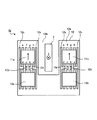
図6は、本実施の形態に係る電流センサ1bの構成例を示す平面模式図である。図6に示されるように、電流センサ1bは、被測定電流Iが通流する電流線2の周囲に配置された略直方体状の第1磁気検出素子11a及び第2磁気検出素子11bと、主表面に第1磁気検出素子11a及び第2磁気検出素子11bが配置される薄板状の配線基板12とを含んで構成される。
FIG. 6 is a schematic plan view illustrating a configuration example of the
第1磁気検出素子11a及び第2磁気検出素子11bの構成は、電流センサ1aの場合と同様である。
The configuration of the first
配線基板12の構成も電流センサ1aの場合と概ね同じである。ただし、本実施の形態に係る電流センサ1bは、配線基板12の第1主表面12aに、端子b、cに近接する導電パターン12cが設けられている。具体的には、導電パターン12cは、第1磁気検出素子11aの端子cの外側領域(電流線2と反対の領域)と、端子bの内側領域(電流線2側の領域)、及び第2磁気検出素子11bの端子bの外側領域(電流線2と反対の領域)と、端子cの内側領域(電流線2側の領域)に配置されている。また、導電パターン12cは端子a、dに接続されると共に、接地されている。このため、導電パターン12cがシールドとなって電磁ノイズをさらに低減できる。なお、導電パターン12cは、固定電位に接続されていれば接地されていなくとも良い。さらに、導電パターン12cと端子a、dとは接続されていなくても良い。
The configuration of the
配線基板12には、制御回路素子13a、13bが配置されている。第1磁気検出素子11a及び第2磁気検出素子11bの端子b、cは、配線パターン12dを介して制御回路素子13a、13bの端子と接続されている。
以上のように、本実施の形態の電流センサ1bは、第1磁気検出素子11a及び第2磁気検出素子11bの端子a、dと、端子b、cに近接する導電パターン12cとを有することにより、2つの端子b、cにおける電磁ノイズをさらに低減できる。このため、電流測定精度の低下をさらに抑制可能である。
As described above, the
本実施の形態は、他の実施の形態に示される構成と適宜組み合わせて実施可能である。 This embodiment can be implemented in appropriate combination with the structures described in the other embodiments.
(実施の形態3)
本実施の形態では、上述した実施の形態とは異なる構成の電流センサについて説明する。以下において、特に相違点についてのみ説明し、繰り返しの説明は省略する。また、上述した実施の形態と同一の構成については同一の符号を用いる。
(Embodiment 3)
In this embodiment, a current sensor having a configuration different from that of the above-described embodiment will be described. In the following, only the differences will be described, and repeated description will be omitted. Moreover, the same code | symbol is used about the same structure as embodiment mentioned above.
図7は、本実施の形態に係る電流センサ1cの構成例を示す平面模式図である。図7に示されるように、電流センサ1cは、被測定電流Iが通流する電流線2の周囲に配置された略直方体状の第1磁気検出素子11a及び第2磁気検出素子11bと、主表面に第1磁気検出素子11a及び第2磁気検出素子11bが配置される薄板状の配線基板12とを含んで構成される。
FIG. 7 is a schematic plan view illustrating a configuration example of the current sensor 1c according to the present embodiment. As shown in FIG. 7, the current sensor 1c includes a substantially rectangular parallelepiped first
第1磁気検出素子11a及び第2磁気検出素子11bの構成は、電流センサ1aの場合と同様である。配線基板12の構成は電流センサ1bの場合と概ね同じである。
The configuration of the first
配線基板12の構成は電流センサ1bの場合と概ね同じである。ただし、電流センサ1cの導電パターン12eは、第1磁気検出素子11aの端子bより端子cに近接して配置されている。すなわち、導電パターン12eと第1磁気検出素子11aの外側面(電流線2と反対の側面)との距離は、導電パターン12eと第1磁気検出素子11aの内側面(電流線2寄りの側面)との距離より小さくなっている。導電パターン12eは、第1磁気検出素子11bの端子cより端子bに近接して配置されている。すなわち、導電パターン12eと第2磁気検出素子11bの外側面(電流線2と反対の側面)との距離は、導電パターン12eと第2磁気検出素子11bの内側面(電流線2寄りの側面)との距離より小さくなっている。
The configuration of the
このように、電流線2との距離が大きい出力端子と導電パターン12eとの距離を、電流線2との距離が小さい出力端子と導電パターン12eとの距離より小さくすることで、出力端子である端子b、cにおける電流線2からの電磁ノイズを均質化できる。このため、2つの出力の差をとることで電磁ノイズをキャンセルし、電流測定精度の低下をさらに抑制可能である。
In this way, the distance between the output terminal having a large distance to the current line 2 and the
また、導電パターン12eは、出力端子である端子b、cを囲むように配置されている。導電パターン12eが端子b、cを囲むことで、電流線2からの電磁ノイズをさらに低減できる。
The
以上のように、本実施の形態の電流センサ1cは、第1磁気検出素子11a及び第2磁気検出素子11bの端子a、dと、端子a、dに近接する導電パターン12eとを有することにより、2つの端子b、cにおける電磁ノイズをさらに低減できる。また、端子b、cと導電パターン12eとの距離や、導電パターン12eの形状を制御することにより、電磁ノイズを低減し、電流測定精度の低下をさらに抑制可能である。
As described above, the current sensor 1c according to the present embodiment includes the terminals a and d of the first
本実施の形態は、他の実施の形態に示される構成と適宜組み合わせて実施可能である。 This embodiment can be implemented in appropriate combination with the structures described in the other embodiments.
(実施の形態4)
本実施の形態では、上述した実施の形態とは異なる構成の電流センサについて説明する。以下において、特に相違点についてのみ説明し、繰り返しの説明は省略する。また、上述した実施の形態と同一の構成については同一の符号を用いる。
(Embodiment 4)
In this embodiment, a current sensor having a configuration different from that of the above-described embodiment will be described. In the following, only the differences will be described, and repeated description will be omitted. Moreover, the same code | symbol is used about the same structure as embodiment mentioned above.
図8は、本実施の形態に係る電流センサ1dの構成例を示す模式図である。図8Aは電流センサ1dの平面図であり、図8Bは電流センサ1dのAA´断面図であり、図8Cは電流センサ1dのBB´断面図である。図8Aに示されるように、電流センサ1dは、被測定電流Iが通流する電流線2の周囲に配置された略直方体状の第1磁気検出素子11a及び第2磁気検出素子11bと、主表面に第1磁気検出素子11a及び第2磁気検出素子11bが配置される薄板状の配線基板12とを含んで構成される。
FIG. 8 is a schematic diagram illustrating a configuration example of the current sensor 1d according to the present embodiment. 8A is a plan view of the current sensor 1d, FIG. 8B is an AA ′ sectional view of the current sensor 1d, and FIG. 8C is a BB ′ sectional view of the current sensor 1d. As shown in FIG. 8A, the current sensor 1d includes a first
第1磁気検出素子11a及び第2磁気検出素子11bの構成は、電流センサ1aの場合と同様である。
The configuration of the first
配線基板12の構成は電流センサ1cの場合と概ね同じである。ただし、図8B、Cに示されるように、導電パターン12fの一部は、配線基板12の側面に設けられている。例えば、第1磁気検出素子11a及び第2磁気検出素子11bの電流線2側の領域において、導電パターン12fは第1主表面12a及び側面に設けられている。また、第1磁気検出素子11a及び第2磁気検出素子11bの電流線2とは反対側の領域において、導電パターン12fは側面のみに設けられている。これにより、第1主表面12aにおける導電パターン12の占める面積を低減できるため、導電パターン12fを第1主表面12aのみに設ける場合と比較して、配線基板12のサイズを小さくできる。つまり、電流センサを小型化可能である。
The configuration of the
以上のように、本実施の形態の電流センサ1dは、第1磁気検出素子11a及び第2磁気検出素子11bの端子a、dと、端子a、dに近接する導電パターン12fとを有することにより、2つの端子b、cにおける電磁ノイズをさらに低減できる。また、端子b、cと導電パターン12fとの距離や、導電パターン12fの形状を制御することにより、電磁ノイズを低減し、電流測定精度の低下をさらに抑制可能である。また、導電パターン12fの一部を配線基板12の側面に設けることで、電流センサの小型化が可能である。
As described above, the current sensor 1d according to the present embodiment includes the terminals a and d of the first
本実施の形態は、他の実施の形態に示される構成と適宜組み合わせて実施可能である。 This embodiment can be implemented in appropriate combination with the structures described in the other embodiments.
このように、本発明の電流センサは、磁気検出素子の出力端子と電流線との間に配置されて固定電位が与えられるシールド端子により電流線からの電磁波がシールドされるため、出力端子における電磁ノイズを低減できる。このため、電流線の電圧変動などによって電磁波が発生しても電流測定精度の低下を抑制可能である。 As described above, the current sensor of the present invention shields electromagnetic waves from the current line by the shield terminal that is disposed between the output terminal of the magnetic detection element and the current line and is given a fixed potential. Noise can be reduced. For this reason, even if electromagnetic waves are generated due to voltage fluctuations of the current lines, it is possible to suppress a decrease in current measurement accuracy.
なお、本発明は上記実施の形態に限定されず、種々変更して実施することができる。例えば、上記実施の形態では2つの磁気センサを用いているが、3つ以上の磁気センサを用いることも可能である。 In addition, this invention is not limited to the said embodiment, A various change can be implemented. For example, although two magnetic sensors are used in the above embodiment, it is possible to use three or more magnetic sensors.
また、上記実施の形態における各素子の接続関係、大きさなどは、発明の趣旨を変更しない限りにおいて変更可能である。また、上記実施の形態に示す構成、方法などは、適宜組み合わせて実施可能である。その他、本発明は、本発明の範囲を逸脱しないで適宜変更して実施できる。 Further, the connection relationship, size, and the like of each element in the above embodiment can be changed without changing the gist of the invention. In addition, the structures, methods, and the like described in the above embodiments can be combined as appropriate. In addition, the present invention can be implemented with appropriate modifications without departing from the scope of the present invention.
本発明の電流センサは、例えば、電気自動車やハイブリッドカーなどのモータ駆動用電流の大きさを検知するために用いることが可能である。 The current sensor of the present invention can be used, for example, to detect the magnitude of a current for driving a motor of an electric vehicle or a hybrid car.
1a、1b、1c、1d 電流センサ
11a 第1磁気検出素子
11b 第2磁気検出素子
12 配線基板
13a、13b 制御回路素子
14 演算部
a、b、c、d、e、f、g、h 端子
M1、M2、M3、M4 磁気抵抗効果素子
1a, 1b, 1c, 1d
Claims (10)
前記シールド端子は、前記出力端子と前記電流線との間に設けられ固定電位が与えられることを特徴とする電流センサ。 A wiring board arranged so that the main surface is substantially orthogonal to the extending direction of the current line through which the current to be measured flows, and the wiring board are arranged on the main surface of the wiring board and are approximately the magnitude of the magnetic field at the arrangement position. A magnetic detection element having an output terminal that gives a proportional output and a shield terminal that shields electromagnetic waves from the current line to the output terminal;
The current sensor according to claim 1, wherein the shield terminal is provided between the output terminal and the current line, and is provided with a fixed potential.
前記切り欠き部に収容された前記電流線を挟むように2つの前記磁気検出素子が配置されたことを特徴とする請求項1から請求項9のいずれかに記載の電流センサ。
The wiring board has a notch for accommodating the current line,
10. The current sensor according to claim 1, wherein the two magnetic detection elements are disposed so as to sandwich the current line accommodated in the notch.
Priority Applications (1)
| Application Number | Priority Date | Filing Date | Title |
|---|---|---|---|
| JP2011094928A JP2012225818A (en) | 2011-04-21 | 2011-04-21 | Current sensor |
Applications Claiming Priority (1)
| Application Number | Priority Date | Filing Date | Title |
|---|---|---|---|
| JP2011094928A JP2012225818A (en) | 2011-04-21 | 2011-04-21 | Current sensor |
Publications (1)
| Publication Number | Publication Date |
|---|---|
| JP2012225818A true JP2012225818A (en) | 2012-11-15 |
Family
ID=47276142
Family Applications (1)
| Application Number | Title | Priority Date | Filing Date |
|---|---|---|---|
| JP2011094928A Withdrawn JP2012225818A (en) | 2011-04-21 | 2011-04-21 | Current sensor |
Country Status (1)
| Country | Link |
|---|---|
| JP (1) | JP2012225818A (en) |
Cited By (1)
| Publication number | Priority date | Publication date | Assignee | Title |
|---|---|---|---|---|
| CN104297548A (en) * | 2013-07-16 | 2015-01-21 | 横河电机株式会社 | Current sensor |
-
2011
- 2011-04-21 JP JP2011094928A patent/JP2012225818A/en not_active Withdrawn
Cited By (2)
| Publication number | Priority date | Publication date | Assignee | Title |
|---|---|---|---|---|
| CN104297548A (en) * | 2013-07-16 | 2015-01-21 | 横河电机株式会社 | Current sensor |
| US9459293B2 (en) | 2013-07-16 | 2016-10-04 | Yokogawa Electric Corporation | Current sensor |
Similar Documents
| Publication | Publication Date | Title |
|---|---|---|
| WO2013005459A1 (en) | Current sensor | |
| JP5531215B2 (en) | Current sensor | |
| JP6651956B2 (en) | Current sensor | |
| JP5659389B2 (en) | Current sensor | |
| US20130057273A1 (en) | Current sensor | |
| JP5906488B2 (en) | Current sensor | |
| JP2007078418A (en) | Current sensor and current sensing method | |
| JP5500956B2 (en) | Current detector | |
| WO2012046547A1 (en) | Current sensor | |
| JP2012018024A (en) | Current sensor | |
| US9335349B2 (en) | Current sensor | |
| JP5688572B2 (en) | Current sensor | |
| JP2015036636A (en) | Current sensor | |
| WO2013038867A1 (en) | Electric-current sensor | |
| JP2012026966A (en) | Current sensor | |
| JP5487403B2 (en) | Current sensor | |
| JP6265419B2 (en) | Magnetic detection device, current sensor, and magnetic detection method | |
| JP2013113630A (en) | Current detector | |
| JP5704347B2 (en) | Current sensor | |
| JP2012052980A (en) | Current sensor | |
| JP2012225818A (en) | Current sensor | |
| JP5504483B2 (en) | Current sensor | |
| JP2012242082A (en) | Current sensor | |
| JP5703470B2 (en) | Current sensor | |
| JP5504488B2 (en) | Current sensor |
Legal Events
| Date | Code | Title | Description |
|---|---|---|---|
| RD02 | Notification of acceptance of power of attorney |
Free format text: JAPANESE INTERMEDIATE CODE: A7422 Effective date: 20130620 |
|
| RD04 | Notification of resignation of power of attorney |
Free format text: JAPANESE INTERMEDIATE CODE: A7424 Effective date: 20131122 |
|
| A521 | Written amendment |
Free format text: JAPANESE INTERMEDIATE CODE: A523 Effective date: 20131220 |
|
| A300 | Withdrawal of application because of no request for examination |
Free format text: JAPANESE INTERMEDIATE CODE: A300 Effective date: 20140701 |