JP2012215852A - Image processing method and display device - Google Patents
Image processing method and display device Download PDFInfo
- Publication number
- JP2012215852A JP2012215852A JP2012062922A JP2012062922A JP2012215852A JP 2012215852 A JP2012215852 A JP 2012215852A JP 2012062922 A JP2012062922 A JP 2012062922A JP 2012062922 A JP2012062922 A JP 2012062922A JP 2012215852 A JP2012215852 A JP 2012215852A
- Authority
- JP
- Japan
- Prior art keywords
- image
- light
- image data
- conductive film
- objects
- Prior art date
- Legal status (The legal status is an assumption and is not a legal conclusion. Google has not performed a legal analysis and makes no representation as to the accuracy of the status listed.)
- Withdrawn
Links
Images
Classifications
-
- H—ELECTRICITY
- H04—ELECTRIC COMMUNICATION TECHNIQUE
- H04N—PICTORIAL COMMUNICATION, e.g. TELEVISION
- H04N13/00—Stereoscopic video systems; Multi-view video systems; Details thereof
- H04N13/10—Processing, recording or transmission of stereoscopic or multi-view image signals
- H04N13/106—Processing image signals
- H04N13/122—Improving the three-dimensional [3D] impression of stereoscopic images by modifying image signal contents, e.g. by filtering or adding monoscopic depth cues
-
- G—PHYSICS
- G06—COMPUTING OR CALCULATING; COUNTING
- G06T—IMAGE DATA PROCESSING OR GENERATION, IN GENERAL
- G06T19/00—Manipulating three-dimensional [3D] models or images for computer graphics
- G06T19/20—Editing of three-dimensional [3D] images, e.g. changing shapes or colours, aligning objects or positioning parts
-
- G—PHYSICS
- G09—EDUCATION; CRYPTOGRAPHY; DISPLAY; ADVERTISING; SEALS
- G09G—ARRANGEMENTS OR CIRCUITS FOR CONTROL OF INDICATING DEVICES USING STATIC MEANS TO PRESENT VARIABLE INFORMATION
- G09G3/00—Control arrangements or circuits, of interest only in connection with visual indicators other than cathode-ray tubes
- G09G3/001—Control arrangements or circuits, of interest only in connection with visual indicators other than cathode-ray tubes using specific devices not provided for in groups G09G3/02 - G09G3/36, e.g. using an intermediate record carrier such as a film slide; Projection systems; Display of non-alphanumerical information, solely or in combination with alphanumerical information, e.g. digital display on projected diapositive as background
- G09G3/003—Control arrangements or circuits, of interest only in connection with visual indicators other than cathode-ray tubes using specific devices not provided for in groups G09G3/02 - G09G3/36, e.g. using an intermediate record carrier such as a film slide; Projection systems; Display of non-alphanumerical information, solely or in combination with alphanumerical information, e.g. digital display on projected diapositive as background to produce spatial visual effects
-
- G—PHYSICS
- G09—EDUCATION; CRYPTOGRAPHY; DISPLAY; ADVERTISING; SEALS
- G09G—ARRANGEMENTS OR CIRCUITS FOR CONTROL OF INDICATING DEVICES USING STATIC MEANS TO PRESENT VARIABLE INFORMATION
- G09G5/00—Control arrangements or circuits for visual indicators common to cathode-ray tube indicators and other visual indicators
- G09G5/003—Details of a display terminal, the details relating to the control arrangement of the display terminal and to the interfaces thereto
-
- H—ELECTRICITY
- H04—ELECTRIC COMMUNICATION TECHNIQUE
- H04N—PICTORIAL COMMUNICATION, e.g. TELEVISION
- H04N13/00—Stereoscopic video systems; Multi-view video systems; Details thereof
- H04N13/10—Processing, recording or transmission of stereoscopic or multi-view image signals
- H04N13/106—Processing image signals
- H04N13/139—Format conversion, e.g. of frame-rate or size
-
- H—ELECTRICITY
- H04—ELECTRIC COMMUNICATION TECHNIQUE
- H04N—PICTORIAL COMMUNICATION, e.g. TELEVISION
- H04N13/00—Stereoscopic video systems; Multi-view video systems; Details thereof
- H04N13/10—Processing, recording or transmission of stereoscopic or multi-view image signals
- H04N13/106—Processing image signals
- H04N13/156—Mixing image signals
-
- H—ELECTRICITY
- H04—ELECTRIC COMMUNICATION TECHNIQUE
- H04N—PICTORIAL COMMUNICATION, e.g. TELEVISION
- H04N13/00—Stereoscopic video systems; Multi-view video systems; Details thereof
- H04N13/30—Image reproducers
- H04N13/302—Image reproducers for viewing without the aid of special glasses, i.e. using autostereoscopic displays
- H04N13/31—Image reproducers for viewing without the aid of special glasses, i.e. using autostereoscopic displays using parallax barriers
-
- H—ELECTRICITY
- H04—ELECTRIC COMMUNICATION TECHNIQUE
- H04N—PICTORIAL COMMUNICATION, e.g. TELEVISION
- H04N13/00—Stereoscopic video systems; Multi-view video systems; Details thereof
- H04N13/30—Image reproducers
- H04N13/332—Displays for viewing with the aid of special glasses or head-mounted displays [HMD]
- H04N13/341—Displays for viewing with the aid of special glasses or head-mounted displays [HMD] using temporal multiplexing
-
- G—PHYSICS
- G06—COMPUTING OR CALCULATING; COUNTING
- G06T—IMAGE DATA PROCESSING OR GENERATION, IN GENERAL
- G06T2219/00—Indexing scheme for manipulating 3D models or images for computer graphics
- G06T2219/20—Indexing scheme for editing of 3D models
- G06T2219/2016—Rotation, translation, scaling
-
- G—PHYSICS
- G09—EDUCATION; CRYPTOGRAPHY; DISPLAY; ADVERTISING; SEALS
- G09G—ARRANGEMENTS OR CIRCUITS FOR CONTROL OF INDICATING DEVICES USING STATIC MEANS TO PRESENT VARIABLE INFORMATION
- G09G2340/00—Aspects of display data processing
- G09G2340/04—Changes in size, position or resolution of an image
- G09G2340/0464—Positioning
-
- H—ELECTRICITY
- H04—ELECTRIC COMMUNICATION TECHNIQUE
- H04N—PICTORIAL COMMUNICATION, e.g. TELEVISION
- H04N13/00—Stereoscopic video systems; Multi-view video systems; Details thereof
- H04N2013/0074—Stereoscopic image analysis
- H04N2013/0081—Depth or disparity estimation from stereoscopic image signals
Landscapes
- Engineering & Computer Science (AREA)
- Multimedia (AREA)
- Signal Processing (AREA)
- Physics & Mathematics (AREA)
- Computer Hardware Design (AREA)
- General Physics & Mathematics (AREA)
- Theoretical Computer Science (AREA)
- Computer Graphics (AREA)
- Architecture (AREA)
- General Engineering & Computer Science (AREA)
- Software Systems (AREA)
- Control Of Indicators Other Than Cathode Ray Tubes (AREA)
- Electroluminescent Light Sources (AREA)
- Controls And Circuits For Display Device (AREA)
- Image Processing (AREA)
- Image Analysis (AREA)
- Devices For Indicating Variable Information By Combining Individual Elements (AREA)
- Control Of El Displays (AREA)
Abstract
【課題】画像の立体感、奥行き感を高める画像処理方法と、上記画像処理方法を利用した表示装置とを提供する。
【解決手段】画像の画像データから複数の対象物の画像データと、背景の画像データとを分離する。そして、各対象物の画像データから特徴量を取得し、対象物の識別を行う。次いで、画像中における対象物の大きさと、データベース中に登録されている対象物の大きさとから、観察者の視点と各対象物との相対的な距離を定める。次いで、上記相対的な距離が短い対象物ほど大きくなるように、個々の対象物の画像データに画像処理を施す。次いで、画像処理を施した対象物の画像データと、背景の画像データとを合成することで、画像の奥行き感、或いは立体感を高める。
【選択図】図1An image processing method for enhancing the stereoscopic effect and depth of an image and a display device using the image processing method are provided.
Image data of a plurality of objects and background image data are separated from the image data of the image. And the feature-value is acquired from the image data of each target object, and a target object is identified. Next, a relative distance between the observer's viewpoint and each object is determined from the size of the object in the image and the size of the object registered in the database. Next, image processing is performed on the image data of each object so that the object with the shorter relative distance becomes larger. Next, by combining the image data of the object subjected to the image processing and the background image data, the sense of depth or stereoscopic effect of the image is enhanced.
[Selection] Figure 1
Description
本発明は、画像処理方法と、上記画像処理方法を利用した表示装置に関する。 The present invention relates to an image processing method and a display device using the image processing method.
三次元画像に対応した表示装置の市場が拡大傾向にある。三次元画像の表示は、両眼で立体の対象物を見たときに生ずるであろう、両眼間の網膜像の差異(両眼視差)を表示装置において作為的に作り出すことで、行うことができる。上記両眼視差を利用した三次元画像用の表示装置は、各種の表示方式が開発され商品化されているが、主に、パララックスバリア、レンチキュラーレンズ、マイクロレンズアレイなどの光学系を利用した直視タイプの表示方式と、シャッター付きの眼鏡を利用した表示方式とに分類される。 The market for display devices that support 3D images is on the rise. 3D image display is performed by creating a difference in the retinal image (binocular parallax) between the eyes, which would occur when viewing a stereoscopic object with both eyes, on the display device. Can do. Various display methods have been developed and commercialized for the above three-dimensional image display devices using binocular parallax, but mainly using an optical system such as a parallax barrier, a lenticular lens, and a microlens array. It is classified into a direct-view type display method and a display method using glasses with a shutter.
下記の特許文献1には、パララックスバリアを用いることで、右眼には右眼用の画像が、左眼には左眼用の画像が映るようにし、三次元画像を表示する技術について開示されている。また、下記の特許文献2には、眼鏡を用いて三次元画像の表示を行う液晶表示装置について記載されている。 Patent Document 1 below discloses a technique for displaying a three-dimensional image by using a parallax barrier so that an image for the right eye appears in the right eye and an image for the left eye in the left eye. Has been. Patent Document 2 below describes a liquid crystal display device that displays a three-dimensional image using glasses.
パララックスバリア、レンチキュラーレンズ、マイクロレンズアレイなどの光学系を利用した三次元画像の表示方式では、右眼に対応した画素からの光を右眼に、左眼に対応した画素からの光を左眼に入射させる。よって、画素部の水平方向において、画像の表示に寄与する画素数が実際の画素数の半分となるため、高精細な画像の表示が妨げられる。 In a 3D image display method using an optical system such as a parallax barrier, lenticular lens, or microlens array, light from the pixel corresponding to the right eye is to the right eye, and light from the pixel corresponding to the left eye is to the left Make it enter the eye. Therefore, in the horizontal direction of the pixel portion, the number of pixels contributing to image display is half of the actual number of pixels, and display of a high-definition image is hindered.
また、眼鏡を利用した三次元画像の表示方式では、画面において左眼用画像と右眼用画像を交互に表示し、それらをシャッター付きの眼鏡を通して見ることにより、人間の眼に三次元画像を認識させる。よって、二次元画像の表示を行う場合に比べ、1フレーム期間における画素部への画像の書き込み回数が増大するので、高い周波数での駆動が可能な高スペックの駆動回路が必要となる他、表示装置全体の消費電力も高まる。 Also, in the 3D image display method using glasses, the left-eye image and the right-eye image are alternately displayed on the screen, and the 3D image is displayed on the human eye by looking through the glasses with the shutter. Recognize. Therefore, compared with the case of displaying a two-dimensional image, the number of times of image writing to the pixel portion in one frame period is increased, so that a high-spec drive circuit that can be driven at a high frequency is required. The power consumption of the entire device is also increased.
上述の課題に鑑み、本発明の一態様では、1フレーム期間における画素部への画像の書き込み回数を小さく抑えつつ、或いは、画像の表示に寄与する画素数が少なくなるのを抑えつつ、画像の立体感、奥行き感を高める画像処理方法と、上記画像処理方法を利用した表示装置とを提供する。 In view of the above problems, according to one embodiment of the present invention, the number of times that an image is written to a pixel portion in one frame period is reduced or the number of pixels that contribute to image display is reduced. Provided are an image processing method for enhancing a three-dimensional feeling and a depth feeling, and a display device using the image processing method.
本発明の一態様では、二次元画像の中に対象物が複数存在している場合、一の対象物を他の対象物よりも大きくすることで、上記一の対象物が他の対象物よりも手前に位置するように見えるという、人間の奥行きに対する知覚の特性を利用する。 In one embodiment of the present invention, when a plurality of objects are present in a two-dimensional image, the one object is made larger than the other objects so that the one object is more than the other objects. It uses the characteristic of perception of human depth that it seems to be located in front.
具体的に、本発明の一態様に係る画像処理方法では、画像データを複数の対象物の画像データと、背景の画像データとに分離する。そして、各対象物の画像データから特徴量を取得する。特徴量とは、対象物を物体認識する上で有用な特徴を数値化したものであり、特徴量により対象物の識別が可能となる。例えば、対象物の形状、色、階調、テクスチャなどから得られる特徴量を、対象物の識別に用いることができる。そして、上記特徴量と、データベース中に蓄積されている、モデルとなる対象物の特徴量に関連づけられた、当該モデルとなる対象物の大きさのデータとを照合することで、各対象物の大きさのデータを得ることができる。そして、データベースから得られた上記各対象物の大きさのデータと、画像中における対象物どうしの相対的な大きさとから、観察者の視点と各対象物との間の相対的な距離、或いは対象物どうしの前後関係を定めることができる。次いで、上記相対的な距離が短い対象物ほど、或いは前に位置する対象物ほど大きくなるように、個々の対象物の画像データに画像処理を施す。次いで、画像処理を施した対象物の画像データと、背景の画像データとを合成することで、画像の奥行き感、或いは立体感が高められた画像データを得る。 Specifically, in the image processing method according to an aspect of the present invention, the image data is separated into a plurality of object image data and background image data. And the feature-value is acquired from the image data of each target object. The feature amount is a numerical value of a feature useful for recognizing an object, and the object can be identified by the feature amount. For example, feature quantities obtained from the shape, color, gradation, texture, etc. of the object can be used for identifying the object. Then, by comparing the feature amount with the data of the size of the target object that is associated with the feature amount of the target object that is stored in the database, Size data can be obtained. Then, from the data of the size of each object obtained from the database and the relative size of the objects in the image, the relative distance between the observer's viewpoint and each object, or The context between objects can be defined. Next, image processing is performed on the image data of each object so that the object with the shorter relative distance or the object positioned in front becomes larger. Next, the image data of the object subjected to the image processing and the image data of the background are combined to obtain image data with an enhanced sense of depth or stereoscopic effect.
さらに、本発明の一態様では、二次元画像の中に対象物が複数存在している場合、一の対象物の輪郭を他の対象物の輪郭よりも強調することで、上記対象物が他の対象物よりも手前に位置するように見えるという、人間の奥行きに対する知覚の特性を利用する。 Furthermore, in one embodiment of the present invention, when there are a plurality of objects in a two-dimensional image, the object is enhanced by enhancing the outline of one object more than the outline of another object. It uses the characteristic of perception of human depth that it appears to be in front of the target object.
具体的に、本発明の一態様に係る画像処理方法では、上述した画像処理方法と同様に、観察者の視点と各対象物との相対的な距離、或いは対象物どうしの前後関係を定めた後、上記相対的な距離が短い対象物ほど、或いは前に位置する対象物ほど、その輪郭が強調されるように、個々の対象物の画像データに画像処理を施す。次いで、上述した画像処理方法と同様に、画像処理を施した対象物の画像データと、背景の画像データとを合成することで、画像の奥行き感、或いは立体感が高められた画像データを得る。 Specifically, in the image processing method according to one aspect of the present invention, as in the image processing method described above, the relative distance between the observer's viewpoint and each object or the front-to-back relationship between objects is determined. Thereafter, image processing is performed on the image data of each object so that the object with a shorter relative distance or the object positioned in front of the object is emphasized. Next, similarly to the image processing method described above, the image data of the object subjected to the image processing and the image data of the background are combined to obtain image data with an enhanced sense of depth or stereoscopic effect. .
さらに、本発明の一態様では、二次元画像の中に対象物が複数存在している場合、二次元画像の中に一の消失点があると仮定し、一の対象物を上記消失点から離すことで、上記対象物が他の対象物よりも手前に位置するように見えるという、人間の奥行きに対する知覚の特性を利用しても良い。 Furthermore, in one aspect of the present invention, when there are a plurality of objects in the two-dimensional image, it is assumed that there is one vanishing point in the two-dimensional image, and one object is removed from the vanishing point. It is also possible to use the characteristic of perception with respect to human depth that the object appears to be positioned in front of other objects by separating them.
具体的に、本発明の一態様に係る画像処理方法では、上述した画像処理方法と同様に、個々の対象物の画像データに画像処理を施した後、観察者の視点との間の相対的な距離が短い対象物ほど、或いは前に位置する対象物ほど、画像の中の消失点から離れるようにその位置を移動させ、画像処理を施した対象物の画像データと、背景の画像データとを合成することで、画像の奥行き感、或いは立体感が高められた画像データを得ても良い。 Specifically, in the image processing method according to one aspect of the present invention, as in the image processing method described above, after image processing is performed on the image data of each target object, The shorter the target distance, or the earlier the target object, the position is moved away from the vanishing point in the image, and the image data of the target object subjected to image processing, the background image data, By combining the image data, image data in which a sense of depth or a stereoscopic effect of the image is enhanced may be obtained.
本発明の一態様に係る画像処理方法、表示装置では、両眼視差を利用する表示方式のように、両眼に与えられる画像情報の差異により立体感、或いは奥行き感を得るものではない。すなわち、上述した画像処理方法、表示装置では、形成された画像を単眼に視覚として与えた場合でも、人間は立体感、或いは奥行き感を得ることができる。よって、本発明の一態様では、両眼視差を利用する表示方式のように、右眼用の画像と左眼用の画像を順に、或いは同時に表示する必要がないので、1フレーム期間における画素部への画像の書き込み回数を小さく抑えつつ、或いは、画像の表示に寄与する画素数が少なくなるのを抑えつつ、画像の立体感、奥行き感を高めることができる。 In the image processing method and display device according to one embodiment of the present invention, unlike the display method using binocular parallax, a stereoscopic effect or a sense of depth is not obtained due to a difference in image information given to both eyes. That is, in the above-described image processing method and display device, even when the formed image is given to a single eye as a vision, a human can obtain a three-dimensional effect or a sense of depth. Therefore, in one embodiment of the present invention, unlike the display method using binocular parallax, it is not necessary to display an image for the right eye and an image for the left eye in order or at the same time. It is possible to increase the stereoscopic effect and depth of the image while suppressing the number of times the image is written to the image or reducing the number of pixels contributing to image display.
以下では、本発明の実施の形態について図面を用いて詳細に説明する。ただし、本発明は以下の説明に限定されず、本発明の趣旨及びその範囲から逸脱することなくその形態及び詳細を様々に変更し得ることは、当業者であれば容易に理解される。したがって、本発明は、以下に示す実施の形態の記載内容に限定して解釈されるものではない。 Hereinafter, embodiments of the present invention will be described in detail with reference to the drawings. However, the present invention is not limited to the following description, and it will be easily understood by those skilled in the art that modes and details can be variously changed without departing from the spirit and scope of the present invention. Therefore, the present invention should not be construed as being limited to the description of the embodiments below.
(実施の形態1)
本発明の一態様に係る表示装置について、図1を用いて説明する。
(Embodiment 1)
A display device according to one embodiment of the present invention will be described with reference to FIGS.
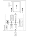
図1に示すように、本発明の一態様に係る表示装置100は、表示装置100に入力された画像データ103に画像処理を施し、画像信号を生成する画像処理部101と、上記画像信号に従って画像の表示を行う表示部102とを有する。
As shown in FIG. 1, a display device 100 according to one embodiment of the present invention performs image processing on
図1に示す画像処理部101は、制御装置104、演算装置105、入力部106、緩衝記憶装置107、不揮発性記憶装置108、表示部用コントローラ109などを有する。
An
制御装置104は、画像処理部101が有する演算装置105、入力部106、緩衝記憶装置107、不揮発性記憶装置108、表示部用コントローラ109の動作を統括的に制御する回路である。
The
演算装置105は、論理演算、四則演算など各種の演算処理を行う論理回路である。
The
入力部106は、表示装置100に入力された画像データ103のフォーマットを、表示装置100で扱うフォーマットに変換する、インターフェースである。
The
不揮発性記憶装置108は、データベース110を有する。データベース110は、対象物の識別(物体認識)に用いられる特徴量と、モデルとなる対象物の大きさのデータとが関連づけられた、データの集合体である。さらに、不揮発性記憶装置108は、演算装置105における演算処理に用いられる各種データや、制御装置104において実行される命令などが記憶されている。
The
緩衝記憶装置107は、各種データを一時的に記憶する機能を有する。具体的に、緩衝記憶装置107は、使用頻度の高いデータを一時的に記憶しておくデータキャッシュと、制御装置104に送られる命令(プログラム)のうち、使用頻度の高い命令を一時的に記憶しておく命令キャッシュと、制御装置104が次に実行する命令のアドレスを記憶するプログラムカウンタと、制御装置104が次に実行する命令を記憶する命令レジスタと、不揮発性記憶装置108から読み出されたデータ、演算装置105の演算処理の途中で得られたデータ、或いは演算装置105の演算処理の結果得られたデータなどを記憶するレジスタファイルと、を有していても良い。
The
制御装置104は、緩衝記憶装置107から入力された命令をデコードし、デコードされた命令に従って、演算装置105、入力部106、緩衝記憶装置107、不揮発性記憶装置108、表示部用コントローラ109の動作を統括的に制御することで、画像処理部101に入力された画像データ103に、画像処理を施す。
The
表示部用コントローラ109は、画像処理が施された画像データ103を用い、表示部102の仕様に合った画像信号を生成する。生成された画像信号は、表示部102に供給される。また、表示部用コントローラ109は、表示部102の駆動を制御するためのクロック信号、スタートパルス信号などの駆動信号や、電源電位を、表示部102に供給する機能を有する。
The
表示部102は、画像信号を用いて画像の表示を行う画素部111と、画素部111の動作を制御する駆動回路112とを有する。表示部102には、液晶表示装置、有機発光素子(OLED)などの発光素子を備えた発光装置、電子ペーパー、DMD(Digital Micromirror Device)、PDP(Plasma Display Panel)、FED(Field Emission Display)等の、各画素の階調を制御することで画像の表示を行う装置を、用いることができる。
The display unit 102 includes a
次いで、図1に示した表示装置100において行われる、本発明の一態様に係る画像処理方法について説明する。 Next, an image processing method according to one embodiment of the present invention performed in the display device 100 illustrated in FIG. 1 will be described.
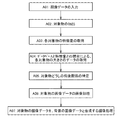
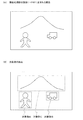
図2に、本発明の一態様に係る画像処理方法の流れを、フローチャートで一例として示す。まず、図2に示すように、画像処理部101に画像データ103が入力される(A01:画像データの入力)。図3(A)に、画像処理前の画像データ103に含まれる画像を、一例として示す。
FIG. 2 shows an example of a flow of an image processing method according to one embodiment of the present invention in a flowchart. First, as shown in FIG. 2,
画像データ103は、フルカラー画像に対応する画像データであっても良いし、モノカラー画像に対応した画像データであっても良い。画像データ103がフルカラー画像に対応する画像データである場合、画像データ103には、各色相に対応する複数の画像データが含まれている。
The
なお、本明細書では、異なる色相の色を複数用い、各色の階調により表示される画像をフルカラー画像とする。また、単一の色相の色を用い、その色の階調により表示される画像をモノカラー画像とする。 In the present specification, a plurality of colors having different hues are used, and an image displayed with the gradation of each color is a full-color image. Also, a single hue color is used, and an image displayed with the gradation of the color is a monocolor image.
画像処理部101では、入力された画像データ103から、画像データ103内に含まれる対象物の抽出を行う(A02:対象物の抽出)。対象物の抽出は、対象物が有する輪郭線の抽出により、行うことができる。対象物の抽出により、画像データ103は、対象物の画像データと、背景の画像データとに分離される。図3(B)に、図3(A)に示した画像データ103に含まれる画像から、対象物A、対象物B、対象物Cを抽出する例を示す。
The
次いで、抽出した各対象物について、特徴量の取得を行う(A03:各対象物の特徴量の取得)。特徴量とは、対象物を物体認識する上で有用な特徴を数値化したものであり、形状、色、階調、テクスチャなどから得られる特徴量を用いることができる。また、特徴量の取得は、公知の方法を用いることができる。例えば、形状から特徴量を取得する場合、対象物を縁取る輪郭線に含まれる特徴点を抽出し、当該特徴点の位置を特徴量として用いても良いし、対象物の構成要素の一つを縁取る輪郭線に含まれる特徴点を抽出し、当該特徴点の位置を特徴量として用いても良い。 Next, the feature amount is acquired for each extracted object (A03: acquisition of the feature amount of each object). The feature value is a numerical value of a feature useful for recognizing an object, and a feature value obtained from a shape, color, gradation, texture, or the like can be used. Also, a known method can be used to acquire the feature amount. For example, when acquiring a feature amount from a shape, a feature point included in a contour line that borders the object may be extracted, and the position of the feature point may be used as the feature amount, or one of the components of the object It is also possible to extract a feature point included in a contour line that borders and to use the position of the feature point as a feature amount.
なお、輪郭線が無数の輪郭点で構成されていると仮定した場合に、接線の傾きが急峻に変化する輪郭点を特徴点として抽出しても良い。或いは、接線の傾きが同程度の輪郭点が連続している場合に、上記輪郭点の一つを特徴点として抽出しても良い。 Note that when it is assumed that the contour line is composed of an infinite number of contour points, contour points at which the slope of the tangent line changes sharply may be extracted as feature points. Alternatively, when contour points having the same tangent slope are continuous, one of the contour points may be extracted as a feature point.
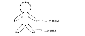
図5に、対象物Aと、対象物Aの輪郭線から抽出された複数の特徴点130とを示す。図5では、対象物Aの輪郭線を構成する輪郭点のうち、接線の傾きが急峻に変化する輪郭点を特徴点として抽出している場合を例示している。 FIG. 5 shows the object A and a plurality of feature points 130 extracted from the contour line of the object A. FIG. 5 illustrates a case where, out of the contour points constituting the contour line of the object A, a contour point whose tangent slope changes sharply is extracted as a feature point.
なお、対象物を物体認識する上で用いる特徴量は1つであっても良いし、複数であっても良い。複数の特徴量を用いて物体認識を行うことで、物体認識の精度を高めることができる。 Note that one or more feature quantities may be used for recognizing the target object. By performing object recognition using a plurality of feature amounts, the accuracy of object recognition can be increased.
次いで、各対象物について、得られた特徴量をデータベース110と照合することにより、各対象物の大きさのデータを取得する(A04:特徴量とデータベースとの照合による、各対象物の大きさのデータの取得)。例えば、対象物Aが人間であるとすると、その特徴量をデータベース110と照合することにより、人間の大きさのデータが取得できる。
Next, with respect to each object, the obtained feature value is collated with the
なお、複数の対象物が同一のものであると物体認識された場合でも、当該対象物の大きさが個体差を有する場合がある。対象物の大きさが個体差を有する場合は、大きさに幅を持たせたデータを、データベース110に用意しておいても良いし、平均化された大きさのデータを、データベース110に用意しておいても良い。
In addition, even when an object is recognized that a plurality of objects are the same, the size of the object may have individual differences. When the size of an object has individual differences, data with a wide range of sizes may be prepared in the
また、人間の想像の産物のように、対象物が実在しない場合であっても、上記対象物の大きさを設計者が適宜設定し、上記大きさのデータをデータベース110に用意しておくことが可能である。
Further, even if the object does not actually exist like a product imagined by human beings, the size of the object should be set appropriately by the designer, and data of the size should be prepared in the
また、データベース110に蓄積されている対象物の大きさのデータは、当該対象物全体の縦幅、横幅、または面積などのデータであっても良いし、当該対象物が有する構成要素の縦幅、横幅、または面積などのデータであっても良い。
Further, the data of the size of the target object stored in the
次いで、複数の各対象物についての大きさのデータが取得されたら、画像データ103内における各対象物の大きさと、上記取得された大きさのデータとから、対象物どうしの前後関係を特定する(A05:対象物どうしの前後関係の特定)。例えば、データベース110から得られた対象物の大きさD0に対する、画像データ103内における対象物の大きさD1の比率が大きい対象物ほど、他の対象物よりも前に位置するものと、決定することができる。
Next, when the size data for each of the plurality of objects is acquired, the context between the objects is specified from the size of each object in the
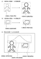
図3(B)に示した画像データの場合、上記D0に対するD1の比率が、対象物Aが最も大きく、対象物Cが最も小さい。よって、対象物Aが最も前に位置し、対象物Aの後ろに対象物Bが位置し、対象物Bの後ろに対象物Cが位置する。 In the case of the image data shown in FIG. 3B, the ratio of D 1 to D 0 is the largest for the object A and the smallest for the object C. Therefore, the object A is located at the forefront, the object B is located behind the object A, and the object C is located behind the object B.
なお、対象物どうしの前後関係を特定する際に、画像データ103が、観察者の視点から遠近法を用いて作成されたものと仮定して、観察者の視点と、各対象物の間の相対的な距離の比率を算出しても良い。観察者の視点の位置は、適宜設計者が定めることができる。
Note that when specifying the context between objects, it is assumed that the
次いで、画像データ103内における各対象物の画像データに画像処理を施すことで、前に位置する対象物の輪郭を強調し、前に位置する対象物の大きさを拡大する(A06:対象物の画像データの画像処理)。そして、輪郭の強調は、より前に位置する対象物ほど強くする。また、画像データ103内における対象物の大きさは、より前に位置する対象物ほど拡大する。
Next, image processing is performed on the image data of each object in the
図4(A)に、画像処理前の対象物Aと、画像処理後の対象物Aを例示する。図4(A)に示すように、画像処理により、対象物Aの輪郭が強調され、大きさが拡大される。また、図4(B)に、画像処理前の対象物Bと、画像処理後の対象物Bを例示する。図4(B)に示すように、画像処理により、対象物Bの輪郭が強調され、大きさが拡大される。ただし、対象物Bよりも手前に位置する対象物Aの方が、輪郭の強調を強く施され、また、その拡大率も大きい。 FIG. 4A illustrates an object A before image processing and an object A after image processing. As shown in FIG. 4A, the outline of the object A is emphasized and the size is enlarged by image processing. FIG. 4B illustrates an object B before image processing and an object B after image processing. As shown in FIG. 4B, the contour of the object B is emphasized and the size is enlarged by image processing. However, the object A located in front of the object B is more strongly emphasized by the contour, and the enlargement ratio is also larger.
上記輪郭の強調の度合いと、拡大率については、対象物の前後関係の順番に従って、予め設定しておくことができる。m個(mは2以上の自然数)の対象物が画像データ中に存在していて、なおかつ上記対象物が前後関係において互いに異なる位置に存在している場合の、各対象物の輪郭の強調の度合いと、拡大率について考察する。例えば、前からm番目の対象物、すなわち、最も後ろに位置する対象物の、輪郭の強調の度合い或いは拡大率を等倍とする。そして、前からm−1番目の対象物はt倍(tは1より大きい)、m−2番目の対象物はt2倍、m−3番目の対象物はt3倍というように、前に位置する対象物ほど、順にその輪郭の強調の度合い或いは拡大率を大きくしていく。上記構成の場合、前からn番目(nは2以上m以下の自然数)の対象物については、輪郭の強調の度合い或いは拡大率をt(m−n)倍とすれば良い。 The degree of enhancement of the contour and the enlargement ratio can be set in advance according to the order of the order of the objects. Emphasis on the contour of each object when m objects (m is a natural number of 2 or more) are present in the image data and the objects are present at different positions in the context. Consider the degree and magnification. For example, the degree of enhancement of the contour or the enlargement ratio of the mth object from the front, that is, the object located at the rearmost position is set to the same magnification. The m-1 th object from the front is t times (t is greater than 1), the m-2 th object is t 2 times, the m-3 th object is t 3 times, and so on. The degree of enhancement of the contour or the enlargement ratio is increased in order for the object located at. In the case of the above configuration, for the nth object (n is a natural number of 2 or more and m or less) from the front, the degree of enhancement of the contour or the enlargement ratio may be t (mn) times.
或いは、輪郭の強調の度合いと拡大率を、対象物と観察者の視点との間の相対的な距離から、定めても良い。 Alternatively, the degree of enhancement and the enlargement ratio of the contour may be determined from the relative distance between the object and the observer's viewpoint.
次いで、画像処理が施された各対象物の画像データを、背景の画像データと合成する画像処理を行う(A07:対象物の画像データを、背景の画像データと合成する画像処理)。本実施の形態では、対象物のうち、最も後ろに位置する対象物に対して、輪郭の強調や、大きさの拡大などの、立体視を得るための画像処理を施していないが、最も後ろに位置する対象物の画像データに対しても、上記画像処理を施しても良い。 Next, image processing for synthesizing the image data of each object subjected to image processing with background image data is performed (A07: image processing for synthesizing image data of the object with background image data). In the present embodiment, image processing for obtaining a stereoscopic view, such as contour enhancement or size enlargement, is not performed on the rearmost target among the targets, but the rearmost The above-described image processing may be performed also on the image data of the object located in the position.
画像処理を施していない対象物Cのデータ及び背景のデータと、図4(A)に示した画像処理後の対象物Aのデータと、図4(B)に示した画像処理後の対象物Bのデータとを、合成することで得られる画像データに含まれる画像を、図4(C)に示す。 Data of the object C not subjected to image processing and background data, data of the object A after the image processing shown in FIG. 4A, and object after the image processing shown in FIG. FIG. 4C shows an image included in the image data obtained by combining the B data.
上記画像処理方法により、画像の奥行き感、或いは立体感が高められた画像データを得ることができる。 By the image processing method, image data with enhanced depth or stereoscopic effect can be obtained.
なお、上述した(A06:対象物の画像データの画像処理)及び(A07:対象物の画像データを、背景の画像データと合成する画像処理)において、線形補間、最近傍補間などの公知の補間処理を用いても良い。 In the above-described (A06: Image processing of object image data) and (A07: Image processing for combining object image data with background image data), known interpolation such as linear interpolation and nearest neighbor interpolation is used. Processing may be used.
また、(A06:前に位置する対象物の画像データの画像処理)において、画像処理前の画像と、画像処理後の画像とは、相似の関係にある。本発明の一態様では、(A07:対象物の画像データを、背景の画像データと合成する画像処理)において、上記相似の中心が、画像処理前の対象物の内部に位置するように、画像処理後の対象物のデータと、背景の画像データとを合成するようにしても良いし、相似の中心が上記以外の場所に位置していても良い。 In (A06: Image processing of the image data of the object positioned in front), the image before the image processing and the image after the image processing have a similar relationship. In one embodiment of the present invention, in (A07: Image processing for combining image data of an object with background image data), the image is so positioned that the center of the similarity is located inside the object before image processing. The processed object data and the background image data may be combined, or the center of similarity may be located at a place other than the above.
後者の場合、例えば、画像処理前の画像データ103に含まれる画像中に、一の消失点があると仮定する。そして、画像処理後の対象物の中心点が、画像処理前の対象物の中心点と消失点とを結ぶ線上に存在し、なおかつ、画像処理後の対象物の中心点と消失点の間の距離が、画像処理前の対象物の中心点と消失点の間の距離よりも長くなるように、画像処理後の対象物の位置を定める。そして、前に位置する対象物ほど、画像処理前の対象物の中心点と、画像処理後の対象物の中心点の間の距離が長くなるようにする。
In the latter case, for example, it is assumed that there is one vanishing point in the image included in the
図6(A)に、画像処理前の画像データ103に含まれる画像おいて、一の消失点131を設ける場合を例示する。また、中心点132は、画像処理前の対象物Aの重心に相当し、中心点133は、画像処理前の対象物Bの重心に相当する。破線134は、消失点131と中心点132を結ぶ線であり、破線135は、消失点131と中心点133を結ぶ線である。
FIG. 6A illustrates a case where one vanishing point 131 is provided in an image included in the
図6(B)は、画像処理後の対象物Aのデータと、画像処理後の対象物Bのデータとを、背景のデータと合成することで得られる画像データに含まれる画像に相当する。中心点136は、画像処理後の対象物Aの重心に相当し、破線134上に位置する。そして、消失点131と中心点136の間の距離は、消失点131と中心点132の間の距離よりも長い。また、中心点137は、画像処理後の対象物Bの重心に相当し、破線135上に位置する。そして、消失点131と中心点137の間の距離は、消失点131と中心点133の間の距離よりも長い。
FIG. 6B corresponds to an image included in image data obtained by combining the data of the object A after image processing and the data of the object B after image processing with the background data. The
上記構成により、前に位置する対象物の中心点ほど消失点から大きく離れるので、上記対象物が他の対象物よりも手前に位置するように見える。よって、画像の奥行き感、或いは立体感をより高めることができる。 With the above configuration, since the center point of the object located in front is far away from the vanishing point, it appears that the object is located in front of other objects. Therefore, it is possible to further enhance the depth or stereoscopic effect of the image.
なお、図6(A)及び図6(B)では、各対象物の重心点をその中心点と仮定して、画像処理後の対象物の位置を決める場合を例示したが、各対象物の中心点は、その対象物の内部にあれば良く、その決め方は設計者が適宜決めることができる。 6A and 6B exemplify the case where the position of the object after image processing is determined assuming that the center of gravity of each object is the center point. The center point only needs to be inside the object, and the designer can determine how to determine the center point as appropriate.
(実施の形態2)
有機発光素子などの発光素子は、電流が供給されることで発光する表示素子であるため、コントラスト比が高い。そのため、上記発光素子を用いた発光装置を、本発明の一態様に係る表示装置の表示部に用いることで、立体感、或いは奥行き感のより高い画像を表示することができる。
(Embodiment 2)
A light-emitting element such as an organic light-emitting element is a display element that emits light when supplied with a current, and thus has a high contrast ratio. Therefore, when a light-emitting device using the above light-emitting element is used for the display portion of the display device according to one embodiment of the present invention, an image with a higher stereoscopic feeling or a higher sense of depth can be displayed.
本実施の形態では、図1に示した本発明の一態様に係る表示装置100において、表示部102に発光装置を用いた場合の、画素部111の構成について説明する。図7に、画素部111の具体的な回路図の一例を示す。
In this embodiment, the structure of the
なお、トランジスタが有するソース端子とドレイン端子は、トランジスタの極性及び各電極に与えられる電位の高低によって、その呼び方が入れ替わる。一般的に、nチャネル型トランジスタでは、低い電位が与えられる電極がソース端子と呼ばれ、高い電位が与えられる電極がドレイン端子と呼ばれる。また、pチャネル型トランジスタでは、低い電位が与えられる電極がドレイン端子と呼ばれ、高い電位が与えられる電極がソース端子と呼ばれる。以下、ソース電極とドレイン電極のいずれか一方を第1端子、他方を第2端子とし、画素部111の構成について説明する。
Note that the terms “source terminal” and “drain terminal” included in a transistor interchange with each other depending on the polarity of the transistor and the level of potential applied to each electrode. In general, in an n-channel transistor, an electrode to which a low potential is applied is called a source terminal, and an electrode to which a high potential is applied is called a drain terminal. In a p-channel transistor, an electrode to which a low potential is applied is called a drain terminal, and an electrode to which a high potential is applied is called a source terminal. Hereinafter, the configuration of the
また、トランジスタのソース端子とは、活性層の一部であるソース領域、或いは活性層に接続されたソース電極を意味する。同様に、トランジスタのドレイン端子とは、活性層の一部であるドレイン領域、或いは活性層に接続されたドレイン電極を意味する。 The source terminal of the transistor means a source region that is a part of the active layer or a source electrode connected to the active layer. Similarly, the drain terminal of a transistor means a drain region that is part of an active layer or a drain electrode connected to the active layer.
なお、本実施の形態において、接続とは電気的な接続を意味しており、電流、電圧または電位が、供給可能、或いは伝送可能な状態に相当する。従って、接続している状態とは、直接接続している状態を必ずしも指すわけではなく、電流、電圧または電位が、供給可能、或いは伝送可能であるように、配線、抵抗、ダイオード、トランジスタなどの回路素子を介して間接的に接続している状態も、その範疇に含む。 Note that in this embodiment mode, connection means electrical connection and corresponds to a state where current, voltage, or a potential can be supplied or transmitted. Therefore, the connected state does not necessarily indicate a directly connected state, and a wiring, a resistor, a diode, a transistor, or the like is provided so that current, voltage, or potential can be supplied or transmitted. The state of being indirectly connected through a circuit element is also included in the category.
また、回路図上は独立している構成要素どうしが接続されている場合であっても、実際には、例えば配線の一部が電極として機能する場合など、一の導電膜が、複数の構成要素の機能を併せ持っている場合もある。本実施の形態において接続とは、このような、一の導電膜が、複数の構成要素の機能を併せ持っている場合も、その範疇に含める。 In addition, even when independent components on the circuit diagram are connected to each other, in practice, for example, when a part of the wiring functions as an electrode, one conductive film has a plurality of components. In some cases, it also has the function of an element. In this embodiment, the term “connection” includes a case where one conductive film has functions of a plurality of components.
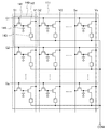
図7に示すように、画素部111は、信号線S1〜信号線Sx、走査線G1〜走査線Gy、電源線V1〜電源線Vxを有している。そして、画素140は、信号線S1〜信号線Sxのいずれか一つと、走査線G1〜走査線Gyのいずれか一つと、電源線V1〜電源線Vxのいずれか一つとを有する。
As illustrated in FIG. 7, the
そして、各画素140において、トランジスタ141は、そのゲート電極が走査線Gj(jは1乃至yのいずれか一つ)に接続されている。トランジスタ141は、その第1端子が、画像信号の与えられている信号線Si(iは1乃至xのいずれか一つ)に接続されており、その第2端子が、トランジスタ142のゲート電極に接続されている。トランジスタ142は、その第1端子が、電源電位の与えられている電源線Viに接続されており、その第2端子が、発光素子143の画素電極に接続される。発光素子143の共通電極には、共通電位COMが与えられる。
In each pixel 140, the gate electrode of the
また、図7では、画素140が保持容量144を有する場合を例示している。保持容量144は、トランジスタ142のゲート電極に接続されており、上記保持容量144によって、トランジスタ142のゲート電極の電位が保持される。具体的に、保持容量144が有する一対の電極は、一方がトランジスタ142のゲート電極に接続され、他方が固定電位の与えられているノード、例えば電源線Viなどに、接続されている。
FIG. 7 illustrates the case where the pixel 140 includes the
なお、図7では、トランジスタ141、トランジスタ142がnチャネル型である場合を例示しているが、これらのトランジスタはnチャネル型とpチャネル型のどちらでも良い。
Note that FIG. 7 illustrates the case where the
また、画素140は、必要に応じて、トランジスタ、ダイオード、抵抗素子、保持容量、インダクタなどのその他の回路素子を、さらに有していても良い。 The pixel 140 may further include other circuit elements such as a transistor, a diode, a resistance element, a storage capacitor, and an inductor as necessary.
なお、トランジスタ141は、活性層の片側にだけ存在するゲート電極を少なくとも有していれば良いが、活性層を間に挟んで存在する一対のゲート電極を有していても良い。トランジスタ141が、活性層を間に挟んで存在する一対のゲート電極を有している場合、一方のゲート電極には信号線が接続され、他方のゲート電極(バックゲート電極)は、電気的に絶縁しているフローティングの状態であっても良いし、電位が他から与えられている状態であっても良い。後者の場合、一対の電極に、同じ高さの電位が与えられていても良いし、バックゲート電極にのみ接地電位などの固定の電位が与えられていても良い。バックゲート電極に与える電位の高さを制御することで、トランジスタ141の閾値電圧を制御することができる。
Note that the
また、トランジスタ141は、単数のゲート電極と単数のチャネル形成領域を有するシングルゲート構造であっても良いし、電気的に接続された複数のゲート電極を有することで、チャネル形成領域を複数有する、マルチゲート構造であっても良い。
The
次に、図7に示した画素部111の動作について説明する。
Next, an operation of the
まず、書き込み期間において、走査線G1〜走査線Gyが順に選択される。例えば走査線Gjが選択されると、走査線Gjにゲート電極が接続されているトランジスタ141がオンになる。そして、信号線S1〜信号線Sxに入力された画像信号の電位が、トランジスタ141がオンになることで、トランジスタ142のゲート電極に与えられる。走査線Gjの選択が終了すると、トランジスタ141がオフになり、画像信号の電位はトランジスタ142のゲート電極において保持される。
First, in the writing period, the scanning lines G1 to Gy are sequentially selected. For example, when the scanning line Gj is selected, the
なお、書き込み期間では、発光素子143の共通電極に、共通電位COMが与えられている。そして、画像信号の電位に従って発光素子143の発光状態が定まる。具体的には、画像信号の電位に従ってトランジスタ142がオンになっている場合、発光素子143に電流が供給されることで発光素子143が点灯する。発光素子143に流れる電流の値は、トランジスタ142のドレイン電流によってほぼ決まる。よって、発光素子143は、画像信号の電位に従ってその輝度が定まる。逆に、画像信号の電位に従って、トランジスタ142がオフになっている場合、発光素子143への電流の供給は行われず、発光素子143は消灯する。
Note that in the writing period, the common potential COM is applied to the common electrode of the light-emitting
次いで、書き込み期間が終了し保持期間が開始されると、トランジスタ141がオフになる。そして、書き込み期間においてトランジスタ142のゲート電極に与えられた画像信号の電位は、保持容量144により保持される。よって、発光素子143は、書き込み期間で定められた発光状態を維持する。
Next, when the writing period ends and the holding period starts, the
上記動作により、画素部111に画像を表示することができる。
With the above operation, an image can be displayed on the
次いで、画素140の具体的な構成の一例について説明する。図8に、画素140の上面図の一例を示す。なお、図8では、画素140のレイアウトを明確に示すために、各種の絶縁膜を省略して、画素140の上面図を示す。また、図8では、画素140のレイアウトを明確に示すために、画素電極上の電界発光層と共通電極を省略して、画素140の上面図を示す。 Next, an example of a specific configuration of the pixel 140 will be described. FIG. 8 shows an example of a top view of the pixel 140. In FIG. 8, in order to clearly show the layout of the pixel 140, various insulating films are omitted, and a top view of the pixel 140 is shown. Further, in FIG. 8, in order to clearly show the layout of the pixel 140, an electroluminescent layer on the pixel electrode and a common electrode are omitted, and a top view of the pixel 140 is shown.
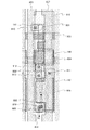
図8では、トランジスタ141の活性層として機能する半導体膜801と、トランジスタ142の活性層として機能する半導体膜802とが、絶縁表面を有する基板上に設けられている。半導体膜801は、保持容量144の電極の一つとしても機能する。
In FIG. 8, a
そして、半導体膜801上には、ゲート絶縁膜を間に挟んで、トランジスタ141のゲート電極、及び走査線として機能する導電膜803が設けられている。また、半導体膜801上には、ゲート絶縁膜を間に挟んで、保持容量144の電極の一つとして機能する導電膜804が設けられている。半導体膜801と導電膜804とがゲート絶縁膜を間に挟んで重なっている部分が、保持容量144に相当する。また、半導体膜802上には、ゲート絶縁膜を間に挟んで、トランジスタ142のゲート電極として機能する導電膜805が設けられている。
Over the
導電膜803、導電膜804、及び導電膜805上には第1層間絶縁膜が形成されている。上記第1層間絶縁膜上には、信号線として機能する導電膜806と、電源線として機能する導電膜807と、導電膜808と、導電膜809が設けられている。
A first interlayer insulating film is formed over the
導電膜806は、第1層間絶縁膜及びゲート絶縁膜に形成された開口部810を介して、半導体膜801に接続されている。導電膜807は、第1層間絶縁膜及びゲート絶縁膜に形成された開口部811を介して、半導体膜802に接続されている。導電膜808は、第1層間絶縁膜及びゲート絶縁膜に形成された開口部812を介して、半導体膜802に接続され、なおかつ、第1層間絶縁膜に形成された開口部813を介して、導電膜805に接続されている。導電膜809は、第1層間絶縁膜及びゲート絶縁膜に形成された開口部814を介して、半導体膜802に接続されている。
The
導電膜806、導電膜807、導電膜808、及び導電膜809上には、第2層間絶縁膜が形成されている。第2層間絶縁膜上には、画素電極として機能する導電膜815が設けられている。導電膜815は、第2層間絶縁膜に形成された開口部816を介して、導電膜809に接続されている。
A second interlayer insulating film is formed over the
なお、本発明の一態様に係る表示装置では、図1に示した画素部111において、白色などの単色の光を発する発光素子と、カラーフィルタを組み合わせることで、フルカラー画像の表示を行う、カラーフィルタ方式を採用することができる。或いは、互いに異なる色相の光を発する複数の発光素子を用いて、フルカラー画像の表示を行う方式を採用することもできる。この方式は、発光素子が有する一対の電極間に設けられる電界発光層を、対応する色ごとに塗り分けるため、塗り分け方式と呼ばれる。
Note that in the display device according to one embodiment of the present invention, in the
塗り分け方式の場合、電界発光層の塗り分けは、通常、メタルマスクなどのマスクを用いて、蒸着法で行われる。そのため、画素のサイズは蒸着法による電界発光層の塗り分け精度に依存する。一方、カラーフィルタ方式の場合、塗り分け方式とは異なり、電界発光層の塗り分けを行う必要がない。よって、塗り分け方式の場合よりも、画素サイズの縮小化が容易であり、高精細の画素部を実現することができる。そして、画素部が高精細であることは、画像の立体感や奥行き感を高める上で有利である。よって、カラーフィルタ方式の発光装置は、立体感や奥行き感を高める上で、本発明の一態様に係る表示装置に、より適していると言える。 In the case of the separate coating method, the separate application of the electroluminescent layer is usually performed by vapor deposition using a mask such as a metal mask. Therefore, the size of the pixel depends on the coating accuracy of the electroluminescent layer by vapor deposition. On the other hand, in the case of the color filter method, unlike the separate coating method, it is not necessary to separate the electroluminescent layer. Therefore, it is easier to reduce the pixel size than in the case of the separate coloring method, and a high-definition pixel portion can be realized. The high definition of the pixel portion is advantageous in enhancing the stereoscopic effect and depth feeling of the image. Therefore, it can be said that the color filter light-emitting device is more suitable for the display device according to one embodiment of the present invention, in terms of enhancing stereoscopic effect and depth.
また、発光装置には、トランジスタが形成された基板(素子基板)側から発光素子の光を取り出すボトムエミッション構造と、素子基板とは反対の側から発光素子の光を取り出すトップエミッション構造とがある。トップエミッション構造の場合、発光素子から発せられる光を、配線、トランジスタ、保持容量などの各種素子によって遮られることがないため、ボトムエミッション構造に比べて、画素からの光の取り出し効率を高めることができる。よって、トップエミッション構造は、発光素子に供給する電流値を低く抑えても、高い輝度を得ることができるため、発光素子の長寿命化に有利である。 In addition, the light emitting device includes a bottom emission structure in which light of the light emitting element is extracted from the substrate (element substrate) side where the transistor is formed, and a top emission structure in which light of the light emitting element is extracted from the side opposite to the element substrate. . In the case of the top emission structure, light emitted from the light emitting element is not blocked by various elements such as wirings, transistors, and storage capacitors, so that the light extraction efficiency from the pixel can be improved compared to the bottom emission structure. it can. Therefore, the top emission structure is advantageous in extending the life of the light-emitting element because high luminance can be obtained even when the current value supplied to the light-emitting element is kept low.
また、本発明の一態様に係る表示装置では、電界発光層から発せられる光を発光素子内で共振させる、マイクロキャビティ(微小光共振器)構造を有していても良い。マイクロキャビティ構造により、特定の波長の光について、発光素子からの取り出し効率を高めることができるので、画素部の輝度と色純度を向上させることができる。 Further, the display device according to one embodiment of the present invention may have a microcavity (micro optical resonator) structure in which light emitted from the electroluminescent layer is resonated in the light emitting element. With the microcavity structure, the light extraction efficiency of the light having a specific wavelength can be increased, so that the luminance and color purity of the pixel portion can be improved.
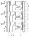
図9に、マイクロキャビティ構造を有する画素の断面図を、一例として示す。なお、図9では、赤に対応する画素の断面の一部、青に対応する画素の断面の一部と、緑に対応する画素の断面の一部とを示している。そして、上記3つの画素における断面の一部は、図8に示す画素140の上面図の、破線A1−A2に対応しているものとする。 FIG. 9 shows a cross-sectional view of a pixel having a microcavity structure as an example. FIG. 9 shows a part of a cross section of a pixel corresponding to red, a part of a cross section of a pixel corresponding to blue, and a part of a cross section of a pixel corresponding to green. A part of a cross section of the three pixels corresponds to a broken line A1-A2 in the top view of the pixel 140 illustrated in FIG.
具体的に、図9では、赤に対応した画素140rと、緑に対応した画素140gと、青に対応した画素140bとが示されている。画素140r、画素140g、画素140bは、それぞれ画素電極815r、画素電極815g、画素電極815bを有する。上記画素電極815r、画素電極815g、画素電極815bは、画素140r、画素140g、画素140bのそれぞれにおいて、基板840上のトランジスタ142と、導電膜809を介して接続されている。
Specifically, FIG. 9 shows a
そして、画素電極815r、画素電極815g、及び画素電極815b上には絶縁膜を有する隔壁830が設けられている。隔壁830は開口部を有し、上記開口部において、画素電極815r、画素電極815g、及び画素電極815bが、それぞれ一部露出している。また、上記露出している領域を覆うように、隔壁830上に、電界発光層831と、可視光に対して透光性を有する共通電極832とが、順に積層されている。
A
画素電極815rと、電界発光層831と、共通電極832とが重なる部分が、赤に対応した発光素子841rに相当する。画素電極815gと、電界発光層831と、共通電極832とが重なる部分が、緑に対応した発光素子841gに相当する。画素電極815bと、電界発光層831と、共通電極832とが重なる部分が、青に対応した発光素子841bに相当する。
A portion where the
また、基板842は、発光素子841r、発光素子841g、及び発光素子841bを間に挟むように、基板840と対峙している。基板842上には、画素140rに対応した着色層843r、画素140gに対応した着色層843g、画素140bに対応した着色層843bが設けられている。着色層843rは、赤に対応した波長領域の光の透過率が、他の波長領域の光の透過率より高い層であり、着色層843gは、緑に対応した波長領域の光の透過率が、他の波長領域の光の透過率より高い層であり、着色層843bは、青に対応した波長領域の光の透過率が、他の波長領域の光の透過率より高い層である。
The
さらに、基板842上には、着色層843r、着色層843g、着色層843bを覆うように、オーバーコート844が設けられている。オーバーコート844は、着色層843r、着色層843g、着色層843bを保護するための、可視光に対して透光性を有する層であり、平坦性の高い樹脂材料を用いるのが好ましい。着色層843r、着色層843g、及び着色層843bと、オーバーコート844とを合わせてカラーフィルタと見なしても良いし、着色層843r、着色層843g、及び着色層843bのそれぞれをカラーフィルタと見なしても良い。
Further, an
そして、図9に示すように、本発明の一態様では、画素電極815rに、可視光の反射率が高い導電膜845rと、可視光の透過率が上記導電膜よりも高い導電膜846rとを、順に積層して用いる。また、画素電極815gに、可視光の反射率が高い導電膜845gと、可視光の透過率が上記導電膜よりも高い導電膜846gとを、順に積層して用いる。導電膜846gの膜厚は、導電膜846rの膜厚よりも小さいものとする。また、画素電極815bに、可視光の反射率が高い導電膜845bを用いる。
As shown in FIG. 9, in one embodiment of the present invention, the
よって、図9に示す発光装置では、発光素子841rにおいて、電界発光層831から発せられた光の光路長は、導電膜845rと共通電極832の距離により定まる。また、発光素子841gにおいて、電界発光層831から発せられた光の光路長は、導電膜845gと共通電極832の距離により定まる。また、発光素子841bにおいて、電界発光層831から発せられた光の光路長は、導電膜845bと共通電極832の距離により定まる。
Therefore, in the light-emitting device illustrated in FIG. 9, in the light-emitting
本発明の一態様では、発光素子841rと、発光素子841gと、発光素子841bにそれぞれ対応する光の波長に合わせて、上記光路長を調整することで、電界発光層831から発せられた光を上記各発光素子内において共振させる、マイクロキャビティ構造とする。例えば、図9の場合、導電膜845r、導電膜845g、または導電膜845bと、共通電極832との間の距離をL、電界発光層831の屈折率をn、共振させたい光の波長をλとすると、距離Lと屈折率nの積が、波長λの(2N−1)/4倍(Nは自然数)になるようにすると良い。
In one embodiment of the present invention, light emitted from the
本発明の一態様では、上記マイクロキャビティ構造を採用することで、発光素子841rから発せられる光において、赤に対応した波長を有する光の強度が、共振により高まる。よって、着色層843rを通して得られる赤の光の色純度及び輝度が高まる。また、本発明の一態様では、上記マイクロキャビティ構造を採用することで、発光素子841gから発せられる光において、緑に対応した波長を有する光の強度が、共振により高まる。よって、着色層843gを通して得られる緑の光の色純度及び輝度が高まる。また、本発明の一態様では、上記マイクロキャビティ構造を採用することで、発光素子841bから発せられる光において、青に対応した波長を有する光の強度が、共振により高まる。よって、着色層843bを通して得られる青の光の色純度及び輝度が高まる。
In one embodiment of the present invention, by using the microcavity structure, the intensity of light having a wavelength corresponding to red in light emitted from the light-emitting
なお、図9では、赤、緑、青の3色に対応する画素を用いる構成について示したが、本発明の一態様では、当該構成に限定されない。本発明の一態様で用いる色の組み合わせは、例えば、赤、緑、青、黄の4色、または、シアン、マゼンタ、イエローの3色を用いていても良い。或いは、上記色の組み合わせは、淡色の赤、緑、及び青、並びに濃色の赤、緑、及び青の6色を用いていても良い。或いは、上記色の組み合わせは、赤、緑、青、シアン、マゼンタ、イエローの6色を用いていても良い。 Note that FIG. 9 illustrates a structure in which pixels corresponding to three colors of red, green, and blue are used; however, one embodiment of the present invention is not limited to the structure. As the combination of colors used in one embodiment of the present invention, for example, four colors of red, green, blue, and yellow, or three colors of cyan, magenta, and yellow may be used. Alternatively, the combination of the colors may use six colors of light red, green, and blue and dark red, green, and blue. Alternatively, six colors of red, green, blue, cyan, magenta, and yellow may be used as the color combination.
なお、例えば、赤、緑、及び青の画素を用いて表現できる色は、色度図上のそれぞれの発光色に対応する3点が描く三角形の内側に示される色に限られる。従って、赤、緑、青、黄の画素を用いた場合のように、色度図上の該三角形の外側に発光色が存在する光源を別途加えることで、当該発光装置において表現できる色域を拡大し、色再現性を豊かにすることができる。 Note that, for example, colors that can be expressed using red, green, and blue pixels are limited to colors that are shown inside a triangle drawn by three points corresponding to the respective emission colors on the chromaticity diagram. Therefore, as in the case of using red, green, blue, and yellow pixels, a color gamut that can be expressed in the light emitting device can be obtained by separately adding a light source having a light emitting color outside the triangle on the chromaticity diagram. Enlarge and enhance color reproducibility.
また、図9では、発光素子841r、発光素子841g、発光素子841bのうち、光の波長λが最も短い発光素子841bにおいて、可視光の反射率が高い導電膜845bを画素電極として用い、他の発光素子841r、発光素子841gにおいては、膜厚が互いに異なる導電膜846r及び導電膜846gを用いることにより、光路長を調整している。本発明の一態様では、波長λが最も短い発光素子841bにおいても、可視光の反射率が高い導電膜845b上に、導電膜846r及び導電膜846gのような、可視光の透過率の高い導電膜を設けていても良い。ただし、図9に示すように、波長λが最も短い発光素子841bにおいて、可視光の反射率が高い導電膜845bで画素電極を構成する場合、全ての発光素子において、画素電極に可視光の透過率が高い導電膜を用いる場合よりも、画素電極の作製工程が簡素化されるため、好ましい。
In FIG. 9, among the
なお、可視光の反射率が高い導電膜845bは、可視光の透過率が高い導電膜846r及び導電膜846gに比べて、仕事関数が小さい場合が多い。よって、光の波長λが最も短い発光素子841bでは、発光素子841r、発光素子841gに比べて、陽極である画素電極815bから電界発光層831への正孔注入が行われにくいため、発光効率が低い傾向にある。そこで、本発明の一態様では、光の波長λが最も短い発光素子841bにおいて、電界発光層831のうち、可視光の反射率が高い導電膜845bと接する層において、正孔輸送性の高い物質に、当該正孔輸送性の高い物質に対してアクセプター性(電子受容性)を示す物質を含有させた複合材料を用いることが好ましい。上記複合材料を、陽極である画素電極815bに接して形成することにより、画素電極815bから電界発光層831への正孔注入が行われやすくなり、発光素子841bの発光効率を高めることができる。
Note that the
アクセプター性を示す物質としては、7,7,8,8−テトラシアノ−2,3,5,6−テトラフルオロキノジメタン(略称:F4−TCNQ)、クロラニル等を挙げることができる。また、遷移金属酸化物を挙げることができる。また、元素周期表における第4族乃至第8族に属する金属の酸化物を挙げることができる。具体的には、酸化バナジウム、酸化ニオブ、酸化タンタル、酸化クロム、酸化モリブデン、酸化タングステン、酸化マンガン、酸化レニウムはアクセプター性が高いため好ましい。中でも特に、酸化モリブデンは大気中でも安定であり、吸湿性が低く、扱いやすいため好ましい。 As a substance exhibiting acceptor properties, 7,7,8,8-tetracyano-2,3,5,6-tetrafluoroquinodimethane (abbreviation: F 4 -TCNQ), chloranil, and the like can be given. Moreover, a transition metal oxide can be mentioned. In addition, oxides of metals belonging to Groups 4 to 8 in the periodic table can be given. Specifically, vanadium oxide, niobium oxide, tantalum oxide, chromium oxide, molybdenum oxide, tungsten oxide, manganese oxide, and rhenium oxide are preferable because of their high acceptor properties. Among these, molybdenum oxide is especially preferable because it is stable in the air, has a low hygroscopic property, and is easy to handle.
複合材料に用いる正孔輸送性の高い物質としては、芳香族アミン化合物、カルバゾール誘導体、芳香族炭化水素、高分子化合物(オリゴマー、デンドリマー、ポリマー等)など、種々の化合物を用いることができる。なお、複合材料に用いる有機化合物としては、正孔輸送性の高い有機化合物であることが好ましい。具体的には、10−6cm2/Vs以上の正孔移動度を有する物質であることが好ましい。但し、電子よりも正孔の輸送性の高い物質であれば、これら以外のものを用いてもよい。 As the substance having a high hole-transport property used for the composite material, various compounds such as an aromatic amine compound, a carbazole derivative, an aromatic hydrocarbon, and a high molecular compound (oligomer, dendrimer, polymer, and the like) can be used. Note that the organic compound used for the composite material is preferably an organic compound having a high hole-transport property. Specifically, a substance having a hole mobility of 10 −6 cm 2 / Vs or higher is preferable. Note that other than these substances, any substance that has a property of transporting more holes than electrons may be used.
また、可視光の反射率が高い導電膜845r、導電膜845g、導電膜845bとしては、例えば、アルミニウム、銀、または、これらの金属材料を含む合金等を、単層で、或いは積層することで、形成することができる。また、導電膜845r、導電膜845g、導電膜845bを、可視光の反射率の高い導電膜と、膜厚の薄い導電膜(好ましくは20nm以下、更に好ましくは10nm以下)とを積層させて、形成してもよい。例えば、可視光の反射率の高い導電膜上に、薄いチタン膜やモリブデン膜を積層して、導電膜845bを形成することにより、可視光の反射率の高い導電膜(アルミニウム、アルミニウムを含む合金、または銀など)の表面に酸化膜が形成されるのを防ぐことができる。
As the
また、可視光の透過率が高い導電膜846r及び導電膜846gには、例えば、酸化インジウム、酸化スズ、酸化亜鉛、インジウム錫酸化物、インジウム亜鉛酸化物などを用いることができる。
For the
また、共通電極832は、例えば、光を透過する程度の薄い導電膜(好ましくは20nm以下、更に好ましくは10nm以下)と、導電性の金属酸化物で構成された導電膜とを積層することで、形成することができる。光を透過する程度の薄い導電膜は、銀、マグネシウム、またはこれらの金属材料を含む合金等を、単層で、或いは積層して形成することができる。導電性の金属酸化物としては、酸化インジウム、酸化スズ、酸化亜鉛、インジウム錫酸化物、インジウム亜鉛酸化物、またはこれらの金属酸化物材料に酸化シリコンを含ませたものを用いることができる。
For example, the
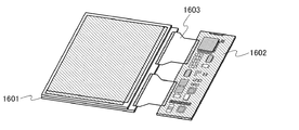
図10は、本発明の一態様に係る表示装置の、斜視図の一例である。図10では、発光装置を表示部に用いた場合の、表示装置を例示している。 FIG. 10 is an example of a perspective view of a display device according to one embodiment of the present invention. FIG. 10 illustrates a display device in the case where the light emitting device is used for the display portion.
図10に示す表示装置は、表示部1601と、回路基板1602と、接続部1603とを有している。
The display device illustrated in FIG. 10 includes a
回路基板1602には、画像処理部が設けられており、接続部1603を介して各種信号や電源電位が表示部1601に入力される。接続部1603には、FPC(Flexible Printed Circuit)などを用いることができる。また、接続部1603にCOFテープを用いる場合、画像処理部の一部の回路、或いは表示部1601が有する駆動回路の一部などを別途用意したチップに形成しておき、COF(Chip On Film)法を用いて当該チップをCOFテープに接続しておいても良い。
The
本実施の形態は、上記実施の形態と組み合わせて実施することが可能である。 This embodiment can be implemented in combination with the above embodiment.
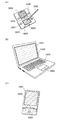
本発明の一態様に係る表示装置は、立体感、奥行き感の高い画像の表示を行うことができる。本発明の一態様に係る表示装置は、画像表示装置、ノート型パーソナルコンピュータ、記録媒体を備えた画像再生装置(代表的にはDVD:Digital Versatile Disc等の記録媒体を再生し、その画像を表示しうるディスプレイを有する装置)に用いることができる。その他に、本発明の一態様に係る表示装置を用いることができる電子機器として、携帯電話、携帯型ゲーム機、携帯情報端末、電子書籍、ビデオカメラ、デジタルスチルカメラ、ゴーグル型ディスプレイ(ヘッドマウントディスプレイ)、ナビゲーションシステム、音響再生装置(カーオーディオ、デジタルオーディオプレイヤー等)、複写機、ファクシミリ、プリンター、プリンター複合機、現金自動預け入れ払い機(ATM)、自動販売機などが挙げられる。これら電子機器の具体例を図11に示す。 The display device according to one embodiment of the present invention can display an image with a high sense of depth and depth. A display device according to one embodiment of the present invention includes an image display device, a notebook personal computer, and an image reproduction device including a recording medium (typically, a recording medium such as a DVD: Digital Versatile Disc) is reproduced and the image is displayed. A device having a display capable of being used). In addition, as an electronic device in which the display device according to one embodiment of the present invention can be used, a mobile phone, a portable game machine, a portable information terminal, an electronic book, a video camera, a digital still camera, a goggle type display (head mounted display) ), Navigation systems, sound reproducing devices (car audio, digital audio player, etc.), copying machines, facsimiles, printers, printer multifunction devices, automatic teller machines (ATMs), vending machines, and the like. Specific examples of these electronic devices are shown in FIGS.
図11(A)は携帯型ゲーム機であり、筐体5001、筐体5002、画像表示部5003、画像表示部5004、マイクロホン5005、スピーカー5006、操作キー5007、スタイラス5008等を有する。本発明の一態様に係る表示装置は、画像表示部5003または画像表示部5004に用いることができる。画像表示部5003または画像表示部5004に本発明の一態様に係る表示装置を用いることで、立体感、奥行き感の高い画像の表示を行う携帯型ゲーム機を提供することができる。なお、図11(A)に示した携帯型ゲーム機は、2つの画像表示部5003と画像表示部5004とを有しているが、携帯型ゲーム機が有する画像表示部の数は、これに限定されない。
FIG. 11A illustrates a portable game machine, which includes a
図11(B)はノート型パーソナルコンピュータであり、筐体5201、画像表示部5202、キーボード5203、ポインティングデバイス5204等を有する。本発明の一態様に係る表示装置は、画像表示部5202に用いることができる。画像表示部5202に本発明の一態様に係る表示装置を用いることで、立体感、奥行き感の高い画像の表示を行うノート型パーソナルコンピュータを提供することができる。
FIG. 11B illustrates a laptop personal computer, which includes a
図11(C)は携帯情報端末であり、筐体5401、画像表示部5402、操作キー5403等を有する。本発明の一態様に係る表示装置は、画像表示部5402に用いることができる。画像表示部5402に本発明の一態様に係る表示装置を用いることで、立体感、奥行き感の高い画像の表示を行う携帯情報端末を提供することができる。
FIG. 11C illustrates a portable information terminal, which includes a
以上の様に、本発明の適用範囲は極めて広く、あらゆる分野の電子機器に用いることが可能である。 As described above, the applicable range of the present invention is so wide that it can be used for electronic devices in various fields.
本実施例は、上記実施の形態と適宜組み合わせて実施することができる。 This example can be implemented in combination with any of the above embodiments as appropriate.
100 表示装置
101 画像処理部
102 表示部
103 画像データ
104 制御装置
105 演算装置
106 入力部
107 緩衝記憶装置
108 不揮発性記憶装置
109 表示部用コントローラ
110 データベース
111 画素部
112 駆動回路
130 特徴点
131 消失点
132 中心点
133 中心点
134 破線
135 破線
136 中心点
137 中心点
140 画素
140b 画素
140g 画素
140r 画素
141 トランジスタ
142 トランジスタ
143 発光素子
144 保持容量
801 半導体膜
802 半導体膜
803 導電膜
804 導電膜
805 導電膜
806 導電膜
807 導電膜
808 導電膜
809 導電膜
810 開口部
811 開口部
812 開口部
813 開口部
814 開口部
815 導電膜
816 開口部
815b 画素電極
815g 画素電極
815r 画素電極
830 隔壁
831 電界発光層
832 共通電極
840 基板
841b 発光素子
841g 発光素子
841r 発光素子
842 基板
843b 着色層
843g 着色層
843r 着色層
844 オーバーコート
845b 導電膜
845g 導電膜
845r 導電膜
846g 導電膜
846r 導電膜
1601 表示部
1602 回路基板
1603 接続部
5001 筐体
5002 筐体
5003 画像表示部
5004 画像表示部
5005 マイクロホン
5006 スピーカー
5007 操作キー
5008 スタイラス
5201 筐体
5202 画像表示部
5203 キーボード
5204 ポインティングデバイス
5401 筐体
5402 画像表示部
5403 操作キー
DESCRIPTION OF SYMBOLS 100
Claims (7)
前記複数の対象物の画像データから特徴量をそれぞれ取得し、
前記特徴量と、データベース中に蓄積されている、モデルとなる対象物の特徴量に関連づけられた、当該モデルとなる対象物の大きさのデータとから、前記複数の対象物の大きさのデータを得て、
前記第1の画像中における前記複数の対象物どうしの相対的な大きさと、前記複数の対象物の大きさのデータとから、前記複数の対象物どうしの前後関係を定め、
前記前後関係に従って、前記複数の対象物のうち、前に位置する対象物ほど大きく、なおかつ、輪郭が強調されるように、前記複数の対象物の画像データに画像処理を施し、
前記画像処理を施した前記複数の対象物の画像データと、前記背景の画像データとを合成することで、第2の画像に対応した第2の画像データを形成する画像処理方法。 Separating the first image data corresponding to the first image into a plurality of object image data and a background image data;
Obtaining feature quantities from the image data of the plurality of objects,
The data of the size of the plurality of objects is obtained from the feature quantity and the data of the size of the object to be the model that is stored in the database and is associated with the feature quantity of the object to be the model. Get
From the relative size of the plurality of objects in the first image and the data of the size of the plurality of objects, a front-rear relationship between the plurality of objects is determined,
In accordance with the front-rear relationship, among the plurality of objects, the object positioned in front is larger, and image processing is performed on the image data of the plurality of objects so that the contour is emphasized,
An image processing method for forming second image data corresponding to a second image by combining the image data of the plurality of objects subjected to the image processing and the background image data.
前記複数の対象物の画像データから特徴量をそれぞれ取得し、
前記特徴量と、データベース中に蓄積されている、モデルとなる対象物の特徴量に関連づけられた、当該モデルとなる対象物の大きさのデータとから、前記複数の対象物の大きさのデータを得て、
前記第1の画像中における前記複数の対象物どうしの相対的な大きさと、前記複数の対象物の大きさのデータとから、前記複数の対象物と、観察者の視点との間の相対的な距離を定め、
前記複数の対象物のうち、前に位置する対象物ほど、前記距離により定められた拡大率に従って大きく、なおかつ、前記距離により定められた度合いに従って輪郭が強調されるように、前記複数の対象物の画像データに画像処理を施し、
前記画像処理を施した前記複数の対象物の画像データと、前記背景の画像データとを合成することで、第2の画像に対応した第2の画像データを形成する画像処理方法。 Separating the first image data corresponding to the first image into a plurality of object image data and a background image data;
Obtaining feature quantities from the image data of the plurality of objects,
The data of the size of the plurality of objects is obtained from the feature quantity and the data of the size of the object to be the model that is stored in the database and is associated with the feature quantity of the object to be the model. Get
Based on the relative size of the plurality of objects in the first image and the data of the size of the plurality of objects, the relative between the plurality of objects and the viewpoint of the observer Set a certain distance,
Among the plurality of objects, the plurality of objects are arranged such that a front object is larger in accordance with an enlargement ratio determined by the distance and an outline is emphasized in accordance with a degree determined by the distance. Image processing of the image data,
An image processing method for forming second image data corresponding to a second image by combining the image data of the plurality of objects subjected to the image processing and the background image data.
前記第1の画像における、一の消失点と、前記複数の対象物がそれぞれ有する第1の中心点との間の距離をL1とし、
前記第2の画像における、前記一の消失点と、前記複数の対象物がそれぞれ有する第2の中心点との間の距離をL2とすると、
前記複数の対象物のうち、前に位置する対象物ほど、前記L2から前記L1を差し引くことで得られる距離の差が大きい画像処理方法。 In claim 1 or claim 2,
In the first image, the distance between one vanishing point and the first center point of each of the plurality of objects is L1,
In the second image, when the distance between the one vanishing point and the second center point of each of the plurality of objects is L2,
The image processing method in which the difference in distance obtained by subtracting the L1 from the L2 is larger for the object located in front of the plurality of objects.
前記第1の中心点は、前記第1の画像における前記複数の対象物がそれぞれ有する重心点であり、
前記第2の中心点は、前記第2の画像における前記複数の対象物がそれぞれ有する重心点である画像処理方法。 In claim 3,
The first center point is a centroid point that each of the plurality of objects in the first image has,
The image processing method, wherein the second center point is a center-of-gravity point that each of the plurality of objects in the second image has.
上記画像信号に従って前記第2の画像の表示を行う表示部と、を有し、
前記表示部は、画素部と、前記画素部の駆動を制御する駆動回路とを有し、
前記画素部が有する複数の画素は、発光素子と、前記発光素子への電流の供給を制御する第1トランジスタと、前記第1トランジスタが有するゲート電極への、前記画像信号の電位の供給を制御する第2トランジスタと、特定の波長領域の光の透過率が他の波長領域の光の透過率よりも高い着色層とを、それぞれ有し、
前記発光素子は、画素電極と、可視光に対して透光性を有する共通電極と、前記画素電極と前記共通電極の間に位置する電界発光層とを有し、
前記複数の画素のうち、第1の画素が有する前記発光素子は、前記画素電極が、可視光を反射する第1の導電膜で構成されており、
前記複数の画素のうち、第2の画素が有する前記発光素子は、前記第1の導電膜と、前記第1の導電膜上に位置し、なおかつ可視光に対して透光性を有する第2の導電膜とで前記画素電極が構成されており、
前記複数の画素のうち、第3の画素が有する前記発光素子は、第1の導電膜と、前記第1の導電膜上に位置し、なおかつ可視光に対して透光性を有する第3の導電膜とで前記画素電極が構成されており、
前記第2の導電膜の膜厚は、前記第3の導電膜よりも小さい表示装置。 5. The image processing method according to claim 1, wherein the second image data is generated from the first image data, and an image signal is generated using the second image data. An image processing unit for generating
A display unit for displaying the second image according to the image signal,
The display unit includes a pixel unit and a drive circuit that controls driving of the pixel unit,
The plurality of pixels included in the pixel portion controls the supply of the potential of the image signal to a light emitting element, a first transistor that controls supply of current to the light emitting element, and a gate electrode included in the first transistor. Each having a second transistor, and a colored layer in which the transmittance of light in a specific wavelength region is higher than the transmittance of light in other wavelength regions,
The light-emitting element includes a pixel electrode, a common electrode having a light-transmitting property with respect to visible light, and an electroluminescent layer positioned between the pixel electrode and the common electrode.
Among the plurality of pixels, the light emitting element of the first pixel has the pixel electrode made of a first conductive film that reflects visible light,
The light emitting element included in the second pixel among the plurality of pixels is located on the first conductive film and the first conductive film, and has a second property of transmitting visible light. The pixel electrode is composed of the conductive film of
The light-emitting element of the third pixel among the plurality of pixels is a first conductive film and a third light-transmitting element that is located on the first conductive film and has a light-transmitting property with respect to visible light. The pixel electrode is composed of a conductive film,
A display device in which the film thickness of the second conductive film is smaller than that of the third conductive film.
上記画像信号に従って前記第2の画像の表示を行う表示部と、を有し、
前記表示部は、画素部と、前記画素部の駆動を制御する駆動回路とを有し、
前記画素部が有する複数の画素は、発光素子と、前記発光素子への電流の供給を制御する第1トランジスタと、前記第1トランジスタが有するゲート電極への、前記画像信号の電位の供給を制御する第2トランジスタと、特定の波長領域の光の透過率が他の波長領域の光の透過率よりも高い着色層とを、それぞれ有し、
前記発光素子は、画素電極と、可視光に対して透光性を有する共通電極と、前記画素電極と前記共通電極の間に位置する電界発光層とを有し、
前記複数の画素のうち、第1の画素が有する前記発光素子は、前記画素電極が、可視光を反射する第1の導電膜で構成されており、
前記複数の画素のうち、第2の画素が有する前記発光素子は、前記第1の導電膜と、前記第1の導電膜上に位置し、なおかつ可視光に対して透光性を有する第2の導電膜とで前記画素電極が構成されており、
前記複数の画素のうち、第3の画素が有する前記発光素子は、第1の導電膜と、前記第1の導電膜上に位置し、なおかつ可視光に対して透光性を有する第3の導電膜とで前記画素電極が構成されており、
前記第2の導電膜の膜厚は、前記第3の導電膜よりも小さく、
前記電界発光層のうち、前記画素電極に接する領域には、正孔輸送性の高い物質に、当該正孔輸送性の高い物質に対してアクセプター性を示す物質を含有させた複合材料を用いる表示装置。 5. The image processing method according to claim 1, wherein the second image data is generated from the first image data, and an image signal is generated using the second image data. An image processing unit for generating
A display unit for displaying the second image according to the image signal,
The display unit includes a pixel unit and a drive circuit that controls driving of the pixel unit,
The plurality of pixels included in the pixel portion controls the supply of the potential of the image signal to a light emitting element, a first transistor that controls supply of current to the light emitting element, and a gate electrode included in the first transistor. Each having a second transistor, and a colored layer in which the transmittance of light in a specific wavelength region is higher than the transmittance of light in other wavelength regions,
The light-emitting element includes a pixel electrode, a common electrode having a light-transmitting property with respect to visible light, and an electroluminescent layer positioned between the pixel electrode and the common electrode.
Among the plurality of pixels, the light emitting element of the first pixel has the pixel electrode made of a first conductive film that reflects visible light,
The light emitting element included in the second pixel among the plurality of pixels is located on the first conductive film and the first conductive film, and has a second property of transmitting visible light. The pixel electrode is composed of the conductive film of
The light-emitting element of the third pixel among the plurality of pixels is a first conductive film and a third light-transmitting element that is located on the first conductive film and has a light-transmitting property with respect to visible light. The pixel electrode is composed of a conductive film,
The film thickness of the second conductive film is smaller than the third conductive film,
A display using a composite material in which a substance having a high hole-transport property and a substance having an acceptor property with respect to the substance having a high hole-transport property are included in a region in contact with the pixel electrode in the electroluminescent layer apparatus.
Priority Applications (1)
| Application Number | Priority Date | Filing Date | Title |
|---|---|---|---|
| JP2012062922A JP2012215852A (en) | 2011-03-25 | 2012-03-20 | Image processing method and display device |
Applications Claiming Priority (3)
| Application Number | Priority Date | Filing Date | Title |
|---|---|---|---|
| JP2011067069 | 2011-03-25 | ||
| JP2011067069 | 2011-03-25 | ||
| JP2012062922A JP2012215852A (en) | 2011-03-25 | 2012-03-20 | Image processing method and display device |
Related Child Applications (1)
| Application Number | Title | Priority Date | Filing Date |
|---|---|---|---|
| JP2016176359A Division JP6251789B2 (en) | 2011-03-25 | 2016-09-09 | Image processing method |
Publications (1)
| Publication Number | Publication Date |
|---|---|
| JP2012215852A true JP2012215852A (en) | 2012-11-08 |
Family
ID=46877410
Family Applications (2)
| Application Number | Title | Priority Date | Filing Date |
|---|---|---|---|
| JP2012062922A Withdrawn JP2012215852A (en) | 2011-03-25 | 2012-03-20 | Image processing method and display device |
| JP2016176359A Expired - Fee Related JP6251789B2 (en) | 2011-03-25 | 2016-09-09 | Image processing method |
Family Applications After (1)
| Application Number | Title | Priority Date | Filing Date |
|---|---|---|---|
| JP2016176359A Expired - Fee Related JP6251789B2 (en) | 2011-03-25 | 2016-09-09 | Image processing method |
Country Status (2)
| Country | Link |
|---|---|
| US (3) | US9313479B2 (en) |
| JP (2) | JP2012215852A (en) |
Families Citing this family (8)
| Publication number | Priority date | Publication date | Assignee | Title |
|---|---|---|---|---|
| US8849060B2 (en) | 2011-07-01 | 2014-09-30 | Semiconductor Energy Laboratory Co., Ltd. | Image processing method, image processing system and display device for modifying background colors based on object colors |
| US10021366B2 (en) * | 2014-05-02 | 2018-07-10 | Eys3D Microelectronics, Co. | Image process apparatus |
| KR101799381B1 (en) * | 2015-05-28 | 2017-11-22 | 삼성전자 주식회사 | Display apparatus and control method thereof |
| EP3099081B1 (en) | 2015-05-28 | 2020-04-29 | Samsung Electronics Co., Ltd. | Display apparatus and control method thereof |
| KR102423295B1 (en) | 2017-08-18 | 2022-07-21 | 삼성전자주식회사 | An apparatus for composing objects using depth map and a method thereof |
| CN109982064B (en) * | 2019-03-18 | 2021-04-27 | 影石创新科技股份有限公司 | Naked eye 3D virtual viewpoint image generation method and portable terminal |
| CN110046596B (en) * | 2019-04-23 | 2021-06-15 | 王雪燕 | Image modularization processing and multi-image module custom combination method, mobile terminal and readable storage medium |
| US12573006B2 (en) | 2022-11-01 | 2026-03-10 | Samsung Electronics Co., Ltd. | Display apparatus for obtaining output image using edge image and control method thereof |
Citations (8)
| Publication number | Priority date | Publication date | Assignee | Title |
|---|---|---|---|---|
| JPH0591545A (en) * | 1991-09-30 | 1993-04-09 | Toshiba Corp | Stereoscopic image recording/reproducing system |
| JP2006154169A (en) * | 2004-11-29 | 2006-06-15 | Seiko Epson Corp | Electro-optical element manufacturing method and electro-optical device |
| WO2006098188A1 (en) * | 2005-03-17 | 2006-09-21 | Idemitsu Kosan Co., Ltd. | Organic electroluminescent device |
| JP2007533076A (en) * | 2004-04-08 | 2007-11-15 | イーストマン コダック カンパニー | OLED with color change medium |
| JP2008503871A (en) * | 2004-06-16 | 2008-02-07 | イーストマン コダック カンパニー | Light emitting OLED microcavity pixel array |
| JP2008033897A (en) * | 2006-06-29 | 2008-02-14 | Matsushita Electric Ind Co Ltd | Image processing apparatus, image processing method, program, recording medium, and integrated circuit |
| JP2010206362A (en) * | 2009-03-02 | 2010-09-16 | Sharp Corp | Video processing apparatus, video processing method, and program for executing the same on computer |
| JP2011009729A (en) * | 2009-05-29 | 2011-01-13 | Semiconductor Energy Lab Co Ltd | Light-emitting element, light-emitting device, lighting device, and electronic appliance |
Family Cites Families (33)
| Publication number | Priority date | Publication date | Assignee | Title |
|---|---|---|---|---|
| JP2834318B2 (en) | 1990-11-28 | 1998-12-09 | 株式会社日立製作所 | 3D image processing method |
| US5732204A (en) | 1994-02-01 | 1998-03-24 | Ricoh Company, Ltd. | Method and device for 3D image processing |
| JP2919759B2 (en) | 1994-05-18 | 1999-07-19 | 三洋電機株式会社 | Optical filter and stereoscopic display device using the same |
| US5852673A (en) * | 1996-03-27 | 1998-12-22 | Chroma Graphics, Inc. | Method for general image manipulation and composition |
| JP2000209614A (en) * | 1999-01-14 | 2000-07-28 | Sony Corp | 3D image system |
| US6873723B1 (en) * | 1999-06-30 | 2005-03-29 | Intel Corporation | Segmenting three-dimensional video images using stereo |
| JP4570764B2 (en) * | 2000-12-01 | 2010-10-27 | 本田技研工業株式会社 | Motion information recognition system |
| US6741755B1 (en) * | 2000-12-22 | 2004-05-25 | Microsoft Corporation | System and method providing mixture-based determination of opacity |
| JP4017828B2 (en) | 2001-02-14 | 2007-12-05 | 富士フイルム株式会社 | Digital camera |
| JP4596219B2 (en) * | 2001-06-25 | 2010-12-08 | ソニー株式会社 | Image processing apparatus and method, recording medium, and program |
| US7103236B2 (en) | 2001-08-28 | 2006-09-05 | Adobe Systems Incorporated | Methods and apparatus for shifting perspective in a composite image |
| KR100516638B1 (en) * | 2001-09-26 | 2005-09-22 | 엘지전자 주식회사 | Video telecommunication system |
| DE10204500A1 (en) * | 2002-02-03 | 2003-08-14 | Fraunhofer Ges Forschung | Real-time detection and compensation method for lighting fluctuations in digital color image signals |
| JP2003259395A (en) | 2002-03-06 | 2003-09-12 | Matsushita Electric Ind Co Ltd | Stereoscopic display method and stereoscopic display device |
| US7263227B2 (en) * | 2002-04-25 | 2007-08-28 | Microsoft Corporation | Activity detector |
| US7120297B2 (en) * | 2002-04-25 | 2006-10-10 | Microsoft Corporation | Segmented layered image system |
| US7200266B2 (en) * | 2002-08-27 | 2007-04-03 | Princeton University | Method and apparatus for automated video activity analysis |
| US7343039B2 (en) * | 2003-06-13 | 2008-03-11 | Microsoft Corporation | System and process for generating representations of objects using a directional histogram model and matrix descriptor |
| US7627171B2 (en) * | 2003-07-03 | 2009-12-01 | Videoiq, Inc. | Methods and systems for detecting objects of interest in spatio-temporal signals |
| JP4285290B2 (en) * | 2004-03-22 | 2009-06-24 | 富士ゼロックス株式会社 | Image processing apparatus, image processing method, and program |
| EP1757087A4 (en) * | 2004-04-16 | 2009-08-19 | James A Aman | AUTOMATIC SYSTEM FOR FILMING VIDEO, FOLLOWING AN EVENT AND GENERATING CONTENT |
| JP4560711B2 (en) | 2004-06-22 | 2010-10-13 | 株式会社セガ | Image processing |
| US7664338B2 (en) | 2004-09-28 | 2010-02-16 | Qualcomm Incorporated | Perspective transformation of two-dimensional images |
| US8094928B2 (en) * | 2005-11-14 | 2012-01-10 | Microsoft Corporation | Stereo video for gaming |
| US7590344B2 (en) * | 2006-02-28 | 2009-09-15 | Microsoft Corp. | Adaptive processing for images captured with flash |
| IES20060564A2 (en) * | 2006-05-03 | 2006-11-01 | Fotonation Vision Ltd | Improved foreground / background separation |
| US8009903B2 (en) | 2006-06-29 | 2011-08-30 | Panasonic Corporation | Image processor, image processing method, storage medium, and integrated circuit that can adjust a degree of depth feeling of a displayed high-quality image |
| KR101388133B1 (en) * | 2007-02-16 | 2014-04-23 | 삼성전자주식회사 | Method and apparatus for creating a 3D model from 2D photograph image |
| US7808532B2 (en) * | 2007-05-29 | 2010-10-05 | Microsoft Corporation | Strategies for extracting foreground information using flash and no-flash image pairs |
| US8131098B2 (en) * | 2007-07-06 | 2012-03-06 | Panasonic Corporation | Image processing device, image processing method, image processing system, program, storage medium, and integrated circuit |
| US8086006B2 (en) * | 2007-09-21 | 2011-12-27 | Siemens Aktiengesellschaft | Method and system for evaluating image segmentation based on visibility |
| US8693759B2 (en) | 2008-11-13 | 2014-04-08 | Hitachi Medical Corporation | Image processing device and image processing method |
| US8406472B2 (en) * | 2010-03-16 | 2013-03-26 | Sony Corporation | Method and system for processing image data |
-
2012
- 2012-03-20 JP JP2012062922A patent/JP2012215852A/en not_active Withdrawn
- 2012-03-22 US US13/427,086 patent/US9313479B2/en not_active Expired - Fee Related
-
2016
- 2016-04-06 US US15/091,622 patent/US10051255B2/en not_active Expired - Fee Related
- 2016-09-09 JP JP2016176359A patent/JP6251789B2/en not_active Expired - Fee Related
-
2018
- 2018-06-18 US US16/010,600 patent/US10484660B2/en not_active Expired - Fee Related
Patent Citations (8)
| Publication number | Priority date | Publication date | Assignee | Title |
|---|---|---|---|---|
| JPH0591545A (en) * | 1991-09-30 | 1993-04-09 | Toshiba Corp | Stereoscopic image recording/reproducing system |
| JP2007533076A (en) * | 2004-04-08 | 2007-11-15 | イーストマン コダック カンパニー | OLED with color change medium |
| JP2008503871A (en) * | 2004-06-16 | 2008-02-07 | イーストマン コダック カンパニー | Light emitting OLED microcavity pixel array |
| JP2006154169A (en) * | 2004-11-29 | 2006-06-15 | Seiko Epson Corp | Electro-optical element manufacturing method and electro-optical device |
| WO2006098188A1 (en) * | 2005-03-17 | 2006-09-21 | Idemitsu Kosan Co., Ltd. | Organic electroluminescent device |
| JP2008033897A (en) * | 2006-06-29 | 2008-02-14 | Matsushita Electric Ind Co Ltd | Image processing apparatus, image processing method, program, recording medium, and integrated circuit |
| JP2010206362A (en) * | 2009-03-02 | 2010-09-16 | Sharp Corp | Video processing apparatus, video processing method, and program for executing the same on computer |
| JP2011009729A (en) * | 2009-05-29 | 2011-01-13 | Semiconductor Energy Lab Co Ltd | Light-emitting element, light-emitting device, lighting device, and electronic appliance |
Also Published As
| Publication number | Publication date |
|---|---|
| US10484660B2 (en) | 2019-11-19 |
| US10051255B2 (en) | 2018-08-14 |
| JP2017033577A (en) | 2017-02-09 |
| US20120243786A1 (en) | 2012-09-27 |
| US20160227186A1 (en) | 2016-08-04 |
| US20180309973A1 (en) | 2018-10-25 |
| JP6251789B2 (en) | 2017-12-20 |
| US9313479B2 (en) | 2016-04-12 |
Similar Documents
| Publication | Publication Date | Title |
|---|---|---|
| JP6251789B2 (en) | Image processing method | |
| US20220115435A1 (en) | Display Device And Electronic Device | |
| JP5309908B2 (en) | Electro-optical device and electronic apparatus | |
| KR102060219B1 (en) | Display device, method for manufacturing same, and electronic device | |
| US10013912B2 (en) | Display device having a bent display part and method of driving the same | |
| US8576277B2 (en) | 3-D display device and display method thereof | |
| CN111243527B (en) | Display panel, display device and electronic equipment | |
| CN109755274B (en) | organic light emitting display | |
| US20150060811A1 (en) | Light emitting apparatus and electronic apparatus | |
| JP2012038631A (en) | Organic electroluminescence display device | |
| JP2010140787A (en) | Light emission device and manufacturing method thereof, and electronic device | |
| WO2019216196A1 (en) | Display device, method for producing display device, and electronic device | |
| JP2018088381A (en) | Organic el device and manufacturing method of organic el device | |
| CN112514075A (en) | Display device and display data generation method | |
| JP5195150B2 (en) | Display panel, display device, and electronic device | |
| TWI547928B (en) | Method for driving liquid crystal display device | |
| KR20200061624A (en) | Display device | |
| US7206112B2 (en) | Image display device and manufacuring method | |
| EP1441545A2 (en) | Stereoscopic image display device | |
| KR20230104384A (en) | Light emitting display device | |
| KR101706238B1 (en) | Organic light emitting diode display device | |
| KR101998687B1 (en) | Stereoscopic Image Display Device | |
| JP2012252822A (en) | Light-emitting device and electronic apparatus | |
| KR20230158138A (en) | Light emitting display device and electronic device having the same | |
| CN116709863A (en) | Light-emitting display device |
Legal Events
| Date | Code | Title | Description |
|---|---|---|---|
| A621 | Written request for application examination |
Free format text: JAPANESE INTERMEDIATE CODE: A621 Effective date: 20150210 |
|
| A977 | Report on retrieval |
Free format text: JAPANESE INTERMEDIATE CODE: A971007 Effective date: 20151118 |
|
| A131 | Notification of reasons for refusal |
Free format text: JAPANESE INTERMEDIATE CODE: A131 Effective date: 20151201 |
|
| A521 | Request for written amendment filed |
Free format text: JAPANESE INTERMEDIATE CODE: A523 Effective date: 20160107 |
|
| A02 | Decision of refusal |
Free format text: JAPANESE INTERMEDIATE CODE: A02 Effective date: 20160705 |
|
| A761 | Written withdrawal of application |
Free format text: JAPANESE INTERMEDIATE CODE: A761 Effective date: 20160912 |