JP2012215840A - Ionic conductive resin and conductive member for electrophotography - Google Patents
Ionic conductive resin and conductive member for electrophotography Download PDFInfo
- Publication number
- JP2012215840A JP2012215840A JP2012036566A JP2012036566A JP2012215840A JP 2012215840 A JP2012215840 A JP 2012215840A JP 2012036566 A JP2012036566 A JP 2012036566A JP 2012036566 A JP2012036566 A JP 2012036566A JP 2012215840 A JP2012215840 A JP 2012215840A
- Authority
- JP
- Japan
- Prior art keywords
- electrophotographic
- conductive
- ion
- conductive resin
- resin
- Prior art date
- Legal status (The legal status is an assumption and is not a legal conclusion. Google has not performed a legal analysis and makes no representation as to the accuracy of the status listed.)
- Granted
Links
Images


Classifications
-
- G—PHYSICS
- G03—PHOTOGRAPHY; CINEMATOGRAPHY; ANALOGOUS TECHNIQUES USING WAVES OTHER THAN OPTICAL WAVES; ELECTROGRAPHY; HOLOGRAPHY
- G03G—ELECTROGRAPHY; ELECTROPHOTOGRAPHY; MAGNETOGRAPHY
- G03G15/00—Apparatus for electrographic processes using a charge pattern
- G03G15/02—Apparatus for electrographic processes using a charge pattern for laying down a uniform charge, e.g. for sensitising; Corona discharge devices
- G03G15/0208—Apparatus for electrographic processes using a charge pattern for laying down a uniform charge, e.g. for sensitising; Corona discharge devices by contact, friction or induction, e.g. liquid charging apparatus
- G03G15/0216—Apparatus for electrographic processes using a charge pattern for laying down a uniform charge, e.g. for sensitising; Corona discharge devices by contact, friction or induction, e.g. liquid charging apparatus by bringing a charging member into contact with the member to be charged, e.g. roller, brush chargers
- G03G15/0233—Structure, details of the charging member, e.g. chemical composition, surface properties
-
- C—CHEMISTRY; METALLURGY
- C08—ORGANIC MACROMOLECULAR COMPOUNDS; THEIR PREPARATION OR CHEMICAL WORKING-UP; COMPOSITIONS BASED THEREON
- C08G—MACROMOLECULAR COMPOUNDS OBTAINED OTHERWISE THAN BY REACTIONS ONLY INVOLVING UNSATURATED CARBON-TO-CARBON BONDS
- C08G59/00—Polycondensates containing more than one epoxy group per molecule; Macromolecules obtained by polymerising compounds containing more than one epoxy group per molecule using curing agents or catalysts which react with the epoxy groups
- C08G59/18—Macromolecules obtained by polymerising compounds containing more than one epoxy group per molecule using curing agents or catalysts which react with the epoxy groups ; e.g. general methods of curing
- C08G59/20—Macromolecules obtained by polymerising compounds containing more than one epoxy group per molecule using curing agents or catalysts which react with the epoxy groups ; e.g. general methods of curing characterised by the epoxy compounds used
- C08G59/22—Di-epoxy compounds
- C08G59/226—Mixtures of di-epoxy compounds
-
- C—CHEMISTRY; METALLURGY
- C08—ORGANIC MACROMOLECULAR COMPOUNDS; THEIR PREPARATION OR CHEMICAL WORKING-UP; COMPOSITIONS BASED THEREON
- C08G—MACROMOLECULAR COMPOUNDS OBTAINED OTHERWISE THAN BY REACTIONS ONLY INVOLVING UNSATURATED CARBON-TO-CARBON BONDS
- C08G59/00—Polycondensates containing more than one epoxy group per molecule; Macromolecules obtained by polymerising compounds containing more than one epoxy group per molecule using curing agents or catalysts which react with the epoxy groups
- C08G59/18—Macromolecules obtained by polymerising compounds containing more than one epoxy group per molecule using curing agents or catalysts which react with the epoxy groups ; e.g. general methods of curing
- C08G59/40—Macromolecules obtained by polymerising compounds containing more than one epoxy group per molecule using curing agents or catalysts which react with the epoxy groups ; e.g. general methods of curing characterised by the curing agents used
- C08G59/50—Amines
-
- C—CHEMISTRY; METALLURGY
- C09—DYES; PAINTS; POLISHES; NATURAL RESINS; ADHESIVES; COMPOSITIONS NOT OTHERWISE PROVIDED FOR; APPLICATIONS OF MATERIALS NOT OTHERWISE PROVIDED FOR
- C09D—COATING COMPOSITIONS, e.g. PAINTS, VARNISHES OR LACQUERS; FILLING PASTES; CHEMICAL PAINT OR INK REMOVERS; INKS; CORRECTING FLUIDS; WOODSTAINS; PASTES OR SOLIDS FOR COLOURING OR PRINTING; USE OF MATERIALS THEREFOR
- C09D163/00—Coating compositions based on epoxy resins; Coating compositions based on derivatives of epoxy resins
-
- G—PHYSICS
- G03—PHOTOGRAPHY; CINEMATOGRAPHY; ANALOGOUS TECHNIQUES USING WAVES OTHER THAN OPTICAL WAVES; ELECTROGRAPHY; HOLOGRAPHY
- G03G—ELECTROGRAPHY; ELECTROPHOTOGRAPHY; MAGNETOGRAPHY
- G03G15/00—Apparatus for electrographic processes using a charge pattern
- G03G15/06—Apparatus for electrographic processes using a charge pattern for developing
- G03G15/08—Apparatus for electrographic processes using a charge pattern for developing using a solid developer, e.g. powder developer
-
- H—ELECTRICITY
- H01—ELECTRIC ELEMENTS
- H01B—CABLES; CONDUCTORS; INSULATORS; SELECTION OF MATERIALS FOR THEIR CONDUCTIVE, INSULATING OR DIELECTRIC PROPERTIES
- H01B1/00—Conductors or conductive bodies characterised by the conductive materials; Selection of materials as conductors
- H01B1/06—Conductors or conductive bodies characterised by the conductive materials; Selection of materials as conductors mainly consisting of other non-metallic substances
- H01B1/12—Conductors or conductive bodies characterised by the conductive materials; Selection of materials as conductors mainly consisting of other non-metallic substances organic substances
- H01B1/122—Ionic conductors
Landscapes
- Chemical & Material Sciences (AREA)
- Physics & Mathematics (AREA)
- Engineering & Computer Science (AREA)
- Organic Chemistry (AREA)
- General Physics & Mathematics (AREA)
- Polymers & Plastics (AREA)
- Chemical Kinetics & Catalysis (AREA)
- Medicinal Chemistry (AREA)
- Health & Medical Sciences (AREA)
- Plasma & Fusion (AREA)
- Life Sciences & Earth Sciences (AREA)
- Materials Engineering (AREA)
- Wood Science & Technology (AREA)
- Electrostatic Charge, Transfer And Separation In Electrography (AREA)
- Dry Development In Electrophotography (AREA)
- Electrophotography Configuration And Component (AREA)
- Epoxy Resins (AREA)
Abstract
【課題】低温低湿環境下でも、安定して高い導電性を示す電子写真用導電性部材の提供。
【解決手段】導電層はイオン導電性樹脂を含有し、該イオン導電性樹脂は、下記式(1)、(2)、(3)および(4)で示される構造からなる群から選択される少なくとも1つの構造と、下記式(5)で示される構造とを有する電子写真用導電性部材:(式(1)〜式(5)中、R1、R2、R3およびR4は2価の有機基であり、X1、X2、X3およびX4は各々独立にスルホン酸基または第四級アンモニウム塩基を示す。)。
【選択図】なしAn electrophotographic conductive member that stably exhibits high conductivity even in a low-temperature and low-humidity environment.
The conductive layer contains an ion conductive resin, and the ion conductive resin is selected from the group consisting of structures represented by the following formulas (1), (2), (3), and (4). An electrophotographic conductive member having at least one structure and a structure represented by the following formula (5): (in formulas (1) to (5), R 1 , R 2 , R 3 and R 4 are 2 And X 1 , X 2 , X 3 and X 4 each independently represents a sulfonic acid group or a quaternary ammonium base).
[Selection figure] None
Description
本発明はイオン導電性樹脂および電子写真用導電性部材に関する。 The present invention relates to an ion conductive resin and an electrophotographic conductive member.
電子写真装置において、電子写真感光体に当接して配置され、当該電子写真感光体を帯電させる帯電ローラの導電層には、当該導電層の導電性の調整のために第四級アンモニウム塩のようなイオン導電剤が添加されている。 In the electrophotographic apparatus, the conductive layer of the charging roller that is disposed in contact with the electrophotographic photosensitive member and charges the electrophotographic photosensitive member is made of a quaternary ammonium salt for adjusting the conductivity of the conductive layer. An ionic conductive agent is added.
しかしながら、イオン導電剤を用いて導電性を調整した導電層の電気抵抗値の環境安定性は、導電層の保水量に大きく依存する。ここで、導電層の保水量とは導電層中に含まれる水分子の量をいう。特に、低温低湿環境下、具体的には、例えば、温度15℃、湿度10%RHの環境下においては、導電層の保水量が減少し、帯電ローラの電気抵抗が高くなる。このような帯電ローラを電子写真画像の形成に使用して、高速で高精細な電子写真画像を出力した場合、得られる電子写真画像にスジ等の欠陥を生じやすくなる。 However, the environmental stability of the electrical resistance value of a conductive layer whose conductivity is adjusted using an ionic conductive agent greatly depends on the water retention amount of the conductive layer. Here, the water retention amount of the conductive layer refers to the amount of water molecules contained in the conductive layer. In particular, in a low-temperature and low-humidity environment, specifically, for example, in an environment of a temperature of 15 ° C. and a humidity of 10% RH, the water retention amount of the conductive layer is reduced and the electric resistance of the charging roller is increased. When such a charging roller is used for forming an electrophotographic image and a high-definition electrophotographic image is output at high speed, defects such as streaks are likely to occur in the obtained electrophotographic image.
このような課題に対して、特許文献1では、アルキレンオキサイド構造を有する、エポキシ化合物および硬化剤によって、ポリマー中のイオンキャリアを安定化させる手法を開示している。 For such a problem, Patent Document 1 discloses a technique of stabilizing an ion carrier in a polymer by using an epoxy compound having an alkylene oxide structure and a curing agent.
また、特許文献2では、水酸基を有するビニル単量体によって水酸基をポリマー中に導入することで、水和量を増加させる手法を開示している。なお、水和量とはイオン交換基周辺に保持される水分子の量を示す。 Patent Document 2 discloses a technique for increasing the amount of hydration by introducing a hydroxyl group into a polymer by a vinyl monomer having a hydroxyl group. The amount of hydration indicates the amount of water molecules retained around the ion exchange group.
特許文献1の手法では、アルキレンオキサイド構造は、酸素原子が有する孤立電子対によって、イオンキャリア、あるいはイオン交換基と配位結合を形成し、イオン交換基とイオンキャリアとの再結合を抑制する効果がある。また、この孤立電子対は水分子と電気的に引き合うため、導電層中の保水量を維持することができる。ところが、配位結合は結合エネルギーが小さいため、アルキレンオキサイド構造のみでは低温低湿環境において、水分子が導電層から蒸発する。従って、アルキレンオキサイド構造を導電層の構造中に導入しただけでは、帯電ローラへの用途を考慮した場合、低温低湿環境において、十分な導電性を得ることは難しい。以上の理由から、特許文献1の構造では、低温低湿環境においても、帯電ローラに必要な中抵抗領域の電気抵抗値を得るためにイオン導電剤を添加している。しかしながら、イオン導電剤を添加すると、イオン導電剤が導電層中を移動し、ブリードやブルームによる感光体の汚染が発生する。 In the method of Patent Document 1, the alkylene oxide structure has an effect of suppressing recombination between an ion exchange group and an ion carrier by forming a coordinate bond with an ion carrier or an ion exchange group by a lone electron pair possessed by an oxygen atom. There is. In addition, since the lone pair of electrons attracts water molecules electrically, the water retention amount in the conductive layer can be maintained. However, since the coordination bond has a small binding energy, water molecules evaporate from the conductive layer only in the alkylene oxide structure in a low temperature and low humidity environment. Therefore, it is difficult to obtain sufficient conductivity in a low-temperature and low-humidity environment simply by introducing the alkylene oxide structure into the structure of the conductive layer in consideration of the application to the charging roller. For the above reasons, in the structure of Patent Document 1, an ionic conductive agent is added in order to obtain an electric resistance value in a middle resistance region necessary for the charging roller even in a low temperature and low humidity environment. However, when an ionic conductive agent is added, the ionic conductive agent moves through the conductive layer, and contamination of the photoreceptor due to bleeding or bloom occurs.
また、特許文献2の手法では、ポリマー中に水酸基を導入することで、イオン交換基周辺の水和量を上昇させ、低温低湿環境における、導電層中の保水量を増加させることができる。しかし、本発明者などの検討によれば、低温低湿環境において、高速で、高精細な画像を出力する際には、水酸基周辺の水和量の不足によって、帯電ローラ全体の電気抵抗値のばらつきが生じる。その結果、帯電横スジや砂地画像といった画像不良を引き起こすことがあり、未だ改善の余地があるとの認識を得た。 In the method of Patent Document 2, by introducing a hydroxyl group into the polymer, the amount of hydration around the ion exchange group can be increased, and the amount of water retained in the conductive layer in a low temperature and low humidity environment can be increased. However, according to the study by the present inventors, when outputting high-speed and high-definition images in a low-temperature and low-humidity environment, variation in the electrical resistance value of the entire charging roller due to insufficient hydration amount around the hydroxyl group. Occurs. As a result, it has been recognized that image defects such as charged horizontal streaks and sandy image may be caused and there is still room for improvement.
本発明はこのような技術背景に鑑みてなされたものであり、低温低湿環境においても、安定して高い導電性を示す電子写真用導電性部材を提供することを目的とする。また、本発明は、多様な環境の下で、高品位な電子写真画像を安定して形成することのできる電子写真装置およびプロセスカートリッジを提供することを目的とする。さらに、本発明は、低温低湿環境下においても高い導電性を示すイオン導電性樹脂を提供することを目的とする。 The present invention has been made in view of such a technical background, and an object of the present invention is to provide an electrophotographic conductive member that stably exhibits high conductivity even in a low-temperature and low-humidity environment. It is another object of the present invention to provide an electrophotographic apparatus and a process cartridge capable of stably forming high-quality electrophotographic images under various environments. Furthermore, an object of the present invention is to provide an ion conductive resin exhibiting high conductivity even in a low temperature and low humidity environment.
本発明の一態様によれば、導電性の軸芯体および導電層を有する電子写真用導電性部材であって、該導電層は、イオン導電性樹脂とキャリアイオンとを含み、該イオン導電性樹脂は、下記式(1)、(2)、(3)および(4)で示される構造からなる群から選択される少なくとも1つの構造と、下記式(5)で示される構造と、を有する電子写真用導電性部材が提供される:
また、本発明の他の態様によれば、帯電部材および現像部材を備え、該帯電部材及び該現像部材のいずれか、または両方が、上記の電子写真用導電性部材である電子写真装置が提供される。また、本発明の他の態様によれば、電子写真感光体と、帯電部材および現像部材から選ばれる何れか一方または両方と、を備え、かつ、電子写真装置の本体に着脱可能に構成されているプロセスカートリッジが提供される。更に、本発明の他の態様によれば、上記式(1)、(2)、(3)および(4)で示される構造からなる群から選択される少なくとも1つの構造と、下記式(5)で示される構造とを有するイオン導電性樹脂が提供される。 According to another aspect of the present invention, there is provided an electrophotographic apparatus comprising a charging member and a developing member, wherein either or both of the charging member and the developing member are the above-described electrophotographic conductive members. Is done. According to another aspect of the present invention, the electrophotographic photosensitive member and any one or both selected from a charging member and a developing member are provided, and are configured to be detachable from the main body of the electrophotographic apparatus. A process cartridge is provided. Furthermore, according to another aspect of the present invention, at least one structure selected from the group consisting of structures represented by the above formulas (1), (2), (3) and (4), and the following formula (5): An ion conductive resin having a structure represented by
本発明によれば、低温低湿環境においても、安定して高い導電性を示す電子写真用導電性部材が提供される。また、本発明によれば、多様な環境下での、高品位な電子写真画像の安定した形成に資する電子写真装置およびプロセスカートリッジが提供される。さらに、本発明によれば、低温低湿環境においても、十分な導電性を示すイオン導電性樹脂が提供される。 According to the present invention, there is provided an electrophotographic conductive member that stably exhibits high conductivity even in a low temperature and low humidity environment. The present invention also provides an electrophotographic apparatus and a process cartridge that contribute to the stable formation of high-quality electrophotographic images under various environments. Furthermore, according to the present invention, an ion conductive resin exhibiting sufficient conductivity even in a low temperature and low humidity environment is provided.
(第一の実施の形態)
本発明に関する電子写真用導電性部材は、電子写真方式の画像形成装置における帯電部材、現像部材、転写部材、除電部材および、給紙ローラのような搬送部材として使用可能である。以下、電子写真用導電性部材の代表例である帯電ローラによって本発明を説明する。
(First embodiment)
The electrophotographic conductive member according to the present invention can be used as a charging member, a developing member, a transfer member, a charge eliminating member, and a conveying member such as a paper feed roller in an electrophotographic image forming apparatus. Hereinafter, the present invention will be described with a charging roller which is a typical example of an electrophotographic conductive member.
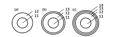
図1は本発明に係るローラ形状の帯電部材(以下、「帯電ローラ」ともいう)の概略構成図である。図1(a)に示すように、導電性の軸芯体11の外周に第1の導電層12が設けられている。この場合、第1の導電層12は、本発明のイオン導電性樹脂を含有している。図1(b)に示すように、第1の導電層12の外周上に第2の導電層13を設けてもよい。さらに、図1(c)に示すように、本発明の効果を損なわない範囲で、最外層14を設けてもよい。導電層が複数設けられている場合、いずれかの層、もしくは全ての層が本発明のイオン導電性樹脂を含有していればよい。
FIG. 1 is a schematic configuration diagram of a roller-shaped charging member (hereinafter also referred to as “charging roller”) according to the present invention. As shown in FIG. 1A, the first
[導電性の軸芯体]
導電性の軸芯体11は、軸芯体を介して帯電ローラの表面に給電するために導電性を有する。
[Conductive shaft core]
The conductive
[イオン導電性樹脂を含有する導電層]
以下、イオン導電性樹脂を含有する導電層について詳細に説明する。
[Conductive layer containing ionic conductive resin]
Hereinafter, the conductive layer containing an ion conductive resin will be described in detail.
<イオン導電性樹脂>
イオン導電性樹脂が、イオン伝導を発現するためには、まず、イオン解離、すなわち、イオン交換基がカチオンとアニオンとの電離を生じさせる必要がある。そのためには、通常、電解質を極性溶媒に溶解させ、発生するイオンキャリア(カチオンあるいはアニオン)が単独で存在できる状態にする。そして、このイオンキャリアが、再びイオン交換基と再結合せずに、安定して移動できる状態でなければならない。極性溶媒中では、溶媒分子によってイオンキャリアの安定化がなされる。
<Ion conductive resin>
In order for the ion conductive resin to exhibit ionic conduction, first, ion dissociation, that is, an ion exchange group needs to cause ionization of a cation and an anion. For this purpose, the electrolyte is usually dissolved in a polar solvent so that the generated ion carrier (cation or anion) can exist alone. And this ion carrier must be in the state which can move stably, without recombining with an ion exchange group again. In polar solvents, the ion carriers are stabilized by solvent molecules.
一方で、電子写真用導電性部材の導電層の構成するイオン導電性樹脂は、イオンの解離とイオンの移動とを、固体のイオン導電性樹脂中で生じさせる必要がある。つまり、イオン導電性樹脂の構造が、極性溶媒に代わるイオン解離作用を有する構造と、イオンキャリアを安定化させる構造とを有する必要がある。 On the other hand, the ionic conductive resin constituting the conductive layer of the electrophotographic conductive member needs to cause dissociation of ions and movement of ions in the solid ionic conductive resin. That is, the structure of the ion conductive resin needs to have a structure having an ion dissociation action instead of a polar solvent and a structure stabilizing the ion carrier.
<<イオン解離作用を有する構造>>
固体中において、イオン導電性樹脂中でイオン解離させるためには、イオン交換基と極性溶媒に代わる分子との親和性を持たせるために、イオン導電性樹脂中の水和量を大きくする必要があると考えられる。イオン交換基とは、例えば、スルホン酸基、カルボン酸基、リン酸基、ホスホン酸基、亜ホスホン酸基、第四級アンモニウム塩基が挙げられる。
<< Structure with ion dissociation action >>
In order to dissociate ions in an ion conductive resin in a solid, it is necessary to increase the amount of hydration in the ion conductive resin in order to have an affinity between an ion exchange group and a molecule instead of a polar solvent. It is believed that there is. Examples of the ion exchange group include a sulfonic acid group, a carboxylic acid group, a phosphoric acid group, a phosphonic acid group, a phosphonous acid group, and a quaternary ammonium base.
そして、本発明では、イオン解離性が高く、少ない添加量であっても低抵抗化が可能な、スルホン酸基、第四級アンモニウム塩基のいずれかであることが必要である。 In the present invention, it is necessary to be either a sulfonic acid group or a quaternary ammonium base that has high ion dissociation properties and can reduce resistance even with a small addition amount.
また、イオン交換基の導入量としては、イオン導電性樹脂の体積抵抗率が、中抵抗領域(体積抵抗率が1×10²Ω・cm〜1×10¹¹Ω・cm)になるような量が好ましい。さらに、スルホン酸基、または、第四級アンモニウム塩基のイオン解離によってイオン導電性を発生するイオン導電性樹脂においては、水分子が十分に存在する状態において、十分な導電性能を得られることが分かっている。 The amount of ion exchange groups introduced is such that the volume resistivity of the ion conductive resin is in the middle resistance region (volume resistivity is 1 × 10 2 Ω · cm to 1 × 10 11 Ω · cm). Is preferred. Furthermore, it has been found that an ionic conductive resin that generates ionic conductivity by ionic dissociation of a sulfonic acid group or a quaternary ammonium base can obtain sufficient conductive performance in a state where water molecules are sufficiently present. ing.
つまり、固体中において、イオン導電性樹脂のイオン導電性を保持させるためには、イオン導電性樹脂中の保水量が重要な要素になると考えられる。しかしながら、イオン導電性樹脂中の保水量は環境依存性が大きく、低温低湿環境において、十分な導電性を得ることが難しい場合があった。 That is, in order to maintain the ionic conductivity of the ion conductive resin in the solid, it is considered that the water retention amount in the ion conductive resin is an important factor. However, the amount of water retained in the ion conductive resin is highly dependent on the environment, and it may be difficult to obtain sufficient conductivity in a low temperature and low humidity environment.
そこで、本発明者らは、上記課題を解決する手段として、イオン導電性樹脂が低湿環境に晒された場合であっても、イオン導電性樹脂中のイオン交換基周辺の水和量が維持されるような分子設計を行うことを試みた。 Therefore, as a means for solving the above problems, the present inventors maintain the amount of hydration around the ion exchange groups in the ion conductive resin even when the ion conductive resin is exposed to a low humidity environment. I tried to design such a molecule.
すなわち、イオン交換基周辺の水和量を水酸基によって増加させるためには、イオン交換基と水酸基とができるだけ近接していることが好ましいと考えられる。ところが、イオン交換基と水酸基とが、ごく近傍に位置し、両者の間に結合エネルギーの大きな水素結合が形成されると、イオン交換基のイオン解離作用が失われ、イオン導電性が得られなくなることが予想される。 That is, in order to increase the amount of hydration around the ion exchange group by the hydroxyl group, it is considered preferable that the ion exchange group and the hydroxyl group are as close as possible. However, when an ion exchange group and a hydroxyl group are located very close to each other and a hydrogen bond having a large binding energy is formed between them, the ion dissociation action of the ion exchange group is lost and ionic conductivity cannot be obtained. It is expected that.
一方で、イオン交換基と水酸基との距離が大きくなると、水酸基の存在によって、イオン導電性樹脂全体の保水量が増加したとしても、イオン交換基周辺の水和量を増加させることはできず、イオン導電性の向上の効果は低いと予想される。 On the other hand, when the distance between the ion exchange group and the hydroxyl group is increased, even if the water retention amount of the entire ion conductive resin is increased due to the presence of the hydroxyl group, the amount of hydration around the ion exchange group cannot be increased. The effect of improving ionic conductivity is expected to be low.
そこで、本発明者らは、共有結合における結合距離(炭素−炭素間距離で約0.15nm、炭素−窒素間距離で約0.146nm、炭素−酸素間距離で約0.148nm、水素−酸素間距離で約0.095nm)と、水素結合における結合距離(水素−酸素間距離で約0.272nm)との関係を踏まえ、イオン交換基と水酸基との位置を最適化すべく、下記式(1)から式(4)で示される構造からなる群から選択される少なくとも1つの構造を含むイオン導電性樹脂について検討を行った。 Therefore, the present inventors have determined the bond distance in the covalent bond (carbon-carbon distance is about 0.15 nm, carbon-nitrogen distance is about 0.146 nm, carbon-oxygen distance is about 0.148 nm, hydrogen-oxygen. In order to optimize the position of the ion exchange group and the hydroxyl group based on the relationship between the bond distance in the hydrogen bond (approximately 0.072 nm in hydrogen distance) and the bond distance in the hydrogen bond (approximately 0.272 nm in hydrogen-oxygen distance), the following formula (1 ) To ion conductive resin containing at least one structure selected from the group consisting of structures represented by formula (4).
その結果、下記式(1)から式(4)で示される構造からなる群から選択される少なくとも1つの構造を分子内に有するイオン導電性樹脂は、低湿環境下においても電気抵抗値が上昇し難いことを見出した。 As a result, the ion conductive resin having at least one structure selected from the group consisting of structures represented by the following formulas (1) to (4) in the molecule has an increased electrical resistance value even in a low humidity environment. I found it difficult.
すなわち、下記式(1)、(2)、(3)および(4)で示される構造からなる群から選ばれる少なくとも1つの構造を分子内に有するイオン導電性樹脂は、水酸基が、イオン導電性樹脂中の水分子と水素結合を形成するため、イオン導電性樹脂自体の保水量が増す。加えて、イオン交換基は、水酸基の近傍に配置されているため、イオン交換基周辺の水和量が相乗的に増加する。その結果として、当該イオン導電性樹脂は、低温低湿環境においてもイオン伝導を十分に得られるものと考えられる。
また、上記式(1)〜(4)の中でも、式(1)の構造が特に好ましい。これは、イオン導電性樹脂中の保水量の観点から、イオン導電性樹脂の構造中で、孤立電子対と水分子との間で上記式(1)〜(4)中で最も強い水素結合を形成することができるためである。 Of the above formulas (1) to (4), the structure of the formula (1) is particularly preferable. This is because, from the viewpoint of the water retention amount in the ion conductive resin, the strongest hydrogen bond in the above formulas (1) to (4) is formed between the lone pair and the water molecule in the structure of the ion conductive resin. This is because it can be formed.
<<イオンキャリアを安定化させる構造>>
イオン交換基と解離したイオンキャリアが、導電層のイオン導電に十分に寄与するためには、イオンキャリアが導電層中を移動する最中に、再びイオン導電性樹脂が有するイオン交換基と再結合しないことが重要である。そのためには、イオン導電性樹脂中にイオンキャリアを安定化させる構造を導入する必要がある。
<< Structure to stabilize ion carrier >>
In order for the ion carrier dissociated from the ion exchange group to sufficiently contribute to the ionic conduction of the conductive layer, the ion carrier again recombines with the ion exchange group of the ion conductive resin while the ion carrier moves through the conductive layer. It is important not to. For this purpose, it is necessary to introduce a structure that stabilizes ion carriers in the ion conductive resin.
本発明では、イオンキャリアを安定化させる構造として、イオン導電性樹脂中に下記式(5)で示されるエチレンオキサイド構造を導入することが重要である。エチレンオキサイド構造は、その分子構造中に存在するエーテル結合によってイオンキャリアを安定化させることができる。さらに、エチレンオキサイド構造は、その分子構造中に、酸素原子に起因する極性帯を持つことから、カチオンと強い相互作用を有するために、イオン導電性を担うイオンキャリアとしては、アニオンよりもカチオンであるほうが、より安定化されると考えられる。
本発明に係るイオン導電性樹脂は、低温低湿環境下においても十分な導電性が必要なため、イオンキャリアを安定化させるエチレンオキサイド構造は、イオン交換基の近傍に存在することが好ましい。また、その結合形態としては、イオンキャリアを安定化するために、イオン交換基を有する構造の両端にある、下記式(6)の構造であることが好ましい。エチレンオキサイド構造の結晶化による高抵抗化を鑑み、下記式(6)の構造中のnは1以上、23以下の整数、mは1以上、18以下の整数であることが好ましい。同じ理由で、特に、nは1以上、4以下の整数、mは1以上、4以下の整数であることが望ましい。
一方で、式中X1、X2、X3、X4、X5の構造中のイオン交換基は、水酸基によるイオン交換基の安定化、イオン交換基周辺の水和量の増加を考慮すると、水素結合を生じない範囲で水酸基とより距離が近いほうが好ましいと考えられる。 On the other hand, the ion exchange groups in the structures of X 1 , X 2 , X 3 , X 4 , and X 5 in the formula take into account the stabilization of the ion exchange groups by the hydroxyl groups and the increase in the hydration amount around the ion exchange groups. It is considered that a distance closer to the hydroxyl group is preferable as long as no hydrogen bond is generated.
イオン交換基としては、エチレンオキサイドとの相互作用と考慮すると、カチオンがキャリアとなるスルホン酸基であることが好ましい。さらに、スルホン酸基のイオン解離性を向上させるために、電子供与性のあるアルキル基を介して結合させることがより好ましい。したがって、式(6)中で、R5がメチレン基、X5がスルホン酸基である構造を有することが好ましい。 In view of the interaction with ethylene oxide, the ion exchange group is preferably a sulfonic acid group in which a cation serves as a carrier. Furthermore, in order to improve the ionic dissociation property of the sulfonic acid group, it is more preferable to bond via an alkyl group having an electron donating property. Therefore, in formula (6), it is preferable to have a structure in which R 5 is a methylene group and X 5 is a sulfonic acid group.
<イオン導電性樹脂の製造方法>
本発明に係るイオン交換基を有するイオン導電性樹脂は、例えば、主剤、硬化剤、イオン導電剤を溶媒中で混合し、硬化させる方法を挙げることができる。ただし、この組み合わせの原料を用いる方法に限るものではない。
<Method for producing ion conductive resin>
Examples of the ion conductive resin having an ion exchange group according to the present invention include a method in which a main agent, a curing agent, and an ion conductive agent are mixed in a solvent and cured. However, it is not restricted to the method using the raw material of this combination.
<<主剤>>
本発明に係る主剤としては、例えば、2個以上のグリシジル基を有するエポキシ化合物を用いることが考えられる。エチレンオキサイドを構造中に含むエポキシ化合物は、例えば、アルカンジオールジグリシジルエーテル、ポリアルキレンジグリシジルエーテル、アルキルジグリシジルエーテル、(ポリプロピレンオキサイド−ポリエチレンオキサイド−ポリプロピレンオキサイド)ブロック共重合体のジグリシジルエーテルが挙げられる。なお、上記の化合物を単独で用いても、複数用いてもよい。一方で、エチレンオキサイド構造を有さないエポキシ化合物を用いる場合には、エチレンオキサイド構造を有する硬化剤を用いる必要がある。この場合、例えばアジピン酸が挙げられる。
<< Main agent >>
As the main agent according to the present invention, for example, an epoxy compound having two or more glycidyl groups may be used. Examples of the epoxy compound containing ethylene oxide in the structure include alkanediol diglycidyl ether, polyalkylene diglycidyl ether, alkyl diglycidyl ether, and (polypropylene oxide-polyethylene oxide-polypropylene oxide) block copolymer diglycidyl ether. It is done. The above compounds may be used alone or in combination. On the other hand, when using an epoxy compound having no ethylene oxide structure, it is necessary to use a curing agent having an ethylene oxide structure. In this case, for example, adipic acid can be mentioned.
特に、イオンキャリアを安定化させる効果が高いエチレンオキサイド構造を有するポリエチレングリコールジグリシジルエーテルを用いることが好ましい。もっとも好ましくは、エチレンオキサイドによる結晶化による高抵抗化の影響が小さい、エチレングリコールジグリシジルエーテルである。さらに、エチレングリコールジグリシジルエーテルの沸点は110度であり、イオン導電性樹脂の熱硬化温度よりも低い。そのため、ブリードやブルームなどの原因である、イオン導電性樹脂と共有結合を介して結合していない未反応物があっても、熱硬化過程で容易に除去することができるからである。 In particular, it is preferable to use polyethylene glycol diglycidyl ether having an ethylene oxide structure that has a high effect of stabilizing the ion carrier. Most preferably, it is ethylene glycol diglycidyl ether, which is less affected by high resistance due to crystallization with ethylene oxide. Furthermore, the boiling point of ethylene glycol diglycidyl ether is 110 degrees, which is lower than the thermosetting temperature of the ion conductive resin. Therefore, even if there is an unreacted substance that is not bonded to the ionic conductive resin via a covalent bond, which is a cause of bleeding or bloom, it can be easily removed in the thermosetting process.
<<硬化剤>>
本発明に係る硬化剤としては、例えば、アミン類、酸無水物類、多価フェノール類、チオール類、アルコール類が挙げられる。本発明では、イオン導電性樹脂構造中、孤立電子対と水分子との間が電気的に引き合って樹脂中の水和量を増加させ、さらに、架橋点となり、網目状構造を形成し、より水分子をイオン導電性樹脂内に保持できるため、アミン類を用いることが好ましいと考えられる。特に、導電性を確保するため、エチレンオキサイド構造を有するアミン類を用いることが好ましい。エチレンオキサイド構造を有するアミン類は、例えば、ポリアルキレングリコールビス2−アミノエチルエーテル、(ポリプロピレンオキサイド−ポリエチレンオキサイド−ポリプロピレンオキサイド)ブロック共重合体のビス2−アミノエチルエーテルが挙げられる。さらに好ましくは、十分な導電性を得るために、ポリエチレングリコールビス2−アミノエチルエーテルである。もっとも好ましくは、エチレンオキサイド構造の結晶化を鑑み、エチレングリコールビス2−アミノエチルエーテルである。上記の化合物を単独で用いても、複数用いてもよい。なお、チオール類、酸無水物類を硬化剤として用いる場合、硬化促進剤として、イミダゾールおよびアミン並びにその誘導体から成るアルカリ性化合物を少量使用することが望ましい。また、その硬化反応時において、本発明の効果を損なわない範囲で加熱して硬化反応を促進させることが好ましい。
<< Curing agent >>
Examples of the curing agent according to the present invention include amines, acid anhydrides, polyhydric phenols, thiols, and alcohols. In the present invention, in the ion conductive resin structure, the lone electron pair and the water molecule are electrically attracted to increase the amount of hydration in the resin, and further become a cross-linking point, forming a network structure, Since water molecules can be retained in the ion conductive resin, it is considered preferable to use amines. In particular, in order to ensure conductivity, it is preferable to use amines having an ethylene oxide structure. Examples of amines having an ethylene oxide structure include polyalkylene glycol bis-2-aminoethyl ether and bis-2-aminoethyl ether of a (polypropylene oxide-polyethylene oxide-polypropylene oxide) block copolymer. More preferably, it is polyethylene glycol bis 2-aminoethyl ether in order to obtain sufficient electrical conductivity. Most preferred is ethylene glycol bis 2-aminoethyl ether in view of crystallization of the ethylene oxide structure. The above compounds may be used alone or in combination. In addition, when using thiols and acid anhydrides as a curing agent, it is desirable to use a small amount of an alkaline compound composed of imidazole, amine and derivatives thereof as a curing accelerator. Moreover, at the time of the hardening reaction, it is preferable to accelerate the hardening reaction by heating within a range not impairing the effects of the present invention.
そして、上記硬化剤の配合量は、主剤100質量部に対して1質量部〜1000質量部の範囲に設定することが好ましい。より好ましくは、2質量部〜150質量部の範囲内である。また、硬化促進剤を用いる場合、主剤に対する硬化促進剤の配合量は、そのエポキシ化合物100質量部に対して0.01質量部〜20質量部の範囲に設定することが好ましい。より好ましくは、0.1質量部〜10質量部の範囲内である。すなわち、上記硬化剤や硬化促進剤が、上記規定の範囲未満であると、熱硬化が充分になされないからであり、逆に、上記硬化剤や硬化促進剤が、上記規定の範囲を超えると、硬化剤および硬化促進剤の未反応物がブリードしてしまうからである。 And it is preferable to set the compounding quantity of the said hardening | curing agent in the range of 1 mass part-1000 mass parts with respect to 100 mass parts of main agents. More preferably, it exists in the range of 2 mass parts-150 mass parts. Moreover, when using a hardening accelerator, it is preferable to set the compounding quantity of the hardening accelerator with respect to a main ingredient in the range of 0.01 mass part-20 mass parts with respect to 100 mass parts of the epoxy compound. More preferably, it exists in the range of 0.1 mass part-10 mass parts. That is, if the curing agent and the curing accelerator are less than the specified range, heat curing is not sufficiently performed. Conversely, if the curing agent and the curing accelerator exceed the specified range. This is because the unreacted material of the curing agent and the curing accelerator will bleed.
<<イオン導電剤>>
原料としてのイオン導電剤は、主剤、あるいは硬化剤と反応する反応性官能基と、第四級アンモニウム塩基、或いはスルホン酸基のいずれかのイオン交換基と、そのカウンターイオンであるキャリア分子とからなる。なお、反応性官能基とは、ハロゲン原子(フッ素、塩素、臭素およびヨウ素原子)、カルボキシル基、酸無水物のような酸基、水酸基、アミノ基、メルカプト基、アルコキシ基、ビニル基、グリシジル基、エポキシ基、ニトリル基、カルバモイル基のような官能基が挙げられ、主剤、あるいは硬化剤と反応する限りにおいて、いずれを用いてもかまわない。
<< Ion conductive agent >>
The ion conductive agent as a raw material is composed of a reactive functional group that reacts with the main agent or curing agent, an ion exchange group of either a quaternary ammonium base or a sulfonic acid group, and a carrier molecule that is a counter ion. Become. Reactive functional groups are halogen atoms (fluorine, chlorine, bromine and iodine atoms), carboxyl groups, acid groups such as acid anhydrides, hydroxyl groups, amino groups, mercapto groups, alkoxy groups, vinyl groups, glycidyl groups. And a functional group such as an epoxy group, a nitrile group, and a carbamoyl group, and any functional group may be used as long as it reacts with the main agent or the curing agent.
本発明に係るイオン導電剤の添加量は適宜設定することができ、主剤100質量部に対して、該イオン導電剤を0.5質量部以上20質量部以下の割合で配合することが好ましい。配合量が0.5質量部以上の場合には、導電剤添加による導電性の付与効果を容易に得ることができる。20質量部以下の場合には、電気抵抗の環境依存性を低減させることができる。 The addition amount of the ionic conductive agent according to the present invention can be appropriately set, and the ionic conductive agent is preferably blended at a ratio of 0.5 parts by mass or more and 20 parts by mass or less with respect to 100 parts by mass of the main agent. When the blending amount is 0.5 parts by mass or more, the effect of imparting conductivity by adding a conductive agent can be easily obtained. In the case of 20 parts by mass or less, the environmental dependency of electrical resistance can be reduced.
<<溶媒>>
本発明に係る溶媒は、硬化剤がアミン類、アルコール類、チオール類である場合はイソプロピルアルコール(以下、「IPA」ともいう)を用いることが好ましい。一方、硬化剤として酸無水物類を用いる場合は、溶媒と硬化剤との反応を防ぐため、エーテル系の溶媒、あるいはケトン系の溶媒を用いる必要がある。例としては、トルエン、ベンゼン、メチルエチルケトン、メチルイソプロピルブチルケトンが挙げられる。
<< solvent >>
As the solvent according to the present invention, it is preferable to use isopropyl alcohol (hereinafter also referred to as “IPA”) when the curing agent is an amine, an alcohol, or a thiol. On the other hand, when acid anhydrides are used as the curing agent, it is necessary to use an ether solvent or a ketone solvent in order to prevent the reaction between the solvent and the curing agent. Examples include toluene, benzene, methyl ethyl ketone, methyl isopropyl butyl ketone.
本発明に係る溶媒の配合量は、発明の効果を損なわない範囲で適宜設定できる。好ましくは、主剤、硬化剤、イオン導電剤のような原料が適切に混合できる配合量がよい。 The compounding quantity of the solvent which concerns on this invention can be suitably set in the range which does not impair the effect of invention. Preferably, the compounding quantity which can mix suitably a raw material like a main ingredient, a hardening | curing agent, and an ionic conductive agent is good.
<<他の成分>>
イオン導電性樹脂には、本発明の効果を損なわない範囲で、樹脂の配合剤として一般的に用いられている充填剤、軟化剤、加工助剤、粘着付与剤、粘着防止剤、分散剤、発泡剤を添加することができる。
<< other ingredients >>
In the ion conductive resin, a filler, a softening agent, a processing aid, a tackifier, an anti-tacking agent, a dispersant, which are generally used as a resin compounding agent, as long as the effects of the present invention are not impaired. A blowing agent can be added.
[導電性ローラの構成]
本発明のイオン導電性樹脂を図1(b)に示すような、第2の導電層13として用いた場合、第1の導電層12を形成するゴム成分としては、特に限定されるものではなく、電子写真用導電性部材の分野において公知のゴムを用いることができる。具体的には、エチレン−プロピレン−ジエン共重合体、スチレン−ブタジエン共重合ゴム(SBR)、シリコーンゴム、イソプレンゴム(IR)、ブチルゴム(BR)、クロロプレンゴム(CR)、エピクロルヒドリンホモポリマー、エピクロルヒドリン−エチレンオキサイド共重合体、エピクロルヒドリン−エチレンオキサイド−アリルグリシジルエーテル3元共重合体、アクリロニトリル−ブタジエン共重合体、アクリロニトリル−ブタジエン共重合体の水素添加物、アクリロニトリル-ブタジエン-メタクリル酸共重合体のようなカルボキシル化アクリロニトリル-ブタジエン共重合体、アクリルゴム、ウレタンゴム、アクリルゴム、ジエン系ゴム、シリコーンゴム、多硫化ゴム等が挙げられる。これらのゴム材料は、1種又は2種以上を組み合わせて用いてもよい。帯電ローラの材料としては、イオン導電剤や電子導電剤を分散させた際に、中抵抗領域の電気抵抗値を得やすい点を考慮すると、エピクロルヒドリン−エチレンオキサイド−アリルグリシジルエーテル3元共重合体又はアクリロニトリル−ブタジエン共重合体が好ましい。現像部材の材料としては、耐圧縮永久歪性を考慮すると、シリコーンゴム又はウレタンゴムが好ましい。
[Configuration of conductive roller]
When the ion conductive resin of the present invention is used as the second
本発明のイオン導電性樹脂を図1(b)に示すような、第1の導電層12として用いた場合、第2の導電層13は、電子写真用導電性部材の分野において公知の樹脂を用いることができる。具体的には、アクリル樹脂、ポリウレタン、ポリアミド、ポリエステル、ポリオレフィンおよびシリコーン樹脂が挙げられる。上記第2の導電層13を形成する樹脂に対して、必要に応じて、カーボンブラック、グラファイト、酸化錫、酸化亜鉛、酸化インジウム、酸化チタン、酸化錫―酸化アンチモン固溶体、酸化錫―酸化インジウム固溶体等を導電化処理した導電性金属酸化物、アルミニウム、銅、錫、ステンレス鋼等の各種導電性金属または合金、これらの導電性材料で被覆された絶縁性物質の微粉末、第四級アンモニウム塩のようなイオン交換性能を有するイオン導電剤、珪藻土、石英粉末、乾式シリカ、湿式シリカ、酸化チタン、酸化亜鉛、アルミノケイ酸、炭酸カルシウム等の非導電性充填剤を挙げることができる。
When the ion conductive resin of the present invention is used as the first
なお、図1(c)のように、第2の導電層13の外周に、発明の効果を損なわない範囲内で保護層としての最外層14を設けてもよい。
As shown in FIG. 1C, an
[電子写真装置]
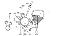
図2は、本発明に係る電子写真装置の概略図である。電子写真感光体201を帯電する帯電ローラ202、露光を行う潜像形成装置(不図示)、トナー像に現像する現像装置203、転写材204に転写する転写装置205、電子写真感光体上の転写トナーを回収するクリーニング装置207、トナー像を定着する定着装置206のような構成部材から構成される。電子写真感光体201は、導電性基体上に感光層を有する回転ドラム型である。電子写真感光体201は矢印の方向に所定の周速度(プロセススピード)で回転駆動される。帯電ローラ202は、電子写真感光体201に所定の力で押圧されることにより接触配置される。帯電ローラ202は、電子写真感光体201の回転に従い従動回転し、帯電用電源213から所定の直流電圧を印加することにより、電子写真感光体201を所定の電位に帯電する。電子写真感光体201に潜像を形成する潜像形成装置は、例えばレーザービームスキャナーのような露光装置が用いられる。
[Electrophotographic equipment]
FIG. 2 is a schematic view of an electrophotographic apparatus according to the present invention. A charging
一様に帯電された電子写真感光体201に、画像情報に対応して変調された露光光208を照射することによって、静電潜像が形成される。現像装置203は、電子写真感光体201に接触して配設されたローラ形状の現像部材((以下、「現像ローラ」ともいう)を有する。感光帯電極性と同極性に静電処理されたトナーを反転現像により、静電潜像をトナー像に可視化現像する。転写装置205は、接触式の転写ローラを有する。電子写真感光体201からトナー像を普通紙のような転写材204に転写する。尚、転写材204は、搬送部材を有する給紙システムにより搬送される。クリーニング装置207は、ブレード型のクリーニング部材および回収容器を有し、転写した後、電子写真感光体201上に残留する転写残トナーを機械的に掻き落として回収する。ここで、現像装置203にて転写残トナーを回収する現像同時クリーニング方式を採用することにより、クリーニング装置207を取り除くことも可能である。定着装置206は、加熱されたロールのような部材で構成され、転写されたトナー像を転写材204に定着し、機外に排出する。
An electrostatic latent image is formed by irradiating the uniformly charged electrophotographic
そして、本発明に係る電子写真装置は、電子写真感光体に接触配置された帯電部材、および、電子写真感光体に接触配置された現像部材のいずれか一方、または、両方に、本発明に係る電子写真用導電性部材が用いられてなるものである。 The electrophotographic apparatus according to the present invention relates to either or both of a charging member disposed in contact with the electrophotographic photosensitive member and a developing member disposed in contact with the electrophotographic photosensitive member. An electrophotographic conductive member is used.
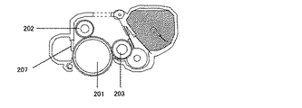
[プロセスカートリッジ]
図3はプロセスカートリッジの概略断面図である。図3に示したプロセスカートリッジは、電子写真感光体201、電子写真感光体201に接触して配置された帯電ローラ202、電子写真感光体201に接触して配置された現像ローラ203、および、クリーニング装置207等を含み、電子写真装置の本体に着脱可能に構成されている。そして、本発明に係るプロセスカートリッジは、現像ローラ202および帯電ローラ203の何れか一方、または両方に、本発明に係る電子写真用導電性部材が用いられてなるものである。
[Process cartridge]
FIG. 3 is a schematic sectional view of the process cartridge. The process cartridge shown in FIG. 3 includes an electrophotographic
(第二の実施の形態)
本発明の第二の実施の形態は、燃料電池用電解質膜である。
(Second embodiment)
The second embodiment of the present invention is a fuel cell electrolyte membrane.
本発明に係るイオン導電性樹脂に、電極を配置することにより、膜電極接合体を作製することができる。この膜電極接合体は、本発明に係るイオン導電性樹脂と、それを挟んで対向する触媒電極(アノードおよびカソード)とから構成され、該触媒電極はガス拡散層上に触媒層が形成されている。この接合体の作製方法としては、特に制限はなく、公知の技術を用いることができる。例えば、白金、白金−ルテニウム合金、あるいはその微粒子をカーボンのような担持体上に分散担持させたものを触媒とするガス拡散電極をイオン導電性樹脂に直接形成する方法、ガス拡散電極とイオン導電性樹脂とをホットプレスする方法、あるいは、接着液により接合する方法のような方法により作製できる。 A membrane electrode assembly can be produced by disposing an electrode on the ion conductive resin according to the present invention. This membrane electrode assembly is composed of an ion conductive resin according to the present invention and a catalyst electrode (anode and cathode) opposed to each other with the catalyst electrode formed on the gas diffusion layer. Yes. There is no restriction | limiting in particular as a preparation method of this conjugate | zygote, A well-known technique can be used. For example, a method in which a gas diffusion electrode is formed directly on an ion conductive resin using platinum, a platinum-ruthenium alloy, or fine particles dispersed and supported on a carrier such as carbon, a gas diffusion electrode and an ionic conductivity It can be produced by a method such as a method of hot-pressing with an adhesive resin or a method of bonding with an adhesive liquid.
また、本発明に係るイオン導電性樹脂や前記膜電極接合体を用いて、公知の手法により燃料電池を作製することができる。該燃料電池の構成の一例としては、前記膜電極接合体、該膜電極接合体を挟持する一対のセパレータ、セパレータに取り付けられた集電体、およびパッキンを備える構成が挙げられる。アノード極側のセパレータにはアノード極側開口部が設けられ、水素、メタノールのようなアルコール類のガス燃料または液体燃料が供給される。一方、カソード極側のセパレータにはカソード極側開口部が設けられ、酸素ガス、空気のような酸化剤ガスが供給される。 Moreover, a fuel cell can be produced by a known method using the ion conductive resin according to the present invention and the membrane electrode assembly. An example of the configuration of the fuel cell includes a configuration including the membrane electrode assembly, a pair of separators that sandwich the membrane electrode assembly, a current collector attached to the separator, and a packing. An anode electrode side opening is provided in the anode electrode side separator, and gas fuel or liquid fuel of alcohols such as hydrogen and methanol is supplied. On the other hand, the cathode pole side separator is provided with a cathode pole side opening, and is supplied with an oxidant gas such as oxygen gas and air.
以下、実施例により本発明を具体的に説明する。 Hereinafter, the present invention will be described specifically by way of examples.
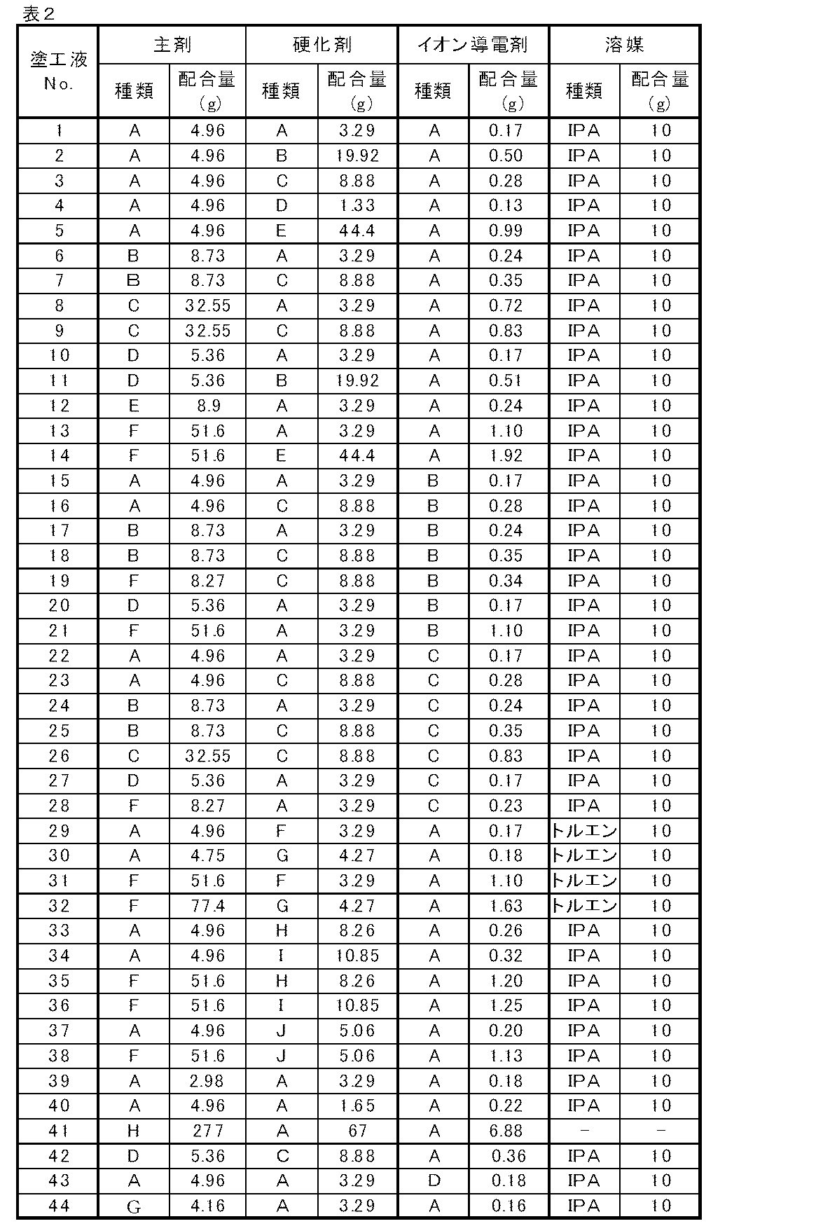
1.塗工液の調製;
<塗工液No.1〜44の調製>
表1−1〜表1−3に示した主剤、硬化剤およびイオン導電剤を、表2に示したような組み合わせ、および配合量にて、表2に併せて示した量の溶剤に混合し、大気中、室温で十分に撹拌し、塗工液No.1〜44を得た。
1. Preparation of coating solution;
<Coating liquid No. Preparation of 1-44>
The main agent, curing agent and ionic conductive agent shown in Table 1-1 to Table 1-3 are mixed in the amount of solvent shown in Table 2 in the combinations and blending amounts shown in Table 2. In the atmosphere, the mixture was sufficiently stirred at room temperature. 1-44 were obtained.
<塗工液No.45の調製>
2−ヒドロキシエチルアクリレート10g、メチルメタアクリレート60g、および下記式(7)に記載の第四級アンモニウム塩基重合体25gの配合量でモノマーを共重合させ、共重合体水溶液を得た。さらにこの共重合体水溶液に、グリセロールポリグリシジルエーテルを5g添加し、架橋硬化剤として2−メチルイミダゾールを0.1g加え、塗工液No.45を調製した。
Monomers were copolymerized in an amount of 10 g of 2-hydroxyethyl acrylate, 60 g of methyl methacrylate, and 25 g of a quaternary ammonium base polymer described in the following formula (7) to obtain a copolymer aqueous solution. Further, 5 g of glycerol polyglycidyl ether was added to this aqueous copolymer solution, and 0.1 g of 2-methylimidazole was added as a crosslinking curing agent. 45 was prepared.
<評価1> 樹脂薄膜の試験片の電気抵抗率の環境依存性の評価;
各塗工液から作成した樹脂薄膜の電気抵抗率の環境依存性を以下の方法により評価した。
<Evaluation 1> Evaluation of environmental dependency of electrical resistivity of test piece of resin thin film;
The environmental dependency of the electrical resistivity of the resin thin film prepared from each coating solution was evaluated by the following method.
(1−1)試験片の作成;
各塗工液をアルミニウム製のカップに入れ、温度160℃で20分間加熱して硬化させた後、アルミカップから硬化物を取り出し、電気抵抗値の測定用の試験片を作成した。なお、試験片の膜厚は0.5mmとした。
(1-1) Preparation of test piece;
Each coating solution was put in an aluminum cup and cured by heating at a temperature of 160 ° C. for 20 minutes, and then the cured product was taken out from the aluminum cup to prepare a test piece for measuring an electric resistance value. The film thickness of the test piece was 0.5 mm.
(1−2)試験片の電気抵抗値の測定;
上記で調製した試験片をガイドリンク付き電極に挟み、温度23℃/湿度50%R.H.環境(以降、「N/N環境」ともいう)下、および温度15℃/湿度10%R.H.環境(以降、「L/L環境」ともいう)下に置いて、直流200Vの電圧を印加し、各環境下における電気抵抗値を測定した。そして、得られた電気抵抗値から、各環境下における体積抵抗率を算出した。
(1-2) Measurement of electrical resistance value of test piece;
The test piece prepared above was sandwiched between electrodes with guide links, and the temperature was 23 ° C./humidity was 50% R.D. H. Environment (hereinafter also referred to as “N / N environment”), temperature 15 ° C./humidity 10% R.D. H. A voltage of DC 200 V was applied under an environment (hereinafter also referred to as “L / L environment”), and an electrical resistance value under each environment was measured. And the volume resistivity in each environment was computed from the obtained electrical resistance value.
また、電気抵抗率の環境依存性を確認するため、L/L環境下における電気抵抗値と、N/N環境下における電気抵抗値との比の対数を算出する。この値を環境変動桁とする。 Further, in order to confirm the environmental dependency of the electrical resistivity, the logarithm of the ratio between the electrical resistance value in the L / L environment and the electrical resistance value in the N / N environment is calculated. This value is used as the environmental fluctuation digit.
結果を下記表3−1及び表3−2に示す。また、本発明に係る構造(1)〜(6)の中で、各試験片を構成している樹脂が含む構造を、表3−1及び表3−2に併せて示す。 The results are shown in Tables 3-1 and 3-2 below. Moreover, the structure which resin which comprises each test piece contains among structure (1)-(6) which concerns on this invention is combined with Table 3-1, and Table 3-2 is shown.
2.ゴムローラの作製;
2−1.ゴムローラNo.1の作成;
<エピクロルヒドリンゴム組成物の調製>
表4に示す種類と量の各材料をオープンロールにて混合し、A練りゴム組成物を調製した。
2. Production of rubber rollers;
2-1. Rubber roller No. Creation of 1;
<Preparation of epichlorohydrin rubber composition>
The types and amounts of materials shown in Table 4 were mixed with an open roll to prepare an A-kneaded rubber composition.
次に、上記A練りゴム組成物176質量部に対して、表5に示す種類と量の各材料をオープンロールにて混合し、未加硫ゴム組成物を調製した。 Next, with respect to 176 parts by mass of the A-kneaded rubber composition, materials of the types and amounts shown in Table 5 were mixed with an open roll to prepare an unvulcanized rubber composition.
<導電性弾性層(エピクロルヒドリンゴム層)の形成>
導電性の軸芯体として外径φ6mm、長さ258mmのステンレス棒の芯金を用いた。クロスヘッド押し出し機に芯金の供給機構、導電性ローラの排出機構を有する装置を用意し、芯金の搬送速度を60mm/sec、クロスヘッドには内径がφ(直径)12.5mmのダイスを取り付け、押し出し機とクロスヘッドとを80℃に調整した。押し出し機から上記の未加硫ゴム組成物を熔融押し出しし、クロスヘッドに供給した芯金の周囲に未加硫ゴム組成物の層を形成した。
<Formation of conductive elastic layer (epichlorohydrin rubber layer)>
As the conductive shaft core, a stainless bar core with an outer diameter of 6 mm and a length of 258 mm was used. A device having a core bar supply mechanism and a conductive roller discharge mechanism is prepared in the crosshead extruder, and the core bar transport speed is 60 mm / sec, and the crosshead is a die having an inner diameter of 12.5 mm. The attachment, extruder and crosshead were adjusted to 80 ° C. The unvulcanized rubber composition was melt extruded from an extruder, and a layer of the unvulcanized rubber composition was formed around the core bar supplied to the crosshead.
次に、170℃の熱風加硫炉中に未加硫ゴム組成物の層で周面が被覆された芯金を投入し、60分間加熱して当該未加硫ゴム組成物の層を架橋させて導電層とした。その後、導電層の長さが228mmになるように端部を切断、除去した。最後に、導電層の表面を回転砥石で研磨し、中央部直径12.2mm、中央部から左右90mm端部側の平均直径12.0mmのクラウン形状に成形し導電性弾性層を備えたゴムローラNo.1を得た。 Next, a core metal whose peripheral surface is coated with a layer of an unvulcanized rubber composition is placed in a hot air vulcanization furnace at 170 ° C. and heated for 60 minutes to crosslink the layer of the unvulcanized rubber composition. Thus, a conductive layer was obtained. Thereafter, the end portion was cut and removed so that the length of the conductive layer was 228 mm. Finally, the surface of the conductive layer is polished with a rotating grindstone and molded into a crown shape having a central diameter of 12.2 mm and an average diameter of 12.0 mm from the central portion to the left and right ends of 90 mm. . 1 was obtained.
2−2.ゴムローラNo.2の作成;
A練りゴム組成物の原料を表6に示す組成に変更し、この練りゴム組成物177質量部に対して、表7に示す種類と量の各材料をオープンロールにて混合し未加硫ゴム組成物を得た。この未加硫ゴム組成物を用いた以外は、ゴムローラNo.1と同様にしてエピクロルヒドリンゴム層を備えたゴムローラNo.2を得た。
2-2. Rubber roller No. Creation of two;
The raw material of the A kneaded rubber composition was changed to the composition shown in Table 6, and each kind and amount of the materials shown in Table 7 was mixed with an open roll with respect to 177 parts by mass of the kneaded rubber composition to obtain an unvulcanized rubber. A composition was obtained. Except for using this unvulcanized rubber composition, rubber roller No. In the same manner as in No. 1, rubber roller No. 1 equipped with an epichlorohydrin rubber layer was prepared. 2 was obtained.
2−3.ゴムローラNo.3の作成;
導電性の軸芯体として外径8mm(SUM22材)、長さ258mmのステンレス棒の芯金を用いた。導電層および芯金の接着剤として、プライマーを塗布、焼付けし、この芯金を内径12mmの円筒状金型に同心となるように配置した。次に、下記表8に記載の原料を金型内に形成されたキャビティに注入し、130℃で60分加熱して硬化させた。その後室温に冷却して脱型後、200℃で4時間の2次加硫を行い、膜厚が3.0mmのシリコーンゴム層を有するゴムローラNo.3を作成した。
2-3. Rubber roller No. Creation of 3;
As the conductive shaft core body, a stainless bar core metal having an outer diameter of 8 mm (SUM22 material) and a length of 258 mm was used. A primer was applied and baked as an adhesive for the conductive layer and the cored bar, and this cored bar was placed concentrically with a cylindrical mold having an inner diameter of 12 mm. Next, the raw materials described in Table 8 below were poured into cavities formed in the mold and cured by heating at 130 ° C. for 60 minutes. Then, after cooling to room temperature and demolding, secondary vulcanization was performed at 200 ° C. for 4 hours, and rubber roller No. 1 having a silicone rubber layer with a thickness of 3.0 mm was obtained. 3 was created.
3.帯電ローラの作成;
(実施例1)
帯電ローラNo.1の作成、および評価;
塗工液No.1を、ゴムローラNo.1の外周面上に1回ディッピング塗布し、常温で30分間以上風乾し、次いで80℃に設定した熱風循環乾燥機にて1時間乾燥し、更に160℃に設定した熱風循環乾燥機にて3時間乾燥した。
3. Creating a charging roller;
Example 1
Charging roller No. Creation and evaluation of 1;
Coating liquid No. 1 is a rubber roller No. 1 dipping coating on the outer peripheral surface of 1 and air drying at room temperature for 30 minutes or more, then drying for 1 hour in a hot air circulating dryer set at 80 ° C., and further 3 in a hot air circulating dryer set at 160 ° C. Dry for hours.
ディッピング塗布浸漬時間は9秒、ディッピング塗布引き上げ速度は、初期速度が20mm/s、最終速度が2mm/sになるように調節し、20mm/sから2mm/sの間は、時間に対して直線的に速度を変化させた。以上のようにして、エピクロルヒドリンゴム導電層の外周に、イオン導電性樹脂含有層を有する帯電ローラNo.1を作製した。 The dipping coating dipping time is 9 seconds, and the dipping coating lifting speed is adjusted so that the initial speed is 20 mm / s and the final speed is 2 mm / s, and between 20 mm / s and 2 mm / s is linear with respect to time. The speed was changed. As described above, the charging roller No. 1 having the ion conductive resin-containing layer on the outer periphery of the epichlorohydrin rubber conductive layer. 1 was produced.
<評価2>帯電ローラの電気抵抗率の環境依存性の評価;
図4に、本発明に用いた帯電ローラの電流値測定機の概略構成図を示す。図4の様に、電子写真方式の画像形成装置に用いた場合の使用状態と同様の荷重で、感光体と同じ曲率の円柱形金属42に当接させて通電したときの電流値を測定する。図4(a)において43aと43bは重りに固定された軸受けであり、帯電ローラ41の導電性の軸芯体11の両端に鉛直下方向に押す応力を印加する。帯電ローラ41の鉛直下方向には、帯電ローラ41と平行に円柱形金属42が位置している。そして、図示しない駆動装置により円柱形金属42を回転させながら、図4(b)の様に帯電ローラ41を軸受け43aと43bとにより円柱形金属42へ押し当てる。使用状態の感光体ドラムと同様の回転速度で円柱形金属42を回転させ、帯電ローラ41を従動回転させながら、電源44によって直流電圧−200Vを印加する。電圧を印加して2秒後から、円柱形金属42から流れ出てくる電流の時間平均を電流計Aで測定し、5秒間測定した結果の時間平均から、電気抵抗値を算出する。
<Evaluation 2> Evaluation of the environmental dependency of the electrical resistivity of the charging roller;
FIG. 4 is a schematic configuration diagram of a charging roller current value measuring machine used in the present invention. As shown in FIG. 4, the current value is measured when a current is applied to a
このような装置を用いて、N/N環境下に48時間放置して順化させた帯電ローラNo.1、および、L/L環境に48時間放置して順化させた帯電ローラNo.1の各々に対して、直流200Vの電圧を印加して電気抵抗値を測定した。そして、測定して得られた電気抵抗値から、それぞれの環境下における体積抵抗率を算出した。また、環境変動の影響を確認するため、L/L環境下における電気抵抗値と、N/N環境下における電気抵抗値との比の対数を算出する。log(N/N環境での電気抵抗値)/(L/L環境下での電気抵抗値)。この値を環境変動桁とする。 Using such an apparatus, the charging roller No. 1 was allowed to acclimatize for 48 hours in an N / N environment. 1 and charging roller No. 1 which was allowed to acclimate for 48 hours in an L / L environment. A voltage of DC 200V was applied to each of 1 and the electrical resistance value was measured. And the volume resistivity in each environment was computed from the electrical resistance value obtained by measuring. Further, in order to confirm the influence of environmental fluctuation, the logarithm of the ratio between the electrical resistance value under the L / L environment and the electrical resistance value under the N / N environment is calculated. log (electric resistance value in N / N environment) / (electric resistance value in L / L environment). This value is used as the environmental fluctuation digit.
<評価3>ブリード評価;
帯電ローラをポリエチレンテレフタラート(PET)シート上に置き、帯電ローラの両端の軸に各々、500gの荷重をかけて、帯電ローラの表面をPETシートに押し付けた。温度40℃/湿度95%R.H.環境下にて、この状態を2週間維持した。その後、帯電ローラをPETシート上から取り除き、PETシート表面の帯電ローラ表面が押し付けられていた部分を、光学顕微鏡(10倍)で観察した。そして、帯電ローラからのブリード物の付着の有無を観察し、下記の基準に基づいて評価した。
<Evaluation 3> Bleed evaluation;
The charging roller was placed on a polyethylene terephthalate (PET) sheet, and a load of 500 g was applied to the shafts at both ends of the charging roller to press the surface of the charging roller against the PET sheet. Temperature 40 ° C./Humidity 95% R.D. H. This state was maintained for 2 weeks under the environment. Thereafter, the charging roller was removed from the PET sheet, and the portion of the PET sheet surface where the charging roller surface was pressed was observed with an optical microscope (10 times). And the presence or absence of adhesion of the bleed material from the charging roller was observed and evaluated based on the following criteria.
[ブリード評価ランク]
A:ブリードが観察されない。
B:一部に軽微なブリード物の付着が観察される。
C:当接部の全面にブリード物の付着が観察される。
[Bleed rating rank]
A: Bleed is not observed.
B: A slight bleed adherence is observed in part.
C: Adhesion of bleed material is observed on the entire surface of the contact portion.
<評価4>画像評価
<<評価4−1>>
L/L環境下に48時間放置し、当該環境に順化させた帯電ローラを電子写真画像の形成に用いた。帯電ローラの帯電能力が不足した場合、ハーフトーン画像には、横スジが生じる。そこで、ハーフトーン画像への横スジの発生状況を観察することで、L/L環境における帯電ローラの帯電能力を評価した。
<Evaluation 4> Image evaluation << Evaluation 4-1 >>
A charging roller that was left in an L / L environment for 48 hours and acclimated to the environment was used to form an electrophotographic image. When the charging ability of the charging roller is insufficient, a horizontal stripe is generated in the halftone image. Therefore, the charging capability of the charging roller in the L / L environment was evaluated by observing the occurrence of horizontal streaks on the halftone image.
ここで、ハーフトーン画像とは、全面黒画像を出力する場合に比べてレーザー光量を35%に弱め、帯電電位が全面黒画像と全面白画像との中間となる様な画像を指す。 Here, the halftone image refers to an image in which the amount of laser light is weakened to 35% as compared with the case where a full-color black image is output, and the charging potential is intermediate between the full-color black image and the full-color white image.
本評価においては、電子写真装置として、レーザープリンター(商品名:Laserjet 4700dn、HP社製)のプロセススピードを300mm/secに改造したものを用いた。また、当該レーザープリンターの印字密度は600dpiである。 In this evaluation, a laser printer (trade name: Laserjet 4700dn, manufactured by HP) with a modified process speed of 300 mm / sec was used as the electrophotographic apparatus. The printing density of the laser printer is 600 dpi.
具体的な評価方法としては、まず、被評価対象物としての帯電ローラを、上記レーザープリンター用プロセスカートリッジに装着し、このプロセスカートリッジを上記レーザープリンターに装填した。そして、A4サイズの紙上に、サイズが4ポイントのアルファベット「E」の文字が、印字濃度が1%となるように印字される電子写真画像を40000枚出力した。なお、電子写真画像の形成は、電子写真画像を2枚連続して出力する度に、電子写真装置の回転を2秒間停止させる間欠モードにて行った。そして、40000枚の電子写真画像の出力後、レーザープリンターからプロセスカートリッジを取り出し、当該プロセスカートリッジから帯電ローラを取り外して、表面を水で洗浄した。洗浄した帯電ローラを、再びプロセスカートリッジに装着し、当該プロセスカートリッジを上記レーザープリンターに装填して、上記と同様にして40000枚の電子写真画像を出力し、次いで、ハーフトーン画像を1枚出力した。このハーフトーン画像を目視で観察し、帯電ローラの帯電能力の低下に起因する横スジ状の欠陥の発生の有無を下記の基準により評価した。 As a specific evaluation method, first, a charging roller as an object to be evaluated was mounted on the process cartridge for the laser printer, and this process cartridge was mounted on the laser printer. Then, 40000 electrophotographic images were printed on an A4 size paper on which letters of the letter “E” having a size of 4 points were printed at a print density of 1%. The electrophotographic image was formed in an intermittent mode in which the rotation of the electrophotographic apparatus was stopped for 2 seconds every time two electrophotographic images were output continuously. Then, after outputting 40,000 electrophotographic images, the process cartridge was taken out from the laser printer, the charging roller was removed from the process cartridge, and the surface was washed with water. The washed charging roller is mounted again on the process cartridge, the process cartridge is loaded on the laser printer, and 40,000 electrophotographic images are output in the same manner as described above, and then one halftone image is output. . This halftone image was visually observed, and the presence or absence of horizontal streak-like defects caused by the decrease in charging ability of the charging roller was evaluated according to the following criteria.
A:ハーフトーン画像に横スジ状の画像欠陥が観察されない。
B:ハーフトーン画像のごく一部に軽微な横スジ状の画像欠陥が観察される。
C:ハーフトーン画像の一部に横スジ状の画像欠陥が観察されるが、目立たない。
D:ハーフトーン画像の一部に横スジ状の画像欠陥が観察され、目立つ。
A: No horizontal streak-like image defect is observed in the halftone image.
B: A slight horizontal streak-like image defect is observed in a small part of the halftone image.
C: A horizontal streak-like image defect is observed in a part of the halftone image, but is not conspicuous.
D: A horizontal streak-like image defect is observed in a part of the halftone image and is conspicuous.
<<評価4−2>>
L/L環境下に48時間放置し、当該環境に順化させた帯電ローラを電子写真画像の形成に供した。帯電ローラの帯電能力が不足し、感光体の帯電が不均一となったときに、ハーフトーン画像には、斑点状の欠陥が生じることがある。
<< Evaluation 4-2 >>
The charging roller which was left in an L / L environment for 48 hours and was acclimated to the environment was used for forming an electrophotographic image. When the charging ability of the charging roller is insufficient and the photosensitive member becomes non-uniformly charged, spotted defects may occur in the halftone image.
本評価においては、電子写真装置として、レーザープリンター(商品名:Laserjet P4515n、HP社製)を用意した。当該レーザープリンターのプロセススピードは370mm/sec、印字密度は1200dpiである。 In this evaluation, a laser printer (trade name: Laserjet P4515n, manufactured by HP) was prepared as an electrophotographic apparatus. The laser printer has a process speed of 370 mm / sec and a printing density of 1200 dpi.
具体的な評価方法としては、まず、被評価対象物としての帯電ローラを、上記レーザープリンター用プロセスカートリッジに装着した。そして、このプロセスカートリッジは、帯電ローラと電子写真感光体との間に電圧を外部から印加できるように改造した。 As a specific evaluation method, first, a charging roller as an object to be evaluated was mounted on the process cartridge for laser printer. This process cartridge was modified so that a voltage could be applied between the charging roller and the electrophotographic photosensitive member from the outside.
このプロセスカートリッジを上記レーザープリンターに装填し、帯電ローラと電子写真感光体との間に、−600Vの直流電圧、Vpp(peak to peak)=1600V、および、周波数=3000Hzの交流電圧を印加しつつ、電子写真画像を40000枚出力した。ここで、電子写真画像は、感光体の回転方向に幅2ドット、間隔176ドットの横線を描く電子写真画像とした。 The process cartridge is loaded in the laser printer, and a DC voltage of −600 V, Vpp (peak to peak) = 1600 V, and an AC voltage of frequency = 3000 Hz are applied between the charging roller and the electrophotographic photosensitive member. 40000 electrophotographic images were output. Here, the electrophotographic image was an electrophotographic image in which a horizontal line having a width of 2 dots and an interval of 176 dots was drawn in the rotation direction of the photosensitive member.
なお、電子写真画像の形成は、電子写真画像を1枚出力する度に、電子写真装置の回転を2秒間停止させるような間欠モードにて行った。 The electrophotographic image was formed in an intermittent mode in which the rotation of the electrophotographic apparatus was stopped for 2 seconds every time one electrophotographic image was output.
40000枚の電子写真画像の出力後、ハーフトーン画像を出力した。その際、帯電ローラと電子写真感光体との間に印加する交流電圧を、1枚のハーフトーン画像を出力する度に、Vpp=1200Vから上昇させ、ハーフトーン画像から、斑点状の欠陥が消失するまでハーフトーン画像の出力を続けた。なお、このときの交流電圧の周波数は2931Hzとした。そして、斑点状の欠陥がハーフトーン画像から焼失したときの交流電圧を評価4−2の結果として記載した。この電圧の値が小さい程、帯電能力が相対的に高い帯電ローラであるといえる。 After outputting 40,000 electrophotographic images, a halftone image was output. At that time, every time a halftone image is output, the AC voltage applied between the charging roller and the electrophotographic photosensitive member is increased from Vpp = 1200 V, and spotted defects disappear from the halftone image. The halftone image output was continued until In addition, the frequency of the alternating voltage at this time was 2931 Hz. And the alternating voltage when a spot-like defect burned out from a halftone image was described as a result of evaluation 4-2. It can be said that the smaller the value of this voltage is, the higher the charging ability of the charging roller.
(実施例2〜40)
帯電ローラ2〜40の作成、および評価;
塗工液No.1を表9−1及び表9−2に記載の塗工液に変更した以外は、帯電ローラNo.1と同様にして帯電ローラNo.2〜40を作成し、評価した。
(Examples 2 to 40)
Creation and evaluation of charging rollers 2-40;
Coating liquid No. 1 was changed to the coating liquid described in Table 9-1 and Table 9-2. In the same manner as in No. 1, the charging roller no. 2 to 40 were created and evaluated.
(実施例41〜46)
帯電ローラ41〜46の作成、および評価;
ゴムローラ2を用い、かつ、表9−1及び表9−2に記載の塗工液に変更した以外は、帯電ローラNo.1と同様にして帯電ローラNo.41〜46を作製し、評価2〜評価4に供した。
(Examples 41 to 46)
Creation and evaluation of charging rollers 41-46;
Except for using the rubber roller 2 and changing to the coating liquid described in Table 9-1 and Table 9-2, the charging roller No. In the same manner as in No. 1, the charging roller no. 41-46 were produced and used for Evaluation 2 to Evaluation 4.
(実施例47)
帯電ローラ47の作成、および評価;
導電性の軸芯体として外径φ6mm、長さ258mmのステンレス棒の芯金を用意した。そして、導電層および芯金の接着剤として、芯金の左端部を基準に40mmから248mmの領域にプライマーを塗布し、焼付けた。この芯金を内径16mmの円筒状金型に同心となるように配置した。次に、塗工液No.41を金型内に形成されたキャビティに注入し、金型を加熱して80℃で1時間、160℃で3時間加硫硬化し、脱型して、芯金の周面に導電層が形成されてなる帯電ローラNo.47を作成した。
(Example 47)
Creation and evaluation of charging roller 47;
As a conductive shaft core body, a stainless bar core bar having an outer diameter of φ6 mm and a length of 258 mm was prepared. Then, as an adhesive for the conductive layer and the cored bar, a primer was applied to an area of 40 mm to 248 mm based on the left end of the cored bar and baked. This cored bar was placed concentrically with a cylindrical mold having an inner diameter of 16 mm. Next, coating liquid No. 41 is injected into the cavity formed in the mold, and the mold is heated and cured at 80 ° C. for 1 hour and at 160 ° C. for 3 hours, demolded, and a conductive layer is formed on the peripheral surface of the core metal. The formed charging roller No. 47 was created.
(実施例48)
帯電ローラNo.48の作成、および評価;
帯電ローラNo.1の導電層上に、以下の方法にて、保護層を設けた。
(Example 48)
Charging roller No. 48 creation and evaluation;
Charging roller No. A protective layer was provided on one conductive layer by the following method.
カプロラクトン変性アクリルポリオール溶液にメチルイソブチルケトンを加え、固形分が10質量%となるように調整した。前述のアクリルポリオール溶液の固形分100質量部に対して、カーボンブラック(HAF)15質量部、針状ルチル型酸化チタン微粒子35質量部、変性ジメチルシリコーンオイル0.1質量部、およびヘキサメチレンジイソシアネート(HDI)とイソホロンジイソシアネート(IPDI)の各ブタノンオキシムブロック体の7:3の混合物、80.14質量部を入れ、混合溶液を調整した。このとき、ブロックHDIとブロックIPDIの混合物は、「NCO/OH=1.0」となるように添加した。 Methyl isobutyl ketone was added to the caprolactone-modified acrylic polyol solution to adjust the solid content to 10% by mass. 15 parts by mass of carbon black (HAF), 35 parts by mass of acicular rutile-type titanium oxide fine particles, 0.1 part by mass of modified dimethyl silicone oil, and hexamethylene diisocyanate (100 parts by mass of the solid content of the acrylic polyol solution described above) A 7: 3 mixture of each butanone oxime block of HDI) and isophorone diisocyanate (IPDI), 80.14 parts by mass, was added to prepare a mixed solution. At this time, the mixture of the block HDI and the block IPDI was added so that “NCO / OH = 1.0”.
450mLのガラス瓶に上記混合溶液210gと、分散メディアとしての平均粒径0.8mmのガラスビーズ200gとを混合し、ペイントシェーカー分散機を用いて24時間分散した。分散後、樹脂粒子として架橋タイプアクリル粒子(商品名:MR50G;綜研化学製)を5.44質量部(アクリルポリール100重量部に対して20重量部相当量)を添加した後、更に30分間分散して保護層形成用の塗料を得た。 In a 450 mL glass bottle, 210 g of the mixed solution and 200 g of glass beads having an average particle diameter of 0.8 mm as a dispersion medium were mixed and dispersed for 24 hours using a paint shaker disperser. After dispersion, 5.44 parts by mass of crosslinked acrylic particles (trade name: MR50G; manufactured by Soken Chemical Co., Ltd.) as resin particles were added (an equivalent of 20 parts by weight with respect to 100 parts by weight of acrylic polyol), and then for 30 minutes. A paint for forming a protective layer was obtained by dispersing.
得られた保護層形成用の塗料を、帯電ローラNo.1を1回ディッピングし、常温で30分間風乾した。次いで温度90℃に設定した熱風循環乾燥機にて1時間乾燥し、更に温度160℃に設定した熱風循環乾燥機にて1時間乾燥して、帯電ローラNo.1の導電層の周面に保護層を形成した。 The obtained coating material for forming the protective layer was charged with a charging roller No. 1 was dipped once and air dried at room temperature for 30 minutes. Subsequently, it was dried for 1 hour with a hot air circulating dryer set at a temperature of 90 ° C. and further dried for 1 hour with a hot air circulating dryer set at a temperature of 160 ° C. A protective layer was formed on the peripheral surface of one conductive layer.
なお、ディッピング塗布浸漬時間は9秒、ディッピング塗布引き上げ速度は、初期速度が20mm/s、最終速度が2mm/sになるように調節し、20mm/sから2mm/sの間は、時間に対して直線的に速度を変化させた。こうして得た帯電ローラを帯電ローラNo.48として、評価3〜評価4に供した。 The dipping coating immersion time is 9 seconds, and the dipping coating lifting speed is adjusted so that the initial speed is 20 mm / s and the final speed is 2 mm / s, and the time between 20 mm / s and 2 mm / s is relative to the time. The speed was changed linearly. The charging roller thus obtained was referred to as charging roller no. 48 was used for Evaluation 3 to Evaluation 4.
上記実施例1〜48の評価結果を表9−1及び表9−2に示す。 The evaluation results of Examples 1 to 48 are shown in Table 9-1 and Table 9-2.
(比較例1〜3)
帯電ローラNo.C−1〜C−3の作成、および評価;
塗工液No.42、43および44を用いた以外は、帯電ローラNo.1と同様にして帯電ローラNo.C−1〜C−3を作成し、評価2〜評価4に供した。
(Comparative Examples 1-3)
Charging roller No. Creation and evaluation of C-1 to C-3;
Coating liquid No. Except for using 42, 43 and 44, the charging roller no. In the same manner as in No. 1, the charging roller no. C-1 to C-3 were prepared and used for Evaluation 2 to Evaluation 4.
(比較例4)
帯電ローラNo.C−4の作成、および評価;
ゴムローラ1の導電性弾性層上に、乾燥膜厚が5μmとなるように、塗工液No.45をディッピング塗布した。次いで、塗工液No.45の塗膜を温度120℃にて7秒間加熱して硬化させて、帯電ローラNo.C−4を作成した。この帯電ローラNo.C−4を評価2〜評価4に供した。
(Comparative Example 4)
Charging roller No. Creation and evaluation of C-4;
On the conductive elastic layer of the rubber roller 1, the coating liquid No. 45 was dipped. Subsequently, coating liquid No. The coating film No. 45 was cured by heating at a temperature of 120 ° C. for 7 seconds. C-4 was created. This charging roller No. C-4 was subjected to Evaluation 2 to Evaluation 4.
比較例1〜4の結果を、表10に示す。 Table 10 shows the results of Comparative Examples 1 to 4.
4.現像ローラの作成;
(実施例49)
現像ローラNo.1の作成、および評価;
塗工液No.1を、ゴムローラNo.3の外周面上に1回ディッピング塗布し、常温(25℃)で30分間風乾し、次いで、温度80℃に設定した熱風循環乾燥機にて1時間乾燥し、更に、温度160℃に設定した熱風循環乾燥機にて3時間乾燥した。ディッピング塗布浸漬時間は9秒、ディッピング塗布引き上げ速度は、初期速度が20mm/s、最終速度が2mm/sになるように調節し、20mm/sから2mm/sの間は、時間に対して直線的に速度を変化させた。以上のようにして、シリコーンゴム層の外周に、イオン導電性樹脂含有層を有する現像ローラNo.1を作成した。この現像ローラNo.1を、評価3、および下記の評価5に供した。
4). Development roller creation;
(Example 49)
Development roller No. Creation and evaluation of 1;
Coating liquid No. 1 is a rubber roller No. 3 was applied once by dipping on the outer peripheral surface, air-dried at room temperature (25 ° C.) for 30 minutes, then dried in a hot air circulating drier set at a temperature of 80 ° C., and further set at a temperature of 160 ° C. It dried for 3 hours with the hot air circulation dryer. The dipping coating dipping time is 9 seconds, and the dipping coating lifting speed is adjusted so that the initial speed is 20 mm / s and the final speed is 2 mm / s, and between 20 mm / s and 2 mm / s is linear with respect to time. The speed was changed. As described above, the developing roller No. 1 having the ion conductive resin-containing layer on the outer periphery of the silicone rubber layer. 1 was created. This developing roller No. 1 was subjected to Evaluation 3 and Evaluation 5 below.
<評価5>
<画像評価>
L/L環境下に48時間放置し、当該環境に順化させた現像ローラを電子写真画像の形成に用いた。本評価に用いた電子写真装置は、レーザープリンター(商品名:LBP5400、キヤノン製)を、記録メディアの出力スピードを、150mm/secに改造したものを用いた。また、当該レーザープリンターの印字密度は、600dpiである。
<Evaluation 5>
<Image evaluation>
A developing roller that was left in an L / L environment for 48 hours and acclimated to the environment was used to form an electrophotographic image. The electrophotographic apparatus used for this evaluation was a laser printer (trade name: LBP5400, manufactured by Canon) with a recording medium output speed modified to 150 mm / sec. The printing density of the laser printer is 600 dpi.
また、現像ローラと、感光ドラムとの当接圧力、および進入量は、現像ローラ上のトナー被覆量が0.35mg/cm2となるように調整した。さらに、現像ローラから古いトナーを掻き落とし、現像ローラに新しいトナーを供給する軟質ウレタンスポンジ製のトナー供給ローラを設けた。 Further, the contact pressure between the developing roller and the photosensitive drum and the amount of entry were adjusted so that the toner coating amount on the developing roller was 0.35 mg / cm 2 . Further, a toner supply roller made of a soft urethane sponge that scrapes old toner from the developing roller and supplies new toner to the developing roller is provided.
具体的な評価方法としては、まず、被評価対象物としての帯電ローラを、上記レーザープリンター用プロセスカートリッジに装着し、このプロセスカートリッジを上記レーザープリンターに装填した。そして、感光ドラムの回転方向と垂直方向とに幅2ドット、間隔50ドットの横線を描くような電子写真画像を、20000枚連続して出力した。引き続いて、感光ドラムの回転方向と垂直方向に幅1ドット、間隔2ドットの横線を描くような電子写真画像を1枚出力し、この電子写真画像を、目視で観察し、以下の基準に基づき評価した。 As a specific evaluation method, first, a charging roller as an object to be evaluated was mounted on the process cartridge for the laser printer, and this process cartridge was mounted on the laser printer. Then, 20000 sheets of electrophotographic images that draw a horizontal line with a width of 2 dots and an interval of 50 dots in the rotation direction and the vertical direction of the photosensitive drum were continuously output. Subsequently, one electrophotographic image that draws a horizontal line with a width of 1 dot and an interval of 2 dots in the direction perpendicular to the rotation direction of the photosensitive drum is output. This electrophotographic image is visually observed and is based on the following criteria. evaluated.
A:画像濃度の変化がほとんどなく、現像ローラの回転周期に対応した画像不良が見られない。
B:画像濃度の変化がわずかに見られるが、現像ローラの回転周期に対応した画像不良が見られない。
C:画像濃度の変化が見られ、現像ローラの回転周期に対応した画像不良がかすかに認められる。
D:画像濃度の変化が大きく、現像ローラの回転周期に対応した画像不良が認められる。
A: There is almost no change in image density, and no image defect corresponding to the rotation cycle of the developing roller is observed.
B: A slight change in image density is seen, but no image defect corresponding to the rotation cycle of the developing roller is seen.
C: A change in image density is observed, and an image defect corresponding to the rotation period of the developing roller is faintly recognized.
D: The change in image density is large, and an image defect corresponding to the rotation period of the developing roller is recognized.
(実施例50)〜(実施例63)
現像ローラNo.2〜15の作成、および評価;
塗工液No.を表11に記載の塗工液に変更した以外は、現像ローラNo.1と同様に現像ローラNo.を作製し、評価した。
(Example 50) to (Example 63)
Development roller No. 2-15 creation and evaluation;
Coating liquid No. The developing roller No. was changed except that the coating solution was changed to the coating solution shown in Table 11. No. 1 as well as developing roller No. 1 Were made and evaluated.
実施例49〜63の結果を表11に示す。 The results of Examples 49 to 63 are shown in Table 11.
5.電解質膜の作成、および評価;
(実施例64)
以下の方法で燃料電池用の電解質膜を作製した。図5に本発明に係る燃料電池の概略構成図を示す。図5中で、51がイオン導電性樹脂膜、52が触媒シート、53が電極である。前記表1−1〜表1−3に示した主剤、硬化剤およびイオン導電剤を、表12に示した組み合わせ、および配合量にて、表12に併せて示した量の溶剤に混合し、大気中、室温(25℃)で十分に撹拌し、塗工液No.46を得た。
5. Creation and evaluation of electrolyte membranes;
(Example 64)
An electrolyte membrane for a fuel cell was produced by the following method. FIG. 5 shows a schematic configuration diagram of a fuel cell according to the present invention. In FIG. 5, 51 is an ion conductive resin film, 52 is a catalyst sheet, and 53 is an electrode. The base agent, curing agent and ionic conductive agent shown in Table 1-1 to Table 1-3 are mixed in the amount of solvent shown in Table 12 in the combinations and blending amounts shown in Table 12, The mixture was sufficiently stirred at room temperature (25 ° C.) in the atmosphere. 46 was obtained.
塗工液No.46をガラス基板上で溶液キャスト法により製膜し、厚さ80μmのイオン導電性樹脂膜を得た。 Coating liquid No. 46 was formed on a glass substrate by a solution casting method to obtain an ion conductive resin film having a thickness of 80 μm.
得られたイオン導電性樹脂膜のイオン伝導度は、電極間に交流を印加して抵抗部分を測定する交流インピーダンス法を用いて行い、コール・コールプロットの実数インピーダンス切片から計算して求めた。測定は温度50℃で行った。イオン導電性樹脂膜のイオン伝導度を、相対湿度50%、60%、70%、80%の各雰囲気で測定した。その結果を表13に示す。 The ionic conductivity of the obtained ion conductive resin film was obtained by calculating from the real impedance intercept of the Cole-Cole plot by using an AC impedance method in which an AC was applied between the electrodes and the resistance portion was measured. The measurement was performed at a temperature of 50 ° C. The ionic conductivity of the ion conductive resin film was measured in each atmosphere having a relative humidity of 50%, 60%, 70%, and 80%. The results are shown in Table 13.
6.燃料電池セルの作成、及び評価;
(実施例65)
上記実施例64で作成したイオン導電性樹脂膜からなる膜−電極接合体、および燃料電池セルの作製方法の一例を以下に示す。
6). Creation and evaluation of fuel cells;
(Example 65)
An example of a method for producing a membrane-electrode assembly made of the ion conductive resin film produced in Example 64 and a fuel cell is shown below.
触媒粉末(商品名:HiSPEC1000、ジョンソン&マッセイ社製)、電解質溶液(商品名:Nafion溶液、デュポン社製)を用意した。
まず、触媒粉末と電解質溶液との混合分散液を作製し、ドクターブレード法を用いてポリテトラフルオロエチレン(PTFE)製のシート上に、触媒シート52を作製した。
次に、この触媒シートをデカール法によって、実施例64に係るイオン導電性樹脂膜51上にホットプレス転写し、膜−電極接合体を作製した。
さらに、その膜−電極接合体をカーボンクロスの電極53(E−TEK社製)で挟持した後、集電体で挟んで締結し、燃料電池を作製した。
Catalyst powder (trade name: HiSPEC1000, manufactured by Johnson & Massey) and an electrolyte solution (trade name: Nafion solution, manufactured by DuPont) were prepared.
First, a mixed dispersion of catalyst powder and electrolyte solution was prepared, and a
Next, this catalyst sheet was hot-press-transferred onto the ion
Furthermore, the membrane-electrode assembly was sandwiched between carbon cloth electrodes 53 (manufactured by E-TEK Co., Ltd.) and then clamped with a current collector to produce a fuel cell.
作製した燃料電池を用いて、アノード側に水素ガスを注入速度300ml/minで、カソード側には空気を供給し、セル出口圧力を大気圧、相対湿度をアノード、カソードともに50%、セル温度を50℃とした。一定電流密度300mA/cm2で電圧測定を行うと25秒後に所定の出力が得られ、そのセル電位は580mVであった。 Using the prepared fuel cell, hydrogen gas was injected into the anode side at an injection rate of 300 ml / min, air was supplied to the cathode side, the cell outlet pressure was atmospheric pressure, the relative humidity was 50% for both the anode and cathode, and the cell temperature was The temperature was 50 ° C. When voltage measurement was performed at a constant current density of 300 mA / cm 2 , a predetermined output was obtained after 25 seconds, and the cell potential was 580 mV.
11 導電性の軸芯体
12 第1の導電層
13 第2の導電層
14 保護層
41 帯電ローラ
42 円柱形金属
43a 軸受け
43b 軸受け
44 電源
DESCRIPTION OF
Claims (8)
該導電層は、イオン導電性樹脂とイオンキャリアとを含有し、
該イオン導電性樹脂は、
下記式(1)、(2)、(3)および(4)で示される構造からなる群から選択される少なくとも1つの構造と、
下記式(5)で示される構造と、を有することを特徴とする電子写真用導電性部材:
The conductive layer contains an ion conductive resin and an ion carrier,
The ion conductive resin is
At least one structure selected from the group consisting of structures represented by the following formulas (1), (2), (3) and (4);
An electrophotographic conductive member having a structure represented by the following formula (5):
帯電部材および現像部材から選ばれる何れか一方または両方とを備え、
該帯電部材及び該現像部材のいずれか、または両方が、請求項1〜5のいずれか1項に記載の電子写真用導電性部材であり、かつ、
電子写真装置の本体に着脱可能に構成されていることを特徴とするプロセスカートリッジ。 An electrophotographic photoreceptor;
One or both selected from a charging member and a developing member,
Either one or both of the charging member and the developing member is the electrophotographic conductive member according to any one of claims 1 to 5, and
A process cartridge configured to be detachable from a main body of an electrophotographic apparatus.
下記式(5)で示される構造と、を有することを特徴とするイオン導電性樹脂:
An ion conductive resin characterized by having a structure represented by the following formula (5):
Priority Applications (6)
| Application Number | Priority Date | Filing Date | Title |
|---|---|---|---|
| JP2012036566A JP5893432B2 (en) | 2011-03-30 | 2012-02-22 | Ion conductive resin and electrophotographic conductive member |
| PCT/JP2012/001525 WO2012132243A1 (en) | 2011-03-30 | 2012-03-06 | Ion-conducting resin and electrically conductive member for electrophotography |
| CN201280016898.0A CN103502893B (en) | 2011-03-30 | 2012-03-06 | Ionically conductive resin and conductive member for electrophotography |
| KR1020137027765A KR101581519B1 (en) | 2011-03-30 | 2012-03-06 | Ion-conducting resin and electrically conductive member for electrophotography |
| EP12763790.8A EP2693273B1 (en) | 2011-03-30 | 2012-03-06 | Ion-conducting resin and electrically conductive member for electrophotography |
| US13/551,554 US9086643B2 (en) | 2011-03-30 | 2012-07-17 | Ionic electro-conductive resin and electro-conductive member for electrophotography |
Applications Claiming Priority (3)
| Application Number | Priority Date | Filing Date | Title |
|---|---|---|---|
| JP2011074975 | 2011-03-30 | ||
| JP2011074975 | 2011-03-30 | ||
| JP2012036566A JP5893432B2 (en) | 2011-03-30 | 2012-02-22 | Ion conductive resin and electrophotographic conductive member |
Publications (3)
| Publication Number | Publication Date |
|---|---|
| JP2012215840A true JP2012215840A (en) | 2012-11-08 |
| JP2012215840A5 JP2012215840A5 (en) | 2015-03-19 |
| JP5893432B2 JP5893432B2 (en) | 2016-03-23 |
Family
ID=46930038
Family Applications (1)
| Application Number | Title | Priority Date | Filing Date |
|---|---|---|---|
| JP2012036566A Expired - Fee Related JP5893432B2 (en) | 2011-03-30 | 2012-02-22 | Ion conductive resin and electrophotographic conductive member |
Country Status (6)
| Country | Link |
|---|---|
| US (1) | US9086643B2 (en) |
| EP (1) | EP2693273B1 (en) |
| JP (1) | JP5893432B2 (en) |
| KR (1) | KR101581519B1 (en) |
| CN (1) | CN103502893B (en) |
| WO (1) | WO2012132243A1 (en) |
Cited By (3)
| Publication number | Priority date | Publication date | Assignee | Title |
|---|---|---|---|---|
| WO2013099146A1 (en) * | 2011-12-26 | 2013-07-04 | キヤノン株式会社 | Electroconductive member, process cartridge, and electrophotography device |
| JP2014134779A (en) * | 2012-12-13 | 2014-07-24 | Canon Inc | Electrophotographic member, process cartridge, and electrophotographic device |
| WO2021100809A1 (en) * | 2019-11-22 | 2021-05-27 | キヤノン株式会社 | Member for electrophotography, process cartridge, and electrophotographic image forming apparatus |
Families Citing this family (42)
| Publication number | Priority date | Publication date | Assignee | Title |
|---|---|---|---|---|
| JP5875416B2 (en) | 2011-03-22 | 2016-03-02 | キヤノン株式会社 | Conductive member for electrophotography |
| US20120251171A1 (en) | 2011-03-29 | 2012-10-04 | Canon Kabushiki Kaisha | Conductive member |
| JP5972150B2 (en) | 2011-12-19 | 2016-08-17 | キヤノン株式会社 | Electrophotographic conductive member, process cartridge, and electrophotographic image forming apparatus |
| CN104011602B (en) | 2011-12-22 | 2016-08-17 | 佳能株式会社 | Conductive member, process cartridge and electrophotographic apparatus |
| JP5693441B2 (en) * | 2011-12-26 | 2015-04-01 | キヤノン株式会社 | Electrophotographic conductive member, process cartridge, and electrophotographic apparatus |
| CN103242571B (en) * | 2012-02-02 | 2016-08-03 | 住友橡胶工业株式会社 | Conductive rubber composition and use its transfer roll |
| CN106687869B (en) | 2014-09-10 | 2019-04-16 | 佳能株式会社 | Electroconductive member and quaternary ammonium salt for electrophotography |
| US9442408B2 (en) | 2014-11-28 | 2016-09-13 | Canon Kabushiki Kaisha | Member for electrophotography, method for producing the same, and image forming apparatus |
| US9360789B1 (en) | 2014-11-28 | 2016-06-07 | Canon Kabushiki Kaisha | Member for electrophotography, process cartridge and image forming apparatus |
| US9897931B2 (en) | 2014-11-28 | 2018-02-20 | Canon Kabushiki Kaisha | Electroconductive member for electrophotography, process cartridge, and electrophotographic image-forming apparatus |
| JP6415421B2 (en) * | 2014-12-26 | 2018-10-31 | キヤノン株式会社 | Electrophotographic member, process cartridge, and electrophotographic apparatus |
| JP6706101B2 (en) | 2015-03-27 | 2020-06-03 | キヤノン株式会社 | Electroconductive member for electrophotography, process cartridge, and electrophotographic apparatus |
| US9740133B2 (en) | 2015-09-30 | 2017-08-22 | Canon Kabushiki Kaisha | Charging member, process cartridge and electrophotographic image forming apparatus |
| US10678158B2 (en) | 2016-09-26 | 2020-06-09 | Canon Kabushiki Kaisha | Electro-conductive member for electrophotography, process cartridge, and electrophotographic image forming apparatus |
| JP6976774B2 (en) | 2016-09-27 | 2021-12-08 | キヤノン株式会社 | Conductive members for electrophotographic, process cartridges and electrophotographic image forming equipment |
| US10416588B2 (en) | 2016-10-31 | 2019-09-17 | Canon Kabushiki Kaisha | Charging member, process cartridge, electrophotographic image forming apparatus, and method for manufacturing charging member |
| WO2019203225A1 (en) | 2018-04-18 | 2019-10-24 | キヤノン株式会社 | Conductive member, process cartridge, and electrophotographic image forming device |
| CN112020678B (en) | 2018-04-18 | 2022-11-01 | 佳能株式会社 | Conductive member, process cartridge, and electrophotographic image forming apparatus |
| CN111989622B (en) | 2018-04-18 | 2022-11-11 | 佳能株式会社 | Developing member, process cartridge, and electrophotographic apparatus |
| WO2019203238A1 (en) | 2018-04-18 | 2019-10-24 | キヤノン株式会社 | Electroconductive member and method for manufacturing same, process cartridge, and electrophotographic image formation device |
| CN112005173B (en) | 2018-04-18 | 2023-03-24 | 佳能株式会社 | Conductive member, process cartridge, and image forming apparatus |
| EP3783440B1 (en) | 2018-04-18 | 2025-03-12 | Canon Kabushiki Kaisha | Conductive member, process cartridge, and image forming device |
| US11169454B2 (en) | 2019-03-29 | 2021-11-09 | Canon Kabushiki Kaisha | Electrophotographic electro-conductive member, process cartridge, and electrophotographic image forming apparatus |
| JP7446878B2 (en) | 2019-03-29 | 2024-03-11 | キヤノン株式会社 | Conductive member, electrophotographic process cartridge, and electrophotographic image forming device |
| JP7330852B2 (en) | 2019-10-18 | 2023-08-22 | キヤノン株式会社 | Electrophotographic device, process cartridge, and cartridge set |
| JP7337649B2 (en) | 2019-10-18 | 2023-09-04 | キヤノン株式会社 | Process cartridge and electrophotographic device |
| CN114556231B (en) | 2019-10-18 | 2023-06-27 | 佳能株式会社 | Conductive member, manufacturing method thereof, process cartridge, and electrophotographic image forming apparatus |
| JP7404026B2 (en) | 2019-10-18 | 2023-12-25 | キヤノン株式会社 | Electrophotographic equipment, process cartridges, and cartridge sets |
| US11112719B2 (en) | 2019-10-18 | 2021-09-07 | Canon Kabushiki Kaisha | Process cartridge and electrophotographic apparatus capable of suppressing lateral running while maintaining satisfactory potential function |
| CN114585975B (en) | 2019-10-18 | 2023-12-22 | 佳能株式会社 | Electrophotographic conductive member, process cartridge and electrophotographic image forming apparatus |
| JP7337650B2 (en) | 2019-10-18 | 2023-09-04 | キヤノン株式会社 | Process cartridges and electrophotographic equipment |
| JP7337651B2 (en) | 2019-10-18 | 2023-09-04 | キヤノン株式会社 | Process cartridge and electrophotographic device |
| JP7321884B2 (en) | 2019-10-18 | 2023-08-07 | キヤノン株式会社 | Electrophotographic device, process cartridge and cartridge set |
| JP7401255B2 (en) | 2019-10-18 | 2023-12-19 | キヤノン株式会社 | Electrophotographic equipment, process cartridges, and cartridge sets |
| JP7669134B2 (en) | 2019-10-18 | 2025-04-28 | キヤノン株式会社 | Conductive member, process cartridge and electrophotographic image forming apparatus |
| JP7337652B2 (en) | 2019-10-18 | 2023-09-04 | キヤノン株式会社 | Process cartridge and electrophotographic apparatus using the same |
| JP7330851B2 (en) | 2019-10-18 | 2023-08-22 | キヤノン株式会社 | Electrophotographic device, process cartridge, and cartridge set |
| JP7730630B2 (en) | 2019-10-18 | 2025-08-28 | キヤノン株式会社 | Conductive member, process cartridge, and electrophotographic image forming apparatus |
| JP7336351B2 (en) | 2019-10-18 | 2023-08-31 | キヤノン株式会社 | Electrophotographic device, process cartridge, and cartridge set |
| JP7401256B2 (en) | 2019-10-18 | 2023-12-19 | キヤノン株式会社 | Electrophotographic equipment, process cartridges and cartridge sets |
| WO2022097743A1 (en) | 2020-11-09 | 2022-05-12 | キヤノン株式会社 | Conductive member, process cartridge, and electrophotographic image forming apparatus |
| CN115870178A (en) * | 2022-10-24 | 2023-03-31 | 上海先导慧能技术有限公司 | Coating device and coating method |
Citations (5)
| Publication number | Priority date | Publication date | Assignee | Title |
|---|---|---|---|---|
| JPH096152A (en) * | 1995-06-20 | 1997-01-10 | Gunze Ltd | Molded member for electrophotographic device |
| JP2006267244A (en) * | 2005-03-22 | 2006-10-05 | Tokai Rubber Ind Ltd | Semiconductive composition for electrophotographic equipment and semiconductive member for electrophotographic equipment using the same |
| JP2007316160A (en) * | 2006-05-23 | 2007-12-06 | Tokai Rubber Ind Ltd | Conductive polymer for electrophotographic equipment, semiconductive composition for electrophotographic equipment using the same, and semiconductive member for electrophotographic equipment |
| JP2009237359A (en) * | 2008-03-27 | 2009-10-15 | Tokai Rubber Ind Ltd | Conductive roll for electrophotographic apparatus |
| JP2010008878A (en) * | 2008-06-30 | 2010-01-14 | Canon Inc | Developer carrier and developing device |
Family Cites Families (10)
| Publication number | Priority date | Publication date | Assignee | Title |
|---|---|---|---|---|
| JP3180861B2 (en) | 1993-10-22 | 2001-06-25 | キヤノン株式会社 | Electrophotographic charging member |
| JP2004109688A (en) * | 2002-09-19 | 2004-04-08 | Fuji Xerox Co Ltd | Method and device for regenerating charging member and charging member |
| JP2005281497A (en) * | 2004-03-30 | 2005-10-13 | Ebara Corp | Amine curable epoxy resin having sulfonic acid group |
| JP5147510B2 (en) | 2007-04-27 | 2013-02-20 | キヤノン株式会社 | Manufacturing method of roller member for electrophotography |
| JP2010150356A (en) * | 2008-12-25 | 2010-07-08 | Jsr Corp | Ionic functional group-containing epoxy resin |
| CN102959473B (en) | 2010-06-30 | 2015-07-22 | 佳能株式会社 | Conductive member, process cartridge and electrophotographic image forming apparatus |
| EP2594997B1 (en) | 2010-07-13 | 2017-08-23 | Canon Kabushiki Kaisha | Conductive member for electronic photograph, process cartridge, and electronic photograph device |
| KR101454130B1 (en) | 2010-07-20 | 2014-10-22 | 캐논 가부시끼가이샤 | Electroconductive member, process cartridge and electrophotographic apparatus |
| JP5875416B2 (en) | 2011-03-22 | 2016-03-02 | キヤノン株式会社 | Conductive member for electrophotography |
| US20120251171A1 (en) | 2011-03-29 | 2012-10-04 | Canon Kabushiki Kaisha | Conductive member |
-
2012
- 2012-02-22 JP JP2012036566A patent/JP5893432B2/en not_active Expired - Fee Related
- 2012-03-06 CN CN201280016898.0A patent/CN103502893B/en not_active Expired - Fee Related
- 2012-03-06 EP EP12763790.8A patent/EP2693273B1/en not_active Not-in-force
- 2012-03-06 KR KR1020137027765A patent/KR101581519B1/en not_active Expired - Fee Related
- 2012-03-06 WO PCT/JP2012/001525 patent/WO2012132243A1/en not_active Ceased
- 2012-07-17 US US13/551,554 patent/US9086643B2/en not_active Expired - Fee Related
Patent Citations (5)
| Publication number | Priority date | Publication date | Assignee | Title |
|---|---|---|---|---|
| JPH096152A (en) * | 1995-06-20 | 1997-01-10 | Gunze Ltd | Molded member for electrophotographic device |
| JP2006267244A (en) * | 2005-03-22 | 2006-10-05 | Tokai Rubber Ind Ltd | Semiconductive composition for electrophotographic equipment and semiconductive member for electrophotographic equipment using the same |
| JP2007316160A (en) * | 2006-05-23 | 2007-12-06 | Tokai Rubber Ind Ltd | Conductive polymer for electrophotographic equipment, semiconductive composition for electrophotographic equipment using the same, and semiconductive member for electrophotographic equipment |
| JP2009237359A (en) * | 2008-03-27 | 2009-10-15 | Tokai Rubber Ind Ltd | Conductive roll for electrophotographic apparatus |
| JP2010008878A (en) * | 2008-06-30 | 2010-01-14 | Canon Inc | Developer carrier and developing device |
Cited By (5)
| Publication number | Priority date | Publication date | Assignee | Title |
|---|---|---|---|---|
| WO2013099146A1 (en) * | 2011-12-26 | 2013-07-04 | キヤノン株式会社 | Electroconductive member, process cartridge, and electrophotography device |
| JP2013134367A (en) * | 2011-12-26 | 2013-07-08 | Canon Inc | Conductive member, process cartridge, and electrophotographic device |
| JP2014134779A (en) * | 2012-12-13 | 2014-07-24 | Canon Inc | Electrophotographic member, process cartridge, and electrophotographic device |
| WO2021100809A1 (en) * | 2019-11-22 | 2021-05-27 | キヤノン株式会社 | Member for electrophotography, process cartridge, and electrophotographic image forming apparatus |
| US12158724B2 (en) | 2019-11-22 | 2024-12-03 | Canon Kabushiki Kaisha | Electrophotographic member, process cartridge, and electrophotographic image forming apparatus |
Also Published As
| Publication number | Publication date |
|---|---|
| JP5893432B2 (en) | 2016-03-23 |
| EP2693273A4 (en) | 2014-10-01 |
| US9086643B2 (en) | 2015-07-21 |
| WO2012132243A1 (en) | 2012-10-04 |
| KR20140003606A (en) | 2014-01-09 |
| CN103502893B (en) | 2016-02-24 |
| CN103502893A (en) | 2014-01-08 |
| US20120281998A1 (en) | 2012-11-08 |
| EP2693273B1 (en) | 2018-06-13 |
| EP2693273A1 (en) | 2014-02-05 |
| KR101581519B1 (en) | 2015-12-30 |
Similar Documents
| Publication | Publication Date | Title |
|---|---|---|
| JP5893432B2 (en) | Ion conductive resin and electrophotographic conductive member | |
| JP5875416B2 (en) | Conductive member for electrophotography | |
| CN104024956B (en) | Conductive member for electrophotography, handle box and electronic photographing device | |
| JP5882724B2 (en) | Conductive member, process cartridge, and electrophotographic apparatus | |
| US8628854B2 (en) | Electro-conductive member, process cartridge, and electrophotographic apparatus | |
| US20150331340A1 (en) | Electrophotographic member, process cartridge and electrophotographic image forming apparatus | |
| CN104169811A (en) | Charging member, process cartridge and electrophotographic apparatus | |
| CN103492956B (en) | Conductive member | |
| CN103124934A (en) | Charging member and production method thereof | |
| JP5952945B2 (en) | Conductive member for electrophotography | |
| JP2001109233A (en) | Charging member | |
| JP3750568B2 (en) | Intermediate transfer member | |
| JP2005084132A (en) | Charging member, cartridge having the same, and image forming apparatus having cartridge | |
| JP3661197B2 (en) | Semi-conductive roll | |
| JP4170176B2 (en) | Charging member and image forming apparatus having the same | |
| JP2012103337A (en) | Charging member, process cartridge and electrophotographic device | |
| JP2019028126A (en) | Charging member for electrophotography, process cartridge and electrophotographic image forming apparatus | |
| JP2004219539A (en) | Charging member and image forming apparatus having the same | |
| JPH1010834A (en) | Electrifying member and electrifying device | |
| JP2004245879A (en) | Charging member and image forming apparatus having the same | |
| JP2005025022A (en) | Charging member, cartridge having the same, and image forming apparatus having cartridge |
Legal Events
| Date | Code | Title | Description |
|---|---|---|---|
| RD05 | Notification of revocation of power of attorney |
Free format text: JAPANESE INTERMEDIATE CODE: A7425 Effective date: 20120731 |
|
| RD03 | Notification of appointment of power of attorney |
Free format text: JAPANESE INTERMEDIATE CODE: A7423 Effective date: 20120831 |
|
| RD05 | Notification of revocation of power of attorney |
Free format text: JAPANESE INTERMEDIATE CODE: A7425 Effective date: 20130701 |
|
| A521 | Request for written amendment filed |
Free format text: JAPANESE INTERMEDIATE CODE: A523 Effective date: 20150203 |
|
| A621 | Written request for application examination |
Free format text: JAPANESE INTERMEDIATE CODE: A621 Effective date: 20150203 |
|
| A131 | Notification of reasons for refusal |
Free format text: JAPANESE INTERMEDIATE CODE: A131 Effective date: 20151201 |
|
| A521 | Request for written amendment filed |
Free format text: JAPANESE INTERMEDIATE CODE: A523 Effective date: 20151214 |
|
| TRDD | Decision of grant or rejection written | ||
| A01 | Written decision to grant a patent or to grant a registration (utility model) |
Free format text: JAPANESE INTERMEDIATE CODE: A01 Effective date: 20160126 |
|
| A61 | First payment of annual fees (during grant procedure) |
Free format text: JAPANESE INTERMEDIATE CODE: A61 Effective date: 20160224 |
|
| R151 | Written notification of patent or utility model registration |
Ref document number: 5893432 Country of ref document: JP Free format text: JAPANESE INTERMEDIATE CODE: R151 |
|
| LAPS | Cancellation because of no payment of annual fees |