JP2012209736A - Reception device - Google Patents
Reception device Download PDFInfo
- Publication number
- JP2012209736A JP2012209736A JP2011073446A JP2011073446A JP2012209736A JP 2012209736 A JP2012209736 A JP 2012209736A JP 2011073446 A JP2011073446 A JP 2011073446A JP 2011073446 A JP2011073446 A JP 2011073446A JP 2012209736 A JP2012209736 A JP 2012209736A
- Authority
- JP
- Japan
- Prior art keywords
- signal
- frequency domain
- domain signal
- unit
- distortion
- Prior art date
- Legal status (The legal status is an assumption and is not a legal conclusion. Google has not performed a legal analysis and makes no representation as to the accuracy of the status listed.)
- Granted
Links
Images


Classifications
-
- H—ELECTRICITY
- H04—ELECTRIC COMMUNICATION TECHNIQUE
- H04B—TRANSMISSION
- H04B1/00—Details of transmission systems, not covered by a single one of groups H04B3/00 - H04B13/00; Details of transmission systems not characterised by the medium used for transmission
- H04B1/06—Receivers
- H04B1/10—Means associated with receiver for limiting or suppressing noise or interference
- H04B1/1027—Means associated with receiver for limiting or suppressing noise or interference assessing signal quality or detecting noise/interference for the received signal
-
- H—ELECTRICITY
- H04—ELECTRIC COMMUNICATION TECHNIQUE
- H04L—TRANSMISSION OF DIGITAL INFORMATION, e.g. TELEGRAPHIC COMMUNICATION
- H04L27/00—Modulated-carrier systems
- H04L27/26—Systems using multi-frequency codes
- H04L27/2601—Multicarrier modulation systems
- H04L27/2647—Arrangements specific to the receiver only
- H04L27/2655—Synchronisation arrangements
-
- H—ELECTRICITY
- H04—ELECTRIC COMMUNICATION TECHNIQUE
- H04L—TRANSMISSION OF DIGITAL INFORMATION, e.g. TELEGRAPHIC COMMUNICATION
- H04L25/00—Baseband systems
- H04L25/02—Details ; arrangements for supplying electrical power along data transmission lines
- H04L25/0202—Channel estimation
- H04L25/022—Channel estimation of frequency response
-
- H—ELECTRICITY
- H04—ELECTRIC COMMUNICATION TECHNIQUE
- H04L—TRANSMISSION OF DIGITAL INFORMATION, e.g. TELEGRAPHIC COMMUNICATION
- H04L25/00—Baseband systems
- H04L25/02—Details ; arrangements for supplying electrical power along data transmission lines
- H04L25/0202—Channel estimation
- H04L25/0224—Channel estimation using sounding signals
-
- H—ELECTRICITY
- H04—ELECTRIC COMMUNICATION TECHNIQUE
- H04L—TRANSMISSION OF DIGITAL INFORMATION, e.g. TELEGRAPHIC COMMUNICATION
- H04L25/00—Baseband systems
- H04L25/02—Details ; arrangements for supplying electrical power along data transmission lines
- H04L25/03—Shaping networks in transmitter or receiver, e.g. adaptive shaping networks
- H04L25/03006—Arrangements for removing intersymbol interference
- H04L25/03159—Arrangements for removing intersymbol interference operating in the frequency domain
-
- H—ELECTRICITY
- H04—ELECTRIC COMMUNICATION TECHNIQUE
- H04L—TRANSMISSION OF DIGITAL INFORMATION, e.g. TELEGRAPHIC COMMUNICATION
- H04L27/00—Modulated-carrier systems
- H04L27/26—Systems using multi-frequency codes
- H04L27/2601—Multicarrier modulation systems
- H04L27/2647—Arrangements specific to the receiver only
- H04L27/2649—Demodulators
- H04L27/26524—Fast Fourier transform [FFT] or discrete Fourier transform [DFT] demodulators in combination with other circuits for demodulation
- H04L27/26526—Fast Fourier transform [FFT] or discrete Fourier transform [DFT] demodulators in combination with other circuits for demodulation with inverse FFT [IFFT] or inverse DFT [IDFT] demodulators, e.g. standard single-carrier frequency-division multiple access [SC-FDMA] receiver or DFT spread orthogonal frequency division multiplexing [DFT-SOFDM]
-
- H—ELECTRICITY
- H04—ELECTRIC COMMUNICATION TECHNIQUE
- H04L—TRANSMISSION OF DIGITAL INFORMATION, e.g. TELEGRAPHIC COMMUNICATION
- H04L27/00—Modulated-carrier systems
- H04L27/26—Systems using multi-frequency codes
- H04L27/2601—Multicarrier modulation systems
- H04L27/2647—Arrangements specific to the receiver only
- H04L27/2655—Synchronisation arrangements
- H04L27/2668—Details of algorithms
- H04L27/2669—Details of algorithms characterised by the domain of operation
- H04L27/2672—Frequency domain
-
- H—ELECTRICITY
- H04—ELECTRIC COMMUNICATION TECHNIQUE
- H04L—TRANSMISSION OF DIGITAL INFORMATION, e.g. TELEGRAPHIC COMMUNICATION
- H04L25/00—Baseband systems
- H04L25/02—Details ; arrangements for supplying electrical power along data transmission lines
- H04L25/03—Shaping networks in transmitter or receiver, e.g. adaptive shaping networks
- H04L25/03006—Arrangements for removing intersymbol interference
- H04L2025/0335—Arrangements for removing intersymbol interference characterised by the type of transmission
- H04L2025/03375—Passband transmission
- H04L2025/03414—Multicarrier
-
- H—ELECTRICITY
- H04—ELECTRIC COMMUNICATION TECHNIQUE
- H04L—TRANSMISSION OF DIGITAL INFORMATION, e.g. TELEGRAPHIC COMMUNICATION
- H04L27/00—Modulated-carrier systems
- H04L27/26—Systems using multi-frequency codes
- H04L27/2601—Multicarrier modulation systems
- H04L27/2626—Arrangements specific to the transmitter only
- H04L27/2627—Modulators
- H04L27/2634—Inverse fast Fourier transform [IFFT] or inverse discrete Fourier transform [IDFT] modulators in combination with other circuits for modulation
- H04L27/2636—Inverse fast Fourier transform [IFFT] or inverse discrete Fourier transform [IDFT] modulators in combination with other circuits for modulation with FFT or DFT modulators, e.g. standard single-carrier frequency-division multiple access [SC-FDMA] transmitter or DFT spread orthogonal frequency division multiplexing [DFT-SOFDM]
-
- H—ELECTRICITY
- H04—ELECTRIC COMMUNICATION TECHNIQUE
- H04L—TRANSMISSION OF DIGITAL INFORMATION, e.g. TELEGRAPHIC COMMUNICATION
- H04L27/00—Modulated-carrier systems
- H04L27/26—Systems using multi-frequency codes
- H04L27/2601—Multicarrier modulation systems
- H04L27/2626—Arrangements specific to the transmitter only
- H04L27/2627—Modulators
- H04L27/2644—Modulators with oversampling
-
- H—ELECTRICITY
- H04—ELECTRIC COMMUNICATION TECHNIQUE
- H04L—TRANSMISSION OF DIGITAL INFORMATION, e.g. TELEGRAPHIC COMMUNICATION
- H04L27/00—Modulated-carrier systems
- H04L27/26—Systems using multi-frequency codes
- H04L27/2601—Multicarrier modulation systems
- H04L27/2647—Arrangements specific to the receiver only
- H04L27/2655—Synchronisation arrangements
- H04L27/2668—Details of algorithms
- H04L27/2673—Details of algorithms characterised by synchronisation parameters
- H04L27/2675—Pilot or known symbols
Abstract
Description
本発明は、シングルキャリア伝送方式を用いて変調された信号を受信する受信装置に関する。 The present invention relates to a receiving apparatus that receives a signal modulated using a single carrier transmission scheme.
近年、高精細な動画像又は音声を用いた種々の大容量コンテンツを含むデータを、無線通信を介してエンドユーザに提供するサービスが検討されている。 In recent years, services that provide data including various large-capacity contents using high-definition moving images or audio to end users via wireless communication have been studied.
特に、数G(ギガ)ビットに及ぶ大容量のデータを高速に伝送するために、60GHz帯を含むミリ波帯を用いて、数Gbpsの高速伝送を行う無線通信システムが検討されている。IEEE(Institute of Electrical and Electronics Engineers)において、無線PANとしてIEEE802.15.3c、又は無線LANとしてIEEE802.11adなどの規格標準化作業が行われている。 In particular, in order to transmit a large amount of data over several G (giga) bits at high speed, a wireless communication system that performs high-speed transmission of several Gbps using a millimeter wave band including a 60 GHz band has been studied. In IEEE (Institute of Electrical and Electronics Engineers), standardization work such as IEEE802.15.3c as a wireless PAN or IEEE802.11ad as a wireless LAN is being performed.
例えば、IEEE802.11adにおいて検討されているミリ波帯を用いたシングルキャリア伝送方式では、1.76Gシンボル/秒においてPSK又はQAM変調された信号を伝送する。なお、1シンボル時間は約0.57nsecと短くなる。なお、PSK変調とは、BPSK、QSPK、8−PSK、16−PSKを含み、QAM変調とは、16QAM、64QAM、256QAMを含む。 For example, in a single carrier transmission system using a millimeter wave band studied in IEEE802.11ad, a PSK or QAM modulated signal is transmitted at 1.76 G symbols / second. One symbol time is as short as about 0.57 nsec. The PSK modulation includes BPSK, QSPK, 8-PSK, and 16-PSK, and the QAM modulation includes 16QAM, 64QAM, and 256QAM.
一方、ミリ波帯において無線通信する受信装置においては、60GHz帯の伝搬路でも無線通信に特有のマルチパスフェージングによる通信品質の劣化が生じる。屋内環境における近距離(数十cm〜数m)の通信においても、壁、天井、家具、什器、又は周囲の人体における反射によって数nsecから数十nsecの遅延波が生じる。伝送するシンボル時間よりも数倍から数十倍長い遅延波によって、シンボル間干渉が起こり、復調誤りを生じさせる。 On the other hand, in a receiving apparatus that performs radio communication in the millimeter wave band, communication quality is deteriorated due to multipath fading unique to radio communication even in a propagation path in the 60 GHz band. Even in a short-distance communication (several tens of centimeters to several meters) in an indoor environment, a delayed wave of several ns to several tens of ns is generated by reflection on a wall, ceiling, furniture, furniture, or surrounding human body. A delayed wave that is several to several tens of times longer than the symbol time for transmission causes intersymbol interference, which causes a demodulation error.
長遅延への対策として、周波数領域等化(Frequency Domain Equalization)方式が注目されている。シンボル時間よりも長い遅延波が存在するような劣悪な環境では、従来の一般的な時間領域等化器における演算量よりも、周波数領域等化器の演算量が少なくなることが知られている。 As a measure against long delay, a frequency domain equalization (Frequency Domain Equalization) method is attracting attention. In a poor environment where there is a delayed wave longer than the symbol time, it is known that the amount of computation of the frequency domain equalizer is smaller than the amount of computation of the conventional general time domain equalizer. .
シングルキャリア伝送方式に周波数領域等化を用いる無線通信システムの1つとして、SC−FDE(Single Carrier with Frequency Domain Equalization)方式が知られている(特許文献1、2)。
An SC-FDE (Single Carrier with Frequency Domain Equalization) system is known as one of wireless communication systems using frequency domain equalization for a single carrier transmission system (
特許文献1では、シンボルの時系列に対して等化の対象とする1ブロックより長い時系列部分を選択し、フーリエ変換(DFT又はFFT、以下、「FFT」と称する)による周波数領域に変換してチャネル補償処理を行う。更に、周波数領域に変換された部分を逆フーリエ変換(IDFT又はIFFT、以下、「IFFT」と称する)して時間軸信号に変換した後、元の1ブロックの時系列部分を選択して出力する。
In
特許文献2では、シンボルの時系列に対してオーバーサンプリングされた信号を入力し、フィルタリング処理用のFFT及びIFFTには小さいオーバーサンプリングレートにダウンサンプリングされた信号を入力して周波数領域等化(FDE)する。一方、伝送路推定用のFFT及びIFFTには時間分解能を上げるために、大きいオーバーサンプリングレートにアップサンプリングした信号を入力してFDEする。 In Patent Document 2, a signal oversampled with respect to a time series of symbols is input, and a signal downsampled to a small oversampling rate is input to FFT and IFFT for filtering processing to perform frequency domain equalization (FDE). ) On the other hand, in order to increase the time resolution, the FFT and IFFT for transmission path estimation are subjected to FDE by inputting a signal upsampled at a large oversampling rate.
しかしながら、従来の受信装置には、次の様な問題があった。前述した通信技術では、シンボルの時系列は同期が確立した状態の入力信号を前提としている。つまり、入力信号の信号判定タイミングにおいてサンプリングされた信号を、シンボルの時系列としている。しかし、ミリ波を用いたシングルキャリア伝送方式では、前述したとおり、シンボル速度が超高速であるので、時間領域における高精度のシンボル同期が難しく、回路規模および消費電力が大きくなるという課題がある。 However, the conventional receiving apparatus has the following problems. In the communication technique described above, the time series of symbols is based on an input signal in a state where synchronization is established. That is, the signal sampled at the signal determination timing of the input signal is a time series of symbols. However, in the single carrier transmission system using millimeter waves, as described above, since the symbol rate is very high, there is a problem that high-precision symbol synchronization in the time domain is difficult, and the circuit scale and power consumption increase.
本発明は、この様な事情を考慮してなされたものであり、シンボル速度が高速であるため時間領域処理におけるシンボル同期が困難な場合でも、シンボルタイミングずれ及びシンボルの歪みを補償する受信装置を提供することを目的とする。 The present invention has been made in consideration of such circumstances, and a receiving apparatus that compensates for symbol timing deviation and symbol distortion even when symbol synchronization in time domain processing is difficult due to a high symbol speed. The purpose is to provide.
本発明の受信装置は、シングルキャリア伝送方式を用いて変調された送信信号を受信する受信装置であって、受信信号をシンボル速度に対してP倍(Pは1以上の整数)の速度によってオーバーサンプリングするADコンバータと、前記ADコンバータの出力から、Nシンボルに相当するP×N個のサンプルポイントの時間領域信号を選択し、前記P×Nポイントの時間領域信号をフーリエ変換してP×Nポイントの周波数領域信号に変換し、前記P×Nポイントの周波数領域信号のうち、受信信号帯域に相当するNポイントの周波数領域信号を出力するフーリエ変換部と、前記フーリエ変換部から出力されるNポイントの周波数領域信号のうち、補正係数を算出するための第1のNポイントの周波数領域信号と、前記受信装置が既知のリファレンス信号の周波数領域信号との差分から歪特性又は位相誤差特性を推定する歪推定部と、前記歪特性又は位相誤差特性を補正するための補正係数を算出する補正係数算出部と、前記フーリエ変換部から出力される周波数領域信号のうち、歪特性又は位相誤差特性の補正対象である第2のNポイントの周波数領域信号に、前記補正係数を乗算して、第2のNポイントの周波数領域信号を補正する補正部と、前記補正された第2のNポイントの周波数領域信号を逆フーリエ変換して前記シンボル速度と同じサンプリング速度のNポイントの時間領域信号に変換し、Nサンプルの時間領域信号から部分時系列を出力する逆フーリエ変換部と、を備える。 A receiving apparatus according to the present invention is a receiving apparatus that receives a transmission signal modulated using a single carrier transmission method, and exceeds the received signal by P times (P is an integer of 1 or more) the symbol rate. A time domain signal of P × N sample points corresponding to N symbols is selected from the AD converter to be sampled and the output of the AD converter, and the time domain signal of P × N points is Fourier-transformed to obtain P × N A Fourier transform unit that converts to a frequency domain signal of points and outputs an N-point frequency domain signal corresponding to a reception signal band among the P × N point frequency domain signals, and N that is output from the Fourier transform unit Among the point frequency domain signals, a first N-point frequency domain signal for calculating a correction coefficient, and a reference signal known by the receiver. A distortion estimation unit that estimates a distortion characteristic or a phase error characteristic from a difference between the frequency signal and the frequency domain signal, a correction coefficient calculation unit that calculates a correction coefficient for correcting the distortion characteristic or the phase error characteristic, and the Fourier transform A second N-point frequency domain signal obtained by multiplying a second N-point frequency domain signal to be corrected for distortion characteristics or phase error characteristics by the correction coefficient among the frequency domain signals output from the unit. And a second N-point frequency domain signal that has been corrected is subjected to inverse Fourier transform to convert it to an N-point time-domain signal having the same sampling rate as the symbol rate, thereby obtaining an N-sample time-domain signal. And an inverse Fourier transform unit for outputting a partial time series.
本発明によれば、受信信号を、Nシンボルに相当するブロック単位によって周波数領域に変換し、伝送路の歪み特性およびサンプリング位相誤差を補正するため、回路規模を増大せずに、シンボルタイミングずれ及びシンボルの歪みを補償できる。 According to the present invention, the received signal is converted into the frequency domain in units of blocks corresponding to N symbols, and distortion characteristics and sampling phase errors of the transmission path are corrected. Symbol distortion can be compensated.
本発明の実施の形態における受信装置について図面を用いて説明する。本実施形態の受信装置はミリ波帯の無線信号を受信する受信装置に適用される。 A receiving apparatus according to an embodiment of the present invention will be described with reference to the drawings. The receiving apparatus of this embodiment is applied to a receiving apparatus that receives a millimeter-wave band radio signal.
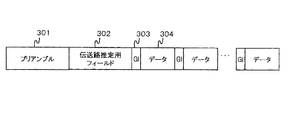
図3は、受信装置が受信する送信信号のフレームフォーマットの一例を表す説明図である。送信信号のフレームフォーマットは、プリアンブル301、伝送路推定用フィールド302、ガードインターバル(GI)303、及びデータ304を含む構成である。
FIG. 3 is an explanatory diagram illustrating an example of a frame format of a transmission signal received by the receiving apparatus. The frame format of the transmission signal includes a
プリアンブル301は、既知の信号波形を複数回繰り返した信号波形を含む。例えば、プリアンブル301には、相関特性に優れる128ビットのGolay系列をBPSK変調した信号波形を一単位として、一単位とした信号波形を複数回繰り返した波形が用いられる。受信装置は、受信した既知の信号波形の繰り返しを相関検出により求め、たとえば、フレームの検出、ゲイン制御、キャリア周波数同期の少なくとも1つ以上に用いる。
The
伝送路推定用フィールド302は、同様に複数個の既知の信号波形を含み、本発明に係る受信装置において伝送路の歪み推定に用いられる。例えば、伝送路推定用フィールド302には、128bitのGolay系列と128bitのGolay系列の相補系列をBPSK変調した信号波形が用いられる。
Similarly, the transmission
ガードインターバル303は、データ304の区切りとして挿入されている。ガードインターバル303にも、同様に既知の信号波形、例えば64bitのGolay系列をBPSK変調した信号が用いられる。
The
データ304は、ブロック単位によって誤り訂正符号化されたデータビット列をPSK又はQAM変調したシンボル列を含む構成である。
The
上述したフレームフォーマット(信号フォーマット)を用いてデジタル変調された送信信号のシンボル列は、送信帯域制限フィルタとしてルートレイズドコサインフィルタに掛けられ、DAコンバータによりアナログベースバンド信号に変換される。ベースバンド信号は、RF部においてシングルキャリア高周波信号に変換され、アンテナから送信される。 The symbol sequence of the transmission signal digitally modulated using the frame format (signal format) described above is subjected to a root raised cosine filter as a transmission band limiting filter and converted to an analog baseband signal by a DA converter. The baseband signal is converted into a single carrier high frequency signal in the RF unit and transmitted from the antenna.
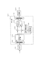
図2は、本発明に係る受信装置10の全体構成を表すブロック図である。受信装置10は、アンテナ201、RF部202、ADC(ADコンバータ)101、同期部204、等化部102及び復調部103を含む構成である。
FIG. 2 is a block diagram showing the overall configuration of the
RF部202は、アンテナ201により受信されたシングルキャリア高周波信号をダウンコンバートし、ベースバンド信号に変換する。ADコンバータ101は、ベースバンド信号をサンプリングし、デジタル信号に変換する。
The
同期部204は、デジタル信号に変換された受信信号のプリアンブル301を用いて、フレームの検出、RF部202のゲイン調整、キャリア周波数同期のうち少なくとも1つ以上の同期処理を行う。
The
等化部102は、同期部204において検出されたフレームタイミングに従い、伝送路推定用フィールド302を用いて伝送路の歪みを推定する。更に、等化部102は、図3に表す伝送路推定用フィールド302以降のデータ304における伝送路歪特性及びサンプリング位相誤差特性を補正し、シンボル列を出力する。
The
復調部103は、等化部102により出力されたシンボル列を入力し、信号点を判定してデータ復調し、送信データを再生する。
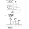
図1は、等化部102の内部構成を表すブロック図である。等化部102は、シリアル/パラレル(直並列)変換部104、PNポイントフーリエ変換部(FFT部)105、歪推定部106、補正係数算出部107及び補正係数乗算部(補正部)108、Nポイント逆フーリエ変換部(IFFT部)109及びパラレル/シリアル(並直列)変換部110を含む構成である。
FIG. 1 is a block diagram showing the internal configuration of the
ADコンバータ101は、シンボル速度に対してP倍(P>1)の速度によって受信信号をオーバーサンプリングし、AD変換する。
The
シリアル/パラレル変換部104は、P倍オーバーサンプリングされたサンプル列から、補正の対象とするNシンボルに相当するP×N個のサンプルポイントを選択し、パラレル信号に変換する。
The serial /
PNポイントFFT部105は、パラレル信号に変換されたP×N個のサンプルポイントの信号をフーリエ変換し、周波数領域(受信信号帯域)毎のP×Nポイントの信号(周波数bin毎の複素ベクトル)に変換する。このうち、信号帯域に相当するNポイントの周波数領域信号が出力される。
The PN
歪推定部106は、伝送路推定用フィールド302が入力されている場合に、伝送路の歪みを推定する。具体的には、歪推定部106は、FFT部105から出力された伝送路推定用フィールド302のNポイントの周波数領域信号と、予め保持しておいた伝送路推定用フィールド302の送信波形をNポイントフーリエ変換した周波数領域信号(第1リファレンス信号)との差分ベクトルを周波数bin毎に求める。なお、差分ベクトルは、伝送路歪み特性に相当する。
The
補正係数算出部107は、歪推定部106により推定された伝送路歪み特性を基に、歪特性の逆特性となる様な補正ベクトルを求める。更に、補正係数算出部107は、受信帯域制限フィルタとしてルートレイズドコサインフィルタの周波数領域特性(受信フィルタ特性)を予め求めておき、周波数bin毎に、補正ベクトルに重み付けをしても良い。
The correction
歪推定部106は、ガードインターバル(GI)303が入力されている場合に、FFT部105から出力されたGI303のNポイントの周波数領域信号と、予め保持しておいたGI303の送信波形をNポイントフーリエ変換した周波数領域信号(第2リファレンス信号)との差分ベクトルを周波数bin毎に求める。なお、差分ベクトルがサンプリング位相ずれ特性(位相誤差特性)に相当する。
When the guard interval (GI) 303 is input, the
なお、差分ベクトル、即ち位相誤差特性を求める場合、伝送路推定用フィールド302において推定した伝送路歪み特性を補正しても良い。或いは、歪推定部106は、サンプリング位相ずれに相当する周波数bin毎の位相誤差を求め、補正係数算出部107は、位相誤差の逆特性となる様な位相補正を、前述した補正ベクトルに乗算しても良い。
When obtaining the difference vector, that is, the phase error characteristic, the transmission path distortion characteristic estimated in the transmission
補正係数乗算部108は、データ304が入力されている場合に、FFT部105から出力されたNポイントの周波数領域信号に対し、周波数bin毎に補正係数算出部107により出力された補正ベクトルを乗算し、歪み補正する。
The correction
Nポイント逆フーリエ変換(IFFT)部109は、補正係数乗算部108により歪み補正したNポイントの周波数領域信号を逆フーリエ変換し、N個のサンプルポイントの時間領域信号に変換する。歪み補正したNポイントの周波数領域信号は、シンボル速度と同じサンプリング速度の時間領域信号に変換される。
An N-point inverse Fourier transform (IFFT)
パラレル/シリアル変換部110は、N個のサンプルポイント(=Nシンボル)の時間領域信号をシリアル信号に変換する。パラレル/シリアル変換部110は、N個のサンプルポイントのうち、FFT及びIFFTの波形打ち切りの影響をうける先頭及び最後の数サンプルを除去した中央の部分サンプル列、例えば中央のN/2個のサンプルポイントのサンプル列を出力する。 The parallel / serial converter 110 converts a time domain signal of N sample points (= N symbols) into a serial signal. The parallel / serial conversion unit 110 removes the first and last few samples affected by the FFT and IFFT waveform truncation from among the N sample points, for example, the central N / 2 samples. Output a sample sequence of points.
等化部102に入力されたサンプル列から補正の対象とするNシンボル(N個のサンプルポイント)を、N/2シンボルずつオーバーラップさせながら、等化部102に入力するため、等化部102から出力されるサンプル列の連続性が保たれる。
In order to input N symbols (N sample points) to be corrected from the sample sequence input to the
図4は、補正の対象とする信号の処理単位の一例を表す説明図である。図4では、シンボル速度に対してP=2倍の速度においてオーバーサンプリングしたサンプル列401が入力されている。また、補正対象の処理単位をN=64シンボルとする。
FIG. 4 is an explanatory diagram illustrating an example of a processing unit of a signal to be corrected. In FIG. 4, a
シリアル/パラレル変換部104は、サンプル列401から64シンボル分に相当する128個のサンプルポイントのサンプル列402−1を選択する。シリアル/パラレル変換部104は、N/2=32シンボル(N=64)ずつオーバーラップさせたサンプル列402(402−1,402−2,402−2)を処理単位として選択する。
The serial /
等化部102は、選択されたサンプル列402−1を、128ポイントフーリエ変換及び歪み補正し、64ポイント逆フーリエ変換により64シンボル(64個のサンプルポイント)の時間領域信号403に変換する。
The
時間領域信号403から、中央部分の32シンボル(32個のサンプルポイント)分のサンプル列404−1が選択されて出力される。サンプル列402−2、402−3も同様に処理され、サンプル列404−2,404−3(部分時系列)に変換される。
From the
これらのサンプル列402−1,402−2,402−2が連結されると、シンボル速度とサンプル速度が等しい等倍サンプリングのサンプル(シンボル)列405は、連続性が保たれたまま出力される。
When these sample sequences 402-1, 402-2, and 402-2 are connected, a sample (symbol)
次に、等化部102における歪み補正について説明する。
Next, distortion correction in the
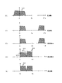
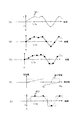
図5は、等化部102の内部の信号をスペクトルによって表現したグラフである。図5(A)〜図5(E)において、横軸は周波数若しくは周波数binを表し、縦軸は信号の強さを表す。
FIG. 5 is a graph representing the signal inside the
図5(A)は、ADコンバータ101に入力されたアナログベースバンド信号のスペクトル501を表す。ここで、ベースバンド信号は複素信号であり、シンボル速度をfs(Hz)とする。入力信号であるアナログベースバンド信号のスペクトル501は、DC成分(0Hz)を中心に帯域幅fs(Hz)のスペクトルとなる。
FIG. 5A shows a
図5(B)は、入力信号をADコンバータ101においてP=2倍のオーバーサンプリングした後の信号のスペクトルを表す。サンプリング速度が2fs(Hz)であるので、fs(Hz)を中心に折り返し(エイリアシング)が生じる。
FIG. 5B shows a spectrum of the signal after the input signal is oversampled by P = 2 times in the
図5(C)は、サンプル列を128ポイントFFTにおいて周波数領域信号に変換した信号のスペクトルを表す。横軸は、2fs(Hz)を128ポイントに離散化した周波数bin(k=0から127)となる。信号帯域は、k=0〜31の周波数binと、96〜127の周波数binに存在する。 FIG. 5C shows a spectrum of a signal obtained by converting a sample sequence into a frequency domain signal by 128-point FFT. The horizontal axis represents the frequency bin (k = 0 to 127) obtained by discretizing 2 fs (Hz) into 128 points. The signal band exists at a frequency bin of k = 0 to 31 and a frequency bin of 96 to 127.
図5(D)は、128ポイントFFTにより周波数領域信号に変換した信号のスペクトルから信号帯域に相当する64ポイント分の周波数binを取り出した信号のスペクトルを表す。前述した様に、信号の周波数特性501aと、リファレンス信号の周波数特性502(点線)との差分が歪推定部106において求められ、差分を補正する補正係数503が補正係数算出部107により求められる。
FIG. 5D shows a spectrum of a signal obtained by extracting 64 points of frequency bin corresponding to the signal band from the spectrum of the signal converted into the frequency domain signal by 128-point FFT. As described above, the difference between the frequency characteristic 501a of the signal and the frequency characteristic 502 (dotted line) of the reference signal is obtained by the
補正係数503を信号の各周波数binに乗算した結果、図5(E)に表す様に、歪みが補正されたスペクトル504が得られる。スペクトル504を64ポイントIFFTにおいて時間軸信号に変換され、等化後の信号として出力される。
As a result of multiplying each frequency bin of the signal by the correction coefficient 503, a
ここで、数式を用いて歪み補正について説明する。 Here, distortion correction will be described using mathematical expressions.
送信信号をx(t)、受信信号をr(t)、送信装置と受信装置との間の伝送路特性をh(t)とする。x(t)、r(t)、h(t)をフーリエ変換した値をそれぞれX(f)、R(f)、H(f)とすると、数式(1)が得られる。 It is assumed that the transmission signal is x (t), the reception signal is r (t), and the transmission path characteristic between the transmission device and the reception device is h (t). When values obtained by Fourier transforming x (t), r (t), and h (t) are X (f), R (f), and H (f), respectively, Equation (1) is obtained.
![]()
![]()
伝送路推定シンボルをx_ref(t)、伝送路推定シンボルをフーリエ変換した値をX_ref(f)、受信した伝送路推定シンボルをr_ref(t)、受信した伝送路推定シンボルをフーリエ変換した値をR_ref(f)とすると、伝送路特性H(f)は数式(2)によって求まる。なお、伝送路推定シンボルのフーリエ変換した値R_ref(f)は、リファレンス信号の周波数特性502(図5(D)参照)に相当する。
The transmission path estimation symbol is x_ref (t), the transmission path estimation symbol is Fourier transformed to X_ref (f), the received transmission path estimation symbol is r_ref (t), and the received transmission path estimation symbol is Fourier transformed to R_ref. Assuming (f), the transmission line characteristic H (f) is obtained by the equation (2). A value R_ref (f) obtained by Fourier transform of the transmission path estimation symbol corresponds to the
![]()
![]()
送信したデータシンボルをx_data(t)、送信したデータシンボルをフーリエ変換した値をX_data(f)、受信したデータシンボルをr_data(t)、受信したデータシンボルをフーリエ変換した値をR_data(f)とすると、数式(3)が得られる。 The transmitted data symbol is x_data (t), the value obtained by Fourier transforming the transmitted data symbol is X_data (f), the received data symbol is r_data (t), and the value obtained by Fourier transforming the received data symbol is R_data (f). Then, Formula (3) is obtained.

ここで、伝送路推定シンボルによって推定された伝送路特性H(f)と、データシンボル受信時点の伝送路特性H’(f)とが等しいとすれば、数式(4)に従って、受信装置10は、送信データシンボルを再生できる。即ち、再生した送信データシンボルX’_data(f)は、受信したデータシンボルをフーリエ変換した値R_data(f)に、補正係数1/H(f)を乗算することにより得られる。なお、補正係数1/H(f)は補正係数503(図5(D)参照)に相当する。
Here, assuming that the transmission path characteristic H (f) estimated by the transmission path estimation symbol is equal to the transmission path characteristic H ′ (f) at the time of receiving the data symbol, the receiving
![]()
![]()
次に、等化部102におけるサンプリングタイミングずれ補正について説明する。
Next, the sampling timing deviation correction in the
図6は、等化部102の内部の信号を表すグラフである。図6(A)〜(E)のうち図6(D)を除き、横軸は時間軸を表し、縦軸は信号の強さを表す。図6(D)においては、横軸は周波数を表し、縦軸は位相差を表す。
FIG. 6 is a graph showing signals inside the
図6には、送信の信号点601、及び等化部102によって再生された信号点602が表されている。また、送信の信号点601は、シンボル速度fs(Hz)、即ちシンボル間隔1/fs(sec)によってBPSK変調されている。
FIG. 6 shows a transmission signal point 601 and a signal point 602 reproduced by the
送信時に帯域制限フィルタ(例えば、ルートレイズドコサインフィルタ)により帯域が制限され、送信信号は、図6(A)の実線に示すアナログベースバンド信号波形として送信される。 At the time of transmission, the band is limited by a band limiting filter (for example, a root raised cosine filter), and the transmission signal is transmitted as an analog baseband signal waveform indicated by a solid line in FIG.
図6(B)は、入力信号(点線)をADコンバータ101がP=2倍のオーバーサンプリングタイミングによって(つまり、1/2fsごとに)サンプリングしたサンプル列(黒点)を表す。図6(B)では、送信信号点のタイミング(シンボルタイミング)とサンプリングタイミングが一致している場合が示される。
FIG. 6B shows a sample string (black dot) in which the input signal (dotted line) is sampled by the
一方、図6(C)には、サンプリングタイミングの位相がシンボルタイミングとずれている場合が示されている。 On the other hand, FIG. 6C shows a case where the phase of the sampling timing is shifted from the symbol timing.
図6(B)及び図6(C)において、サンプリングされた信号を周波数領域に変換し、周波数bin毎の位相差を検出すると、図6(D)に表す様に、サンプリング位相差は、周波数に比例した位相回転として検出できる。 In FIG. 6B and FIG. 6C, when the sampled signal is converted into the frequency domain and the phase difference for each frequency bin is detected, as shown in FIG. It can be detected as a phase rotation proportional to.
例えば、補正係数算出部107は、レファレンス信号(図5(B)参照)の周波数bin毎の複素ベクトルの位相を基準とし、既知信号であるガードインターバル303の信号を歪み補正した場合の周波数bin毎の残留位相誤差を直線近似する(図6(D)参照)。
For example, the correction
補正係数算出部107は、残留位相誤差を打ち消すために、逆回転を掛ける様に補正することにより、時間領域信号に変換した場合のサンプリングタイミングをシンボルタイミングに合わせることができる(図6(E)参照)。
The correction
図6(E)では、図6(C)に示す入力信号に対し、周波数領域において図6(D)に表す様な位相回転を補正してから時間領域信号に変換することにより、シンボルタイミング(1/fs間隔)に送信信号点が再生されている(再生した信号点602参照)。再生した信号を復調部103において判定することによって、図6(E)の実線によって示す受信ビット列が得られる。
In FIG. 6E, the input signal shown in FIG. 6C is corrected to the phase rotation as shown in FIG. 6D in the frequency domain and then converted into a time domain signal, so that the symbol timing ( Transmission signal points are reproduced at 1 / fs intervals (see reproduced signal points 602). By determining the reproduced signal in the
ここで、数式を用いてサンプリングタイミングすれ補正について説明する。 Here, the sampling timing deviation correction will be described using mathematical expressions.
送受信間のサンプリングクロック周波数ずれがあると、受信装置10においてフーリエ変換の対象とする切り出しブロック期間が送信信号に対して徐々にずれていく。図7は、送受信間のサンプリング周波数ずれによる切り出しブロックのタイミングずれを表すタイミングチャートである。
When there is a sampling clock frequency shift between transmission and reception, the cut-out block period to be subjected to Fourier transform in the receiving
図7(A)はサンプリング周波数ずれが無い場合を示し、図7(B)はサンプリング周波数ずれがある場合を示す。サンプリング周波数のずれとして、切り出しブロックのタイミングずれΔtが生じている。 FIG. 7A shows a case where there is no sampling frequency deviation, and FIG. 7B shows a case where there is a sampling frequency deviation. As a sampling frequency shift, a cut-off block timing shift Δt occurs.
図6(B)、(C)に表す様に、ブロック内においてサンプル位相がずれることにより、周波数領域に変換された信号には、図6(D)に示す様に、周波数binに比例する位相回転が生じる。 As shown in FIGS. 6B and 6C, the signal converted into the frequency domain due to the shift of the sample phase in the block has a phase proportional to the frequency bin as shown in FIG. 6D. Rotation occurs.
位相回転が生じた受信信号をフーリエ変換した値R’(f)は、数式(5)によって表される。ここで、パラメータNは、FFTポイント数(ブロックのサンプル数)を表す。パラメータfは、周波数binを表す。パラメータΔtは、切り出しブロックのタイミングずれを表す。 A value R ′ (f) obtained by performing Fourier transform on the received signal in which the phase rotation has occurred is expressed by Equation (5). Here, the parameter N represents the number of FFT points (number of block samples). The parameter f represents the frequency bin. The parameter Δt represents the timing shift of the cut block.
![]()
![]()
伝送路推定シンボルの切り出しとデータシンボルの切り出しとにおいて、送信信号に対して切り出しブロックのタイミングずれΔtが生じることにより、次の様な事象が起こる。 In the extraction of the transmission path estimation symbol and the extraction of the data symbol, the following phenomenon occurs due to the occurrence of the timing difference Δt of the extracted block with respect to the transmission signal.
具体的には、前述したデータシンボルの受信信号をフーリエ変換した値R’_data(f)を、伝送路推定シンボルによって推定された伝送路特性H(f)によって除算して周波数領域等化しても、数式(6)に表す様に、切り出しブロックのタイミングずれΔtに起因する各周波数における位相回転の項が残る。 Specifically, the value R′_data (f) obtained by Fourier-transforming the received signal of the data symbol described above may be divided by the transmission path characteristic H (f) estimated by the transmission path estimation symbol to equalize the frequency domain. As expressed in Equation (6), there remains a phase rotation term at each frequency due to the timing shift Δt of the cut-out block.
ここで、データ部分に既知系列として挿入されているガードインターバル303をx_gi(t)とし、ガードインターバル303をフーリエ変換した値をX_gi(f)とする。ガードインターバル303については、伝送路特性H(f)及びXgi(f)によって除算することにより、数式(7)に表す様に、切り出しブロックのタイミングずれΔtに起因する位相回転θ(f)を推定できる。
Here, the
よって、補正係数算出部107は、位相回転θ(f)をキャンセルするような逆特性1/θ(f)を数式(8)に表す様に求めることができる。
Therefore, the correction
これにより、伝送路特性H(f)を補正すると、タイミングずれΔtが補正された伝送路特性H’’(f)は、数式(9)により表される。 As a result, when the transmission line characteristic H (f) is corrected, the transmission line characteristic H ″ (f) in which the timing shift Δt is corrected is expressed by Expression (9).
これ以降のデータシンボルは、補正された伝送路特性H’’(f)によって等化されるため、等化器102は、送信データシンボルを再生できる。再生したデータシンボルは、数式(10)により表される。
Since the subsequent data symbols are equalized by the corrected transmission line characteristic H ″ (f), the
本実施形態の受信装置によれば、Nシンボルに相当するブロック単位において周波数領域に変換し、伝送路の歪み特性及びサンプリング位相誤差を補正するので、回路規模を増大せずに、シンボルタイミングずれ及び歪み補正できる。 According to the receiving apparatus of the present embodiment, conversion to the frequency domain is performed in units of blocks corresponding to N symbols, and distortion characteristics and sampling phase errors of the transmission path are corrected. Can correct distortion.
従って、サンプル毎の高速演算が求められる時間領域におけるシンボル同期を用いなくても、つまり、シンボル速度が高速であるため、時間領域処理によるシンボル同期が困難な場合でも、シンボルタイミングずれを補償できる。 Therefore, even if symbol synchronization in the time domain where high speed calculation is required for each sample is not used, that is, since symbol speed is high, symbol timing deviation can be compensated even if symbol synchronization by time domain processing is difficult.
以上、図面を参照しながら各種の実施形態について説明したが、本発明はかかる例に限定されないことは言うまでもない。当業者であれば、特許請求の範囲に記載された範疇内において、各種の変更例または修正例に想到し得ることは明らかであり、それらについても当然に本発明の技術的範囲に属すると了解される。 While various embodiments have been described above with reference to the drawings, it goes without saying that the present invention is not limited to such examples. It will be apparent to those skilled in the art that various changes and modifications can be made within the scope of the claims, and these are naturally within the technical scope of the present invention. Is done.
なお、実施の形態にかかる各構成は、集積回路であるLSIとして実現されてもよい。この場合、1チップ化されてもよいし、一部または全てを含むように1チップ化されてもよい。ここでは、LSIと称したが、集積度の違いによっては、IC、システムLSI、スーパーLSI、ウルトラLSIと称呼されることもある。 Each configuration according to the embodiment may be realized as an LSI which is an integrated circuit. In this case, it may be made into one chip, or it may be made into one chip so as to include a part or all of it. Although referred to here as LSI, depending on the degree of integration, it may be referred to as IC, system LSI, super LSI, or ultra LSI.
また、集積回路化の手法は、LSIに限られず、専用回路または汎用プロセッサにより集積回路化してもよい。また、LSI製造後にプログラムできるFPGA(Field-Programmable Gate Array)又は、LSI内部の回路セルの接続、設定を再構成可能なリコンフィギュラブル・プロセッサを用いてもよい。 Further, the method of circuit integration is not limited to LSI, and circuit integration may be performed with a dedicated circuit or a general-purpose processor. Alternatively, a field-programmable gate array (FPGA) that can be programmed after manufacturing the LSI or a reconfigurable processor that can reconfigure the connection and setting of circuit cells inside the LSI may be used.
また、これらの機能ブロックの演算は、例えばDSP、CPUを用いて演算できる。さらに、これらの処理ステップはプログラムとして記録媒体に記録して実行できる。 Moreover, the calculation of these functional blocks can be calculated using, for example, a DSP or a CPU. Further, these processing steps can be recorded on a recording medium as a program and executed.
さらには、半導体技術の進歩または派生する別技術によりLSIに置き換わる集積回路化の技術が登場すれば、当然、その別技術を用いて機能ブロックを集積化してもよい。 Furthermore, if integrated circuit technology comes out to replace LSI's as a result of the advancement of semiconductor technology or a derivative other technology, it is naturally also possible to integrate function blocks using this other technology.
本発明は、シングルキャリア伝送方式に用いる周波数領域等化器(等化部)を有する受信装置として、小回路規模・低消費電力が要求されるモバイル通信を含む無線通信機器全般に広く適用できる。 INDUSTRIAL APPLICABILITY The present invention can be widely applied to radio communication equipment in general including mobile communication that requires a small circuit scale and low power consumption as a receiving apparatus having a frequency domain equalizer (equalization unit) used for a single carrier transmission system.
10 受信装置
101 ADコンバータ
102 等化部
103 復調部
104 シリアル/パラレル変換部
105 PNポイントフーリエ変換部(FFT部)
106 歪推定部
107 補正係数算出部
108 補正係数乗算部
109 Nポイント逆フーリエ変換部(IFFT部)
110 パラレル/シリアル変換部
201 アンテナ
202 RF部
204 同期部
301 プリアンブル
302 伝送路推定用フィールド
303 ガードインターバル
304 データ
401、402−1、402−2、402−3 サンプル列
403 時間軸信号
404−1、404−2、404−3、405 サンプル列
501 ベースバンド信号のスペクトル
501a 信号の周波数特性
502 リファレンス信号の周波数特性
503 補正係数
504 歪みが補正されたスペクトル
601 送信の信号点
602 再生された信号点
DESCRIPTION OF
106
DESCRIPTION OF SYMBOLS 110 Parallel /
Claims (4)
受信信号をシンボル速度に対してP倍(Pは1以上の整数)の速度によってオーバーサンプリングするADコンバータと、
前記ADコンバータの出力から、Nシンボルに相当するP×N個のサンプルポイントの時間領域信号を選択し、前記P×Nポイントの時間領域信号をフーリエ変換してP×Nポイントの周波数領域信号に変換し、前記P×Nポイントの周波数領域信号のうち、受信信号帯域に相当するNポイントの周波数領域信号を出力するフーリエ変換部と、
前記フーリエ変換部から出力されるNポイントの周波数領域信号のうち、補正係数を算出するための第1のNポイントの周波数領域信号と、前記受信装置が既知のリファレンス信号の周波数領域信号との差分から歪特性又は位相誤差特性を推定する歪推定部と、
前記歪特性又は位相誤差特性を補正するための補正係数を算出する補正係数算出部と、
前記フーリエ変換部から出力される周波数領域信号のうち、歪特性又は位相誤差特性の補正対象である第2のNポイントの周波数領域信号に、前記補正係数を乗算して、前記第2のNポイントの周波数領域信号を補正する補正部と、
前記補正された第2のNポイントの周波数領域信号を逆フーリエ変換して前記シンボル速度と同じサンプリング速度のNポイントの時間領域信号に変換し、Nサンプルの時間領域信号から部分時系列を出力する逆フーリエ変換部と、
を備える受信装置。 A receiving device for receiving a transmission signal modulated using a single carrier transmission method,
An AD converter that oversamples the received signal at a rate P times the symbol rate (P is an integer of 1 or more);
From the output of the AD converter, a time domain signal of P × N sample points corresponding to N symbols is selected, and the time domain signal of P × N points is Fourier transformed into a frequency domain signal of P × N points. A Fourier transform unit that converts and outputs an N-point frequency domain signal corresponding to a received signal band among the P × N-point frequency domain signals;
Of the N-point frequency domain signals output from the Fourier transform unit, the difference between the first N-point frequency domain signal for calculating the correction coefficient and the frequency domain signal of the reference signal known by the receiver A distortion estimator for estimating distortion characteristics or phase error characteristics from:
A correction coefficient calculation unit for calculating a correction coefficient for correcting the distortion characteristic or the phase error characteristic;
Of the frequency domain signals output from the Fourier transform unit, a second N point frequency domain signal that is a correction target of distortion characteristics or phase error characteristics is multiplied by the correction coefficient to obtain the second N points. A correction unit for correcting the frequency domain signal of
The corrected second N-point frequency domain signal is inverse Fourier transformed to be converted into an N-point time domain signal having the same sampling rate as the symbol rate, and a partial time series is output from the N-sample time domain signal. An inverse Fourier transform unit;
A receiving device.
前記補正係数算出部は、前記歪特性の逆特性又は前記位相誤差特性に加え、受信フィルタ特性を補正するための補正係数を算出する受信装置。 The receiving device according to claim 1,
The correction coefficient calculation unit is a reception device that calculates a correction coefficient for correcting a reception filter characteristic in addition to the inverse characteristic of the distortion characteristic or the phase error characteristic.
前記送信信号は、プリアンブル、伝送路推定用フィールド、ガードインターバルおよびデータを含む信号フォーマットを有し、
前記フーリエ変換部は、
前記伝送路推定用フィールド、又は、前記ガードインターバルを用いて、前記第1のNポイントの周波数領域信号を出力し、前記データを用いて前記第2のNポイントの周波数領域信号を出力し、
前記歪推定部は、前記伝送路推定用フィールドの周波数領域信号を用いて前記歪特性を推定し、前記ガードインターバルの周波数領域信号を用いて前記位相誤差特性を推定する
受信装置。 The receiving device according to claim 1,
The transmission signal has a signal format including a preamble, a transmission path estimation field, a guard interval, and data,
The Fourier transform unit
The first N-point frequency domain signal is output using the transmission path estimation field or the guard interval, and the second N-point frequency domain signal is output using the data.
The distortion estimation unit estimates the distortion characteristics using a frequency domain signal of the transmission path estimation field, and estimates the phase error characteristics using a frequency domain signal of the guard interval.
前記第リファレンス信号は、予め保持しておいた前記伝送路推定用フィールド、又は、前記ガードインターバルをNポイントの周波数領域に変換した信号である受信装置。 The receiving device according to claim 1,
The receiving apparatus, wherein the first reference signal is a signal obtained by converting the transmission path estimation field stored in advance or the guard interval into an N-point frequency domain.
Priority Applications (3)
| Application Number | Priority Date | Filing Date | Title |
|---|---|---|---|
| JP2011073446A JP5707202B2 (en) | 2011-03-29 | 2011-03-29 | Receiver |
| PCT/JP2012/000800 WO2012132191A1 (en) | 2011-03-29 | 2012-02-07 | Reception device |
| US13/814,902 US9191046B2 (en) | 2011-03-29 | 2012-02-07 | Reception device |
Applications Claiming Priority (1)
| Application Number | Priority Date | Filing Date | Title |
|---|---|---|---|
| JP2011073446A JP5707202B2 (en) | 2011-03-29 | 2011-03-29 | Receiver |
Publications (3)
| Publication Number | Publication Date |
|---|---|
| JP2012209736A true JP2012209736A (en) | 2012-10-25 |
| JP2012209736A5 JP2012209736A5 (en) | 2013-09-19 |
| JP5707202B2 JP5707202B2 (en) | 2015-04-22 |
Family
ID=46929988
Family Applications (1)
| Application Number | Title | Priority Date | Filing Date |
|---|---|---|---|
| JP2011073446A Expired - Fee Related JP5707202B2 (en) | 2011-03-29 | 2011-03-29 | Receiver |
Country Status (3)
| Country | Link |
|---|---|
| US (1) | US9191046B2 (en) |
| JP (1) | JP5707202B2 (en) |
| WO (1) | WO2012132191A1 (en) |
Cited By (1)
| Publication number | Priority date | Publication date | Assignee | Title |
|---|---|---|---|---|
| JP2014155214A (en) * | 2013-02-14 | 2014-08-25 | National Institute Of Information & Communication Technology | Golay code sequence correlator and equalizer using the same |
Families Citing this family (6)
| Publication number | Priority date | Publication date | Assignee | Title |
|---|---|---|---|---|
| GB2514595B (en) * | 2013-05-30 | 2017-10-18 | Imp Innovations Ltd | Method and apparatus for estimating frequency domain representation of signals |
| US9166776B2 (en) * | 2013-10-04 | 2015-10-20 | Amlogic Co., Ltd. | Methods and systems for optimal PN phase detection in DTMB receivers |
| US10341157B2 (en) | 2014-12-29 | 2019-07-02 | Telefonaktiebolaget Lm Ericsson (Publ) | Method for symbol compensation and receiver |
| WO2017131457A1 (en) * | 2016-01-27 | 2017-08-03 | Samsung Electronics Co., Ltd. | Method and apparatus for estimating and correcting phase error in wireless communication system |
| KR102529191B1 (en) * | 2016-01-27 | 2023-05-08 | 삼성전자주식회사 | Method and apparatus for estmating and correcting phase error in a wireless communication system |
| CN108234374B (en) * | 2016-12-14 | 2020-09-25 | 联芯科技有限公司 | Uplink multi-carrier transmitting device, system and method |
Citations (5)
| Publication number | Priority date | Publication date | Assignee | Title |
|---|---|---|---|---|
| JP2006245810A (en) * | 2005-03-01 | 2006-09-14 | Sumitomo Electric Ind Ltd | Fraction spacing equalizer and receiver using it |
| WO2007015317A1 (en) * | 2005-08-02 | 2007-02-08 | Sumitomo Electric Industries, Ltd. | Transmitter, receiver, communication method and transmitting/receiving system |
| JP4271235B2 (en) * | 2004-07-16 | 2009-06-03 | 富士通株式会社 | Method and apparatus for frequency domain equalization in a single carrier receiver |
| JP4635750B2 (en) * | 2005-07-07 | 2011-02-23 | 日本電気株式会社 | Equalizer and equalization method |
| JP2012120134A (en) * | 2010-12-03 | 2012-06-21 | Osaka Prefecture Univ | Transmission/reception method |
Family Cites Families (4)
| Publication number | Priority date | Publication date | Assignee | Title |
|---|---|---|---|---|
| JP3090138B2 (en) * | 1999-02-04 | 2000-09-18 | 日本電気株式会社 | Receiving machine |
| US6834079B1 (en) * | 2000-10-20 | 2004-12-21 | 3Com Corporation | Efficient implementation for equalization of multicarrier channels |
| US20030200243A1 (en) * | 2002-04-19 | 2003-10-23 | Matsushita Electric Industrial Co., Ltd. | Finite impulse response filter, communication transmission apparatus and communication reception apparatus |
| JPWO2006006238A1 (en) * | 2004-07-14 | 2008-04-24 | 富士通株式会社 | Multi-carrier receiving method and multi-carrier receiving apparatus |
-
2011
- 2011-03-29 JP JP2011073446A patent/JP5707202B2/en not_active Expired - Fee Related
-
2012
- 2012-02-07 US US13/814,902 patent/US9191046B2/en not_active Expired - Fee Related
- 2012-02-07 WO PCT/JP2012/000800 patent/WO2012132191A1/en active Application Filing
Patent Citations (5)
| Publication number | Priority date | Publication date | Assignee | Title |
|---|---|---|---|---|
| JP4271235B2 (en) * | 2004-07-16 | 2009-06-03 | 富士通株式会社 | Method and apparatus for frequency domain equalization in a single carrier receiver |
| JP2006245810A (en) * | 2005-03-01 | 2006-09-14 | Sumitomo Electric Ind Ltd | Fraction spacing equalizer and receiver using it |
| JP4635750B2 (en) * | 2005-07-07 | 2011-02-23 | 日本電気株式会社 | Equalizer and equalization method |
| WO2007015317A1 (en) * | 2005-08-02 | 2007-02-08 | Sumitomo Electric Industries, Ltd. | Transmitter, receiver, communication method and transmitting/receiving system |
| JP2012120134A (en) * | 2010-12-03 | 2012-06-21 | Osaka Prefecture Univ | Transmission/reception method |
Non-Patent Citations (4)
| Title |
|---|
| JPN6015003726; 小原辰徳、武田一樹、安達文幸: 'シングルキャリア伝送におけるOverlap FDEとブロック間干渉キャンセラの特性比較' 電子情報通信学会技術研究報告 Vol.110、No.433, 20110223, pp.25-29, 社団法人電子情報通信学会 * |
| JPN6015003728; 久万善広、梅比良正弘: 'オーバーラップFDEにおける短縮化CHU系列を用いたチャネル推定法の検討' 電子情報通信学会技術研究報告 Vol.108、No.188, 20080820, pp.7-12, 社団法人電子情報通信学会 * |
| JPN6015003730; 小原辰徳、武田一樹、安達文幸: '受信タイミングオフセットが存在する場合の周波数領域等化シングルキャリア伝送における時間多重パイロット' 電子情報通信学会技術研究報告 Vol.109、No.368, 20100114, pp.217-222, 社団法人電子情報通信学会 * |
| JPN6015003731; P.P.Vaidyanathan, Bojan Vrcelj: 'Theory of fractionally spaced cyclic-prefix equalizers' Acoustics, Speech, and Signal Processing (ICASSP), 2002 IEEE International Conference on Vol.2, 200205 * |
Cited By (1)
| Publication number | Priority date | Publication date | Assignee | Title |
|---|---|---|---|---|
| JP2014155214A (en) * | 2013-02-14 | 2014-08-25 | National Institute Of Information & Communication Technology | Golay code sequence correlator and equalizer using the same |
Also Published As
| Publication number | Publication date |
|---|---|
| US9191046B2 (en) | 2015-11-17 |
| JP5707202B2 (en) | 2015-04-22 |
| WO2012132191A1 (en) | 2012-10-04 |
| US20130136165A1 (en) | 2013-05-30 |
Similar Documents
| Publication | Publication Date | Title |
|---|---|---|
| JP5707202B2 (en) | Receiver | |
| KR100770924B1 (en) | Apparatus and method for compensating frequency offset in a wireless communication system | |
| US20160087830A1 (en) | Multi-Mode Orthogonal Frequency Division Multiplexing Transmitter for Highly-Spectrally-Efficient Communications | |
| JP3492565B2 (en) | OFDM communication device and detection method | |
| WO2014132599A1 (en) | Reception apparatus, phase error estimation method, and phase error correction method | |
| JP4654797B2 (en) | Equalizer and equalization method | |
| EP2192735A1 (en) | Receiving apparatus and method for receiving signals in a wireless communication system with improved equalization performance | |
| JP2010515403A (en) | Method and apparatus for reducing inter-carrier interference in an OFDM system | |
| JP2015198449A (en) | Method and device for cancelling narrow band interference in single carrier signal and computer program | |
| JP3910956B2 (en) | Propagation path estimator and receiving apparatus using the same for OFDM wireless communication system | |
| JP2007019805A (en) | Equalizer and equalizing method | |
| US20100074346A1 (en) | Channel estimation in ofdm receivers | |
| JP5624527B2 (en) | Single carrier receiver | |
| JP4190406B2 (en) | Frequency offset estimation method and frequency offset correction apparatus using the same | |
| JP2010124368A (en) | Doppler frequency estimating device, receiving device, program, and method of estimating doppler frequency | |
| JP5599353B2 (en) | Transceiver | |
| JP5871841B2 (en) | Carrier frequency offset correction method and apparatus | |
| JP6028572B2 (en) | Receiver | |
| JP5182699B2 (en) | Reception device, radio signal reception method, radio communication system, and program | |
| US20050073947A1 (en) | Channel estimator for a receiver and method of operation thereof | |
| EP2928139B1 (en) | Method and a device for cancelling a narrow band interference in a single carrier signal | |
| WO2023053472A1 (en) | Wireless communication device, system, method, and non-transitory computer-readable medium | |
| KR101275693B1 (en) | Method and apparatus of estimating frequency offset based on blind approach in wireless communication system | |
| JP2007235407A (en) | Adaptive equalizer and communication apparatus | |
| JP5089425B2 (en) | Communication device |
Legal Events
| Date | Code | Title | Description |
|---|---|---|---|
| A521 | Request for written amendment filed |
Free format text: JAPANESE INTERMEDIATE CODE: A523 Effective date: 20130801 |
|
| A621 | Written request for application examination |
Free format text: JAPANESE INTERMEDIATE CODE: A621 Effective date: 20130801 |
|
| RD04 | Notification of resignation of power of attorney |
Free format text: JAPANESE INTERMEDIATE CODE: A7424 Effective date: 20131225 |
|
| A131 | Notification of reasons for refusal |
Free format text: JAPANESE INTERMEDIATE CODE: A131 Effective date: 20140624 |
|
| A521 | Request for written amendment filed |
Free format text: JAPANESE INTERMEDIATE CODE: A523 Effective date: 20140819 |
|
| RD02 | Notification of acceptance of power of attorney |
Free format text: JAPANESE INTERMEDIATE CODE: A7422 Effective date: 20150116 |
|
| TRDD | Decision of grant or rejection written | ||
| A01 | Written decision to grant a patent or to grant a registration (utility model) |
Free format text: JAPANESE INTERMEDIATE CODE: A01 Effective date: 20150203 |
|
| A61 | First payment of annual fees (during grant procedure) |
Free format text: JAPANESE INTERMEDIATE CODE: A61 Effective date: 20150302 |
|
| R151 | Written notification of patent or utility model registration |
Ref document number: 5707202 Country of ref document: JP Free format text: JAPANESE INTERMEDIATE CODE: R151 |
|
| LAPS | Cancellation because of no payment of annual fees |