JP2012209464A - Organic electroluminescent element and manufacturing method for the same - Google Patents
Organic electroluminescent element and manufacturing method for the same Download PDFInfo
- Publication number
- JP2012209464A JP2012209464A JP2011074807A JP2011074807A JP2012209464A JP 2012209464 A JP2012209464 A JP 2012209464A JP 2011074807 A JP2011074807 A JP 2011074807A JP 2011074807 A JP2011074807 A JP 2011074807A JP 2012209464 A JP2012209464 A JP 2012209464A
- Authority
- JP
- Japan
- Prior art keywords
- layer
- organic
- light emitting
- injection layer
- electrode
- Prior art date
- Legal status (The legal status is an assumption and is not a legal conclusion. Google has not performed a legal analysis and makes no representation as to the accuracy of the status listed.)
- Withdrawn
Links
- 238000004519 manufacturing process Methods 0.000 title claims abstract description 22
- 238000002347 injection Methods 0.000 claims abstract description 119
- 239000007924 injection Substances 0.000 claims abstract description 119
- 238000005192 partition Methods 0.000 claims abstract description 73
- 239000000758 substrate Substances 0.000 claims abstract description 64
- 238000000034 method Methods 0.000 claims description 122
- 230000008569 process Effects 0.000 claims description 13
- 238000005401 electroluminescence Methods 0.000 claims description 7
- 230000007423 decrease Effects 0.000 claims description 4
- 229910052783 alkali metal Inorganic materials 0.000 claims description 3
- 150000001340 alkali metals Chemical class 0.000 claims description 3
- 150000001875 compounds Chemical class 0.000 claims description 3
- 239000000126 substance Substances 0.000 claims description 3
- 229910052784 alkaline earth metal Inorganic materials 0.000 claims description 2
- 150000001342 alkaline earth metals Chemical class 0.000 claims description 2
- 238000004020 luminiscence type Methods 0.000 claims 1
- 239000000243 solution Substances 0.000 abstract description 2
- 230000006866 deterioration Effects 0.000 abstract 1
- 239000010410 layer Substances 0.000 description 274
- 239000000463 material Substances 0.000 description 77
- 239000010408 film Substances 0.000 description 57
- 238000007639 printing Methods 0.000 description 23
- 239000011229 interlayer Substances 0.000 description 22
- 239000010409 thin film Substances 0.000 description 18
- 238000007740 vapor deposition Methods 0.000 description 16
- 229920005989 resin Polymers 0.000 description 15
- 239000011347 resin Substances 0.000 description 15
- 238000007789 sealing Methods 0.000 description 14
- YXFVVABEGXRONW-UHFFFAOYSA-N Toluene Chemical compound CC1=CC=CC=C1 YXFVVABEGXRONW-UHFFFAOYSA-N 0.000 description 12
- 230000015572 biosynthetic process Effects 0.000 description 12
- 238000000576 coating method Methods 0.000 description 11
- 230000000052 comparative effect Effects 0.000 description 11
- 239000011159 matrix material Substances 0.000 description 11
- 239000002904 solvent Substances 0.000 description 11
- 239000003566 sealing material Substances 0.000 description 10
- -1 tris (8-quinolinol) aluminum Chemical compound 0.000 description 10
- 238000004544 sputter deposition Methods 0.000 description 9
- 238000007774 anilox coating Methods 0.000 description 8
- 238000010438 heat treatment Methods 0.000 description 7
- 229910052751 metal Inorganic materials 0.000 description 7
- 239000002184 metal Substances 0.000 description 7
- 229910021417 amorphous silicon Inorganic materials 0.000 description 6
- 238000010586 diagram Methods 0.000 description 6
- 229910044991 metal oxide Inorganic materials 0.000 description 6
- 150000004706 metal oxides Chemical class 0.000 description 6
- 229920003227 poly(N-vinyl carbazole) Polymers 0.000 description 6
- 229910021420 polycrystalline silicon Inorganic materials 0.000 description 6
- 229920000642 polymer Polymers 0.000 description 6
- XLYOFNOQVPJJNP-UHFFFAOYSA-N water Substances O XLYOFNOQVPJJNP-UHFFFAOYSA-N 0.000 description 6
- 239000004840 adhesive resin Substances 0.000 description 5
- 229920006223 adhesive resin Polymers 0.000 description 5
- 229910052782 aluminium Inorganic materials 0.000 description 5
- XAGFODPZIPBFFR-UHFFFAOYSA-N aluminium Chemical compound [Al] XAGFODPZIPBFFR-UHFFFAOYSA-N 0.000 description 5
- 239000011521 glass Substances 0.000 description 5
- 230000005525 hole transport Effects 0.000 description 5
- 229910010272 inorganic material Inorganic materials 0.000 description 5
- 239000011147 inorganic material Substances 0.000 description 5
- 150000002500 ions Chemical class 0.000 description 5
- 238000010030 laminating Methods 0.000 description 5
- 238000004518 low pressure chemical vapour deposition Methods 0.000 description 5
- 229920005591 polysilicon Polymers 0.000 description 5
- 229920000178 Acrylic resin Polymers 0.000 description 4
- 239000004925 Acrylic resin Substances 0.000 description 4
- XUIMIQQOPSSXEZ-UHFFFAOYSA-N Silicon Chemical compound [Si] XUIMIQQOPSSXEZ-UHFFFAOYSA-N 0.000 description 4
- RDOXTESZEPMUJZ-UHFFFAOYSA-N anisole Chemical compound COC1=CC=CC=C1 RDOXTESZEPMUJZ-UHFFFAOYSA-N 0.000 description 4
- 239000010949 copper Substances 0.000 description 4
- 238000010894 electron beam technology Methods 0.000 description 4
- 239000007789 gas Substances 0.000 description 4
- 238000007733 ion plating Methods 0.000 description 4
- 229910052760 oxygen Inorganic materials 0.000 description 4
- 230000035699 permeability Effects 0.000 description 4
- 239000002985 plastic film Substances 0.000 description 4
- 229910052710 silicon Inorganic materials 0.000 description 4
- 239000010703 silicon Substances 0.000 description 4
- VYPSYNLAJGMNEJ-UHFFFAOYSA-N silicon dioxide Inorganic materials O=[Si]=O VYPSYNLAJGMNEJ-UHFFFAOYSA-N 0.000 description 4
- ZWEHNKRNPOVVGH-UHFFFAOYSA-N 2-Butanone Chemical compound CCC(C)=O ZWEHNKRNPOVVGH-UHFFFAOYSA-N 0.000 description 3
- CSCPPACGZOOCGX-UHFFFAOYSA-N Acetone Chemical compound CC(C)=O CSCPPACGZOOCGX-UHFFFAOYSA-N 0.000 description 3
- RYGMFSIKBFXOCR-UHFFFAOYSA-N Copper Chemical compound [Cu] RYGMFSIKBFXOCR-UHFFFAOYSA-N 0.000 description 3
- 229910052581 Si3N4 Inorganic materials 0.000 description 3
- 150000004982 aromatic amines Chemical class 0.000 description 3
- QVGXLLKOCUKJST-UHFFFAOYSA-N atomic oxygen Chemical compound [O] QVGXLLKOCUKJST-UHFFFAOYSA-N 0.000 description 3
- 239000011248 coating agent Substances 0.000 description 3
- 239000003086 colorant Substances 0.000 description 3
- 239000002131 composite material Substances 0.000 description 3
- 229910052802 copper Inorganic materials 0.000 description 3
- 238000001035 drying Methods 0.000 description 3
- 239000003822 epoxy resin Substances 0.000 description 3
- 239000007769 metal material Substances 0.000 description 3
- 239000011368 organic material Substances 0.000 description 3
- 239000001301 oxygen Substances 0.000 description 3
- 238000002161 passivation Methods 0.000 description 3
- 238000000059 patterning Methods 0.000 description 3
- 238000000206 photolithography Methods 0.000 description 3
- 229920003229 poly(methyl methacrylate) Polymers 0.000 description 3
- 229920000553 poly(phenylenevinylene) Polymers 0.000 description 3
- 229920000412 polyarylene Polymers 0.000 description 3
- 229920000647 polyepoxide Polymers 0.000 description 3
- 239000002861 polymer material Substances 0.000 description 3
- 239000004926 polymethyl methacrylate Substances 0.000 description 3
- 238000007650 screen-printing Methods 0.000 description 3
- HQVNEWCFYHHQES-UHFFFAOYSA-N silicon nitride Chemical compound N12[Si]34N5[Si]62N3[Si]51N64 HQVNEWCFYHHQES-UHFFFAOYSA-N 0.000 description 3
- 229920001187 thermosetting polymer Polymers 0.000 description 3
- 238000001771 vacuum deposition Methods 0.000 description 3
- QLZJUIZVJLSNDD-UHFFFAOYSA-N 2-(2-methylidenebutanoyloxy)ethyl 2-methylidenebutanoate Chemical compound CCC(=C)C(=O)OCCOC(=O)C(=C)CC QLZJUIZVJLSNDD-UHFFFAOYSA-N 0.000 description 2
- PXHVJJICTQNCMI-UHFFFAOYSA-N Nickel Chemical compound [Ni] PXHVJJICTQNCMI-UHFFFAOYSA-N 0.000 description 2
- CTQNGGLPUBDAKN-UHFFFAOYSA-N O-Xylene Chemical compound CC1=CC=CC=C1C CTQNGGLPUBDAKN-UHFFFAOYSA-N 0.000 description 2
- 229920001609 Poly(3,4-ethylenedioxythiophene) Polymers 0.000 description 2
- 239000004952 Polyamide Substances 0.000 description 2
- 239000004743 Polypropylene Substances 0.000 description 2
- 239000004793 Polystyrene Substances 0.000 description 2
- NRCMAYZCPIVABH-UHFFFAOYSA-N Quinacridone Chemical compound N1C2=CC=CC=C2C(=O)C2=C1C=C1C(=O)C3=CC=CC=C3NC1=C2 NRCMAYZCPIVABH-UHFFFAOYSA-N 0.000 description 2
- 229910004298 SiO 2 Inorganic materials 0.000 description 2
- YTPLMLYBLZKORZ-UHFFFAOYSA-N Thiophene Chemical compound C=1C=CSC=1 YTPLMLYBLZKORZ-UHFFFAOYSA-N 0.000 description 2
- XLOMVQKBTHCTTD-UHFFFAOYSA-N Zinc monoxide Chemical compound [Zn]=O XLOMVQKBTHCTTD-UHFFFAOYSA-N 0.000 description 2
- 239000000853 adhesive Substances 0.000 description 2
- 230000001070 adhesive effect Effects 0.000 description 2
- 239000012298 atmosphere Substances 0.000 description 2
- 230000004888 barrier function Effects 0.000 description 2
- 239000002585 base Substances 0.000 description 2
- 230000005540 biological transmission Effects 0.000 description 2
- 238000005229 chemical vapour deposition Methods 0.000 description 2
- ZYGHJZDHTFUPRJ-UHFFFAOYSA-N coumarin Chemical compound C1=CC=C2OC(=O)C=CC2=C1 ZYGHJZDHTFUPRJ-UHFFFAOYSA-N 0.000 description 2
- JHIVVAPYMSGYDF-UHFFFAOYSA-N cyclohexanone Chemical compound O=C1CCCCC1 JHIVVAPYMSGYDF-UHFFFAOYSA-N 0.000 description 2
- 230000007547 defect Effects 0.000 description 2
- 238000009826 distribution Methods 0.000 description 2
- 238000001312 dry etching Methods 0.000 description 2
- 239000000975 dye Substances 0.000 description 2
- 125000005678 ethenylene group Chemical group [H]C([*:1])=C([H])[*:2] 0.000 description 2
- 229920006244 ethylene-ethyl acrylate Polymers 0.000 description 2
- 239000005042 ethylene-ethyl acrylate Substances 0.000 description 2
- 239000010419 fine particle Substances 0.000 description 2
- 238000007646 gravure printing Methods 0.000 description 2
- 238000005468 ion implantation Methods 0.000 description 2
- 238000007644 letterpress printing Methods 0.000 description 2
- 238000004768 lowest unoccupied molecular orbital Methods 0.000 description 2
- UZKWTJUDCOPSNM-UHFFFAOYSA-N methoxybenzene Substances CCCCOC=C UZKWTJUDCOPSNM-UHFFFAOYSA-N 0.000 description 2
- 229910000476 molybdenum oxide Inorganic materials 0.000 description 2
- 239000012044 organic layer Substances 0.000 description 2
- 229920002120 photoresistant polymer Polymers 0.000 description 2
- 230000000704 physical effect Effects 0.000 description 2
- 238000000623 plasma-assisted chemical vapour deposition Methods 0.000 description 2
- 229920006255 plastic film Polymers 0.000 description 2
- BASFCYQUMIYNBI-UHFFFAOYSA-N platinum Chemical compound [Pt] BASFCYQUMIYNBI-UHFFFAOYSA-N 0.000 description 2
- 229920002647 polyamide Polymers 0.000 description 2
- 229920001155 polypropylene Polymers 0.000 description 2
- 229920002223 polystyrene Polymers 0.000 description 2
- 239000010453 quartz Substances 0.000 description 2
- 239000003870 refractory metal Substances 0.000 description 2
- 239000005871 repellent Substances 0.000 description 2
- 239000004065 semiconductor Substances 0.000 description 2
- 229910052814 silicon oxide Inorganic materials 0.000 description 2
- 229910001220 stainless steel Inorganic materials 0.000 description 2
- 239000010935 stainless steel Substances 0.000 description 2
- 239000004094 surface-active agent Substances 0.000 description 2
- 229920005992 thermoplastic resin Polymers 0.000 description 2
- 229910052721 tungsten Inorganic materials 0.000 description 2
- 239000008096 xylene Substances 0.000 description 2
- IRPGOXJVTQTAAN-UHFFFAOYSA-N 2,2,3,3,3-pentafluoropropanal Chemical compound FC(F)(F)C(F)(F)C=O IRPGOXJVTQTAAN-UHFFFAOYSA-N 0.000 description 1
- MGADZUXDNSDTHW-UHFFFAOYSA-N 2H-pyran Chemical compound C1OC=CC=C1 MGADZUXDNSDTHW-UHFFFAOYSA-N 0.000 description 1
- KLZUFWVZNOTSEM-UHFFFAOYSA-K Aluminum fluoride Inorganic materials F[Al](F)F KLZUFWVZNOTSEM-UHFFFAOYSA-K 0.000 description 1
- 229910052582 BN Inorganic materials 0.000 description 1
- 229910015902 Bi 2 O 3 Inorganic materials 0.000 description 1
- PZNSFCLAULLKQX-UHFFFAOYSA-N Boron nitride Chemical compound N#B PZNSFCLAULLKQX-UHFFFAOYSA-N 0.000 description 1
- 229920000089 Cyclic olefin copolymer Polymers 0.000 description 1
- 229910015189 FeOx Inorganic materials 0.000 description 1
- NTIZESTWPVYFNL-UHFFFAOYSA-N Methyl isobutyl ketone Chemical compound CC(C)CC(C)=O NTIZESTWPVYFNL-UHFFFAOYSA-N 0.000 description 1
- UIHCLUNTQKBZGK-UHFFFAOYSA-N Methyl isobutyl ketone Natural products CCC(C)C(C)=O UIHCLUNTQKBZGK-UHFFFAOYSA-N 0.000 description 1
- 239000004695 Polyether sulfone Substances 0.000 description 1
- 239000004698 Polyethylene Substances 0.000 description 1
- 229910006404 SnO 2 Inorganic materials 0.000 description 1
- 229910010413 TiO 2 Inorganic materials 0.000 description 1
- RTAQQCXQSZGOHL-UHFFFAOYSA-N Titanium Chemical compound [Ti] RTAQQCXQSZGOHL-UHFFFAOYSA-N 0.000 description 1
- HCHKCACWOHOZIP-UHFFFAOYSA-N Zinc Chemical compound [Zn] HCHKCACWOHOZIP-UHFFFAOYSA-N 0.000 description 1
- 229910000611 Zinc aluminium Inorganic materials 0.000 description 1
- 239000006096 absorbing agent Substances 0.000 description 1
- 239000011358 absorbing material Substances 0.000 description 1
- 238000010521 absorption reaction Methods 0.000 description 1
- NIXOWILDQLNWCW-UHFFFAOYSA-N acrylic acid group Chemical group C(C=C)(=O)O NIXOWILDQLNWCW-UHFFFAOYSA-N 0.000 description 1
- 239000003513 alkali Substances 0.000 description 1
- 150000001341 alkaline earth metal compounds Chemical class 0.000 description 1
- HXFVOUUOTHJFPX-UHFFFAOYSA-N alumane;zinc Chemical compound [AlH3].[Zn] HXFVOUUOTHJFPX-UHFFFAOYSA-N 0.000 description 1
- PNEYBMLMFCGWSK-UHFFFAOYSA-N aluminium oxide Inorganic materials [O-2].[O-2].[O-2].[Al+3].[Al+3] PNEYBMLMFCGWSK-UHFFFAOYSA-N 0.000 description 1
- RJGDLRCDCYRQOQ-UHFFFAOYSA-N anthrone Chemical compound C1=CC=C2C(=O)C3=CC=CC=C3CC2=C1 RJGDLRCDCYRQOQ-UHFFFAOYSA-N 0.000 description 1
- 239000003963 antioxidant agent Substances 0.000 description 1
- 230000003078 antioxidant effect Effects 0.000 description 1
- 239000002635 aromatic organic solvent Substances 0.000 description 1
- 238000007611 bar coating method Methods 0.000 description 1
- 229910001632 barium fluoride Inorganic materials 0.000 description 1
- 230000008901 benefit Effects 0.000 description 1
- XJHABGPPCLHLLV-UHFFFAOYSA-N benzo[de]isoquinoline-1,3-dione Chemical compound C1=CC(C(=O)NC2=O)=C3C2=CC=CC3=C1 XJHABGPPCLHLLV-UHFFFAOYSA-N 0.000 description 1
- 239000011230 binding agent Substances 0.000 description 1
- UHYPYGJEEGLRJD-UHFFFAOYSA-N cadmium(2+);selenium(2-) Chemical compound [Se-2].[Cd+2] UHYPYGJEEGLRJD-UHFFFAOYSA-N 0.000 description 1
- 150000001716 carbazoles Chemical class 0.000 description 1
- 239000000919 ceramic Substances 0.000 description 1
- 229910052804 chromium Inorganic materials 0.000 description 1
- PMHQVHHXPFUNSP-UHFFFAOYSA-M copper(1+);methylsulfanylmethane;bromide Chemical compound Br[Cu].CSC PMHQVHHXPFUNSP-UHFFFAOYSA-M 0.000 description 1
- XCJYREBRNVKWGJ-UHFFFAOYSA-N copper(II) phthalocyanine Chemical compound [Cu+2].C12=CC=CC=C2C(N=C2[N-]C(C3=CC=CC=C32)=N2)=NC1=NC([C]1C=CC=CC1=1)=NC=1N=C1[C]3C=CC=CC3=C2[N-]1 XCJYREBRNVKWGJ-UHFFFAOYSA-N 0.000 description 1
- 229960000956 coumarin Drugs 0.000 description 1
- 235000001671 coumarin Nutrition 0.000 description 1
- 238000002788 crimping Methods 0.000 description 1
- 238000001723 curing Methods 0.000 description 1
- 238000003618 dip coating Methods 0.000 description 1
- 239000006185 dispersion Substances 0.000 description 1
- 230000000694 effects Effects 0.000 description 1
- 239000005038 ethylene vinyl acetate Substances 0.000 description 1
- 238000011156 evaluation Methods 0.000 description 1
- 230000001747 exhibiting effect Effects 0.000 description 1
- 238000001125 extrusion Methods 0.000 description 1
- 239000011888 foil Substances 0.000 description 1
- PCHJSUWPFVWCPO-UHFFFAOYSA-N gold Chemical compound [Au] PCHJSUWPFVWCPO-UHFFFAOYSA-N 0.000 description 1
- 229910052737 gold Inorganic materials 0.000 description 1
- 239000010931 gold Substances 0.000 description 1
- 238000013007 heat curing Methods 0.000 description 1
- RBTKNAXYKSUFRK-UHFFFAOYSA-N heliogen blue Chemical compound [Cu].[N-]1C2=C(C=CC=C3)C3=C1N=C([N-]1)C3=CC=CC=C3C1=NC([N-]1)=C(C=CC=C3)C3=C1N=C([N-]1)C3=CC=CC=C3C1=N2 RBTKNAXYKSUFRK-UHFFFAOYSA-N 0.000 description 1
- 239000012943 hotmelt Substances 0.000 description 1
- 230000002209 hydrophobic effect Effects 0.000 description 1
- 229910052738 indium Inorganic materials 0.000 description 1
- APFVFJFRJDLVQX-UHFFFAOYSA-N indium atom Chemical compound [In] APFVFJFRJDLVQX-UHFFFAOYSA-N 0.000 description 1
- RHZWSUVWRRXEJF-UHFFFAOYSA-N indium tin Chemical compound [In].[Sn] RHZWSUVWRRXEJF-UHFFFAOYSA-N 0.000 description 1
- NJWNEWQMQCGRDO-UHFFFAOYSA-N indium zinc Chemical compound [Zn].[In] NJWNEWQMQCGRDO-UHFFFAOYSA-N 0.000 description 1
- 238000007641 inkjet printing Methods 0.000 description 1
- 238000009413 insulation Methods 0.000 description 1
- 229910052741 iridium Inorganic materials 0.000 description 1
- GKOZUEZYRPOHIO-UHFFFAOYSA-N iridium atom Chemical class [Ir] GKOZUEZYRPOHIO-UHFFFAOYSA-N 0.000 description 1
- 230000001678 irradiating effect Effects 0.000 description 1
- 238000003475 lamination Methods 0.000 description 1
- 239000007788 liquid Substances 0.000 description 1
- PQXKHYXIUOZZFA-UHFFFAOYSA-M lithium fluoride Inorganic materials [Li+].[F-] PQXKHYXIUOZZFA-UHFFFAOYSA-M 0.000 description 1
- 125000000040 m-tolyl group Chemical group [H]C1=C([H])C(*)=C([H])C(=C1[H])C([H])([H])[H] 0.000 description 1
- 239000011777 magnesium Substances 0.000 description 1
- ORUIBWPALBXDOA-UHFFFAOYSA-L magnesium fluoride Chemical compound [F-].[F-].[Mg+2] ORUIBWPALBXDOA-UHFFFAOYSA-L 0.000 description 1
- 229910001635 magnesium fluoride Inorganic materials 0.000 description 1
- 239000000155 melt Substances 0.000 description 1
- 239000002905 metal composite material Substances 0.000 description 1
- 229910001512 metal fluoride Inorganic materials 0.000 description 1
- 150000002739 metals Chemical class 0.000 description 1
- 229910021424 microcrystalline silicon Inorganic materials 0.000 description 1
- 239000012046 mixed solvent Substances 0.000 description 1
- 238000002156 mixing Methods 0.000 description 1
- DCZNSJVFOQPSRV-UHFFFAOYSA-N n,n-diphenyl-4-[4-(n-phenylanilino)phenyl]aniline Chemical class C1=CC=CC=C1N(C=1C=CC(=CC=1)C=1C=CC(=CC=1)N(C=1C=CC=CC=1)C=1C=CC=CC=1)C1=CC=CC=C1 DCZNSJVFOQPSRV-UHFFFAOYSA-N 0.000 description 1
- 229910052759 nickel Inorganic materials 0.000 description 1
- 150000004767 nitrides Chemical class 0.000 description 1
- 239000003960 organic solvent Substances 0.000 description 1
- 230000001590 oxidative effect Effects 0.000 description 1
- TWNQGVIAIRXVLR-UHFFFAOYSA-N oxo(oxoalumanyloxy)alumane Chemical compound O=[Al]O[Al]=O TWNQGVIAIRXVLR-UHFFFAOYSA-N 0.000 description 1
- PQQKPALAQIIWST-UHFFFAOYSA-N oxomolybdenum Chemical compound [Mo]=O PQQKPALAQIIWST-UHFFFAOYSA-N 0.000 description 1
- 125000002080 perylenyl group Chemical group C1(=CC=C2C=CC=C3C4=CC=CC5=CC=CC(C1=C23)=C45)* 0.000 description 1
- CSHWQDPOILHKBI-UHFFFAOYSA-N peryrene Natural products C1=CC(C2=CC=CC=3C2=C2C=CC=3)=C3C2=CC=CC3=C1 CSHWQDPOILHKBI-UHFFFAOYSA-N 0.000 description 1
- 238000005268 plasma chemical vapour deposition Methods 0.000 description 1
- 229920003023 plastic Polymers 0.000 description 1
- 239000004033 plastic Substances 0.000 description 1
- 229910052697 platinum Inorganic materials 0.000 description 1
- 229920003207 poly(ethylene-2,6-naphthalate) Polymers 0.000 description 1
- 229920000767 polyaniline Polymers 0.000 description 1
- 229920001230 polyarylate Polymers 0.000 description 1
- 239000004417 polycarbonate Substances 0.000 description 1
- 229920000515 polycarbonate Polymers 0.000 description 1
- 229920001225 polyester resin Polymers 0.000 description 1
- 239000004645 polyester resin Substances 0.000 description 1
- 229920006393 polyether sulfone Polymers 0.000 description 1
- 229920000573 polyethylene Polymers 0.000 description 1
- 239000011112 polyethylene naphthalate Substances 0.000 description 1
- 239000005020 polyethylene terephthalate Substances 0.000 description 1
- 229920000139 polyethylene terephthalate Polymers 0.000 description 1
- 229920002098 polyfluorene Polymers 0.000 description 1
- 229920006254 polymer film Polymers 0.000 description 1
- 239000002952 polymeric resin Substances 0.000 description 1
- 229920000123 polythiophene Polymers 0.000 description 1
- 150000004032 porphyrins Chemical class 0.000 description 1
- RQGPLDBZHMVWCH-UHFFFAOYSA-N pyrrolo[3,2-b]pyrrole Chemical class C1=NC2=CC=NC2=C1 RQGPLDBZHMVWCH-UHFFFAOYSA-N 0.000 description 1
- 229910052761 rare earth metal Inorganic materials 0.000 description 1
- 150000002910 rare earth metals Chemical class 0.000 description 1
- 230000009467 reduction Effects 0.000 description 1
- 230000002940 repellent Effects 0.000 description 1
- 229910021332 silicide Inorganic materials 0.000 description 1
- 229920002050 silicone resin Polymers 0.000 description 1
- 239000002356 single layer Substances 0.000 description 1
- 238000003980 solgel method Methods 0.000 description 1
- 239000007787 solid Substances 0.000 description 1
- 239000007790 solid phase Substances 0.000 description 1
- 238000004528 spin coating Methods 0.000 description 1
- 238000005507 spraying Methods 0.000 description 1
- 229920003051 synthetic elastomer Polymers 0.000 description 1
- 229920003002 synthetic resin Polymers 0.000 description 1
- 239000005061 synthetic rubber Substances 0.000 description 1
- 229910052715 tantalum Inorganic materials 0.000 description 1
- GUVRBAGPIYLISA-UHFFFAOYSA-N tantalum atom Chemical compound [Ta] GUVRBAGPIYLISA-UHFFFAOYSA-N 0.000 description 1
- 125000000999 tert-butyl group Chemical group [H]C([H])([H])C(*)(C([H])([H])[H])C([H])([H])[H] 0.000 description 1
- 229920001169 thermoplastic Polymers 0.000 description 1
- 239000004416 thermosoftening plastic Substances 0.000 description 1
- 229930192474 thiophene Natural products 0.000 description 1
- 239000010936 titanium Substances 0.000 description 1
- 229910052719 titanium Inorganic materials 0.000 description 1
- 238000002834 transmittance Methods 0.000 description 1
- TVIVIEFSHFOWTE-UHFFFAOYSA-K tri(quinolin-8-yloxy)alumane Chemical compound [Al+3].C1=CN=C2C([O-])=CC=CC2=C1.C1=CN=C2C([O-])=CC=CC2=C1.C1=CN=C2C([O-])=CC=CC2=C1 TVIVIEFSHFOWTE-UHFFFAOYSA-K 0.000 description 1
- WFKWXMTUELFFGS-UHFFFAOYSA-N tungsten Chemical compound [W] WFKWXMTUELFFGS-UHFFFAOYSA-N 0.000 description 1
- 239000010937 tungsten Substances 0.000 description 1
- 239000006097 ultraviolet radiation absorber Substances 0.000 description 1
- 238000007738 vacuum evaporation Methods 0.000 description 1
- 125000000391 vinyl group Chemical group [H]C([*])=C([H])[H] 0.000 description 1
- 229920002554 vinyl polymer Polymers 0.000 description 1
- 239000004034 viscosity adjusting agent Substances 0.000 description 1
- 238000001039 wet etching Methods 0.000 description 1
- 229910052725 zinc Inorganic materials 0.000 description 1
- 239000011701 zinc Substances 0.000 description 1
Images


Abstract
Description
本発明は、有機薄膜のエレクトロルミネッセンス(以下、ELと略称する)現象を利用した有機EL素子及びその製造方法に関するものである。 The present invention relates to an organic EL element utilizing an electroluminescence (hereinafter abbreviated as EL) phenomenon of an organic thin film and a method for manufacturing the same.
有機EL素子は、基板上に透明電極としての電極と、陰極としての電極との間に、少なくともEL現象を呈する有機発光層を挟持してなる構造を有し、電極間に電圧が印加されると、有機発光層に正孔と電子が注入され、この正孔と電子とが有機発光層で再結合することにより、有機発光層が発光する自発光型の素子である。さらに、発光効率を増大させるなどの目的から、透明電極と有機発光層との間に正孔注入層、正孔輸送層、及び、有機発光層と陰極との間に電子輸送層、電子注入層などが適宜選択して設けられている。 An organic EL element has a structure in which an organic light emitting layer exhibiting at least an EL phenomenon is sandwiched between an electrode as a transparent electrode and an electrode as a cathode on a substrate, and a voltage is applied between the electrodes. Then, holes and electrons are injected into the organic light emitting layer, and the holes and electrons are recombined in the organic light emitting layer, whereby the organic light emitting layer emits light. Furthermore, for the purpose of increasing luminous efficiency, a hole injection layer, a hole transport layer between the transparent electrode and the organic light emitting layer, and an electron transport layer, an electron injection layer between the organic light emitting layer and the cathode Etc. are appropriately selected and provided.
これら各層は、有機材料や無機材料からなる。有機材料には低分子系材料と高分子系材料とがある。 Each of these layers is made of an organic material or an inorganic material. Organic materials include low molecular weight materials and high molecular weight materials.
低分子系材料を用いた例としては、例えば、正孔注入層に銅フタロシアニン(CuPc)、正孔輸送層にN,N’―ジフェニル―N,N’―ビス(3―メチルフェニル)―1,1’―ビフェニル―4,4’ジアミン(TPD)、有機発光層にトリス(8―キノリノール)アルミニウム(Alq3)、電子輸送層に2―(4―ビフェニリル)―5―(4―tert―ブチル―フェニル)―1,3,4,―オキサジゾール(PBD)、電子注入層にLiFなどを用いたものが挙げられる。 Examples of using low molecular weight materials include, for example, copper phthalocyanine (CuPc) for the hole injection layer and N, N′-diphenyl-N, N′-bis (3-methylphenyl) -1 for the hole transport layer. , 1'-biphenyl-4,4'diamine (TPD), tris (8-quinolinol) aluminum (Alq3) for the organic light emitting layer, 2- (4-biphenylyl) -5- (4-tert-butyl for the electron transport layer -Phenyl) -1,3,4, -oxadizole (PBD), and those using LiF or the like for the electron injection layer.
これら低分子系材料よりなる各層は、一般に0.1〜200nm程度の膜厚で、主に抵抗加熱方式などの真空蒸着法やスパッタ法などの真空中の乾式法(ドライプロセス)によって成膜されている。 Each layer made of these low molecular weight materials is generally about 0.1 to 200 nm in thickness, and is mainly formed by a vacuum evaporation method such as a resistance heating method or a dry method (dry process) in a vacuum such as a sputtering method. ing.
また、低分子系材料は種類が豊富で、その組み合わせによって発光効率や発光輝度、寿命などの向上が期待されている。 In addition, there are many types of low molecular weight materials, and combinations thereof are expected to improve luminous efficiency, luminous luminance, lifetime, and the like.
高分子系材料としては、例えば有機発光層として、ポリスチレン、ポリメチルメタクリレート、ポリビニルカルバゾールなどの高分子中に低分子の発光色素を溶解させたものや、ポリフェニレンビニレン誘導体(以下、PPVと略す)、ポリアルキルフルオレン誘導体(以下、PAFと略す)等の高分子蛍光体や、希土類金属系等の高分子燐光体が用いられている。 Examples of the polymer material include, as an organic light emitting layer, a low molecular light emitting dye dissolved in a polymer such as polystyrene, polymethyl methacrylate, and polyvinyl carbazole, a polyphenylene vinylene derivative (hereinafter abbreviated as PPV), Polymer phosphors such as polyalkylfluorene derivatives (hereinafter abbreviated as PAF) and polymer phosphors such as rare earth metals are used.
これら高分子系材料は一般に、溶剤に溶解または分散され、塗布や印刷などの湿式法(ウエットプロセス)を用いて、1〜100nm程度の膜厚で成膜されている。 These polymer materials are generally dissolved or dispersed in a solvent and formed into a film with a thickness of about 1 to 100 nm using a wet method such as coating or printing.
湿式法を用いた場合、真空蒸着法などの真空中の乾式法を用いた場合に比べ、大気中で成膜が可能、設備が安価である、大型化が容易である、短時間に効率よく成膜可能である、などの利点がある。 When using the wet method, it is possible to form a film in the atmosphere, the equipment is inexpensive, the size can be easily increased, and it is efficient in a short time compared to the case where a dry method in vacuum such as a vacuum deposition method is used. There is an advantage that a film can be formed.
また、高分子系材料を用いて成膜した有機薄膜は結晶化や凝集が起こりにくく、さらには他層のピンホールや異物を被覆するため、短絡やダークスポットなどの不良を防ぐことができる利点もある。 In addition, organic thin films formed using high-molecular materials are less likely to crystallize and aggregate, and because they cover pinholes and foreign objects in other layers, they can prevent defects such as short circuits and dark spots. There is also.
高分子系材料の塗液を用いてウェットコーティング法で有機発光層を含む有機発光媒体
層を形成する場合、有機発光層はカラーパネル化するために赤(R)、緑(G)、青(B)のそれぞれの発光色をもつ有機発光材料を溶剤中に溶解または安定して分散してなる有機発光インキを用いて塗り分ける必要がある。
When an organic light emitting medium layer including an organic light emitting layer is formed by a wet coating method using a coating material of a polymer material, the organic light emitting layer is red (R), green (G), blue ( It is necessary to coat the organic light-emitting materials having the respective emission colors of B) separately using an organic light-emitting ink obtained by dissolving or stably dispersing in an organic solvent.
一般に、有機EL素子は、TFT(Thin Film Transistor)基板の一方の面に、形成すべき画素に対応してパターニングされた第一電極と、第一電極の周縁を囲むように形成された隔壁と、隔壁で囲まれた第一電極の上面及び隔壁の上面に形成された無機または有機の正孔輸送層と、第一電極と対向する有機発光層の上面に形成された第二電極とから構成されている。 In general, an organic EL element includes a first electrode patterned on one surface of a TFT (Thin Film Transistor) substrate corresponding to a pixel to be formed, and a partition formed so as to surround the periphery of the first electrode. And an upper surface of the first electrode surrounded by the barrier ribs, an inorganic or organic hole transport layer formed on the upper surface of the barrier rib, and a second electrode formed on the upper surface of the organic light emitting layer facing the first electrode Has been.
そこで、ウェットコーティング法で膜形成を行うと、各画素電極を絶縁するために設けられた隔壁の形状に沿って、厚膜化するため平坦性が悪くなってしまう。そのため、画素内での発光が不均一となり、1画素内のピーク輝度に対して画素内全輝度が低減する。そのため、発光効率や寿命に影響を与える問題があった。さらに、ある程度厚くなると有機層の導電性が悪くなり、発光しない部分が生じるため、実開口率が小さくなる問題もあった。 Therefore, when the film is formed by the wet coating method, the film becomes thicker along the shape of the partition provided to insulate each pixel electrode, so that the flatness is deteriorated. For this reason, the light emission in the pixel is non-uniform, and the total luminance in the pixel is reduced with respect to the peak luminance in one pixel. Therefore, there is a problem that affects the light emission efficiency and the lifetime. Further, when the thickness is increased to some extent, the conductivity of the organic layer is deteriorated, and a portion that does not emit light is generated.
ウェットコーティング法を用いて有機発光材料を塗布する場合、インクジェット法によるパターン形成方法が提案されている。特許文献1では、予め基板上にフォトリソグラフィ法などを用いて、撥インキ性のある材料でバンクを形成し、そこにインク液滴を着弾させることで、バンク形状に応じてインクがはじかれ、直線性のパターンが得られるという方法が開示されている。
When an organic light emitting material is applied using a wet coating method, a pattern forming method using an ink jet method has been proposed. In
また、特許文献2では、隔壁を親液性を有する第一絶縁層と第一絶縁層上に疎液性を有する第二絶縁層を積層した構造を形成し、そこにインクジェット法を用いて有機発光層を形成することで、画素内の有機発光層の膜厚バラツキを抑制する方法が開示されている。
In
しかし、上記した特許文献1の方法では、はじかれたインクが画素内に戻るときに画素内部でインクが盛り上がり、画素内の有機発光層の膜厚にばらつきができてしまうという問題が残る。また、特許文献2の方法では、第一電極と有機発光層の間に正孔輸送層または正孔注入層を形成する工程で、スパッタ法または蒸着法等によりベタ成膜した場合、疎液性を有した第二絶縁層も覆ってしまうため、有機発光層の膜厚の不均一性を抑制する効果が失われてしまう問題があった。
However, in the method of
本発明は、上記した問題点に鑑みてなされたもので、画素内で発生する発光ムラや輝度低下が改善され、画素内での発光領域が拡がり、画素毎の輝度増加が可能な有機EL素子及びその製造方法を提供することを課題としている。 The present invention has been made in view of the above-described problems, and is an organic EL element capable of improving light emission unevenness and luminance reduction occurring in a pixel, expanding a light emitting region in the pixel, and increasing luminance for each pixel. It is an object to provide a manufacturing method thereof.
本発明の請求項1に係る発明は、
基板と、前記基板上に形成された第一電極と、前記基板上に形成され且つ前記第一電極の
周囲を囲む隔壁と、前記隔壁内で前記第一電極上に形成された発光媒体層と、前記隔壁及び前記発光媒体層上に形成された第二電極と、を備える有機EL素子において、
前記発光媒体層は、前記隔壁から離れた部分ほど膜厚が減少している有機発光層を含み、前記有機発光層上に第一電子注入層と第二電子注入層が形成され、且つ、前記第一電子注入層は前記隔壁の上部を覆わないよう形成され、前記第二電子注入層は一部が前記隔壁を覆うように形成されていることを特徴とする有機EL素子である。
The invention according to
A substrate, a first electrode formed on the substrate, a partition wall formed on the substrate and surrounding the first electrode, and a light emitting medium layer formed on the first electrode in the partition wall; A second electrode formed on the partition wall and the light emitting medium layer,
The light-emitting medium layer includes an organic light-emitting layer having a thickness that decreases toward a portion away from the partition wall, a first electron injection layer and a second electron injection layer are formed on the organic light-emitting layer, and The organic EL element is characterized in that the first electron injection layer is formed so as not to cover an upper portion of the partition wall, and the second electron injection layer is formed so as to partially cover the partition wall.
また、本発明の請求項2に係る発明は、前記有機発光層の中心から前記隔壁へ向かう方向で、前記有機発光層の膜厚が中心部の膜厚に対して0〜30nm未満まで増加する領域には前記第一電子注入層が設けられ、前記有機発光層の膜厚が中心部の膜厚に対して30nm以上増加する領域には、前記第二電子注入層が設けられていることを特徴とする請求項1に記載する有機EL素子である。
In the invention according to
また、本発明の請求項3に係る発明は、前記第一電子注入層は、前記有機発光層の中心から前記隔壁へ向かう方向へ、発光強度が50%低下する領域まで設けられていることを特徴とする請求項1または2に記載する有機EL素子である。
In the invention according to
また、本発明の請求項4に係る発明は、前記第一電子注入層及び前記第二電子注入層は、アルカリ金属又はアルカリ土類金属の化合物を用いて形成されていることを特徴とする請求項1〜3のいずれか1項に記載する有機EL素子である。
The invention according to
また、本発明の請求項5に係る発明は、前記第一電子注入層及び前記第二電子注入層は、有機物を用いて形成されていることを特徴とする請求項1〜4のいずれか1項に記載する有機EL素子である。 In the invention according to claim 5 of the present invention, the first electron injection layer and the second electron injection layer are formed using an organic substance. It is an organic EL element described in the item.
また、本発明の請求項6に係る発明は、前記発光媒体層は、前記有機発光層の下に形成された正孔注入層を含むことを特徴とする請求項1に記載する有機EL素子である。
Moreover, the invention according to
次に、本発明の請求項7に係る発明は、請求項1〜6のいずれか1項に記載する有機EL素子を製造する有機EL素子の製造方法であって、
前記発光媒体層を構成する層のうち少なくとも1つの層は、ウェットプロセス法を用いて形成されていることを特徴とする有機EL素子の製造方法である。
Next, the invention according to claim 7 of the present invention is an organic EL element manufacturing method for manufacturing the organic EL element according to any one of
In the organic EL element manufacturing method, at least one of the layers constituting the light emitting medium layer is formed by a wet process method.
本発明によれば、最適なキャリアバランスを考慮して、有機発光層上に形成する第一電子注入層と第二電子注入層の形成領域が分けられていることで、有機発光層の膜厚の厚い部分が発光し、かつ輝度が向上する。その結果、画素内での発光領域が拡がり、画素毎の輝度増加が可能な有機EL素子を得ることが可能となる。 According to the present invention, in consideration of the optimum carrier balance, the formation region of the first electron injection layer and the second electron injection layer formed on the organic light emitting layer is separated, so that the film thickness of the organic light emitting layer is increased. The thick part emits light and the luminance is improved. As a result, it is possible to obtain an organic EL element in which the light emitting area in the pixel is expanded and the luminance can be increased for each pixel.
本発明の有機EL素子を一実施形態に基づいて、図面を参照しつつ、以下に詳細説明する。なお、以下の説明で、本発明と従来とで同一の呼称の部材については同一の符号を用いて説明する。 The organic EL element of the present invention will be described in detail below based on one embodiment with reference to the drawings. In the following description, the same reference numerals are used for members having the same names in the present invention and the related art.
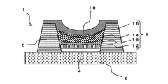
[構成]
図1は、本発明の有機EL素子の、一実施形態における概略構成例を断面で示す模式図である。図1に示すように、有機EL素子1は、基板2と、第一電極4と、隔壁6と、発光媒体層8と、第二電極10を備えている。なお、本実施形態では、一例として、有機EL素子1を、第一電極4を陽極とし、第二電極10を陰極としたアクティブマトリクス駆動型の有機EL素子とした場合について説明する。この場合、第一電極4は、画素ごとに隔壁6で区画された画素電極として形成され、第二電極10は、素子全面に形成した対向電極として形成される。なお、有機EL素子1の構成は、上記の構成に限定するものではなく、例えば、各電極(第一電極4、第二電極10)がそれぞれ直交するストライプ状とした、パッシプマトリクス駆動型の有機EL素子であってもよい。また、第一電極4を陰極とし、第二電極10を陽極とした逆構造としてもよい。
[Constitution]
FIG. 1 is a schematic diagram showing, in cross section, a schematic configuration example of one embodiment of the organic EL element of the present invention. As shown in FIG. 1, the
[基板2]
図2は、基板2の詳細な構成を示す断面図である。本実施形態では、基板2として、第一電極4及び隔壁6が設けられたTFT基板を用いた場合を例に挙げて説明する。図2に示すように、本発明の有機EL素子1が備える基板2は、薄膜トランジスタ20(TFT)と第一電極4(画素電極)が設けられている。薄膜トランジスタ20と第一電極4とは、電気接続している。また、薄膜トランジスタ20は、基板2(支持体)で支持されている。
[Substrate 2]
FIG. 2 is a cross-sectional view showing a detailed configuration of the
基板2としては、機械的強度及び絶縁性を有し、寸法安定性に優れていれば、如何なる材料も使用することが可能である。ここで、基板2の材料としては、例えば、ガラスや石英、ポリプロピレン、ポリエーテルサルフォン、ポリカーボネート、シクロオレフィンポリマー、ポリアリレート、ポリアミド、ポリメチルメタクリレート、ポリエチレンテレフタレート、ポリエチレンナフタレート等のプラスチックフィルムやシートを用いることが可能である。
As the
また、基板2の材料としては、例えば、上記のプラスチックフィルムやシートに、酸化珪素、酸化アルミニウム等の金属酸化物や、弗化アルミニウム、弗化マグネシウム等の金属弗化物、窒化珪素、窒化アルミニウム等の金属窒化物、酸窒化珪素等の金属酸窒化物、アクリル樹脂やエポキシ樹脂、シリコーン樹脂、ポリエステル樹脂等の高分子樹脂膜を単層もしくは積層させた透光性基材や、アルミニウムやステンレス等の金属箔、シート、板等を用いることが可能である。さらに、基板2の材料としては、例えば、上記のプラスチックフィルムやシートにアルミニウム、銅、ニッケル、ステンレス等の金属膜を積層させた非透光性基材等を用いることが可能である。ここで、基板2の透光性は、光の取出しをどちらの面から行うかに応じて選択すればよい。
The material of the
上記の材料からなる基板2は、有機EL素子1内への水分の侵入を避けるために、無機膜を形成したり、フッ素樹脂を塗布したりして、防湿処理や疎水性処理を施してあることが好適である。特に、発光媒体層8への水分の侵入を避けるために、基板2における含水率及びガス透過係数を小さくすることが好適である。
The
薄膜トランジスタ20としては、公知の薄膜トランジスタを用いることが可能である。具体的には、主として、ソース/ドレイン領域及びチャネル領域が形成される活性層22と、ゲート絶縁膜24及びゲート電極26から構成される薄膜トランジスタが挙げられる。ここで、薄膜トランジスタ20の構造は、特に限定されるものではなく、例えば、スタガ型、逆スタガ型、トップゲート型、コプレーナ型等が挙げられる。また、活性層22の構成は、特に限定されるものではなく、例えば、非晶質シリコン、多結晶シリコン、微結晶シリコン、セレン化カドミウム等の無機半導体材料、または、チオフェンオリゴマー、ポリ(p−フェリレンビニレン)等の有機半導体材料により形成することが可能である。
As the
上記の活性層22は、例えば、以下の(a)から(c)に記載する方法を用いて形成することが出来る。
(a)アモルファスシリコンをプラズマCVD法により積層し、イオンドーピングする方法。具体的には、SiH4ガスを用いて、LPCVD法によりアモルファスシリコンを形成し、固相成長法によりアモルファスシリコンを結晶化してポリシリコンを得た後、イオン打ち込み法によりイオンドーピングする方法。
(b)Si2H6ガスを用いたLPCVD法により、また、SiH4ガスを用いたPECVD法によりアモルファスシリコンを形成し、エキシマレーザー等のレーザーによりアニールし、さらに、アモルファスシリコンを結晶化してポリシリコンを得た後、イオンドーピング法によりイオンドーピングする方法(低温プロセス)。
(c)減圧CVD法またはLPCVD法によりポリシリコンを積層し、1000℃以上で熱酸化してゲート絶縁膜を形成し、その上にn+ポリシリコンのゲート電極8を形成し、その後、イオン打ち込み法によりイオンドーピングする方法(高温プロセス)。
The
(A) A method of laminating amorphous silicon by plasma CVD and ion doping. Specifically, using SiH 4 gas, amorphous silicon is formed by LPCVD, amorphous silicon is crystallized by solid phase growth to obtain polysilicon, and then ion doping is performed by ion implantation.
(B) Amorphous silicon is formed by LPCVD using Si 2 H 6 gas or PECVD using SiH 4 gas, annealed by a laser such as an excimer laser, and then amorphous silicon is crystallized to form poly After silicon is obtained, ion doping is performed by an ion doping method (low temperature process).
(C) Polysilicon is laminated by low pressure CVD or LPCVD, thermally oxidized at 1000 ° C. or higher to form a gate insulating film, an n +
ゲート絶縁膜24としては、一般的にゲート絶縁膜として使用されているものを用いることが可能である。すなわち、ゲート絶縁膜24としては、例えば、PECVD法、LPCVD法等により形成されたSiO2や、ポリシリコン膜を熱酸化して得られるSiO2等を用いることが可能である。ゲート電極26としては、一般的にゲート電極として使用されているものを用いることが可能である。すなわち、ゲート電極26の材料としては、例えば、アルミ、銅等の金属(チタン、タンタル、タングステン等の高融点金属)や、ポリシリコン、高融点金属のシリサイド、ポリサイド等が挙げられる。
As the
なお、薄膜トランジスタ20の構造は、シングルゲート構造、ダブルゲート構造、ゲート電極が三つ以上のマルチゲート構造であってもよい。また、LDD構造、オフセット構造を有していてもよい。さらに、一つの画素中に二つ以上の薄膜トランジスタが配置されていてもよい。また、本実施形態の有機EL素子1は、薄膜トランジスタ20が有機EL素子1のスイッチング素子として機能するように接続されている必要がある。このため、薄膜トランジスタ20のドレイン電極28と、第一電極4を電気的に接続している。なお、図2では、ソース電極に符号30を付し、走査線に符号32を付し、薄膜トランジスタ20と第一電極4及び隔壁6との間に介装したトランジスタ絶縁膜に、符号34を付している。
Note that the structure of the
[第一電極4]
次に、第一電極4の詳細な構成について説明する。第一電極4は、基板2上にパターン化して形成されており、隔壁6によって区画されて、各画素に対応した画素電極を形成している。第一電極4の材料としては、ITO(インジウムスズ複合酸化物)やインジウム亜鉛複合酸化物、亜鉛アルミニウム複合酸化物等の金属複合酸化物や、金、白金等の金属材料や、これら金属酸化物や金属材料の微粒子をエポキシ樹脂やアクリル樹脂等に分散した微粒子分散膜を、単層もしくは積層したものを、いずれも使用することが可能である。
[First electrode 4]
Next, a detailed configuration of the
ここで、第一電極4を陽極とする場合には、ITO等の仕事関数の高い材料を選択することが好適である。特に、通常の有機EL素子では、陽極を通して光が放出されるために、陽極が透明であることが要求され、ITO等の導電性金属酸化物が用いられる。また、有機EL素子が、上方から光を取り出す、いわゆるトップエミッション構造の場合は、透明であることは必要ではないが、ITO、IZO(インジウムと亜鉛の複合酸化物)等の導電性金属酸化物を用いて、第一電極を形成してもよい。
Here, when the
さらに、第一電極4の材料として、ITO等の導電性金属酸化物を用いる場合、その下に反射率の高い反射電極(Cr、A1、Ag、Mo、W等)を用いることが好適である。この場合、反射電極は、導電性金属酸化物よりも抵抗率が低いため、補助電極として機能するとともに、後述する有機発光層14にて発光される光を、第二電極10側に反射して、光の有効利用を図ることが可能となる。また、有機EL素子が、下方から光を取り出す、いわゆるボトムエミッション構造の場合は、透光性のある材料を選択する必要がある。さらに、必要に応じて、第一電極4の配線抵抗を低くするために、銅やアルミニウム等の金属材料を補助電極として併設してもよい。
Further, when a conductive metal oxide such as ITO is used as the material of the
[隔壁6]
次に、隔壁6の詳細な構成について説明する。隔壁6は、基板2上に形成されており、第一電極4の周囲を囲むことにより、画素に対応した発光領域を区画するように形成されている。ここで、一般的に、アクティブマトリクス駆動型の有機EL素子は、各画素(サブピクセル)に対して第一電極が形成されており、それぞれの画素が、できるだけ広い面積を占有しようとするため、第一電極の端部(側面)を覆うように形成される隔壁の最も好適な形状は、第一電極を最短距離で区切る格子状を基本とする。
[Partition 6]
Next, the detailed structure of the
また、隔壁6の材料は、少なくとも、エチレン性不飽和化合物、光重合開始剤及びアルカリ可溶性バインダーを含有する。さらに、隔壁6の材料は、界面活性剤等を含有することが好適であり、溶剤も含有している。隔壁6の好適な高さは、0.1μm以上10μm以下の範囲内であり、より好適には、0.5μm以上2μm以下の範囲内である。その理由は、隔壁6の高さが高すぎる場合は、第二電極10(対向電極)の形成及び封止が妨げられ、隔壁6の高さが低すぎる場合は、第一電極4の端部を覆い切れず、また、発光媒体層8の形成時に隣接する画素と混色してしまうためである。
Moreover, the material of the
隔壁6の断面形状としては、順テーパ形状、逆テーパ形状等の台形状や、半円形等が挙げられ、また、多段状になっていても良い。ここで、隔壁6の断面形状が多段状である場合には、下の基板側の下段と上の基板側の上段とが異なる材料・形成方法であっても、同じ材料・形成方法であってもよい。この場合、例えば、下段はSiN等の無機材料からなり、上段は上述した材料からなる構成等が挙げられる。
Examples of the cross-sectional shape of the
[発光媒体層8]
次に、発光媒体層8の詳細な構成について説明する。発光媒体層8は、隔壁6内で第一電極4上に形成されて、第一電極4と第二電極10との間に挟持されており、正孔注入層12と、有機発光層14と、第一電子注入層16と、第二電子注入層17と、インターレイヤー層18を含んでいる。正孔注入層12は、電子または正孔を注入するキャリア注入層を構成しており、第一電極4上及び隔壁6上、具体的には、第一電極4上と、隔壁6上の全面とを覆うように形成されている。これにより、画素領域での膜形状が平坦になるため、画素ごとの膜厚を均一にすることが可能となる。
[Luminescent medium layer 8]
Next, a detailed configuration of the light emitting
なお、正孔注入層12の詳細な構成については、後述する。有機発光層14は、発光に寄与する層であり、正孔注入層12上に形成されている。すなわち、正孔注入層12は、有機発光層14の下に形成されている。また、有機発光層14は、隔壁6から離れた部分
ほど厚さが減少しており、その中心において、厚さが最小となっている。なお、有機発光層14の詳細な構成については、後述する。第一電子注入層16と、第二電子注入層17は、電子を注入する層であり、有機発光層14上に形成されている。また、第一電子注入層16は隔壁6の上部を覆わないよう形成され、第二電子注入層17は隔壁6の一部を覆うように形成されている。なお、電子注入層の詳細な構成については、後述する。
The detailed configuration of the
インターレイヤー層18は、正孔注入層12と有機発光層14との間に形成されて、正孔注入層12及び有機発光層14と積層している。また、インターレイヤー層18は、電子注入層や電子ブロック層を形成している。また、発光媒体層8は、隔壁6内で第一電極4上に形成されることにより、有機EL素子1を、画素(サブピクセル)として配列することを可能とし、画像表示装置とすることが可能となる。すなわち、各画素を構成する有機発光層14を混色することなく、例えば、R(赤色)、G(緑色)及びB(青色)の三色に塗り分けることで、フルカラーのディスプレイパネルを作製することが可能となる。
The
[正孔注入層12]
次に、正孔注入層12の詳細な構成について説明する。正孔注入層12の膜厚は、20nm以上100nm以下の範囲内であることが好適である。これは、正孔注入層12の膜厚が20nmよりも薄くなると、ショート欠陥が生じやすくなり、また、正孔注入層12の膜厚が100nmを超えると、高抵抗化により低電流化してしまうためである。
[Hole Injection Layer 12]
Next, a detailed configuration of the
正孔注入層12の材料としては、例えば、ポリアニリン誘導体、ポリチオフェン誘導体、ポリビニルカルバゾール(PVK)誘導体、ポリ(3,4−エチレンジオキシチオフェン)(PEDOT)等が挙げられる。これらの材料は、溶媒に溶解または分散させ、スピンコーター等を用いた各種塗布方法や凸版印刷方法を用いることにより、正孔注入層12を形成する。
Examples of the material for the
また、正孔注入層12の材料として無機材料を用いる場合、無機材料としては、例えば、Cu2O、Cr2O3、Mn2O3、FeOx(x〜0.1)、NiO、CoO、Pr2O3、Ag2O、MoO2、Bi2O3、ZnO、TiO2、SnO2、ThO2、V2O5、Nb2O5、Ta2O5、MoO3、WO3、MnO2等の無機材料を用いる。そして、蒸着法、または、スパッタリング法を用いて、正孔注入層12を形成する。ただし、上記の材料は、これらに限定されるものではない。
When an inorganic material is used as the material for the
[有機発光層14]
次に、有機発光層14の詳細な構成について説明する。有機発光層14は、正孔と電子を再結合させることで発光する層であり、有機発光層14から放出される表示光が単色の場合は、インターレイヤー層18を被覆するように形成するが、多色の表示光を得るためには、必要に応じてパターニングを行うことにより、好適に用いることが可能である。
[Organic light-emitting layer 14]
Next, the detailed structure of the organic
有機発光層14を形成する有機発光材料は、例えば、クマリン系、ペリレン系、ピラン系、アンスロン系、ポルフィレン系、キナクリドン系、N,N’−ジアルキル置換キナクリドン系、ナフタルイミド系、N,N’−ジアリール置換ピロロピロール系、イリジウム錯体系等の発光性色素を、ポリスチレン、ポリメチルメタクリレート、ポリビニルカルバゾール等の高分子中に分散させたものや、ポリアリーレン系、ポリアリーレンビニレン系やポリフルオレン系の高分子材料が挙げられるが、本実施形態では、これらの材料に限定するものではない。
Examples of the organic light-emitting material forming the organic light-emitting
また、上記の有機発光材料は、溶媒に溶解または安定に分散させることにより、有機発光インキとなる。ここで、有機発光材料を溶解または分散する溶媒としては、トルエン、キシレン、アセトン、アニソール、メチルエチルケトン、メチルイソブチルケトン、シク
ロヘキサノン等の単独、または、これらの混合溶媒が挙げられる。特に、トルエン、キシレン、アニソールといった芳香族有機溶媒が、有機発光材料の溶解性の面から好適である。また、上記の有機発光インキには、必要に応じて、界面活性剤、酸化防止剤、粘度調整剤、紫外線吸収剤等が添如されていてもよい。
Moreover, said organic luminescent material becomes organic luminescent ink by melt | dissolving in a solvent or disperse | distributing stably. Here, examples of the solvent for dissolving or dispersing the organic light emitting material include toluene, xylene, acetone, anisole, methyl ethyl ketone, methyl isobutyl ketone, cyclohexanone, and the like, or a mixed solvent thereof. In particular, aromatic organic solvents such as toluene, xylene, and anisole are preferable from the viewpoint of the solubility of the organic light emitting material. Moreover, surfactant, antioxidant, a viscosity modifier, a ultraviolet absorber, etc. may be added to said organic light emitting ink as needed.
[第一電子注入層16、第二電子注入層17]
以下、第一電子注入層16と第二電子注入層17の詳細な構成について説明する。本発明においては、有機発光層14の厚みにより最適なキャリアバランスが異なるため、膜厚分布が存在する有機発光層14上に設けた電子注入層は第一電子注入層16と第二電子注入層17に分けて形成させている。第一電子注入層16及び第二電子注入層17の材料としては、透過性が高く、有機発光層14への電子注入効率が高い、さらに仕事関数の小さい材料を用いる。この場合、具体的な材料としては、Ca、Cs、LiF、BaF2等の、アルカリ金属及びアルカリ土類金属の化合物が挙げられる。これ以外にも、電子注入層16の材料としては、例えば、有機材料として、A1q3等が挙げられる。前述で挙げた材料の中から、キャリアバランスを考慮し第一電子注入層16と第二電子注入層17の材料選択を行う。例えば、前述で設けた有機発光層14が電子輸送性の高い材料であれば、有機発光層14の膜厚が厚くなると導電性が悪くなり電子の注入性が低下するため、厚膜部上には仕事関数が小さいなど電子注入性が高くなる材料を選択することが好ましい。また、有機発光層14が正孔輸送性の高い材料であれば、逆にキャリアバランスを考え厚膜部上に仕事関数が高いなど電子注入性の低くなる材料を選択する。ただし、上述した材料の選定に限定するものではない。
[First electron injection layer 16, second electron injection layer 17]
Hereinafter, detailed configurations of the first electron injection layer 16 and the second
第一電子注入層16と第二電子注入層17の形成領域としては、有機発光層14の中心から隔壁6へ向かう方向で、有機発光層14の膜厚が中心部の膜厚に対して0〜30nm未満まで増加する領域には第一電子注入層16を設け、有機発光層14の膜厚が中心部の膜厚に対して30nm以上増加する領域には第二電子注入層17が設けられているように形成されている。また、第一電子注入層16は有機発光層14の中心から隔壁6へ向かう方向へ、画素内の中心発光強度から50%低下する領域まで設けるように形成されている。
As a region where the first electron injection layer 16 and the second
[第二電極10]
第二電極10は、基板2及び発光媒体層8上に形成されており、第一電極4と対向している。ここで、第二電極10は、例えば、第一電子注入層16及び第二電子注入層への、水や酸素の浸入を防ぐために、隔壁6及び発光媒体層8全体を覆うように形成する。第二電極10の材料としては、第二電極10を陰極とする場合には、例えば、Mg、A1、Yb等の金属単体を用いる。
[Second electrode 10]
The
[封止体]
有機EL素子1を、前述したトップエミッション方式で作成する場合、発光媒体層8から、基板2と反対側の封止体を通して放射される表示光を取り出すためには、可視光波長領域に対して、光透過性が必要となる。また、有機EL素子1は、電極(第一電極4、第二電極10)間に発光材料(発光媒体層8)を挟み、電流を流すことで発光させることが可能であるが、有機発光層14の材料である有機発光材料は、大気中の水分や酸素によって容易に劣化してしまう。このため、通常、有機EL素子1には、外部と遮断するための封止体(図示せず)を設ける。このような封止体は、例えば、封止材上に樹脂層を設けて形成することが可能である。
[Sealed body]
When the
上記の封止材の材料としては、水分や酸素の透過性が低い基材を用いる必要がある。ここで、封止材の材料としては、例えば、アルミナ、窒化ケイ素、窒化ホウ素等のセラミックス、無アルカリガラス、アルカリガラス等のガラス、石英、耐湿性フィルム等を挙げることができる。耐湿性フィルムとしては、例えば、プラスチック基材の両面にSiOxを
CVD法で形成したフィルムや、透過性の小さいフィルムと吸水性のあるフィルム、または、吸水剤を塗布した重合体フィルム等がある。ここで、耐湿性フィルムの水蒸気透過率は、10−6g/m2/day以下であることが好適である。
As a material for the sealing material, it is necessary to use a base material having low moisture and oxygen permeability. Here, examples of the material for the sealing material include ceramics such as alumina, silicon nitride, and boron nitride, glass such as alkali-free glass and alkali glass, quartz, and a moisture-resistant film. Examples of the moisture-resistant film include a film in which SiOx is formed on both surfaces of a plastic substrate by a CVD method, a film having a low permeability and a water absorption property, or a polymer film coated with a water absorbing agent. Here, the water vapor transmission rate of the moisture-resistant film is preferably 10 −6 g / m 2 / day or less.
封止材上に設ける樹脂層の材料としては、例えば、エポキシ系樹脂、アクリル系樹脂、シリコン樹脂等からなる光硬化型接着性樹脂、熱硬化型接着性樹脂、二液硬化型接着性樹脂や、エチレンエチルアクリレート(EEA)ポリマー等のアクリル系樹脂、エチレンビニルアセテート(EVA)等のビニル系樹脂、ポリアミド、合成ゴム等の熱可塑性樹脂や、ポリエチレンやポリプロピレンの酸変性物等の熱可塑性接着性樹脂を挙げることができる。 Examples of the resin layer material provided on the sealing material include a photo-curable adhesive resin, a thermosetting adhesive resin, a two-component curable adhesive resin made of an epoxy resin, an acrylic resin, a silicon resin, and the like. , Acrylic resins such as ethylene ethyl acrylate (EEA) polymer, vinyl resins such as ethylene vinyl acetate (EVA), thermoplastic resins such as polyamide and synthetic rubber, and thermoplastic adhesives such as acid-modified products of polyethylene and polypropylene Resins can be mentioned.
また、樹脂層を封止材の上に形成する方法としては、例えば、溶剤溶液法、押出ラミネーション法、溶融・ホットメルト法、カレンダー法、ノズル塗布法、スクリーン印刷法、真空ラミネート法、熱ロールラミネート法等を挙げることができる。この場合、必要に応じて、吸湿性や吸酸素性を有する材料を含有させることも可能である。ここで、封止材上に形成する樹脂層の厚みは、封止する有機EL表示装置の大きさや形状により任意に決定されるが、5μm以上500μm以下の範囲内が好適である。 Examples of the method for forming the resin layer on the sealing material include a solvent solution method, an extrusion lamination method, a melt / hot melt method, a calendar method, a nozzle coating method, a screen printing method, a vacuum laminating method, and a hot roll. The laminating method etc. can be mentioned. In this case, it is possible to contain a hygroscopic or oxygen-absorbing material as necessary. Here, the thickness of the resin layer formed on the sealing material is arbitrarily determined depending on the size and shape of the organic EL display device to be sealed, but is preferably in the range of 5 μm to 500 μm.
上記の説明では、封止体を、封止材上に樹脂層として形成したが、封止体を、有機EL素子1側に、直接形成することも可能である。また、有機EL素子1と封止体との貼り合わせは、封止室で行う。ここで、封止体を、封止材と樹脂層の二層構造とし、樹脂層に熱可塑性樹脂を使用した場合は、加熱したロールで圧着のみ行うことが好適である。一方、樹脂層に熱硬化型接着樹脂を使用した場合は、加熱したロールで圧着した後、さらに、硬化温度で加熱硬化を行うことが好適である。また、樹脂層に光硬化性接着樹脂を使用した場合は、ロールで圧着した後、さらに光を照射することで硬化を行うことが可能である。
In the above description, the sealing body is formed as a resin layer on the sealing material. However, the sealing body can be directly formed on the
また、上述したような封止材を用いて封止を行う前や、その代わりに、例えば、パッシベーション膜として、EB蒸着法やCVD法等のドライプロセスを用いて、窒化珪素膜等無機薄膜による封止体を用いることも可能である。また、これらを組み合わせた封止体を用いることも可能である。この場合、上述したパッシベーション膜の膜厚は、100nm以上500nm以下の範囲内とすることが可能である。特に、材料の透湿性や、光透過性等により異なるが、パッシベーション膜の膜厚を、150nm以上300nm以下の範囲内とすることが好適である。また、有機EL素子1を、前述したトップエミッション型の構造とした場合、上記の特性に加え、光透過性を考慮する必要があるため、可視光波長領域の全平均で70%以上であれば好適である。
Moreover, before sealing using the sealing material as described above, or instead, for example, as a passivation film, a dry process such as an EB vapor deposition method or a CVD method is used, and an inorganic thin film such as a silicon nitride film is used. It is also possible to use a sealing body. Moreover, it is also possible to use the sealing body which combined these. In this case, the thickness of the passivation film described above can be in the range of 100 nm to 500 nm. In particular, the thickness of the passivation film is preferably in the range of 150 nm to 300 nm, although it varies depending on the moisture permeability and light transmittance of the material. In addition, when the
[有機EL素子1の製造方法]
以下、図1及び2を参照しつつ、図3を用いて、本発明の有機EL素子1の製造方法を説明する。有機EL素子1を製造する際には、まず、基板2上に第一電極4を形成する第一電極形成工程を行う。すなわち、有機EL素子1の製造方法には、第一電極形成工程を含む。第一電極形成工程において、第一電極4を形成する方法としては、第一電極4の材料に応じて、抵抗加熱蒸着法、電子ビーム蒸着法、反応性蒸着法、イオンプレーティング法、スパッタリング法等の乾式成膜法を用いることが可能である。また、第一電極4を形成する方法としては、乾式成膜法以外にも、グラビア印刷法や、スクリーン印刷法等の湿式成膜法等を用いることが可能である。
[Method for Manufacturing Organic EL Element 1]
Hereinafter, the manufacturing method of the
ここで、第一電極4のパターニング方法としては、第一電極4の材料や成膜方法に応じて、マスク蒸着法、フォトリソグラフィ法、ウェットエッチング法、ドライエッチング法等の既存のパターニング法を用いることが可能である。なお、基板2としてTFTを形成した基板(図2参照)を用いる場合は、下層の画素に対応して導通を図ることができるよ
うに形成する。
Here, as a patterning method for the
そして、基板2上に第一電極4を形成した後、第一電極4の周囲を囲む隔壁6を基板2上に形成する隔壁形成工程を行う。すなわち、有機EL素子1の製造方法には、隔壁形成工程を含む。隔壁形成工程において、第一電極4を形成した基板2上に隔壁6を形成する方法としては、例えば、第一電極4を形成した基板2上に無機膜を一様に形成し、レジストでマスキングした後、ドライエッチングを行う方法や、第一電極4を形成した基板2上に感光性樹脂を積層し、フォトリソ法により所定のパターンとする方法が挙げられる。
And after forming the
また、必要に応じて、隔壁6の材料に、撥水剤を添加することや、プラズマやUVを照射して、隔壁6の形成後に、隔壁6に対して、インクに対する撥液性を付与することも可能である。隔壁形成工程により基板2上に隔壁6を形成した後、発光媒体層8を第一電極4上に形成する発光媒体層形成工程を行う。すなわち、有機EL素子1の製造方法には、発光媒体層形成工程を含む。
Further, if necessary, a water repellent is added to the material of the
発光媒体層形成工程は、正孔注入層12を第一電極4上を覆うように形成する正孔注入層形成工程と、有機発光層14を正孔注入層12上に形成する有機発光層形成工程と、第1電子注入層16と第2電子注入層17を有機発光層14上に形成する電子注入層形成工程を含む。正孔注入層形成工程では、正孔注入層12の材料に応じて、正孔注入層12の材料を溶媒に溶解または分散させ、スピンコーター等を用いた各種塗布方法やスリットコート法、スプレーコート法、バーコート法、ディップコート法、凸版印刷法によって形成する方法や、抵抗加熱蒸着法によって形成する方法を用いる。
In the light emitting medium layer forming step, a hole injecting layer forming step for forming the
また、これらの方法以外に、例えば、抵抗加熱蒸着法、電子ビーム蒸着法、反応性蒸着法、イオンプレーティング法、スパッタリング法等のドライ成購法や、スピンコート法、ゾルゲル法等のウェット成膜法等、既存の成膜法を用いてもよい。ここで、発光媒体層8が含む層(正孔注入層12、有機発光層14、第1電子注入層16、第2電子注入層17)のうち少なくとも一つの層は、ウェットプロセス法を用いて形成する。
In addition to these methods, for example, dry heating methods such as resistance heating vapor deposition, electron beam vapor deposition, reactive vapor deposition, ion plating, and sputtering, and wet chemical such as spin coating and sol-gel methods. An existing film formation method such as a film method may be used. Here, at least one of the layers included in the light emitting medium layer 8 (the
有機発光層形成工程では、有機発光層14の材料に応じて、インクジェット印刷法、ノズルプリント印刷法、凸版印刷法、グラビア印刷法、スクリーン印刷法等のウェット成膜法等既存の成膜法を用いる。特に、有機発光材料を、溶媒に溶解、または、安定に分散させた有機発光インキを用いて、有機発光層14を各発光色に塗り分ける場合には、隔壁6間にインキを転写してパターニングできるインクジェット法、ノズルプリント法、凸版印刷法が好適である。
In the organic light emitting layer forming step, an existing film forming method such as an ink jet printing method, a nozzle print printing method, a relief printing method, a gravure printing method, a screen printing method or the like is used according to the material of the organic
すなわち、有機発光層形成工程では、第一電極4上を覆うように形成された正孔注入層12上に、有機発光層14の材料である有機発光材料を溶媒に溶解または分散させた有機発光インキを塗工して、有機発光層14をパターン化して形成する。また、有機発光層形成工程は、印刷法、インクジェット法及びノズルプリント法のうちいずれかを用いて行う。なお、上述した成膜法以外の方法を用いて、有機発光層14を形成してもよい。
That is, in the organic light emitting layer forming step, organic light emission in which an organic light emitting material as a material of the organic
ここで、図3を用いて、凸版印刷法により、有機発光層14を形成する手順を説明する。図3は、凸版印刷法に用いる凸版印刷装置36の概略構成を示す図である。図3に示すように、凸版印刷装置36は、有機発光材料からなる有機発光インキを、第一電極4、正孔注入層12、インターレイヤー層18が形成された基板2上にパターン印刷する際に用いる装置であり、インクタンク38と、インキチャンバー40と、アニロックスロール42と、凸部が設けられた凸版44がマウントされた版胴46を有している。
Here, the procedure for forming the organic
インクタンク38には、溶剤で希釈された有機発光インキが収容されており、インキチ
ャンバー40には、インクタンク38から、有機発光インキが送り込まれるようになっている。アニロックスロール42は、インキチャンバー40のインキ供給部に接して、インキチャンバー40へ回転可能に支持されている。
The
上記のパターン印刷を行う際には、アニロックスロール42の回転に伴い、アニロックスロール42の表面に供給された有機発光インキのインキ層48が、均一な膜厚に形成される。このインキ層48のインキは、アニロックスロール42に近接して回転駆動される版胴46にマウントされた凸版44の凸部に転移する。そして、ステージ50に、被印刷基板(基板2)が設置されており、凸版44の凸部にあるインキが基板2に対して印刷され、必要に応じて乾燥工程を経て、基板2上に有機発光層14が形成されることとなる。
When the pattern printing is performed, the
なお、他の発光媒体層(例えば、インターレイヤー層18)をインキ化して塗工する場合についても、上記と同様の形成方法を用いて、基板2上に層を形成することが可能である。ここで、本実施形態の有機EL素子1は、発光媒体層8が、正孔注入層12と、有機発光層14と、電子注入層16に加え、インターレイヤー層18を含んでいる。このため、本実施形態では、有機発光層形成工程の後工程として、インターレイヤー層18を形成するインターレイヤー層形成工程を行う。すなわち、本実施形態では、発光媒体層形成工程が、インターレイヤー層18を形成するインターレイヤー層形成工程を含んでいる。
In addition, also about the case where other luminescent medium layers (for example, interlayer layer 18) are made into ink and applied, it is possible to form a layer on the
インターレイヤー層形成工程において、インターレイヤー層18を形成する際には、インターレイヤー層18の材料として、ポリビニルカルバゾール、またはその誘導体、側鎖または主鎖に芳香族アミンを有するポリアリーレン誘導体、アリールアミン誘導体、トリフェニルジアミン誘導体等の、芳香族アミンを含むポリマー等を用い、これらの材料を、溶媒に溶解または分散させ、スピンコーター等を用いた各種塗布方法やインクジェット法、ノズルプリント法、凸版印刷法、スリットコート法、バーコート法を用いて形成する。
In forming the
次に、画素内の有機発光層上に形成する各電子注入層の成膜工程として、図4(a)、(b)、(c)に示す異なるマスクパターンを用いて成膜する。第一電子注入層16は図4(a)のような中心部が空洞かつ隔壁上部を覆わないマスクで、第二電子注入層17は図4(b)、(c)のような中心部が遮蔽かつ隔壁上部の一部を覆うマスクでパターン形成する。ただし、上述したこれらマスクパターンに限定するものではない。成膜手法としては材料に応じ、抵抗過熱法、電子ビーム蒸着法、反応性蒸着法、イオンプレーティング法、スパッタ法等を用いて、第一電子注入層16及び第二電子注入層17を形成する。
Next, as a film forming process of each electron injection layer formed on the organic light emitting layer in the pixel, films are formed using different mask patterns shown in FIGS. 4 (a), 4 (b), and 4 (c). The first electron injection layer 16 is a mask having a hollow central portion as shown in FIG. 4A and does not cover the upper part of the partition wall, and the second
上述した発光媒体層形成工程により発光媒体層8を形成した後、基板2及び発光媒体層8上に、第二電極10を形成する第二電極形成工程を行う。すなわち、有機EL素子1の製造方法には、第二電極形成工程を含む。第二電極形成工程において、第二電極10を形成する方法としては、第二電極10の材料に応じて、抵抗加熱蒸着法、電子ビーム蒸着法、反応性蒸着法、イオンプレーティング法、スパッタリング法等の乾式成膜法を用いることが可能である。第二電極10を形成した後、上述した封止体を形成して、有機EL素子1の製造を終了する。
After the light emitting
以上説明した如く、本実施形態の有機EL素子1の構成、及びその製造方法であれば、最適なキャリアバランスを考慮して有機発光層14上に形成する第一電子注入層16と第二電子注入層17の形成領域を分けることで、有機発光層14の膜厚の厚い部分が発光し、かつ輝度が向上する。その結果、画素内での発光領域が拡がりかつ画素内全輝度の増加が可能な、有機EL素子1及びその製造方法を提供することが可能となる。
As described above, the first electron injection layer 16 and the second electron formed on the organic
本発明の有機EL素子は、上述した実施形態例以外にも可能であり、例えば、以下に列挙する構成及び製造方法が可能である。
(1)本実施形態の有機EL素子1では、発光媒体層8の構成を、正孔注入層12と、有機発光層14と、インターレイヤー層18を含んでいる構成としたが、これに限定するものではなく、発光媒体層8の構成を、インターレイヤー層18を含んでいない構成としてもよい。
(2)本実施形態の有機EL素子1の製造方法では、発光媒体層形成工程が、インターレイヤー層18を形成するインターレイヤー層形成工程を含んでいるが、これに限定するものではなく、発光媒体層形成工程が、インターレイヤー層形成工程を含んでいなくともよい。
The organic EL element of the present invention is possible in addition to the above-described embodiment examples. For example, the configurations and manufacturing methods listed below are possible.
(1) In the
(2) In the manufacturing method of the
以下に、本発明の具体的実施例について説明する。 Specific examples of the present invention will be described below.
図1から図4を参照しつつ、図5を用いて、上述した第一実施形態の有機EL素子1と、比較例の有機EL素子を製造し、両者に対する物性の評価を行った結果について説明する。なお、以下の説明では、第一実施形態の有機EL素子1を、「本発明例の有機EL素子」と記載する。同様に、以下の説明では、比較例の有機EL素子を、「比較例の有機EL素子」と記載する。
With reference to FIG. 1 to FIG. 4, the results of manufacturing the
<実施例1>
本発明例の有機EL素子を製造する際に、基板2として、基板2上に設けられたスイッチング素子として機能する薄膜トランジスタ20と、その上方に形成された第一電極4(画素電極)とを備えたアクティブマトリクス基板を用いた。また、アクティブマトリクス基板(基板2)のサイズは、200mm×200mmである。さらに、上記のアクティブマトリクス基板は、その中に5型の、画素数が320×240のディスプレイが中央に配置されている。
<Example 1>
When manufacturing the organic EL element of the present invention example, the
まず、上記のアクティブマトリクス基板上に、スパッタ法を用いて、厚さ150nmのITO膜を形成し、これを第一電極4とした。さらに、第一電極4の周囲を囲んで画素を区画するような形状で、隔壁6を形成した。ここで、隔壁6を形成する際には、まず、アクリル系のフォトレジスト材料を、アクティブマトリクス基板の全面に厚さ2μmで形成した後、上記のフォトレジスト材料に対して、フォトリソグラフィ法により、第一電極4上に幅30μmの隔壁6を形成した。各画素の幅は80μm×150μmとなった。
First, an ITO film having a thickness of 150 nm was formed on the above active matrix substrate by sputtering, and this was used as the
次に、上記のように形成した第一電極4及び隔壁6上に、厚さ20nmの酸化モリブデン(MoOx)を、スパッタリング製膜により成膜して、正孔注入層12を形成した。そして、インターレイヤー層18の材料であるポリビニルカルバゾール誘導体を、濃度が0.5%となるようにトルエンに溶解させたインキを用いて、上記のアクティブマトリクス基板を印刷機にセッティングし、絶縁層に挟まれた第一電極4の真上に、そのラインパターンに合わせて、凸版印刷法で印刷し、その後乾燥を行った。このとき、300線/2.54cmのアニロックスロール及び感光性樹脂版を使用した。インターレイヤー層18の狙い膜厚は、20nmとして印刷した。
Next, molybdenum oxide (MoOx) having a thickness of 20 nm was formed on the
次に、有機発光材料であり、かつ電子輸送性の高いポリフェニレンビニレン誘導体を用いて、その濃度が1%となるようにトルエンに溶解させて有機発光インキとし、上記のアクティブマトリクス基板を印刷機にセッティングし、絶縁層に挟まれた第一電極4の真上に、そのラインパターンに合わせて、有機発光層14を凸版印刷法で印刷し、その後乾燥を行った。このとき、150線/2.54cmのアニロックスロール42及び水現像タイプの感光性樹脂板を使用した。有機発光層14の狙い膜厚は60nmとして印刷した。
Next, a polyphenylene vinylene derivative that is an organic light emitting material and has a high electron transporting property is dissolved in toluene so that its concentration becomes 1% to obtain an organic light emitting ink, and the above active matrix substrate is used in a printing machine. After setting, the organic
次に、第一電子注入層16と第二電子注入層17を、第一電子注入層16には図4(a
)に示したメタルマスクを用いて、第二電子注入層17には図4(b)及び(c)に示したメタルマスクを用いて、真空蒸着法により成膜する。材料の選択としては、有機発光層14に電子輸送性の高い材料を用いているため、第一電子注入層16にはCa(LUMO:2.9eV)を、第二電子注入層17にはCs(LUMO:1.9eV)を用いて、膜厚はそれぞれ4nm形成した。これにより、第一電子注入層16を、有機発光層14の厚さが最も薄い中心から隔壁へ向かう方向へ、厚さが30nm未満厚い領域まで、さらに、画素内の中心発光強度の55%低下する領域まで形成した。第二電子注入層17は、有機発光層14の厚さが最も薄い中心から隔壁へ向かう方向へ、厚さが30nm以上増加する領域に形成した。
Next, the first electron injection layer 16 and the second
The second
さらに、第二電極10として、アルミニウム膜を、メタルマスクを用いた真空蒸着法により、隔壁6及び発光媒体層8の上面を覆う広さで、厚みが150nmとなるように成膜した。そして、上記した第二電極10を成膜したアクティブマトリクス基板に対し、封止材としたガラス板を、発光領域全てをカバーするように載せた後、約90℃で一時間程度、接着剤を熱硬化させて封止を行った。
Further, as the
<比較例1>
比較例の有機EL素子は、第一電子注入層16を、有機発光層14全体を覆うように形成し、第二電子注入層17は形成せずに作製した。その他の材料、各層の厚さ、工程は、上述した実施例1と同様とした。
<Comparative Example 1>
In the organic EL device of the comparative example, the first electron injection layer 16 was formed so as to cover the entire organic
[実施例1及び比較例1の物性評価]
上記の手順によって得られた、実施例1と、比較例1の有機EL素子に対して、画素内の輝度分布を測定した。図5は、実施例1及び比較例1の有機EL素子の画素中心を通る短辺方向の画素幅に対しての輝度依存性を表したグラフである。図5に示すように、本発明の有機EL素子である実施例1の画素内発光領域は比較例1よりも拡がり、輝度比較では、比較例が90cd/m2に対して本発明例が140cd/m2と特性向上した結果を得た。
[Evaluation of physical properties of Example 1 and Comparative Example 1]
The luminance distribution in the pixels was measured for the organic EL elements of Example 1 and Comparative Example 1 obtained by the above procedure. FIG. 5 is a graph showing the luminance dependence with respect to the pixel width in the short side direction passing through the pixel center of the organic EL elements of Example 1 and Comparative Example 1. As shown in FIG. 5, the in-pixel light emitting area of Example 1 which is the organic EL element of the present invention is larger than that of Comparative Example 1. In luminance comparison, the comparative example is 90 cd / m 2 and the present invention example is 140 cd. / M 2 and improved characteristics were obtained.
1・・・有機EL素子 2・・・基板 4・・・第1電極 6・・・隔壁
8・・・発光媒体層 10・・・第二電極 12・・・正孔注入層
14・・・有機発光層 16・・・第一電子注入層 17・・・第二電子注入層 18・・・インターレイヤー層 20・・・薄膜トランジスタ 22・・・活性層
24・・・ゲート絶縁膜 26・・・ゲート電極 28・・・ドレイン電極
30・・・ソース電極 32・・・走査線 34・・・トランジスタ絶縁膜
36・・・凸版印刷装置 38・・・インクタンク 40・・・インキチャンバー
42・・・アニロックスロール 44・・・凸版 46・・・版胴
48・・・インキ層 50・・・ステージ
DESCRIPTION OF
8 ... luminescent
DESCRIPTION OF
24 ...
30 ... Source electrode 32 ... Scanning
36 ...
42 ... Anilox roll 44 ... Letterpress 46 ... Plate cylinder
48 ...
Claims (7)
前記発光媒体層は、前記隔壁から離れた部分ほど膜厚が減少している有機発光層を含み、前記有機発光層上に第一電子注入層と第二電子注入層が形成され、且つ、前記第一電子注入層は前記隔壁の上部を覆わないよう形成され、前記第二電子注入層は一部が前記隔壁を覆うように形成されていることを特徴とする有機エレクトロルミネッセンス素子。 A substrate, a first electrode formed on the substrate, a partition wall formed on the substrate and surrounding the first electrode, and a light emitting medium layer formed on the first electrode in the partition wall; In the organic electroluminescence device comprising the second electrode formed on the partition and the light emitting medium layer,
The light-emitting medium layer includes an organic light-emitting layer having a thickness that decreases toward a portion away from the partition wall, a first electron injection layer and a second electron injection layer are formed on the organic light-emitting layer, and An organic electroluminescence device, wherein the first electron injection layer is formed so as not to cover an upper portion of the partition wall, and the second electron injection layer is formed so as to partially cover the partition wall.
前記発光媒体層を構成する層のうち少なくとも1つの層は、ウェットプロセス法を用いて形成されていることを特徴とする有機エレクトロルミネッセンス素子の製造方法。 It is a manufacturing method of the organic electroluminescent element which manufactures the organic electroluminescent element of any one of Claims 1-6,
At least one of the layers constituting the light emitting medium layer is formed using a wet process method.
Priority Applications (1)
| Application Number | Priority Date | Filing Date | Title |
|---|---|---|---|
| JP2011074807A JP2012209464A (en) | 2011-03-30 | 2011-03-30 | Organic electroluminescent element and manufacturing method for the same |
Applications Claiming Priority (1)
| Application Number | Priority Date | Filing Date | Title |
|---|---|---|---|
| JP2011074807A JP2012209464A (en) | 2011-03-30 | 2011-03-30 | Organic electroluminescent element and manufacturing method for the same |
Publications (1)
| Publication Number | Publication Date |
|---|---|
| JP2012209464A true JP2012209464A (en) | 2012-10-25 |
Family
ID=47188956
Family Applications (1)
| Application Number | Title | Priority Date | Filing Date |
|---|---|---|---|
| JP2011074807A Withdrawn JP2012209464A (en) | 2011-03-30 | 2011-03-30 | Organic electroluminescent element and manufacturing method for the same |
Country Status (1)
| Country | Link |
|---|---|
| JP (1) | JP2012209464A (en) |
Cited By (2)
| Publication number | Priority date | Publication date | Assignee | Title |
|---|---|---|---|---|
| KR20160005189A (en) * | 2014-07-03 | 2016-01-14 | 엘지디스플레이 주식회사 | Organic light emitting diode display device and fabrication method of the same |
| WO2018198976A1 (en) * | 2017-04-27 | 2018-11-01 | 住友化学株式会社 | Light-emitting element |
-
2011
- 2011-03-30 JP JP2011074807A patent/JP2012209464A/en not_active Withdrawn
Cited By (4)
| Publication number | Priority date | Publication date | Assignee | Title |
|---|---|---|---|---|
| KR20160005189A (en) * | 2014-07-03 | 2016-01-14 | 엘지디스플레이 주식회사 | Organic light emitting diode display device and fabrication method of the same |
| KR101966160B1 (en) * | 2014-07-03 | 2019-04-08 | 엘지디스플레이 주식회사 | Organic light emitting diode display device and fabrication method of the same |
| WO2018198976A1 (en) * | 2017-04-27 | 2018-11-01 | 住友化学株式会社 | Light-emitting element |
| JPWO2018198976A1 (en) * | 2017-04-27 | 2019-06-27 | 住友化学株式会社 | Light emitting element |
Similar Documents
| Publication | Publication Date | Title |
|---|---|---|
| JP5625448B2 (en) | Method for manufacturing organic EL element and organic EL image display device | |
| JP5526610B2 (en) | Structure of organic EL display and manufacturing method thereof | |
| JP2007115465A (en) | Organic electroluminescence element | |
| WO2012133206A1 (en) | Organic electroluminescent display panel and method for manufacturing same | |
| JP5910496B2 (en) | Organic electroluminescence device | |
| JP5569023B2 (en) | Organic electroluminescence device and method for manufacturing the same | |
| JP5278686B2 (en) | Organic EL display panel and manufacturing method thereof | |
| JP4736676B2 (en) | Active matrix driving type organic electroluminescence display device | |
| JP2009123618A (en) | Organic el display device and its manufacturing method | |
| JP5293322B2 (en) | Organic EL panel and manufacturing method thereof | |
| JP2012216810A (en) | Organic el element and method of manufacturing the same | |
| JP2011060592A (en) | Organic el element, display panel, and method of manufacturing display panel | |
| JP2012209464A (en) | Organic electroluminescent element and manufacturing method for the same | |
| JP6003155B2 (en) | ORGANIC EL ELEMENT AND METHOD FOR PRODUCING ORGANIC EL ELEMENT | |
| JP2012074559A (en) | Organic electroluminescent display panel and manufacturing method therefor | |
| JP2013206629A (en) | Organic electroluminescent element and manufacturing method therefor | |
| JP2012069876A (en) | Organic el element and manufacturing method therefor | |
| JP5732977B2 (en) | Organic EL device and manufacturing method thereof | |
| JP2014067868A (en) | Organic el panel and manufacturing method of the same | |
| JP5663853B2 (en) | Organic EL panel and manufacturing method thereof | |
| JP2012074237A (en) | Organic el element and manufacturing method thereof | |
| JP2013211424A (en) | Organic el element and manufacturing method of the same | |
| JP5678455B2 (en) | Method for manufacturing organic EL element and method for manufacturing organic EL panel | |
| JP2012079486A (en) | Organic el element and manufacturing method therefor | |
| JP7330779B2 (en) | Organic EL device and its manufacturing method |
Legal Events
| Date | Code | Title | Description |
|---|---|---|---|
| A300 | Application deemed to be withdrawn because no request for examination was validly filed |
Free format text: JAPANESE INTERMEDIATE CODE: A300 Effective date: 20140603 |