JP2012208564A - Program processing device - Google Patents
Program processing device Download PDFInfo
- Publication number
- JP2012208564A JP2012208564A JP2011071743A JP2011071743A JP2012208564A JP 2012208564 A JP2012208564 A JP 2012208564A JP 2011071743 A JP2011071743 A JP 2011071743A JP 2011071743 A JP2011071743 A JP 2011071743A JP 2012208564 A JP2012208564 A JP 2012208564A
- Authority
- JP
- Japan
- Prior art keywords
- supply
- power
- program
- processor
- memory
- Prior art date
- Legal status (The legal status is an assumption and is not a legal conclusion. Google has not performed a legal analysis and makes no representation as to the accuracy of the status listed.)
- Withdrawn
Links
Images
Classifications
-
- G—PHYSICS
- G06—COMPUTING OR CALCULATING; COUNTING
- G06F—ELECTRIC DIGITAL DATA PROCESSING
- G06F1/00—Details not covered by groups G06F3/00 - G06F13/00 and G06F21/00
- G06F1/26—Power supply means, e.g. regulation thereof
- G06F1/32—Means for saving power
- G06F1/3203—Power management, i.e. event-based initiation of a power-saving mode
- G06F1/3206—Monitoring of events, devices or parameters that trigger a change in power modality
-
- G—PHYSICS
- G06—COMPUTING OR CALCULATING; COUNTING
- G06F—ELECTRIC DIGITAL DATA PROCESSING
- G06F1/00—Details not covered by groups G06F3/00 - G06F13/00 and G06F21/00
- G06F1/26—Power supply means, e.g. regulation thereof
- G06F1/32—Means for saving power
- G06F1/3203—Power management, i.e. event-based initiation of a power-saving mode
- G06F1/3234—Power saving characterised by the action undertaken
- G06F1/3293—Power saving characterised by the action undertaken by switching to a less power-consuming processor, e.g. sub-CPU
-
- G—PHYSICS
- G06—COMPUTING OR CALCULATING; COUNTING
- G06F—ELECTRIC DIGITAL DATA PROCESSING
- G06F9/00—Arrangements for program control, e.g. control units
- G06F9/06—Arrangements for program control, e.g. control units using stored programs, i.e. using an internal store of processing equipment to receive or retain programs
- G06F9/44—Arrangements for executing specific programs
- G06F9/4401—Bootstrapping
-
- G—PHYSICS
- G06—COMPUTING OR CALCULATING; COUNTING
- G06F—ELECTRIC DIGITAL DATA PROCESSING
- G06F2200/00—Indexing scheme relating to G06F1/04 - G06F1/32
- G06F2200/16—Indexing scheme relating to G06F1/16 - G06F1/18
- G06F2200/163—Indexing scheme relating to constructional details of the computer
- G06F2200/1637—Sensing arrangement for detection of housing movement or orientation, e.g. for controlling scrolling or cursor movement on the display of an handheld computer
-
- Y—GENERAL TAGGING OF NEW TECHNOLOGICAL DEVELOPMENTS; GENERAL TAGGING OF CROSS-SECTIONAL TECHNOLOGIES SPANNING OVER SEVERAL SECTIONS OF THE IPC; TECHNICAL SUBJECTS COVERED BY FORMER USPC CROSS-REFERENCE ART COLLECTIONS [XRACs] AND DIGESTS
- Y02—TECHNOLOGIES OR APPLICATIONS FOR MITIGATION OR ADAPTATION AGAINST CLIMATE CHANGE
- Y02D—CLIMATE CHANGE MITIGATION TECHNOLOGIES IN INFORMATION AND COMMUNICATION TECHNOLOGIES [ICT], I.E. INFORMATION AND COMMUNICATION TECHNOLOGIES AIMING AT THE REDUCTION OF THEIR OWN ENERGY USE
- Y02D10/00—Energy efficient computing, e.g. low power processors, power management or thermal management
Landscapes
- Engineering & Computer Science (AREA)
- Theoretical Computer Science (AREA)
- Physics & Mathematics (AREA)
- General Engineering & Computer Science (AREA)
- General Physics & Mathematics (AREA)
- Software Systems (AREA)
- Computer Security & Cryptography (AREA)
- Stored Programmes (AREA)
- Studio Devices (AREA)
- Power Sources (AREA)
Abstract
【構成】ジャイロセンサ56はディジタルカメラ10の動きを検出する。第1メモリ電源スイッチ52,第2メモリ電源スイッチ54,およびサブCPU44は、ジャイロセンサ56の検知に応答してSDRAM32に電源を供給する。サブCPU44は、メインCPU26によって実行されるプログラムを第1メモリ電源スイッチ52,第2メモリ電源スイッチ54,およびサブCPU44の供給処理に関連してSDRAM32にロードする。主電源スイッチ50およびサブCPU44は、サブCPU44のロード処理の後の電源オン操作に応答してメインCPU26に電源を供給する。
【効果】プログラムが実行可能となるまでの期間短縮および電力浪費の抑制。
【選択図】図2A gyro sensor detects a movement of the digital camera. The first memory power switch 52, the second memory power switch 54, and the sub CPU 44 supply power to the SDRAM 32 in response to detection by the gyro sensor 56. The sub CPU 44 loads the program executed by the main CPU 26 into the SDRAM 32 in association with the supply processing of the first memory power switch 52, the second memory power switch 54, and the sub CPU 44. The main power switch 50 and the sub CPU 44 supply power to the main CPU 26 in response to a power-on operation after the loading process of the sub CPU 44.
[Effect] Shortening the period until the program can be executed and reducing power consumption.
[Selection] Figure 2
Description
この発明は、プログラム処理装置に関し、特にプロセッサによってプログラムが実行される、プログラム処理装置に関する。 The present invention relates to a program processing apparatus, and more particularly to a program processing apparatus in which a program is executed by a processor.
この種の処理装置の一例が、特許文献1に開示されている。この背景技術によれば、電子機器は、非常時稼動部および常時稼動部により構成される。非常時稼動部は、CPU(中央演算処理装置)、プログラム格納メモリ、主記憶装置、動作部および起動時刻指示部を備える。常時稼動部は、タイマ、起動準備指示部および起動時刻メモリを備える。起動準備指示部は、角速度を検知するジャイロセンサ等からなるセンサの出力信号に基づいて、起動準備指示を常時稼動部のリモコン受信部に送信する。リモコン受信部は、起動準備指示部から送信される起動準備指示を受信し、その起動準備指示をCPUに与える。リモコン受信部は、起動準備指示を受信した場合に、CPUに起動準備指示を与える。それにより、非常時稼動部の電源がオンになり、CPUが起動準備を実行する。起動準備には、プログラム格納メモリに格納された圧縮されたプログラムを展開する動作、プログラム格納メモリに格納されたプログラムを主記憶装置に転送する動作およびCPUによりプログラムの一部を実行する動作のうち一部または全部が含まれる。
An example of this type of processing apparatus is disclosed in
しかし、背景技術では、起動準備指示が与えられたときに非常時稼動部の電源がオンとなるので、CPU等の非常時稼働部の構成要素全てに電力が供給される可能性がある。このため、CPUによるプログラムの実行が可能となるまでの期間を短縮しようとするあまり、非常時稼働部の不要な起動に起因して電力が浪費される恐れがある。 However, in the background art, when the start preparation instruction is given, the power supply of the emergency operation unit is turned on, and thus there is a possibility that power is supplied to all the components of the emergency operation unit such as the CPU. For this reason, there is a risk that electric power may be wasted due to unnecessary activation of the emergency operation unit, so as to shorten the period until the CPU can execute the program.
それゆえに、この発明の主たる目的は、プログラムが実行可能となるまでの期間を短縮することができるとともに、プログラム処理装置の不要な起動に起因する電力の浪費を抑制することができる、プログラム処理装置を提供することである。 Therefore, a main object of the present invention is to provide a program processing device that can shorten the period until the program can be executed and can suppress the waste of power caused by unnecessary activation of the program processing device. Is to provide.
この発明に従うプログラム処理装置(10:実施例で相当する参照符号。以下同じ)は、装置の動きを検出する検出手段(56)、検出手段の検知に応答して内部メモリ(32)に電源を供給する第1供給手段(52, 54, S17~S19)、プロセッサ(26)によって実行されるプログラムを第1供給手段の供給処理に関連して内部メモリにロードするロード手段(S21~S23)、およびロード手段のロード処理の後の電源オン操作に応答してプロセッサに電源を供給する第2供給手段(50, S41)を備える。 A program processing device according to the present invention (10: reference numeral corresponding to the embodiment; the same applies hereinafter) detects a motion of the device (56), and in response to detection of the detection device, power is supplied to the internal memory (32). First supply means for supplying (52, 54, S17 to S19), load means (S21 to S23) for loading the program executed by the processor (26) into the internal memory in association with the supply processing of the first supply means, And second supply means (50, S41) for supplying power to the processor in response to a power-on operation after the loading process of the loading means.
好ましくは、電源オン操作が実行されることなくロード手段のロード処理から指定期間が経過したとき内部メモリへの電源の供給を停止する第1メモリ電源停止手段(S31~S33)をさらに備える。 Preferably, it further includes first memory power supply stop means (S31 to S33) for stopping the supply of power to the internal memory when a specified period has elapsed from the load processing of the load means without performing a power-on operation.
好ましくは、検出手段によって検出された動きの発生パターンが1または2以上の既定パターンのいずれかと一致したとき第1供給手段の供給処理を制限する第1制限手段(S7~S11)をさらに備える。 Preferably, the apparatus further includes first restriction means (S7 to S11) for restricting the supply process of the first supply means when the occurrence pattern of the motion detected by the detection means coincides with one or two or more predetermined patterns.
好ましくは、電源オフ操作に応答してプロセッサへの電源の供給を停止するプロセッサ電源停止手段(S59)、およびプロセッサ電源停止手段の停止処理から指定期間が経過したとき内部メモリへの電源の供給を停止する第2メモリ電源停止手段(S65)をさらに備える。 Preferably, the processor power supply stop means (S59) for stopping the supply of power to the processor in response to the power-off operation, and the supply of power to the internal memory when the specified period has elapsed from the stop processing of the processor power supply stop means. Second memory power supply stopping means (S65) for stopping is further provided.
好ましくは、供給制限操作に応答して第1供給手段の供給処理を制限する第2制限手段(28b, S13)をさらに備える。 Preferably, the apparatus further includes second restriction means (28b, S13) for restricting the supply process of the first supply means in response to the supply restriction operation.
好ましくは、内部メモリは揮発性メモリに相当する。 Preferably, the internal memory corresponds to a volatile memory.
好ましくは、上述のプログラム処理装置は電子カメラに設けられる。 Preferably, the program processing device described above is provided in an electronic camera.
さらに好ましくは、プログラムはファームウェアに相当する。 More preferably, the program corresponds to firmware.
この発明に従うプログラム処理プログラムは、装置の動きを検出する検出手段(56)を備えるプログラム処理装置(10)の第1プロセッサ(44)に、検出手段の検知に応答して内部メモリ(32)に電源を供給する第1供給ステップ(52, 54, S17~S19)、第2プロセッサ(26)によって実行されるプログラムを第1供給ステップの供給処理に関連して内部メモリにロードするロードステップ(S21~S23)、およびロードステップのロード処理の後の電源オン操作に応答して第2プロセッサに電源を供給する第2供給ステップ(50, S41)を実行させるための、プログラム処理プログラムである。 The program processing program according to the present invention is stored in the first processor (44) of the program processing device (10) having detection means (56) for detecting the movement of the device in the internal memory (32) in response to detection of the detection means. A first supply step (52, 54, S17 to S19) for supplying power, and a load step (S21) for loading a program executed by the second processor (26) into the internal memory in association with the supply process of the first supply step. ~ S23), and a program processing program for executing the second supply step (50, S41) for supplying power to the second processor in response to the power-on operation after the load process of the load step.
この発明に従うプログラム処理方法は、装置の動きを検出する検出手段(56)を備えるプログラム処理装置(10)によって実行されるプログラム処理方法であって、検出手段の検知に応答して内部メモリ(32)に電源を供給する第1供給ステップ(52, 54, S17~S19)、プロセッサ(26)によって実行されるプログラムを第1供給ステップの供給処理に関連して内部メモリにロードするロードステップ(S21~S23)、およびロードステップのロード処理の後の電源オン操作に応答してプロセッサに電源を供給する第2供給ステップ(50, S41)を備える。 The program processing method according to the present invention is a program processing method executed by a program processing device (10) provided with detection means (56) for detecting the movement of the device, in response to detection by the detection means (32). The first supply step (52, 54, S17 to S19) for supplying power to the power supply), and the load step (S21) for loading the program executed by the processor (26) into the internal memory in connection with the supply process of the first supply step. ~ S23), and a second supply step (50, S41) for supplying power to the processor in response to the power-on operation after the load process of the load step.
装置の動きが検出されると、内部メモリに電源が供給されるとともに内部メモリにプログラムがロードされる。また、ロードされたプログラムを実行するプロセッサには、ロード処理の後の電源オン操作に応答して電源が供給される。したがって、その後プロセッサによってプログラムが実行される際にプログラムを内部メモリにロードする必要がなく、プログラムが実行可能となるまでの期間を短縮することができる。また、プログラム処理装置の不要な起動に起因する電力の浪費を抑制することができる。 When the movement of the apparatus is detected, power is supplied to the internal memory and a program is loaded into the internal memory. In addition, power is supplied to the processor that executes the loaded program in response to a power-on operation after the loading process. Therefore, when the program is subsequently executed by the processor, it is not necessary to load the program into the internal memory, and the period until the program becomes executable can be shortened. Further, it is possible to suppress waste of electric power due to unnecessary activation of the program processing device.
この発明の上述の目的,その他の目的,特徴および利点は、図面を参照して行う以下の実施例の詳細な説明から一層明らかとなろう。 The above object, other objects, features and advantages of the present invention will become more apparent from the following detailed description of embodiments with reference to the drawings.
以下、この発明の実施の形態を図面を参照しながら説明する。
[基本的構成]
Embodiments of the present invention will be described below with reference to the drawings.
[Basic configuration]
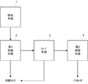
図1を参照して、この実施例のプログラム処理装置は、基本的に次のように構成される。検出手段1は装置の動きを検出する。第1供給手段2は、検出手段1の検知に応答して内部メモリに電源を供給する。ロード手段3は、プロセッサによって実行されるプログラムを第1供給手段2の供給処理に関連して内部メモリにロードする。第2供給手段4は、ロード手段3のロード処理の後の電源オン操作に応答してプロセッサに電源を供給する。
Referring to FIG. 1, the program processing apparatus of this embodiment is basically configured as follows. The detecting means 1 detects the movement of the apparatus. The
装置の動きが検出されると、内部メモリに電源が供給されるとともに内部メモリにプログラムがロードされる。また、ロードされたプログラムを実行するプロセッサには、ロード処理の後の電源オン操作に応答して電源が供給される。したがって、その後プロセッサによってプログラムが実行される際にプログラムを内部メモリにロードする必要がなく、プログラムが実行可能となるまでの期間を短縮することができる。また、プログラム処理装置の不要な起動に起因する電力の浪費を抑制することができる。
[実施例]
When the movement of the apparatus is detected, power is supplied to the internal memory and a program is loaded into the internal memory. In addition, power is supplied to the processor that executes the loaded program in response to a power-on operation after the loading process. Therefore, when the program is subsequently executed by the processor, it is not necessary to load the program into the internal memory, and the period until the program becomes executable can be shortened. Further, it is possible to suppress waste of electric power due to unnecessary activation of the program processing device.
[Example]
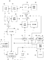
図2を参照して、この実施例のディジタルカメラ10は、電源回路46を含む。電源回路46は、互いに異なる電圧値を各々が示す複数の直流電源をバッテリ48に基づいて生成する。
Referring to FIG. 2, the
生成された複数の直流電源の一部はサブCPU44およびジャイロセンサ56に直接的に与えられ、生成された複数の直流電源の他の一部は主電源スイッチ50,第1メモリ電源スイッチ52,および第2メモリ電源スイッチ54を介してシステム全体に与えられる。したがって、サブCPU44およびジャイロセンサ56は常時起動されるのに対して、システム全体を構成する要素の起動/停止は以下のように制御される。システム全体のうち、メモリ制御回路30およびSDRAM32は第1メモリ電源スイッチ52のオン/オフに応答して起動/停止され、フラッシュメモリ42は第2メモリ電源スイッチ54のオン/オフに応答して起動/停止される。システム全体を構成する他の要素は、主電源スイッチ50のオン/オフに応答して起動/停止される。
A part of the generated plurality of DC power supplies is directly given to the
フラッシュメモリ42は、ディジタルカメラ10のファームウェアおよびファームウェアの実行に必要な初期設定値を保持する。
The
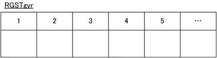
ジャイロセンサ56は、ディジタルカメラ10に動きが発生したか否かを検知し、動きの発生が検知されると検知された動きを表す動きベクトルを出力する。ジャイロセンサ56から出力された動きベクトルは、サブCPU44によって取り込まれ、図3に示すレジスタRGSTgyrに登録される。レジスタRGSTgyrには複数回の動き発生にそれぞれ対応する複数の動きベクトルが保持される。なお、ジャイロセンサ56によって検知される動きには、振動,移動,回転,および回動等が含まれる。
The
ディジタルカメラ10の操作者は通常、ディジタルカメラ10を手に取って電源オン操作を行う。したがって、ジャイロセンサ56から動きベクトルが出力されたとき、ディジタルカメラ10が電源オン操作のために操作者によって動かされたと判断される。このとき、サブCPU44は、第1メモリ電源スイッチ52および第2メモリ電源スイッチ54をそれぞれ制御して、メモリ制御回路30,SDRAM32,およびフラッシュメモリ42を起動する。
An operator of the
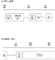
サブCPU44は次に、ディジタルカメラ10のファームウェアおよびファームウェアの実行に必要な初期設定値をフラッシュメモリ42からSDRAM32に転送する(図4(A)参照)。転送が完了するとサブCPU44は、タイマ44tのリセット&スタートを実行する。タイマ値は例えば5秒とする。
Next, the
タイマ44tにタイムアウトが発生する前にキー入力装置28上の電源ボタン28aによって電源オン操作が行われると、システム全体のうち起動されていなかった残りの要素を、サブCPU44は主電源スイッチ50を制御して起動する。起動されたメインCPU26は、SDRAM32に保持されたファームウェアを実行する。
If the power-on operation is performed by the
なお、ディジタルカメラ10が動かされることなく電源オン操作が行われた場合、動きベクトルがジャイロセンサ56から出力されず、電源オン操作の前に上述の転送処理が実行されない。この場合、SDRAM32およびフラッシュメモリ42を含むシステム全体の起動後に、サブCPU44は、ディジタルカメラ10のファームウェアおよびファームウェアの実行に必要な初期設定値をフラッシュメモリ42からSDRAM32に転送する。このようにしてSDRAM32に保持されたファームウェアは、起動されたメインCPU26によって実行される。
When the power-on operation is performed without moving the
ファームウェアの実行に従って、メインCPU26においてメインタスクが起動される。起動されたメインタスクの下でメインCPU26は、キー入力装置28に設けられたモード変更ボタン28mdの状態(つまり現時点の動作モード)を判別し、撮像モードに対応して撮像タスクを起動する一方、再生モードに対応して再生タスクを起動する。
A main task is activated in the
撮像タスクが起動されるとメインCPU26は、動画取り込み処理のためにドライバ18を起動する。ドライバ18は、周期的に発生する垂直同期信号Vsyncに応答して、撮像面を露光し、撮像面で生成された電荷をラスタ走査態様で読み出す。イメージセンサ16からは、被写界を表す生画像データが繰り返し出力される。
When the imaging task is activated, the
信号処理回路20は、イメージセンサ16から出力された生画像データに白バランス調整,色分離,YUV変換などの処理を施し、これによって作成されたYUV形式の画像データをメモリ制御回路30を通してSDRAM32に書き込む。LCDドライバ34は、SDRAM32に格納された画像データをメモリ制御回路30を通して読み出し、読み出された画像データに基づいてLCDモニタ36を駆動する。この結果、被写界のリアルタイム動画像(スルー画像)がLCDモニタ36に表示される。
The
シャッタボタン28shが全押しされると、メインCPU26は撮像タスクの下で静止画取り込み処理および記録処理を実行する。静止画取り込み処理によって取り込まれた1フレームの画像データは、記録処理に関連して起動したI/F38によってファイル形式で記録媒体40に記録される。
When the shutter button 28sh is fully pressed, the
再生タスクが起動されるとメインCPU26は、再生タスクの下で記録媒体40に記録された最新の画像ファイルを再生画像ファイルとして指定し、指定画像ファイルに注目した再生処理が実行される。この結果、指定画像ファイルの画像データに対応する光学像がLCDモニタ36に表示される。
When the reproduction task is activated, the
操作者によるキー入力装置28の操作によって、メインCPU26は、後続の画像ファイルまたは先行する画像ファイルを再生画像ファイルとして指定する。指定画像ファイルは上述と同様の再生処理を施され、この結果、LCDモニタ36の表示が更新される。
By the operation of the
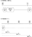
図4(B)を参照して、電源ボタン28aによって電源オフ操作が行われたときは、メインCPU26は実行中のタスクを終了し、SDRAM32にセルフリフレッシュ命令を発行する。SDRAM32は、自らの内部カウンタを用いたリフレッシュの実行を開始する。システム全体のうちメモリ制御回路30およびSDRAM32を除いた一部は、サブCPU44による主電源スイッチ50および第2メモリ電源スイッチ54の制御に従って停止される。
Referring to FIG. 4B, when the power-off operation is performed by the
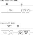
SDRAM32によるセルフリフレッシュは、既定期間内において繰り返し実行される。既定期間は例えば1時間とする。セルフリフレッシュの実行期間内は、ファームウェアおよびファームウェアの実行に必要な初期設定値がSDRAM32に保持されている。したがって、SDRAM32のセルフリフレッシュの実行期間内にジャイロセンサ56から動きベクトルが出力された場合、サブCPU44は上述の転送処理を実行しない(図4(B)参照)。また、図5(A)を参照して、SDRAM32のセルフリフレッシュの実行期間内に電源ボタン28aによって電源オン操作が行われた場合、上述の転送処理が実行されることなく、システム全体のうち起動されていなかった残りの要素が起動され、メインCPU26においてファームウェアが実行される。
Self refresh by the SDRAM 32 is repeatedly executed within a predetermined period. The predetermined period is, for example, 1 hour. During the self-refresh execution period, the SDRAM 32 holds initial setting values necessary for executing the firmware. Therefore, if a motion vector is output from the
図5(B)を参照して、SDRAM32によるセルフリフレッシュの実行期間が終了すると、サブCPU44は、第1メモリ電源スイッチ52を制御してメモリ制御回路30およびSDRAM32を停止する。SDRAM32の停止に従って、ファームウェアおよびファームウェアの実行に必要な初期設定値は、SDRAM32から消失する。したがって、SDRAM32のセルフリフレッシュの実行期間終了後にジャイロセンサ56から動きベクトルが出力された場合、上述の通りサブCPU44は、SDRAM32およびフラッシュメモリ42を起動する。サブCPU44は次に、ファームウェアおよびファームウェアの実行に必要な初期設定値をフラッシュメモリ42からSDRAM32に転送し、タイマ44tのリセット&スタートを実行する。タイマ44tにタイムアウトが発生する前にキー入力装置28上の電源ボタン28aによって電源オン操作が行われると、システム全体のうち起動されていなかった残りの要素が起動され、メインCPU26においてファームウェアが実行される(図4(A)参照)。
Referring to FIG. 5B, when the execution period of self-refreshing by SDRAM 32 ends,
電源ボタン28aによって電源オン操作が行われることなくタイマ44tにタイムアウトが発生したとき、ジャイロセンサ56によって検知されたディジタルカメラ10の動きは、電源オン操作のためではないものと判断される。したがって、サブCPU44は、第1メモリ電源スイッチ52および第2メモリ電源スイッチ54をそれぞれ制御してメモリ制御回路30,SDRAM32,およびフラッシュメモリ42を停止する(図6(A)参照)。
When a time-out occurs in the
このように、電源オン操作が行われるか否かに関わらず、ディジタルカメラ10の動き発生に従って動きベクトルがジャイロセンサ56から出力される。例えば、ディジタルカメラ10が操作者によって携帯されたとき、乗り物による移動および操作者の歩行等によって繰り返される振動の発生に従って、ジャイロセンサ56は、ディジタルカメラ10の動きを検知する毎に動きベクトルを出力する。このような周期的な振動による動きベクトルの出力パターンは、1または2以上の既定動きパターンとして準備される。
As described above, regardless of whether the power-on operation is performed, the motion vector is output from the
レジスタRGSTgyrに動きベクトルが新たに登録されると、サブCPU44は、レジスタRGSTgyrに登録された複数の動きベクトルの発生パターンを1または2以上の既定動きパターンの各々と照合する。この結果、動きベクトルの発生パターンがいずれかの既定動きパターンと一致したとき、サブCPU44は、電源オン操作が行われないものと判断し、上述の転送処理を実行しない(図6(B)参照)。
When a motion vector is newly registered in the register RGSTgyr, the
レジスタRGSTgyrには複数回の動き発生にそれぞれ対応する複数の動きベクトルが保持されるが、最新の動きベクトルの登録時から遡ってパターン照合に必要な期間内に登録された1または2以上の動きベクトルが、確保されていればよい。動きベクトルを確保する期間は例えば15秒間とする。 The register RGSTgyr holds a plurality of motion vectors respectively corresponding to a plurality of motion occurrences, but one or more motions registered within a period required for pattern matching retroactively from the registration of the latest motion vector. The vector only needs to be secured. The period for securing the motion vector is, for example, 15 seconds.
また、上述の転送処理を制限するためのロックスイッチ28bがキー入力装置28に設けられている。操作者の操作によってロックスイッチ28bの状態がロックまたはアンロックのいずれかに設定される。動きベクトルがジャイロセンサ56から出力されたとき、ロックスイッチ28bがアンロック状態の場合に限り転送処理が実行され、ロックスイッチ28bがロック状態の場合は転送処理が実行されない。なお、ロックスイッチ28bがロック状態の場合、ジャイロセンサ56への電源の供給を停止するようにしてもよい。
Further, the
サブCPU44は、図7〜図10に示すフロー図に従う処理を実行する。また、メインCPU26は、図11に示すメインタスクを含む複数のタスクを並列的に実行する。なお、メインタスクを含むメインCPU26で実行されるタスクに対応する制御プログラムは、上述のファームウェアとしてフラッシュメモリ42に記憶される。
The
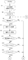
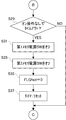
図7を参照して、ステップS1ではタイマ44tの値を“5秒”に初期化し、ステップS3ではフラグFLGfwdに“0”を初期設定する。ジャイロセンサ56による動きベクトルの出力に従って、ステップS5ではディジタルカメラ10に動きが発生したか否かを判別する。判別結果がNOであればステップS29に進む一方、判別結果がYESであればステップS7に進む。
Referring to FIG. 7, in step S1, the value of
ステップS7では、ジャイロセンサ56から出力された動きベクトルをレジスタRGSTgyrに登録する。ステップS9では、レジスタRGSTgyrに登録された複数の動きベクトルの発生パターンを1または2以上の既定動きパターンの各々と照合する。
In step S7, the motion vector output from the
ステップS11では、ステップS9の照合処理の結果、動きベクトルの発生パターンがいずれかの既定動きパターンと一致したか否かを判別する。判別結果がYESであれば、電源オン操作が行われないものと判断してステップS29に進む。一方、判別結果がNOであればステップS13に進む。 In step S11, it is determined whether or not the motion vector generation pattern matches any of the predetermined motion patterns as a result of the collation process in step S9. If the determination result is YES, it is determined that the power-on operation is not performed, and the process proceeds to step S29. On the other hand, if a determination result is NO, it will progress to Step S13.
ステップS13ではロックスイッチ28bがアンロック状態であるか否かを判別し、判別結果がNOであればステップS29に進む一方、判別結果がYESであればステップS15に進む。ステップS15では、フラグFLGfwdに“0”が設定されているか否かを判別し、判別結果がNOであればステップS29に進む一方、判別結果がYESであればステップS17に進む。
In step S13, it is determined whether or not the
ステップS17では第1メモリ電源スイッチ52を制御してメモリ制御回路30およびSDRAM32を起動し、ステップS19では第2メモリ電源スイッチ54を制御してフラッシュメモリ42を起動する。
In step S17, the first
ステップS21では、ディジタルカメラ10のファームウェアの実行に必要な初期設定値をフラッシュメモリ42からSDRAM32に転送する。ステップS23では、ディジタルカメラ10のファームウェアをフラッシュメモリ42からSDRAM32に転送する。
In step S 21, initial setting values necessary for executing the firmware of the
ステップS25ではフラグFLGfwdに“1”を設定し、ステップS27ではタイマ44tのリセット&スタートを実行する。ステップS29では、電源オン操作が行われることなくタイマ44tにタイムアウトが発生したか否かを判別し、判別結果がNOであればステップS39に進む一方、判別結果がYESであればステップS31〜ステップS37の処理を経てステップS39に進む。
In step S25, the flag FLGfwd is set to “1”. In step S27, the
ステップS31では第1メモリ電源スイッチ52を制御してメモリ制御回路30およびSDRAM32を停止し、ステップS33では第2メモリ電源スイッチ54を制御してフラッシュメモリ42を停止する。ステップS35ではフラグFLGfwdに“0”を設定し、ステップS37ではタイマ44tのリセットを実行する。
In step S31, the first
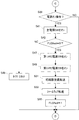
ステップS39では電源ボタン28aによって電源オン操作が行われたか否かを判別し、判別結果がNOであればステップS57に進む一方、判別結果がYESであればステップS41で主電源スイッチ50をオンにする。
In step S39, it is determined whether or not a power-on operation has been performed by the
ステップS43ではフラグFLGfwdに“0”が設定されているか否かを判別し、判別結果がNOであればステップS45の処理を経てステップS57に進む一方、判別結果がYESであればステップS47〜ステップS55の処理を経てステップS57に進む。ステップS45ではタイマ44tのリセットを実行する。
In step S43, it is determined whether or not “0” is set in the flag FLGfwd. If the determination result is NO, the process proceeds to step S57 through the process of step S45, whereas if the determination result is YES, the process proceeds from step S47 to step S47. It progresses to step S57 through the process of S55. In step S45, the
ステップS47では第1メモリ電源スイッチ52を制御してメモリ制御回路30およびSDRAM32を起動し、ステップS49では第2メモリ電源スイッチ54を制御してフラッシュメモリ42を起動する。
In step S47, the first
ステップS51では、ディジタルカメラ10のファームウェアの実行に必要な初期設定値をフラッシュメモリ42からSDRAM32に転送する。ステップS53では、ディジタルカメラ10のファームウェアをフラッシュメモリ42からSDRAM32に転送する。ステップS55ではフラグFLGfwdに“1”を設定する。
In step S51, initial setting values necessary for executing the firmware of the
ステップS57では電源ボタン28aによって電源オフ操作が行われたか否かを判別し、判別結果がNOであればステップS63に進む一方、判別結果がYESであればステップS59〜ステップS61の処理を経てステップS63に進む。
In step S57, it is determined whether or not a power-off operation has been performed by the
ステップS59およびステップS61では主電源スイッチ50および第2メモリ電源スイッチ54をそれぞれ制御して、システム全体のうちメモリ制御回路30およびSDRAM32を除いた一部を停止する。SDRAM32は、自らの内部カウンタを用いたリフレッシュの実行を開始する。
In steps S59 and S61, the
ステップS63ではSDRAM32のセルフリフレッシュの実行期間が終了したか否かを判別し、判別結果がNOであればステップS5に戻る一方、判別結果がYESであればステップS65〜ステップS67の処理を経てステップS5に戻る。ステップS65では第1メモリ電源スイッチ52を制御してメモリ制御回路30およびSDRAM32を停止し、ステップS67ではフラグFLGfwdに“0”を設定する。
In step S63, it is determined whether or not the execution period of the self refresh of the SDRAM 32 has ended. If the determination result is NO, the process returns to step S5. If the determination result is YES, the process proceeds from step S65 to step S67. Return to S5. In step S65, the first
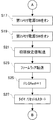
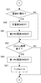
図12を参照して、ステップS71では現時点の動作モードが撮像モードであるか否かを判別し、ステップS75では現時点の動作モードが再生モードであるか否かを判別する。ステップS71の判別結果がYESであれば、ステップS73で撮像タスクを起動する。ステップS75の判別結果がYESであれば、ステップS77で再生タスクを起動する。ステップS71の判別結果およびステップS75の判別結果のいずれもがNOであれば、ステップS79でその他の処理を実行する。 Referring to FIG. 12, in step S71, it is determined whether or not the current operation mode is the imaging mode, and in step S75, it is determined whether or not the current operation mode is the reproduction mode. If the determination result in step S71 is YES, the imaging task is activated in step S73. If the decision result in the step S75 is YES, a reproduction task is activated in a step S77. If both the determination result in step S71 and the determination result in step S75 are NO, other processing is executed in step S79.
ステップS73,ステップS77,またはステップS79の処理が完了すると、モード変更ボタン28mdが操作されたか否かをステップS81で繰り返し判別する。判別結果がNOからYESに更新されると、起動中のタスクをステップS83で停止し、その後にステップS71に戻る。 When the process of step S73, step S77, or step S79 is completed, it is repeatedly determined in step S81 whether or not the mode change button 28md has been operated. When the determination result is updated from NO to YES, the activated task is stopped in step S83, and thereafter, the process returns to step S71.
以上の説明から分かるように、ジャイロセンサ56はディジタルカメラ10の動きを検出する。第1メモリ電源スイッチ52,第2メモリ電源スイッチ54,およびサブCPU44は、ジャイロセンサ56の検知に応答してSDRAM32に電源を供給する。サブCPU44は、メインCPU26によって実行されるプログラムを第1メモリ電源スイッチ52,第2メモリ電源スイッチ54,およびサブCPU44の供給処理に関連してSDRAM32にロードする。主電源スイッチ50およびサブCPU44は、サブCPU44のロード処理の後の電源オン操作に応答してメインCPU26に電源を供給する。
As can be understood from the above description, the
動きが検出されると、内部メモリに電源が供給されるとともに内部メモリにプログラムがロードされる。また、ロードされたプログラムを実行するプロセッサには、ロード処理の後の電源オン操作に応答して電源が供給される。したがって、その後プロセッサによってプログラムが実行される際にプログラムを内部メモリにロードする必要がなく、プログラムが実行可能となるまでの期間を短縮することができる。また、プログラム処理装置の不要な起動に起因する電力の浪費を抑制することができる。 When motion is detected, power is supplied to the internal memory and a program is loaded into the internal memory. In addition, power is supplied to the processor that executes the loaded program in response to a power-on operation after the loading process. Therefore, when the program is subsequently executed by the processor, it is not necessary to load the program into the internal memory, and the period until the program becomes executable can be shortened. Further, it is possible to suppress waste of electric power due to unnecessary activation of the program processing device.
なお、この実施例では、ディジタルカメラ10のファームウェア等をフラッシュメモリ42からSDRAM32に転送するようにした。しかし、ディジタルカメラ10のファームウェア等が記録媒体40に保持されるようにし、記録媒体40からSDRAM32に転送するようにしてもよい。
In this embodiment, the firmware of the
また、この実施例では、電源オン操作が行われることなくタイマ44tにタイムアウトが発生したとき、SDRAM32およびフラッシュメモリ42を停止するようにした。しかし、フラッシュメモリ42の停止は、ファームウェア等の転送処理の完了後直ちに実行するようにしてもよい。
In this embodiment, the SDRAM 32 and the
また、この実施例では、ディジタルスチルカメラを用いて説明したが、本発明は、ディジタルビデオカメラ,パーソナルコンピュータ,携帯電話端末,スマートフォン,またはディジタルオーディオプレーヤーなどの揮発性メモリが用いられる他の機器にも適用することができる。 In this embodiment, the digital still camera has been described. However, the present invention is applied to other devices using a volatile memory such as a digital video camera, a personal computer, a mobile phone terminal, a smartphone, or a digital audio player. Can also be applied.
10 … ディジタルカメラ
26 … メインCPU
32 … SDRAM
44 … サブCPU
50 … 主電源スイッチ
52 … 第1メモリ電源スイッチ
54 … 第2メモリ電源スイッチ
56 … ジャイロセンサ
10 ...
32 ... SDRAM
44 ... Sub CPU
50 ...
Claims (10)
前記検出手段の検知に応答して内部メモリに電源を供給する第1供給手段、
プロセッサによって実行されるプログラムを前記第1供給手段の供給処理に関連して前記内部メモリにロードするロード手段、および
前記ロード手段のロード処理の後の電源オン操作に応答して前記プロセッサに前記電源を供給する第2供給手段を備える、プログラム処理装置。 Detecting means for detecting movement of the device;
First supply means for supplying power to the internal memory in response to detection by the detection means;
Load means for loading a program executed by the processor into the internal memory in relation to the supply process of the first supply means; and the power supply to the processor in response to a power-on operation after the load process of the load means A program processing apparatus comprising second supply means for supplying
前記プロセッサ電源停止手段の停止処理から指定期間が経過したとき前記内部メモリへの前記電源の供給を停止する第2メモリ電源停止手段をさらに備える、請求項1ないし3のいずれかに記載のプログラム処理装置。 A processor power supply stopping means for stopping the supply of power to the processor in response to a power-off operation, and the supply of power to the internal memory is stopped when a specified period has elapsed from the stop processing of the processor power supply stop means 4. The program processing apparatus according to claim 1, further comprising second memory power supply stopping means.
前記検出手段の検知に応答して内部メモリに電源を供給する第1供給ステップ、
第2プロセッサによって実行されるプログラムを前記第1供給ステップの供給処理に関連して前記内部メモリにロードするロードステップ、および
前記ロードステップのロード処理の後の電源オン操作に応答して前記第2プロセッサに前記電源を供給する第2供給ステップを実行させるための、プログラム処理プログラム。 A first processor of a program processing device comprising detection means for detecting the movement of the device;
A first supply step of supplying power to the internal memory in response to detection by the detection means;
A load step of loading a program executed by the second processor into the internal memory in relation to the supply process of the first supply step; and A program processing program for causing a processor to execute a second supply step of supplying the power.
前記検出手段の検知に応答して内部メモリに電源を供給する第1供給ステップ、
プロセッサによって実行されるプログラムを前記第1供給ステップの供給処理に関連して前記内部メモリにロードするロードステップ、および
前記ロードステップのロード処理の後の電源オン操作に応答して前記プロセッサに前記電源を供給する第2供給ステップを備える、プログラム処理方法。 A program processing method executed by a program processing device including a detecting unit for detecting movement of the device,
A first supply step of supplying power to the internal memory in response to detection by the detection means;
A load step for loading a program to be executed by a processor into the internal memory in relation to the supply process of the first supply step; and the power supply to the processor in response to a power-on operation after the load process of the load step. A program processing method comprising a second supply step of supplying
Priority Applications (3)
| Application Number | Priority Date | Filing Date | Title |
|---|---|---|---|
| JP2011071743A JP2012208564A (en) | 2011-03-29 | 2011-03-29 | Program processing device |
| CN2012100820213A CN102841670A (en) | 2011-03-29 | 2012-03-26 | Program processing apparatus |
| US13/434,577 US20120254648A1 (en) | 2011-03-29 | 2012-03-29 | Program processing apparatus |
Applications Claiming Priority (1)
| Application Number | Priority Date | Filing Date | Title |
|---|---|---|---|
| JP2011071743A JP2012208564A (en) | 2011-03-29 | 2011-03-29 | Program processing device |
Publications (1)
| Publication Number | Publication Date |
|---|---|
| JP2012208564A true JP2012208564A (en) | 2012-10-25 |
Family
ID=46928933
Family Applications (1)
| Application Number | Title | Priority Date | Filing Date |
|---|---|---|---|
| JP2011071743A Withdrawn JP2012208564A (en) | 2011-03-29 | 2011-03-29 | Program processing device |
Country Status (3)
| Country | Link |
|---|---|
| US (1) | US20120254648A1 (en) |
| JP (1) | JP2012208564A (en) |
| CN (1) | CN102841670A (en) |
Families Citing this family (4)
| Publication number | Priority date | Publication date | Assignee | Title |
|---|---|---|---|---|
| US9600049B2 (en) * | 2013-06-07 | 2017-03-21 | Apple Inc. | Motion fencing |
| CN105824438A (en) * | 2015-08-07 | 2016-08-03 | 维沃移动通信有限公司 | Data distribution method and terminal |
| JP7112060B2 (en) * | 2018-12-26 | 2022-08-03 | ルネサスエレクトロニクス株式会社 | Semiconductor device and its power control method |
| WO2021015794A1 (en) * | 2019-07-25 | 2021-01-28 | Hewlett-Packard Development Company, L.P. | Power supplies to variable performance electronic components |
-
2011
- 2011-03-29 JP JP2011071743A patent/JP2012208564A/en not_active Withdrawn
-
2012
- 2012-03-26 CN CN2012100820213A patent/CN102841670A/en active Pending
- 2012-03-29 US US13/434,577 patent/US20120254648A1/en not_active Abandoned
Also Published As
| Publication number | Publication date |
|---|---|
| US20120254648A1 (en) | 2012-10-04 |
| CN102841670A (en) | 2012-12-26 |
Similar Documents
| Publication | Publication Date | Title |
|---|---|---|
| US7805624B2 (en) | Electronic device, and external device control method using said electronic device | |
| US8176305B2 (en) | Information processing apparatus, activation method, and program | |
| US8117476B2 (en) | Information processing apparatus, startup method and computer program | |
| US8069360B2 (en) | Apparatus, method and computer program for processing information | |
| JP6786797B2 (en) | Information processing equipment, imaging equipment, information processing systems, information processing methods, and programs | |
| JP5590626B2 (en) | Imaging apparatus, imaging method, and program | |
| JP4232121B2 (en) | Information processing apparatus and method, program, and recording medium | |
| JP2014094553A (en) | Information processing apparatus | |
| CN1972384B (en) | Information processing apparatus, imaging apparatus, and information processing method | |
| JP2012208564A (en) | Program processing device | |
| JP2015007890A (en) | Electronic device, control method and program for electronic device | |
| US20120079300A1 (en) | Electronic apparatus | |
| US9742998B2 (en) | Imaging apparatus | |
| WO2020129303A1 (en) | Image-capturing apparatus | |
| JP2008165554A (en) | Information processing apparatus, activation method, and program | |
| CN106713705A (en) | Communication apparatus and control method for the communication apparatus | |
| CN118042272A (en) | Image pickup apparatus, control method of image pickup apparatus, and computer-readable medium | |
| JP2008165553A (en) | Information processing apparatus and method, and program | |
| JP2016175349A (en) | Control device, image formation apparatus, control method and program | |
| JP7039576B2 (en) | Electronics, power management methods, and power management systems | |
| JP5230353B2 (en) | Imaging apparatus and control method thereof | |
| JP2009177612A (en) | Electronic device, camera, and start control method and start control program for electronic device | |
| US20090290846A1 (en) | Method and apparatus for recording image in electronic apparatus | |
| KR100698314B1 (en) | Mobile communication terminal with shooting function and method using the same | |
| JP2008165586A (en) | Information processing apparatus, information processing method, and program |
Legal Events
| Date | Code | Title | Description |
|---|---|---|---|
| A711 | Notification of change in applicant |
Free format text: JAPANESE INTERMEDIATE CODE: A711 Effective date: 20130404 |
|
| RD03 | Notification of appointment of power of attorney |
Free format text: JAPANESE INTERMEDIATE CODE: A7423 Effective date: 20130521 |
|
| A300 | Application deemed to be withdrawn because no request for examination was validly filed |
Free format text: JAPANESE INTERMEDIATE CODE: A300 Effective date: 20140603 |