JP2012208342A5 - - Google Patents
Download PDFInfo
- Publication number
- JP2012208342A5 JP2012208342A5 JP2011074348A JP2011074348A JP2012208342A5 JP 2012208342 A5 JP2012208342 A5 JP 2012208342A5 JP 2011074348 A JP2011074348 A JP 2011074348A JP 2011074348 A JP2011074348 A JP 2011074348A JP 2012208342 A5 JP2012208342 A5 JP 2012208342A5
- Authority
- JP
- Japan
- Prior art keywords
- signal
- ext
- skew
- signal ext
- signal processing
- Prior art date
- Legal status (The legal status is an assumption and is not a legal conclusion. Google has not performed a legal analysis and makes no representation as to the accuracy of the status listed.)
- Pending
Links
Images
Description
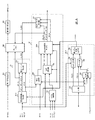
読出制御部22のスキュー補償部221は、信号処理回路を複数用いたマルチチップ構成で映像表示を行う場合、各信号処理回路間で入力映像信号のスキューを生じても、このスキューによる誤動作を防止する。スキュー補償部221は、信号処理回路制御部40から供給された水平同期信号Ext_Hと垂直同期信号Ext_Vとフレーム信号Ext_FLDに基づき、信号処理後の映像信号を各信号処理回路から位相差を少なくして出力できるようにタイミングを調整する。スキュー補償部221は、タイミング調整後の各信号を信号選択部222に出力する。例えば各信号処理回路間でシステムクロックの最大4クロック分のスキューが発生する場合、水平同期信号Ext_Hを8クロック分遅延させる。この場合、遅延後の水平同期信号Ext_Hのタイミングは、最大4クロック分のスキューが発生しても、同じ垂直期間およびフィールド期間のタイミングとなる。したがって、遅延した水平同期信号Ext_Hのエッジで垂直同期信号Ext_Vとフレーム信号Ext_FLDの取り込みを行い、新たな垂直同期信号Ext_Vとフレーム信号Ext_FLDとして出力する。このようにすれば、各信号処理回路間でスキューが発生しても、スキューの影響を防止できる。また、水平同期信号Ext_Hの遅延は、発振器45-Aからのシステムクロック信号SCLKに基づいて行うことで、信号処理回路制御部40から水平同期信号Ext_Hと垂直同期信号Ext_Vとフレーム信号Ext_FLDと共にクロック信号を供給する必要がない。
When the
Priority Applications (5)
| Application Number | Priority Date | Filing Date | Title |
|---|---|---|---|
| JP2011074348A JP2012208342A (en) | 2011-03-30 | 2011-03-30 | Signal processing circuit, signal processing method, and display device |
| TW101109666A TW201301257A (en) | 2011-03-30 | 2012-03-21 | Signal processing circuit, signal processing method, and display apparatus |
| KR1020120029400A KR20120112059A (en) | 2011-03-30 | 2012-03-22 | Signal processing circuit, signal processing method, and display apparatus |
| CN2012100843465A CN102737618A (en) | 2011-03-30 | 2012-03-23 | Signal processing circuit, signal processing method, and display apparatus |
| US13/428,129 US20120249565A1 (en) | 2011-03-30 | 2012-03-23 | Signal processing circuit, signal processing method, and display apparatus |
Applications Claiming Priority (1)
| Application Number | Priority Date | Filing Date | Title |
|---|---|---|---|
| JP2011074348A JP2012208342A (en) | 2011-03-30 | 2011-03-30 | Signal processing circuit, signal processing method, and display device |
Publications (2)
| Publication Number | Publication Date |
|---|---|
| JP2012208342A JP2012208342A (en) | 2012-10-25 |
| JP2012208342A5 true JP2012208342A5 (en) | 2014-04-03 |
Family
ID=46926598
Family Applications (1)
| Application Number | Title | Priority Date | Filing Date |
|---|---|---|---|
| JP2011074348A Pending JP2012208342A (en) | 2011-03-30 | 2011-03-30 | Signal processing circuit, signal processing method, and display device |
Country Status (5)
| Country | Link |
|---|---|
| US (1) | US20120249565A1 (en) |
| JP (1) | JP2012208342A (en) |
| KR (1) | KR20120112059A (en) |
| CN (1) | CN102737618A (en) |
| TW (1) | TW201301257A (en) |
Families Citing this family (8)
| Publication number | Priority date | Publication date | Assignee | Title |
|---|---|---|---|---|
| TWI463432B (en) * | 2012-10-05 | 2014-12-01 | Genesys Logic Inc | Method for processing image data |
| KR101695007B1 (en) * | 2012-12-14 | 2017-01-10 | 한국전자통신연구원 | Apparatus for parallel processing of large-scale video data and method thereof |
| JP6034703B2 (en) * | 2013-01-21 | 2016-11-30 | サターン ライセンシング エルエルシーSaturn Licensing LLC | Conversion circuit, image processing apparatus, and conversion method |
| KR20140112892A (en) * | 2013-03-14 | 2014-09-24 | 삼성디스플레이 주식회사 | Touch Screen Panel and Fabricating Method Thereof |
| JP2015001549A (en) * | 2013-06-13 | 2015-01-05 | ソニー株式会社 | Signal output apparatus, signal output method, and image display apparatus |
| WO2015136571A1 (en) | 2014-03-11 | 2015-09-17 | パナソニック液晶ディスプレイ株式会社 | Display device and driving method therefor |
| KR102631190B1 (en) * | 2016-10-31 | 2024-01-29 | 엘지디스플레이 주식회사 | Display device and its driving method |
| DE112020000617T5 (en) * | 2019-12-17 | 2021-11-04 | Panasonic Intellectual Property Management Co., Ltd. | Display control system, mobile body, display control method, display device, display method and program |
Family Cites Families (13)
| Publication number | Priority date | Publication date | Assignee | Title |
|---|---|---|---|---|
| JP2907988B2 (en) * | 1990-10-05 | 1999-06-21 | 株式会社日立製作所 | Wide television receiver |
| US5841430A (en) * | 1992-01-30 | 1998-11-24 | Icl Personal Systems Oy | Digital video display having analog interface with clock and video signals synchronized to reduce image flicker |
| JPH1055161A (en) * | 1996-08-13 | 1998-02-24 | Fujitsu General Ltd | Pll circuit for digital video processing device |
| WO1998007272A1 (en) * | 1996-08-13 | 1998-02-19 | Fujitsu General Limited | Pll circuit for digital display device |
| US6333750B1 (en) * | 1997-03-12 | 2001-12-25 | Cybex Computer Products Corporation | Multi-sourced video distribution hub |
| US5914757A (en) * | 1997-04-21 | 1999-06-22 | Philips Electronics North America Corporation | Synchronization of multiple video and graphic sources with a display using a slow PLL approach |
| JP3582382B2 (en) * | 1998-11-13 | 2004-10-27 | 株式会社日立製作所 | Display control device for multi-display device, display device, and multi-display device |
| JP2000232649A (en) * | 1998-12-10 | 2000-08-22 | Fujitsu Ltd | Mpeg video decoder and mpeg video decoding method |
| JP2006148765A (en) * | 2004-11-24 | 2006-06-08 | Seiko Epson Corp | Television receiver |
| JP5099406B2 (en) * | 2006-11-14 | 2012-12-19 | ソニー株式会社 | Signal processing circuit and method |
| JP5106893B2 (en) * | 2007-03-20 | 2012-12-26 | 三菱電機株式会社 | Display device |
| JP5335273B2 (en) * | 2008-04-17 | 2013-11-06 | キヤノン株式会社 | Memory control device and memory control method |
| JP2011061323A (en) * | 2009-09-07 | 2011-03-24 | Toshiba Corp | Synchronization signal control circuit and display device |
-
2011
- 2011-03-30 JP JP2011074348A patent/JP2012208342A/en active Pending
-
2012
- 2012-03-21 TW TW101109666A patent/TW201301257A/en unknown
- 2012-03-22 KR KR1020120029400A patent/KR20120112059A/en not_active Application Discontinuation
- 2012-03-23 US US13/428,129 patent/US20120249565A1/en not_active Abandoned
- 2012-03-23 CN CN2012100843465A patent/CN102737618A/en active Pending
Similar Documents
| Publication | Publication Date | Title |
|---|---|---|
| JP2012208342A5 (en) | ||
| US8872557B2 (en) | Data output timing control circuit for semiconductor apparatus | |
| DE602006001964D1 (en) | Synchronization of several operational flight programs | |
| EP2884228A3 (en) | Detection device, sensor, electronic apparatus and moving object | |
| TW201130229A (en) | Delay locked loop and method of driving delay locked loop | |
| JP2016522499A5 (en) | ||
| WO2012121892A3 (en) | Delay circuitry | |
| MX2016013399A (en) | Circuit for generating accurate clock phase dignals for a high-speed serializer/deserializere. | |
| EP2592752A3 (en) | Duty cycle distortion correction circuitry | |
| ATE398892T1 (en) | SYNCHRONIZING AUDIO WITH DELAYED VIDEO | |
| TW200609899A (en) | Image signal processing apparatus and phase synchronization method | |
| WO2010135428A3 (en) | Associating data for events occurring in software threads with synchronized clock cycle counters | |
| SG11201803662SA (en) | Method for synchronising data converters by means of a signal transmitted from one to the next | |
| JP2010273187A5 (en) | PLL circuit | |
| JP2017517077A5 (en) | ||
| ATE470936T1 (en) | DIGITAL DATA BUFFER | |
| WO2013052186A3 (en) | Jitter suppression in type i delay-locked loops | |
| JP2005039829A5 (en) | ||
| TW200627930A (en) | Frame-based phase-locked display controller and method thereof | |
| JP6351542B2 (en) | Circuit board and display device | |
| KR20130044976A (en) | Apparatus for synchronizing stereocamera, stereocamera and method for synchronizing stereocamera | |
| EP3895319A4 (en) | Phase-locked loop (pll) with direct feedforward circuit | |
| US8723570B2 (en) | Delay-locked loop and method for a delay-locked loop generating an application clock | |
| JP2016224089A5 (en) | ||
| JP2012175271A5 (en) |