JP2012204660A - Photovoltaic device, manufacturing method thereof, and photovoltaic module - Google Patents
Photovoltaic device, manufacturing method thereof, and photovoltaic module Download PDFInfo
- Publication number
- JP2012204660A JP2012204660A JP2011068592A JP2011068592A JP2012204660A JP 2012204660 A JP2012204660 A JP 2012204660A JP 2011068592 A JP2011068592 A JP 2011068592A JP 2011068592 A JP2011068592 A JP 2011068592A JP 2012204660 A JP2012204660 A JP 2012204660A
- Authority
- JP
- Japan
- Prior art keywords
- diffusion layer
- single crystal
- silicon substrate
- crystal silicon
- surface side
- Prior art date
- Legal status (The legal status is an assumption and is not a legal conclusion. Google has not performed a legal analysis and makes no representation as to the accuracy of the status listed.)
- Granted
Links
Images


Classifications
-
- Y—GENERAL TAGGING OF NEW TECHNOLOGICAL DEVELOPMENTS; GENERAL TAGGING OF CROSS-SECTIONAL TECHNOLOGIES SPANNING OVER SEVERAL SECTIONS OF THE IPC; TECHNICAL SUBJECTS COVERED BY FORMER USPC CROSS-REFERENCE ART COLLECTIONS [XRACs] AND DIGESTS
- Y02—TECHNOLOGIES OR APPLICATIONS FOR MITIGATION OR ADAPTATION AGAINST CLIMATE CHANGE
- Y02E—REDUCTION OF GREENHOUSE GAS [GHG] EMISSIONS, RELATED TO ENERGY GENERATION, TRANSMISSION OR DISTRIBUTION
- Y02E10/00—Energy generation through renewable energy sources
- Y02E10/50—Photovoltaic [PV] energy
Abstract
Description
本発明は、光起電力装置およびその製造方法、光起電力モジュールに関するものである。 The present invention relates to a photovoltaic device, a manufacturing method thereof, and a photovoltaic module.
太陽電池等の光起電力装置の性能向上には、太陽電池を構成する基板内部に太陽光を効率良く取り込むことが大切である。このため、光入射側の基板表面にテクスチャ加工を施し、基板表面で一度反射した光を再度基板表面に入射させることで、より多くの太陽光を基板内部に取り込み、光電変換効率の向上を図っている。ここでテクスチャ加工とは、基板表面に意図的に数十nm〜数十μmの寸法の微細凹凸を形成する加工のことである。 In order to improve the performance of photovoltaic devices such as solar cells, it is important to efficiently incorporate sunlight into the substrate constituting the solar cells. For this reason, texture processing is performed on the substrate surface on the light incident side, and light once reflected on the substrate surface is incident again on the substrate surface, so that more sunlight is taken into the substrate and the photoelectric conversion efficiency is improved. ing. Here, the texture processing is processing for intentionally forming fine irregularities having dimensions of several tens of nanometers to several tens of micrometers on the substrate surface.
太陽電池用の基板にテクスチャ形成を行う方法として、基板が単結晶基板の場合には、エッチング速度に結晶方位依存性を有する水酸化ナトリウムや水酸化カリウム等のアルカリ水溶液による異方性エッチングが広く用いられる。たとえば、(100)基板表面に対してこの異方性エッチングを行うと、(111)面が露出したピラミッド状のテクスチャが基板表面に形成される。 As a method of texture formation on a substrate for solar cells, when the substrate is a single crystal substrate, anisotropic etching with an aqueous alkali solution such as sodium hydroxide or potassium hydroxide having a crystal orientation dependence on the etching rate is widely used. Used. For example, when this anisotropic etching is performed on the (100) substrate surface, a pyramidal texture with the (111) plane exposed is formed on the substrate surface.
また、単結晶基板にテクスチャを形成する場合、エッチングマスクを利用すると理想的な逆ピラミッドテクスチャを基板表面に形成することができ、写真製版法等によるエッチングマスクを用いた方法が実用化されている。しかし、写真製版法はプロセスコストが高く、また大型の基板には適用しにくいという欠点があった。 When a texture is formed on a single crystal substrate, an ideal inverted pyramid texture can be formed on the surface of the substrate by using an etching mask, and a method using an etching mask by a photoengraving method has been put into practical use. . However, the photoengraving method has drawbacks that the process cost is high and it is difficult to apply to a large substrate.
そこで、写真製版に替わるエッチングマスクの形成方法として、たとえば、シリコン基板の表面に開口部を有するエッチングマスク膜を形成し、このマスク膜表面に対してブラスト加工を実施することでマスク開口部に凹部からなるテクスチャを形成する方法が提案されている(たとえば、特許文献1参照)。 Therefore, as a method for forming an etching mask that replaces photoengraving, for example, an etching mask film having an opening is formed on the surface of a silicon substrate, and a concave portion is formed in the mask opening by blasting the surface of the mask film. There has been proposed a method of forming a texture consisting of (see, for example, Patent Document 1).
また、シリコン基板の表面にエッチングマスクを形成し、このマスク表面に対してブラスト加工を実施することでマスク表面に開口部を形成し、引き続きエッチング加工を実施することでテクスチャを形成する方法を本発明者らは提案している(たとえば、特許文献2参照)。 In addition, the method of forming an etching mask on the surface of the silicon substrate, blasting the mask surface to form an opening in the mask surface, and subsequently performing the etching process to form a texture. Inventors have proposed (for example, refer patent document 2).
一方、光電変換効率を高めるための太陽電池の構造として、受光面側電極直下の不純物濃度に対して、基板の受光面側におけるこれ以外の領域の不純物濃度を低くした選択エミッタ構造がある。選択エミッタ構造では、受光面側電極直下の不純物濃度が高いため、電極とシリコン基板との接触抵抗を低減できる。また、電極部分以外では不純物濃度が低いため、太陽電池の短波長光側の量子効率を良くすることができる。 On the other hand, as a solar cell structure for increasing the photoelectric conversion efficiency, there is a selective emitter structure in which the impurity concentration in the other region on the light receiving surface side of the substrate is made lower than the impurity concentration just below the light receiving surface side electrode. In the selective emitter structure, since the impurity concentration directly under the light receiving surface side electrode is high, the contact resistance between the electrode and the silicon substrate can be reduced. Further, since the impurity concentration is low except for the electrode portion, the quantum efficiency on the short wavelength light side of the solar cell can be improved.
このような選択エミッタ構造を形成するためには、たとえば酸化シリコン膜を形成した基板の受光面側にレジストパターンを形成した後、レジストパターンの開口部の酸化シリコン膜を除去して、受光面側電極に対応した開口部を酸化シリコン膜に形成する。その後、不純物を拡散することにより、酸化シリコン膜の開口部に高濃度の拡散層が形成され、他の部分に低濃度の拡散層が形成される。そして、高濃度の拡散層に合わせて電極ペーストが印刷された後、電極ペーストの焼成が行われて受光面側電極が形成される(たとえば、特許文献3参照)。 In order to form such a selective emitter structure, for example, after forming a resist pattern on the light-receiving surface side of the substrate on which the silicon oxide film is formed, the silicon oxide film at the opening of the resist pattern is removed, and the light-receiving surface side Openings corresponding to the electrodes are formed in the silicon oxide film. Thereafter, by diffusing impurities, a high concentration diffusion layer is formed in the opening of the silicon oxide film, and a low concentration diffusion layer is formed in the other portion. And after electrode paste is printed according to a high concentration diffused layer, baking of electrode paste is performed and a light-receiving surface side electrode is formed (for example, refer to patent documents 3).
しかしながら、上記従来の技術によれば、選択エミッタ構造を形成するためにレジストマスクの印刷工程が必要となるため工程が複雑になる、という問題があった。 However, according to the above conventional technique, there is a problem that the process becomes complicated because a resist mask printing process is required to form the selective emitter structure.
また、上記従来の技術によれば、電極印刷時に高濃度の拡散層を形成した領域に位置合わせを行う必要があり工程に負荷が掛かる、という問題を有する。 Further, according to the above conventional technique, there is a problem that it is necessary to perform alignment in a region where a high-concentration diffusion layer is formed during electrode printing, which places a burden on the process.
本発明は、上記に鑑みてなされたものであって、受光面を高抵抗化しつつ受光面側電極の接続抵抗を低減可能な選択エミッタ構造に類似の拡散層構造を有し、光電変換効率に優れた光起電力装置およびその製造方法、光起電力モジュールを得ることを目的とする。 The present invention has been made in view of the above, and has a diffusion layer structure similar to a selective emitter structure capable of reducing the connection resistance of the light-receiving surface side electrode while increasing the resistance of the light-receiving surface, and improving the photoelectric conversion efficiency. It is an object of the present invention to obtain an excellent photovoltaic device, a manufacturing method thereof, and a photovoltaic module.
上述した課題を解決し、目的を達成するために、本発明にかかる光起電力装置は、一面側に凹凸形状が形成された第1導電型の単結晶シリコン基板と、前記単結晶シリコン基板の一面側の全面において前記凹凸形状の凸部の頂部に分散配置され、第2導電型の不純物元素が第1の濃度で拡散した複数の第1の拡散層と、前記単結晶シリコン基板の一面側において前記第1の拡散層以外の領域に形成され、前記第2導電型の不純物元素が前記第1の濃度よりも低い第2の濃度で拡散した第2の拡散層と、前記第1の拡散層に電気的に接続して前記単結晶シリコン基板の一面側に形成された受光面側電極と、前記単結晶シリコン基板の他面側に形成された裏面側電極と、を備えることを特徴とする。 In order to solve the above-described problems and achieve the object, a photovoltaic device according to the present invention includes a first-conductivity-type single-crystal silicon substrate having a concavo-convex shape formed on one side, and the single-crystal silicon substrate. A plurality of first diffusion layers which are dispersedly arranged on tops of the concavo-convex convex portions on the entire surface of the one surface side and in which a second conductivity type impurity element diffuses at a first concentration; and one surface side of the single crystal silicon substrate A second diffusion layer formed in a region other than the first diffusion layer, wherein the second conductivity type impurity element is diffused at a second concentration lower than the first concentration, and the first diffusion A light receiving surface side electrode electrically connected to the layer and formed on one surface side of the single crystal silicon substrate; and a back surface side electrode formed on the other surface side of the single crystal silicon substrate. To do.
本発明によれば、受光面を高抵抗化しつつ受光面側電極の接続抵抗を低減可能な選択エミッタ構造に類似の拡散層構造を有し、光電変換効率に優れた光起電力装置が容易に得られる、という効果を奏する。 According to the present invention, a photovoltaic device having a diffusion layer structure similar to a selective emitter structure capable of reducing the connection resistance of the light receiving surface side electrode while increasing the resistance of the light receiving surface, and having excellent photoelectric conversion efficiency can be easily obtained. The effect is obtained.
以下に、本発明にかかる光起電力装置およびその製造方法、光起電力モジュールの実施の形態を図面に基づいて詳細に説明する。なお、本発明は以下の記述に限定されるものではなく、本発明の要旨を逸脱しない範囲において適宜変更可能である。また、以下に示す図面においては、理解の容易のため、各部材の縮尺が実際とは異なる場合がある。各図面間においても同様である。また、平面図であっても、図面を見易くするためにハッチングを付す場合がある。 Embodiments of a photovoltaic device, a manufacturing method thereof, and a photovoltaic module according to the present invention will be described below in detail with reference to the drawings. In addition, this invention is not limited to the following description, In the range which does not deviate from the summary of this invention, it can change suitably. In the drawings shown below, the scale of each member may be different from the actual scale for easy understanding. The same applies between the drawings. Further, even a plan view may be hatched to make the drawing easy to see.
実施の形態
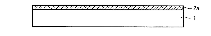
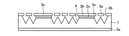
図1−1〜図1−9は、本発明の実施の形態にかかる光起電力装置の製造方法を説明するための要部断面図である。以下、図1−1〜図1−9を参照して本実施の形態にかかる光起電力装置の製造方法を説明する。まず、第1の工程では、単結晶シリコン基板1(以下、基板1と呼ぶ場合がある)の一面側の表面に不純物を拡散して第1の不純物拡散層2a(以下、第1の拡散層2aと呼ぶ)を形成する(図1−1)。
Embodiment FIGS. 1-1 to 1-9 are cross-sectional views of relevant parts for explaining a method of manufacturing a photovoltaic device according to an embodiment of the present invention. Hereinafter, a method for manufacturing the photovoltaic device according to the present embodiment will be described with reference to FIGS. First, in the first step, the first
本実施の形態における単結晶シリコン基板1は、民生用太陽電池向けとして多く使用されているものであり、単結晶シリコンインゴットからマルチワイヤーソーでスライスした後に、酸またはアルカリ溶液を用いたウエットエッチングでスライス時のダメージを除去したものである。たとえばダメージ除去後の基板1の厚みは200μm、寸法は15cm角とされる。なお、基板1の寸法はこれに限定されるものではなく、適宜変更可能である。
The single
また、基板1の極性は、p型およびn型のうちのどちらでもよく、第1の拡散層2aとして基板1の極性の逆の型の拡散層を形成することでpn接合を形成する。第1の拡散層2aがn型の場合はリン(P)を、第1の拡散層2aがp型の場合はボロン(B)を拡散するのが一般的である。
The polarity of the
本実施の形態では、一例として、比抵抗が1Ωcm〜3Ωcmのp型の単結晶シリコン基板1を使用する。第1の拡散層2aは、n型不純物拡散層であり、第1の濃度でリン(P)が拡散された高濃度拡散層(低抵抗領域)である。基板1を熱拡散路に投入し、オキシ塩化リン(POCl3)を用いたリン(P)の熱拡散により、たとえばシート抵抗が20Ω/□〜40Ω/□の第1の拡散層2aを形成する。なお、この第1の拡散層2aのシート抵抗は、後述する第2の拡散層5の形成後の値である。
In the present embodiment, as an example, a p-type single
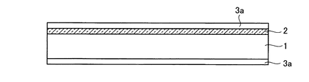
第2の工程では、第1の拡散層2aの表面に保護膜3aを被着する(図1−2)。保護膜としては、800℃〜1000℃の温度で酸化処理を行う熱酸化法により形成される熱酸化膜や、常圧化学気相蒸着(Chemical Vapor Deposition:CVD)法により400℃〜700℃程度の温度で形成される低温酸化膜、プラズマCVD法などの化学堆積法やスパッタリング法などの物理堆積法により形成されるシリコン窒化膜等が使用可能である。また、これらの膜を組み合わせて使用してもよい。熱酸化法では基板1の全面に保護膜が形成されるが、CVD法やスパッタリング法では通常は片面のみの成膜となるため必要に応じて両面への成膜を行う。ただし、基板の裏面側のエッチング保護が不要の場合はこの限りではない。
In the second step, a
第3の工程では、基板1の受光面側(第1の拡散層2a側)に形成された保護膜3aにブラスト加工処理を施して、保護膜3aに開口3bを形成する(図1−3)。すなわち、受光面側(第1の拡散層2a側)に形成された保護膜3aに、ブラスト加工処理により複数の開口3bを開ける。ブラスト加工としては、アルミナ(Al2O3)、炭化シリコン(SiC)やガラス等の砥粒粉体をエアで吹き付ける通常の乾式ブラスト加工や、同じくアルミナ、炭化シリコン(SiC)やガラス等の砥粒粉体を水に分散させたミストをスプレー塗布するウェットブラスト等を使用可能である。
In the third step, the
ブラスト加工処理に使用する砥粒のサイズにより、開口3bの開口穴径と開口ピッチとが変化する。ここでのブラスト加工処理には、たとえば#500〜#3000のサイズの砥粒が使用可能であり、#800〜#2000のサイズの砥粒を用いることが特に好ましい。これにより、後のエッチング工程において底辺長が10μm〜30μm程度のピラミッド形状の粗面構造を形成することができる。なお、粗面構造の形成が両面に必要な場合は、上記ブラスト加工処理を両面に行う必要がある。ここでは、基板1の受光面側のみに粗面構造を形成する場合について説明する。
Depending on the size of the abrasive grains used for the blast processing, the aperture diameter and aperture pitch of the
第4の工程では、開口3bが形成された保護膜3aをマスクとして、基板1の受光面側(第1の拡散層2a側)の一面に対して異方性エッチングを施して、基板1の受光面側(第1の拡散層2a側)の粗面化を行う(図1−4)。異方性エッチングとしては、保護膜3aが耐性を有する条件で、アルカリ水溶液を用いたウエットエッチングを行う。
In the fourth step, anisotropic etching is performed on one surface of the light-receiving surface side (
エッチング液には、シリコンを溶解し、保護膜3aに対する溶解能が小さいものであれば使用可能である。このようなエッチング液としては、たとえばアルカリ水溶液、およびエッチング異方性を付与するイソプロパノール等の添加剤を含むアルカリ水溶液のうちの何れか、またはこれらを組み合わせたものを用いることができる。このようなエッチング液を用いることにより、基板1の表面にランダムピラミッドと呼ばれる凹凸形状からなる粗面形状4を形成することができる。この時のランダムピラミッドのサイズは、先に示した通り、ブラスト加工処理工程で形成される開口3bの開口穴径と開口ピッチで決定される。
Any etching solution may be used as long as it dissolves silicon and has a small dissolving ability with respect to the
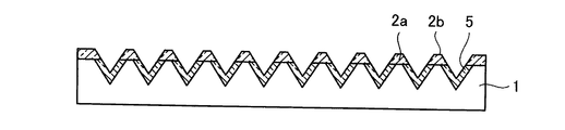
エッチングにおいては、エッチング液の濃度、エッチング液の温度、エッチング時間等のエッチング条件を制御することにより、ランダムピラミッドの頂点部分に未エッチング領域2bを残す様にエッチングの進行状態を制御する。このようなエッチングにより、凹部が基板1の内部に達するとともに、ランダムピラミッドの頂点部分にのみ未エッチング領域2bが残存した粗面形状4が形成される。そして、エッチングされずに残った微細な第1の拡散層2aは、未エッチング領域2bの下部周辺にのみ残存し、基板1の受光側の全面に分散配置される。
In the etching, by controlling the etching conditions such as the concentration of the etching solution, the temperature of the etching solution, and the etching time, the etching progress state is controlled so that the
第5の工程では、たとえばフッ酸により保護膜3aを除去し、粗面形状4を露出させる(図1−5)。
In the fifth step, the
第6の工程では、基板1の受光面側(第1の拡散層2a側)にn型不純物拡散層である第2の不純物拡散層5(以下、第2の拡散層5と呼ぶ)を形成する(図1−6)。すなわち、基板1を熱拡散路に投入し、オキシ塩化リン(POCl3)を用いたリン(P)の熱拡散により、たとえばシート抵抗が80Ω/□〜120Ω/□の第2の拡散層5を形成する。リン(P)の熱拡散は、第1の濃度よりも低い第2の濃度で行われる。したがって、第2の拡散層5は、第1の濃度よりも低い第2の濃度でリン(P)が拡散された低濃度拡散層(高抵抗領域)である。
In the sixth step, the second impurity diffusion layer 5 (hereinafter referred to as the second diffusion layer 5), which is an n-type impurity diffusion layer, is formed on the light receiving surface side (
ここで、第2の濃度は、第1の濃度よりも低い。このため、低濃度拡散層である第2の拡散層5は粗面形状4の斜面にのみが形成され、ランダムピラミッドの頭頂部に残存している第1の拡散層2aはそのまま高濃度拡散層とされる。そして、高濃度拡散層(低抵抗領域)である微細な第1の拡散層2aは、基板1の受光側の全面に分散配置されている。
Here, the second concentration is lower than the first concentration. For this reason, the
第7の工程では、粗面形状4が形成された基板1の受光面側(第1の拡散層2a側)にたとえばプラズマCVD法によりシリコン窒化膜からなる反射防止膜6を形成する(図1−7)。シリコン窒化膜の形成は、プラズマCVD法の代わりにスパッタリング法など他の手法により行っても構わない。
In the seventh step, an
第8の工程では、基板1に電極となる金属ペーストをスクリーン印刷により塗布する(図1−8)。基板1の表側(受光面側)では、たとえば銀の混入した銀ペースト7aを線幅100μmのグリッド電極形状およびバス電極形状に櫛形に塗布する。基板1の裏面側では、アルミニウムの混入したアルミニウムペースト8aをスクリーン印刷により全面に塗布する。なお、図1−8においては、グリッド電極形状に塗布した銀ペースト7aおよびアルミニウムペースト8aのみを示している。
In the eighth step, a metal paste to be an electrode is applied to the
第9の工程では、金属ペーストの焼成処理を実施して受光面側電極7と裏面電極8とを形成する(図1−9)。焼成は、大気雰囲気中においてたとえば800℃〜900℃で実施する。焼成により銀ペースト7aは固化するとともに反射防止膜6を侵食し、第1の拡散層2aおよび第2の拡散層5と電気的な接続が形成される。このとき、粗面形状4の部分に電極が形成されることで、第1の拡散層2aおよび第2の拡散層5と受光面側電極7との接触面積が増えて接続抵抗が低減されるとともに機械的な接続強度も増す。その後、基板1の外周部のpn接合のショート部分をレーザカットで除去する。以上のようにして、本実施の形態にかかる光起電力装置であって、選択エミッタ構造に類似の拡散層構造を有する光起電力装置が作製される。
In the ninth step, the metal paste is fired to form the light-receiving
比較のため、レジストパターンを用いる選択エミッタ型光起電力装置の製造方法を図2−1〜図2−6に示す。なお、図1−1〜図1−9と同じ部材については同じ符号を付す。まず、第11の工程では、基板1の一面側の表面に不純物を拡散して高濃度拡散層(低抵抗領域)である第1の拡散層2aを形成する(図2−1)。
For comparison, a manufacturing method of a selective emitter type photovoltaic device using a resist pattern is shown in FIGS. In addition, the same code | symbol is attached | subjected about the same member as FIGS. 1-1 to FIGS. 1-9. First, in the eleventh step, the
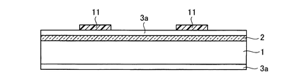
第12の工程では、第1の拡散層2aの表面に保護膜3aを被着し、さらにその上に受光面側電極の形成領域にレジストパターン11を形成する(図2−2)。
In the twelfth step, a
第13の工程では、レジストパターン11をマスクとして基板1の受光面側(第1の拡散層2a側)に形成された保護膜3aにブラスト加工処理を施して、保護膜3aに開口3bを形成する(図2−3)。ここで、保護膜3aにおけるレジストパターン11で覆われている部分には開口3bは形成されず、開口未形成部3cとされる。
In the thirteenth step, the
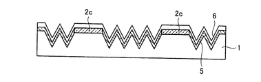
第14の工程では、レジストパターン11を除去した後、開口3bが形成された保護膜3aおよび開口未形成部3cをマスクとして、基板1の受光面側(第1の拡散層2a側)の一面に対して異方性エッチングとしてアルカリ水溶液を用いたウエットエッチングを施して、基板1の受光面側(第1の拡散層2a側)の粗面化を行う(図2−4)。このエッチングにより、開口未形成部3cの下部領域以外では、第1の拡散層2aは除去される。そして、基板1の表面における開口未形成部3cの下部領域には、受光面側電極の形成領域となる平坦な表面を有する第1の不純物拡散層2c(以下、第1の拡散層2cと呼ぶ)が残存する。また、基板1の表面におけるこれ以外の領域には、ランダムピラミッドと呼ばれる凹凸形状からなる粗面形状4が形成される。
In the fourteenth step, after removing the resist
第15の工程では、たとえばフッ酸により保護膜3aおよび開口未形成部3cを除去する(図2−5)。
In the fifteenth step, the
第16の工程では、基板1の受光面側に低濃度拡散層(高抵抗領域)である第2の拡散層5を形成する(図2−6)。第1の拡散層2cは既に高濃度拡散層とされているため、低濃度拡散層である第2の拡散層5は粗面形状4の斜面にのみ形成され、第1の拡散層2cはそのまま高濃度拡散層とされる。
In the sixteenth step, the
第17の工程では、粗面形状4が形成された基板1の受光面側にたとえばプラズマCVD法によりシリコン窒化膜からなる反射防止膜6を形成する(図2−7)。
In the seventeenth step, an
第18の工程では、基板1に電極となる金属ペーストをスクリーン印刷により塗布する(図2−8)。基板1の表側(受光面側)では、たとえば銀の混入した銀ペースト7aを線幅100μmのグリッド電極形状およびバス電極形状に櫛形に塗布する。基板1の裏面側では、アルミニウムの混入したアルミニウムペースト8aをスクリーン印刷により全面に塗布する。なお、図2−8においては、グリッド電極形状に塗布した銀(Ag)ペースト7aおよびアルミニウムペースト8aのみを示している。ここで、銀ペースト7aは、高濃度拡散層である第1の拡散層2cに合わせて印刷する必要がある。
In the 18th step, a metal paste to be an electrode is applied to the
第19の工程では、金属ペーストの焼成処理を実施して受光面側電極7と裏面電極8とを形成する(図2−9)。その後、基板1の外周部のpn接合のショート部分をレーザカットで除去する。以上のようにして、選択エミッタ型光起電力装置が作製される。
In the nineteenth step, the metal paste is fired to form the light-receiving
上記の本実施の形態にかかる光起電力装置の製造方法とレジストパターンを用いる光起電力装置の製造方法とを比較すると、本実施の形態にかかる光起電力装置の製造方法ではレジストパターン11の形成は不要である。このため、本実施の形態にかかる光起電力装置の製造方法は、製造が簡略であり、且つ製造コストが安い。
When the method for manufacturing a photovoltaic device according to the present embodiment is compared with the method for manufacturing a photovoltaic device using a resist pattern, in the method for manufacturing a photovoltaic device according to the present embodiment, the resist
図3−1は、上述した本実施の形態にかかる光起電力装置の製造方法において、第2の拡散層5が形成された時点(第6の工程、図1−6)の基板1の受光面側の状態を模式的に示す平面図である。図3−2は、図3−1の一部を拡大して示す拡大図である。図4は、上述したレジストパターンを用いる選択エミッタ型光起電力装置の製造方法において、第2の拡散層5が形成された時点(第16の工程、図2−6)の基板1の受光面側の状態を模式的に示す平面図である。
FIG. 3-1 shows the light reception of the
図3に示すように本実施の形態にかかる光起電力装置の製造方法においては、高濃度拡散層(低抵抗領域)である微細な第1の拡散層2aが基板1の受光側の全面に微細に分散配置されている。このため、基板1の受光側のどの位置に受光面電極を形成しても、受光面電極が高濃度拡散層(低抵抗領域)である微細な第1の拡散層2a上に位置することになるため、第8の工程における金属ペーストの印刷時において印刷位置の位置合わせを厳密に行う必要がない。
As shown in FIG. 3, in the method of manufacturing the photovoltaic device according to the present embodiment, the fine
一方、図4に示すようにレジストパターンを用いる選択エミッタ型光起電力装置の製造方法においては、高濃度拡散層(低抵抗領域)である第1の拡散層2cが受光面側電極の形成領域のみに作り分けられている。このため、第18の工程における金属ペーストの印刷時において第1の拡散層2cに厳密に印刷位置を合わせる必要があり、負荷が大きい。したがって、本実施の形態にかかる光起電力装置の製造方法は、レジストパターンを用いる光起電力装置の製造方法に比べて、工程が簡略であり、負荷も少ない。
On the other hand, in the method of manufacturing a selective emitter type photovoltaic device using a resist pattern as shown in FIG. 4, the
また、レジストパターンを用いる選択エミッタ型光起電力装置の製造方法では、高濃度拡散層(低抵抗領域)である第1の拡散層2cにおいて電極幅以外の部分(受光面側電極7が形成されていない部分)は電子の再結合領域となり好ましくないが、金属ペーストの印刷の位置あわせ精度には限界がある。したがって、第1の拡散層2cに起因した特性低下は避けられない。
In the method of manufacturing a selective emitter type photovoltaic device using a resist pattern, a portion other than the electrode width (light receiving surface side electrode 7) is formed in the
これに対して、本実施の形態にかかる光起電力装置の製造方法においては、高濃度拡散層(低抵抗領域)である微細な第1の拡散層2aの総面積がレジストパターンを用いる選択エミッタ型光起電力装置の製造方法における第1の拡散層2cの面積と同等またはそれ以下であれば、基板1の受光面側において受光面側電極7が形成されていない領域の第1の拡散層2aに起因した特性低下は無視することができる。
On the other hand, in the method for manufacturing the photovoltaic device according to the present embodiment, the total area of the fine
また、本実施の形態にかかる光起電力装置においては、第1の拡散層2aは高濃度拡散層(低抵抗領域)であり、また第1の工程と第6の工程とにおいてリン(P)の拡散が2回行われるため、その他の領域に対してシート抵抗が低い状態となる。そして、第1の拡散層2aが基板1の受光側の全面に点在することによって、その上に形成された受光面側電極7との接続抵抗を低減し、光照射により生成した電子の収集効率を向上させて光電変換効率を向上させることができる。
In the photovoltaic device according to the present embodiment, the
なお、この第1の拡散層2aは受光面側電極の下部領域以外では電子の再結合領域となる。このため、基板1の受光面側の面積に対する第1の拡散層2a(未エッチング領域2b)の面積の面積比として光電変換効率が最大となる最適値が存在し、検討の結果、3%〜15%が最適であることを見出した。ただし、この値は高濃度拡散層(低抵抗領域)である第1の拡散層2aとその他の領域とのシート抵抗の大小関係(比)でも異なり、シート抵抗の比が大きい場合は少なめ、シート抵抗の比が小さい場合は大きめが最適値となる。
The
上述したように、本実施の形態によれば、レジストパターンを用いる選択エミッタ型光起電力装置の製造方法よりも簡略な工程により、受光面を高抵抗化しつつ受光面側電極7の基板1との接続抵抗を低減可能な選択エミッタ構造に類似の拡散層構造を有し、選択エミッタ構造と同等以上の高い光電変換効率を有する光起電力装置が得られる。そして、本実施の形態によれば、光起電力装置の製造コストの低減および発電コストの低減が可能である。
As described above, according to the present embodiment, the
つぎに、具体的な実施例に基づいて本発明を説明する。上述した本実施の形態にかかる光起電力装置の製造方法により実施例1および実施例2の光起電力装置を作製した。実施例1の光起電力装置は、第1の拡散層2aのシート抵抗を20Ω/□、基板1の受光面側におけるその他の領域(第2の拡散層5)のシート抵抗を120Ω/□として作製した。実施例2の光起電力装置は、第1の拡散層2aのシート抵抗を50Ω/□、基板1の受光面側におけるその他の領域(第2の拡散層5)のシート抵抗を80Ω/□として作製した。
Next, the present invention will be described based on specific examples. The photovoltaic devices of Example 1 and Example 2 were manufactured by the method for manufacturing a photovoltaic device according to this embodiment described above. In the photovoltaic device of Example 1, the sheet resistance of the
ここで、実施例1および実施例2の光起電力装置については、それぞれ基板1の受光面側の面積に対する第1の拡散層2aの面積の面積比を変えて複数作製し、光電変換効率が最大となる面積比の最適値を検討した。その結果、実施例1の光起電力装置においては、最適な面積比は3%〜9%程度であった。また、実施例2の光起電力装置においては、最適な面積比は10%〜15%程度であった。
Here, a plurality of photovoltaic devices of Example 1 and Example 2 were produced by changing the area ratio of the area of the
また、比較のため、上述したレジストパターンを用いる選択エミッタ型光起電力装置の製造方法により比較例の選択エミッタ型光起電力装置を作製した。比較例の選択エミッタ型光起電力装置は、第1の拡散層2cのシート抵抗を50Ω/□、基板の受光面側におけるその他の領域(第2の拡散層5)のシート抵抗を80Ω/□として作製した。比較例の選択エミッタ型光起電力装置においては、基板の受光面側の面積に対する第1の拡散層2cの面積の面積比を14%とした。
For comparison, a selective emitter type photovoltaic device of a comparative example was manufactured by the method of manufacturing a selective emitter type photovoltaic device using the resist pattern described above. In the selective emitter type photovoltaic device of the comparative example, the sheet resistance of the
つぎに、上記の面積比を5%とした実施例1の光起電力装置、上記の面積比を12%とした実施例2の光起電力装置および比較例の選択エミッタ型光起電力装置の特性として、開放電圧Voc、短絡電流密度Jsc、曲線因子FF、光電変換効率を調べた。その結果を表1に示す。 Next, the photovoltaic device of Example 1 in which the area ratio is 5%, the photovoltaic device of Example 2 in which the area ratio is 12%, and the selective emitter type photovoltaic device of the comparative example are as follows. As characteristics, open circuit voltage Voc, short circuit current density Jsc, fill factor FF, and photoelectric conversion efficiency were examined. The results are shown in Table 1.

表1から分かるように、実施例1および、実施例2の光起電力装置においては、開放電圧Vocが比較例の光起電力装置よりも低いが、短絡電流密度Jscが増加することにより比較例よりも光電変換効率が向上していることがわかる。したがって、実施例1および実施例2の光起電力装置の方が比較例の選択エミッタ型光起電力装置よりも製造工程が簡略でありながら、良好な光起電力特性が得られると言える。 As can be seen from Table 1, in the photovoltaic devices of Example 1 and Example 2, the open-circuit voltage Voc is lower than that of the photovoltaic device of the comparative example, but the short-circuit current density Jsc is increased to increase the comparative example. It can be seen that the photoelectric conversion efficiency is improved. Therefore, it can be said that the photovoltaic devices of Example 1 and Example 2 can obtain better photovoltaic characteristics while the manufacturing process is simpler than that of the selective emitter type photovoltaic device of the comparative example.
また、上記の実施の形態で説明した構成を有する光起電力装置を複数形成し、隣接する光起電力装置同士を電気的に直列または並列に接続することにより、光電変換効率に優れた太陽電池モジュールを安価に実現できる。この場合は、たとえば隣接する光起電力装置の一方の受光面側電極7と他方の裏面電極8とを電気的に接続すればよい。
In addition, a plurality of photovoltaic devices having the configuration described in the above embodiment are formed, and adjacent photovoltaic devices are electrically connected in series or in parallel, so that a solar cell with excellent photoelectric conversion efficiency is obtained. Modules can be realized at low cost. In this case, for example, one light receiving
以上のように、本発明にかかる光起電力装置は、選択エミッタ構造に類似の拡散層構造を有し、光電変換効率に優れた光起電力装置の実現に有用である。 As described above, the photovoltaic device according to the present invention has a diffusion layer structure similar to the selective emitter structure, and is useful for realizing a photovoltaic device having excellent photoelectric conversion efficiency.
1 単結晶シリコン基板(基板)
2a 第1の不純物拡散層(第1の拡散層)
2b 未エッチング領域
2c 第1の不純物拡散層(第1の拡散層)
3a 保護膜
3b 開口
3c 開口未形成部
4 粗面形状
5 第2の不純物拡散層(第2の拡散層)
6 反射防止膜
7a 銀ペースト
7 受光面側電極
8 裏面電極
8a アルミニウムペースト
11 レジストパターン
1 Single crystal silicon substrate (substrate)
2a First impurity diffusion layer (first diffusion layer)
6
Claims (8)
前記単結晶シリコン基板の一面側の全面において前記凹凸形状の凸部の頂部に分散配置され、第2導電型の不純物元素が第1の濃度で拡散した複数の第1の拡散層と、
前記単結晶シリコン基板の一面側において前記第1の拡散層以外の領域に形成され、前記第2導電型の不純物元素が前記第1の濃度よりも低い第2の濃度で拡散した第2の拡散層と、
前記第1の拡散層に電気的に接続して前記単結晶シリコン基板の一面側に形成された受光面側電極と、
前記単結晶シリコン基板の他面側に形成された裏面側電極と、
を備えることを特徴とする光起電力装置。 A first-conductivity-type single crystal silicon substrate having a concavo-convex shape formed on one surface side;
A plurality of first diffusion layers that are dispersed and arranged on top of the convex portions of the concavo-convex shape over the entire surface on one surface side of the single crystal silicon substrate, and in which the impurity element of the second conductivity type diffuses at a first concentration;
A second diffusion formed in a region other than the first diffusion layer on one surface side of the single crystal silicon substrate, wherein the impurity element of the second conductivity type is diffused at a second concentration lower than the first concentration. Layers,
A light receiving surface side electrode electrically connected to the first diffusion layer and formed on one surface side of the single crystal silicon substrate;
A back side electrode formed on the other side of the single crystal silicon substrate;
A photovoltaic device comprising:
前記第2の拡散層のシート抵抗が80Ω/□〜120Ω/□であり、
前記第1の拡散層の合計の面積が前記単結晶シリコン基板の一面側の面積に対して3%〜15%であること、
を特徴とする請求項1に記載の光起電力装置。 The sheet resistance of the first diffusion layer is 20Ω / □ to 50Ω / □,
The sheet resistance of the second diffusion layer is 80Ω / □ to 120Ω / □,
The total area of the first diffusion layer is 3% to 15% with respect to the area of one surface side of the single crystal silicon substrate;
The photovoltaic device according to claim 1.
前記第1の拡散層の表面に保護膜を被着する第2の工程と、
前記保護膜にブラスト加工処理を施して前記保護膜の全面に複数の開口を形成する第3の工程と、
前記開口が形成された前記保護膜をエッチングマスクとして前記保護膜が耐性を有する条件で前記単結晶シリコン基板の一面側に対して異方性エッチングを施すことにより、前記単結晶シリコン基板の一面側に凹凸形状を形成するとともに前記保護膜の下部領域に前記異方性エッチングが施されていない前記第1の拡散層を残存させて前記第1の拡散層を前記単結晶シリコン基板の一面側の全面に分散配置する第4の工程と、
前記保護膜を除去する第5の工程と、
前記単結晶シリコン基板の一面側に第2導電型の不純物元素を前記第1の濃度よりも低い第2の濃度で拡散させて、前記単結晶シリコン基板の一面側における前記第1の拡散層以外の領域に第2の拡散層を形成する第6の工程と、
前記単結晶シリコン基板の一面側に電極を形成する第7の工程と、
前記単結晶シリコン基板の他面側に電極を形成する第8の工程と、
を含むことを特徴とする光起電力装置の製造方法。 A first step of diffusing a second conductivity type impurity element at a first concentration to form a first diffusion layer on the entire surface of one surface side of the first conductivity type single crystal silicon substrate;
A second step of depositing a protective film on the surface of the first diffusion layer;
A third step of subjecting the protective film to blasting to form a plurality of openings on the entire surface of the protective film;
One surface side of the single crystal silicon substrate is subjected to anisotropic etching with respect to the one surface side of the single crystal silicon substrate under the condition that the protective film is resistant with the protective film having the opening formed as an etching mask. The first diffusion layer is formed on the one surface side of the single crystal silicon substrate by forming the concavo-convex shape and leaving the first diffusion layer not subjected to the anisotropic etching in the lower region of the protective film. A fourth step of dispersively arranging the entire surface;
A fifth step of removing the protective film;
An impurity element of a second conductivity type is diffused at one surface side of the single crystal silicon substrate at a second concentration lower than the first concentration, so that other than the first diffusion layer on the one surface side of the single crystal silicon substrate. A sixth step of forming a second diffusion layer in the region;
A seventh step of forming an electrode on one side of the single crystal silicon substrate;
An eighth step of forming electrodes on the other surface side of the single crystal silicon substrate;
A method for manufacturing a photovoltaic device, comprising:
を特徴とする請求項3に記載の光起電力装置の製造方法。 In the fourth step, adjusting the etching conditions so that an unetched region not subjected to the anisotropic etching remains in the first diffusion layer in the lower region of the protective film;
The method for manufacturing a photovoltaic device according to claim 3.
を特徴とする請求項3または4に記載の光起電力装置の製造方法。 In the fourth step, wet etching is performed using at least one of an alkaline aqueous solution and an alkaline aqueous solution containing an additive as an etching solution;
The method for manufacturing a photovoltaic device according to claim 3 or 4, wherein:
を特徴とする請求項3〜5のいずれか1つに記載の光起電力装置の製造方法。 The sheet resistance of the first diffusion layer is 20Ω / □ to 50Ω / □, the sheet resistance of the second diffusion layer is 80Ω / □ to 120Ω / □, and the area of the unetched region is the single crystal silicon substrate 3% to 15% with respect to the area on the one surface side,
The method for manufacturing a photovoltaic device according to any one of claims 3 to 5, wherein:
を特徴とする請求項3〜6のいずれか1つに記載の光起電力装置の製造方法。 The protective film is any one of a silicon thermal oxide film, a silicon oxide film or a silicon nitride film formed by chemical deposition or physical deposition, or a combination thereof;
A method for manufacturing a photovoltaic device according to any one of claims 3 to 6.
を特徴とする光起電力モジュール。 At least two or more of the photovoltaic devices according to claim 1 or 2 are electrically connected in series or in parallel;
A photovoltaic module characterized by.
Priority Applications (1)
| Application Number | Priority Date | Filing Date | Title |
|---|---|---|---|
| JP2011068592A JP5496136B2 (en) | 2011-03-25 | 2011-03-25 | Photovoltaic device and photovoltaic module |
Applications Claiming Priority (1)
| Application Number | Priority Date | Filing Date | Title |
|---|---|---|---|
| JP2011068592A JP5496136B2 (en) | 2011-03-25 | 2011-03-25 | Photovoltaic device and photovoltaic module |
Publications (2)
| Publication Number | Publication Date |
|---|---|
| JP2012204660A true JP2012204660A (en) | 2012-10-22 |
| JP5496136B2 JP5496136B2 (en) | 2014-05-21 |
Family
ID=47185286
Family Applications (1)
| Application Number | Title | Priority Date | Filing Date |
|---|---|---|---|
| JP2011068592A Expired - Fee Related JP5496136B2 (en) | 2011-03-25 | 2011-03-25 | Photovoltaic device and photovoltaic module |
Country Status (1)
| Country | Link |
|---|---|
| JP (1) | JP5496136B2 (en) |
Cited By (8)
| Publication number | Priority date | Publication date | Assignee | Title |
|---|---|---|---|---|
| WO2014158586A1 (en) * | 2013-03-13 | 2014-10-02 | Gtat Corporation | Free-standing metallic article with overplating |
| WO2014159146A1 (en) * | 2013-03-13 | 2014-10-02 | Gtat Corporation | Free-standing metallic article for semiconductors |
| US8936709B2 (en) | 2013-03-13 | 2015-01-20 | Gtat Corporation | Adaptable free-standing metallic article for semiconductors |
| TWI643355B (en) * | 2013-03-13 | 2018-12-01 | 美商梅林太陽能科技股份有限公司 | Free-standing metallic article for semiconductors |
| CN109509800A (en) * | 2018-12-26 | 2019-03-22 | 浙江晶科能源有限公司 | A kind of imbrication photovoltaic module and photovoltaic generating system |
| CN113571610A (en) * | 2021-07-23 | 2021-10-29 | 广东中图半导体科技股份有限公司 | Substrate surface micro-processing method, composite substrate and LED epitaxial wafer |
| KR20220078466A (en) * | 2020-12-03 | 2022-06-10 | 호서대학교 산학협력단 | PN junction solar cell having silica pyramid structure and manufacturing method thereof |
| CN115911147A (en) * | 2022-11-16 | 2023-04-04 | 宁夏隆基乐叶科技有限公司 | Selective emitter, preparation method thereof, solar cell and solar module |
Citations (9)
| Publication number | Priority date | Publication date | Assignee | Title |
|---|---|---|---|---|
| JPH0661515A (en) * | 1991-12-27 | 1994-03-04 | Rudolf Hezel | Solar cell and its manufacture |
| JPH11508088A (en) * | 1995-06-21 | 1999-07-13 | フラウンホファー.ゲゼルシャフト.ツール.フォルデンウング.デール.アンゲヴァンドテン.フォルシュング.エー.ファウ | Solar cell having surface textured radiating layer |
| JP2003158274A (en) * | 2001-11-20 | 2003-05-30 | Sharp Corp | Method for manufacturing planar solar battery cell |
| JP2006073832A (en) * | 2004-09-02 | 2006-03-16 | Sharp Corp | Solar battery and method of manufacturing the same |
| WO2009118861A1 (en) * | 2008-03-27 | 2009-10-01 | 三菱電機株式会社 | Photovolatic power device and method for manufacturing the same |
| WO2009128324A1 (en) * | 2008-04-17 | 2009-10-22 | 三菱電機株式会社 | Method for roughening substrate surface and method for manufacturing photovoltaic device |
| JP2010130023A (en) * | 2008-11-26 | 2010-06-10 | Samsung Electronics Co Ltd | Solar cell and method of manufacturing the same |
| WO2010109692A1 (en) * | 2009-03-25 | 2010-09-30 | 三菱電機株式会社 | Method for roughening substrate surface and method for manufacturing photovoltaic device |
| JP2011524638A (en) * | 2008-06-11 | 2011-09-01 | インテバック・インコーポレイテッド | Semiconductor device and solar cell manufacturing method |
-
2011
- 2011-03-25 JP JP2011068592A patent/JP5496136B2/en not_active Expired - Fee Related
Patent Citations (9)
| Publication number | Priority date | Publication date | Assignee | Title |
|---|---|---|---|---|
| JPH0661515A (en) * | 1991-12-27 | 1994-03-04 | Rudolf Hezel | Solar cell and its manufacture |
| JPH11508088A (en) * | 1995-06-21 | 1999-07-13 | フラウンホファー.ゲゼルシャフト.ツール.フォルデンウング.デール.アンゲヴァンドテン.フォルシュング.エー.ファウ | Solar cell having surface textured radiating layer |
| JP2003158274A (en) * | 2001-11-20 | 2003-05-30 | Sharp Corp | Method for manufacturing planar solar battery cell |
| JP2006073832A (en) * | 2004-09-02 | 2006-03-16 | Sharp Corp | Solar battery and method of manufacturing the same |
| WO2009118861A1 (en) * | 2008-03-27 | 2009-10-01 | 三菱電機株式会社 | Photovolatic power device and method for manufacturing the same |
| WO2009128324A1 (en) * | 2008-04-17 | 2009-10-22 | 三菱電機株式会社 | Method for roughening substrate surface and method for manufacturing photovoltaic device |
| JP2011524638A (en) * | 2008-06-11 | 2011-09-01 | インテバック・インコーポレイテッド | Semiconductor device and solar cell manufacturing method |
| JP2010130023A (en) * | 2008-11-26 | 2010-06-10 | Samsung Electronics Co Ltd | Solar cell and method of manufacturing the same |
| WO2010109692A1 (en) * | 2009-03-25 | 2010-09-30 | 三菱電機株式会社 | Method for roughening substrate surface and method for manufacturing photovoltaic device |
Cited By (12)
| Publication number | Priority date | Publication date | Assignee | Title |
|---|---|---|---|---|
| WO2014158586A1 (en) * | 2013-03-13 | 2014-10-02 | Gtat Corporation | Free-standing metallic article with overplating |
| WO2014159146A1 (en) * | 2013-03-13 | 2014-10-02 | Gtat Corporation | Free-standing metallic article for semiconductors |
| US8916038B2 (en) | 2013-03-13 | 2014-12-23 | Gtat Corporation | Free-standing metallic article for semiconductors |
| US8936709B2 (en) | 2013-03-13 | 2015-01-20 | Gtat Corporation | Adaptable free-standing metallic article for semiconductors |
| US8940998B2 (en) | 2013-03-13 | 2015-01-27 | Gtat Corporation | Free-standing metallic article for semiconductors |
| CN105009302A (en) * | 2013-03-13 | 2015-10-28 | Gtat公司 | Free-standing metallic article with overplating |
| TWI643355B (en) * | 2013-03-13 | 2018-12-01 | 美商梅林太陽能科技股份有限公司 | Free-standing metallic article for semiconductors |
| CN109509800A (en) * | 2018-12-26 | 2019-03-22 | 浙江晶科能源有限公司 | A kind of imbrication photovoltaic module and photovoltaic generating system |
| KR20220078466A (en) * | 2020-12-03 | 2022-06-10 | 호서대학교 산학협력단 | PN junction solar cell having silica pyramid structure and manufacturing method thereof |
| KR102600281B1 (en) | 2020-12-03 | 2023-11-09 | 호서대학교 산학협력단 | PN junction solar cell having silica pyramid structure and manufacturing method thereof |
| CN113571610A (en) * | 2021-07-23 | 2021-10-29 | 广东中图半导体科技股份有限公司 | Substrate surface micro-processing method, composite substrate and LED epitaxial wafer |
| CN115911147A (en) * | 2022-11-16 | 2023-04-04 | 宁夏隆基乐叶科技有限公司 | Selective emitter, preparation method thereof, solar cell and solar module |
Also Published As
| Publication number | Publication date |
|---|---|
| JP5496136B2 (en) | 2014-05-21 |
Similar Documents
| Publication | Publication Date | Title |
|---|---|---|
| JP5496136B2 (en) | Photovoltaic device and photovoltaic module | |
| US8697475B2 (en) | Solar cell and method for manufacturing the same | |
| JP4980494B2 (en) | Solar cell and manufacturing method thereof | |
| JP5220197B2 (en) | Solar cell and manufacturing method thereof | |
| JP2009135338A (en) | Solar cell, and manufacturing method of solar cell | |
| US20160197207A1 (en) | Solar cell, solar cell module, and manufacturing method of solar cell | |
| WO2009081684A1 (en) | Photoelectric conversion device and method for manufacturing photoelectric conversion device | |
| JP5460860B2 (en) | Solar cell element and manufacturing method thereof | |
| JP5777798B2 (en) | Method for manufacturing solar battery cell | |
| JP2016122749A (en) | Solar battery element and solar battery module | |
| US9997647B2 (en) | Solar cells and manufacturing method thereof | |
| JP4937233B2 (en) | Method for roughening substrate for solar cell and method for manufacturing solar cell | |
| KR101659451B1 (en) | Solar cell and manufacturing method thereof | |
| JP2013048126A (en) | Photovoltaic device and manufacturing method thereof | |
| JPWO2012104997A1 (en) | SOLAR CELL, ITS MANUFACTURING METHOD, AND SOLAR CELL MODULE | |
| TWI761662B (en) | Manufacturing method of solar cell | |
| JP2001257371A (en) | Method for manufacturing solar cell, solar cell and condensing type solar cell module | |
| JP5349523B2 (en) | Manufacturing method of solar cell | |
| JP5665975B2 (en) | SOLAR CELL, ITS MANUFACTURING METHOD, SOLAR CELL MODULE | |
| JP5029921B2 (en) | Method for manufacturing solar battery cell | |
| JP6125042B2 (en) | Method for manufacturing solar battery cell | |
| JP2011018748A (en) | Method of manufacturing solar battery cell | |
| WO2014118923A1 (en) | Photovoltaic device, method for fabricating same, and photovoltaic module | |
| JP6663492B2 (en) | Solar cell, method for manufacturing solar cell, and system for manufacturing solar cell | |
| WO2020022044A1 (en) | Manufacturing method for solar cell |
Legal Events
| Date | Code | Title | Description |
|---|---|---|---|
| A621 | Written request for application examination |
Free format text: JAPANESE INTERMEDIATE CODE: A621 Effective date: 20120927 |
|
| A131 | Notification of reasons for refusal |
Free format text: JAPANESE INTERMEDIATE CODE: A131 Effective date: 20130723 |
|
| A977 | Report on retrieval |
Free format text: JAPANESE INTERMEDIATE CODE: A971007 Effective date: 20130724 |
|
| A521 | Request for written amendment filed |
Free format text: JAPANESE INTERMEDIATE CODE: A523 Effective date: 20130920 |
|
| TRDD | Decision of grant or rejection written | ||
| A01 | Written decision to grant a patent or to grant a registration (utility model) |
Free format text: JAPANESE INTERMEDIATE CODE: A01 Effective date: 20140204 |
|
| A61 | First payment of annual fees (during grant procedure) |
Free format text: JAPANESE INTERMEDIATE CODE: A61 Effective date: 20140304 |
|
| R150 | Certificate of patent or registration of utility model |
Ref document number: 5496136 Country of ref document: JP Free format text: JAPANESE INTERMEDIATE CODE: R150 |
|
| R250 | Receipt of annual fees |
Free format text: JAPANESE INTERMEDIATE CODE: R250 |
|
| LAPS | Cancellation because of no payment of annual fees |