JP2012201889A - Electroplating apparatus - Google Patents
Electroplating apparatus Download PDFInfo
- Publication number
- JP2012201889A JP2012201889A JP2011064414A JP2011064414A JP2012201889A JP 2012201889 A JP2012201889 A JP 2012201889A JP 2011064414 A JP2011064414 A JP 2011064414A JP 2011064414 A JP2011064414 A JP 2011064414A JP 2012201889 A JP2012201889 A JP 2012201889A
- Authority
- JP
- Japan
- Prior art keywords
- electrodes
- metal
- electrode
- length
- passing direction
- Prior art date
- Legal status (The legal status is an assumption and is not a legal conclusion. Google has not performed a legal analysis and makes no representation as to the accuracy of the status listed.)
- Granted
Links
Images

Abstract
Description
本発明は、鋼帯などの金属帯の表面に電気めっき処理を施す際に適用される電気めっき装置に関するものである。 The present invention relates to an electroplating apparatus applied when performing electroplating on the surface of a metal strip such as a steel strip.
鋼板等の表面処理は、防錆や防食、装飾といった多様な目的でおこなわれるものであり、表面処理によって鋼板の品質を向上させ、その用途の多様化や広範化を図ることができる。 Surface treatment of a steel plate or the like is performed for various purposes such as rust prevention, corrosion prevention, and decoration, and the quality of the steel plate can be improved by the surface treatment, and the use can be diversified and broadened.
鋼板等の表面処理法は多岐に亘るが、その一つの処理法として、電解槽を用いた連続表面処理法があり、この方法によって製造された電気めっき鋼板などがたとえば車両の車体部材等に適用されている。なお、めっきで使用される金属も多岐に亘るが、Zn,Ni、Sn,Cr、Cuなどを単独で、もしくは、Zn−Fe合金、Zn−Ni合金、Zn−Ni−Co合金などの合金からなるめっき材料が鋼板等の表面に電気めっき処理される。 There are a wide variety of surface treatment methods for steel plates, etc., but one of the treatment methods is a continuous surface treatment method using an electrolytic cell. Electroplated steel plates produced by this method can be applied to, for example, vehicle body members. Has been. In addition, although the metal used by plating is also various, Zn, Ni, Sn, Cr, Cu, etc. are used alone or from alloys such as Zn-Fe alloy, Zn-Ni alloy, Zn-Ni-Co alloy. The plating material to be electroplated on the surface of a steel plate or the like.
この連続電気めっきの際に適用される電解槽の型式には、横型電解槽や竪型電解槽、湾曲型電解槽がある。たとえば、横型電解槽では、めっき液が水平方向に噴流する電解槽内に配設された不溶性の電極間を被めっき対象の金属帯が通板されるようになっていて、金属帯を陰極とし、陽極である電極間に金属帯を通板させる過程で金属帯の表面に電気めっきを施すものである。 The electrolytic cell types applied during the continuous electroplating include a horizontal electrolytic cell, a vertical electrolytic cell, and a curved electrolytic cell. For example, in a horizontal electrolytic cell, a metal band to be plated is passed between insoluble electrodes disposed in an electrolytic cell in which a plating solution is jetted in the horizontal direction, and the metal band is used as a cathode. Electroplating is performed on the surface of the metal strip in the process of passing the metal strip between the electrodes that are anodes.
たとえば、上記する横型電解槽においては、電解槽内でのめっき液の噴流形態が複数存在しており、電極間を通板する金属帯の通板方向と反対側の方向でめっき液を噴流させる水平タイプ片側流入式の電解槽や、電極中央から通板方向とこれと反対側の方向の2方向にめっき液を噴流させる水平タイプ中央流入式の電解槽などがある。なお、竪型電解槽においても、垂直タイプ片側流入式等の電解槽が存在する。 For example, in the horizontal electrolytic cell described above, there are a plurality of jet forms of the plating solution in the electrolytic cell, and the plating solution is jetted in the direction opposite to the plate passing direction of the metal strip passing between the electrodes. There are horizontal type one-side inflow type electrolytic cells and horizontal type central inflow type electrolytic cells in which a plating solution is jetted from the electrode center in two directions, ie, a plate passing direction and the opposite direction. Note that vertical type one-side inflow type electrolytic cells also exist in vertical type electrolytic cells.
ところで、連続電気めっき用の電解槽において一般に適用されている電極は、金属帯と一定の間隔が保持される平面状をなしている。 By the way, the electrode generally applied in the electrolytic cell for continuous electroplating has a planar shape in which a certain distance from the metal strip is maintained.
上記する平面状の電極間では一定電流密度でめっき液が電解されるが、たとえば金属帯の通板速度が比較的遅い場合に、析出するめっき金属の結晶が節状や樹枝状の結晶となり易く、このように節状や樹枝状の金属結晶が金属帯の表面にめっき処理されると、後工程で金属帯を曲げ加工等した際に、節状や樹枝状の金属結晶の界面に沿ってクラックが生じ易く、めっき品質の低下を招くといった課題が本発明者等によって特定されている。 Although the plating solution is electrolyzed at a constant current density between the above planar electrodes, for example, when the speed of passing the metal strip is relatively slow, the deposited plating metal crystals tend to be nodal or dendritic crystals. In this way, when the metal band-like or dendritic metal crystal is plated on the surface of the metal band, when the metal band is bent in a later process, along the interface of the node-like or dendritic metal crystal The present inventors have identified a problem that cracks are likely to occur and the plating quality is degraded.
ここで、従来の公開技術に目を転じるに、特許文献1には、電極の寿命を大幅に延長することを目的として、表面に凹凸部を有する電極と、この電極を用いた金属帯の連続電気めっき方法が開示されている。 Here, turning to the conventional published technique, Patent Document 1 describes that an electrode having a concavo-convex portion on the surface and a continuous metal band using this electrode are provided for the purpose of significantly extending the life of the electrode. An electroplating method is disclosed.
より具体的には、電極基体である金属基体の放電側の表面に機械加工などによって溝を設けて凹凸状とし、電極表面の実表面積を増加させた後に皮膜をコーテイングしたものである。金属基体である平板に皮膜を被覆した従来構造の電極と異なり、電極使用時の電極単位表面積当たりの電流負荷を減少させることができ、皮膜の消耗速度を小さくすることによって同一電極を長時間使用可能にする、というものである。 More specifically, a groove is provided on the discharge-side surface of the metal substrate, which is an electrode substrate, to form irregularities, and the coating is coated after increasing the actual surface area of the electrode surface. Unlike electrodes with a conventional structure where a metal plate is coated with a coating, the current load per electrode unit surface area when using the electrode can be reduced, and the same electrode can be used for a long time by reducing the consumption rate of the coating. It makes it possible.
特許文献1には上記する本発明者等によって特定されている課題の開示は一切ないものの、本発明者等によれば、電極表面を特許文献1で開示されるように凹凸状にすることで対向する電極間の距離を交互に変化させることができ(対向する凸部間で電極間距離が短くなり、対向する凹部間で電極間距離が長くなる)、たとえば設備費が高価なものとなるパルス電流を通電することなく、直流電流を通電して一つの電極間で電解電流密度を変化させることができる。 Although Patent Document 1 does not disclose any of the problems specified by the present inventors as described above, according to the present inventors, the surface of the electrode is made uneven as disclosed in Patent Document 1. The distance between the electrodes facing each other can be changed alternately (the distance between the electrodes between the convex portions facing each other is shortened, and the distance between the electrodes between the concave portions facing each other is increased). For example, the equipment cost is expensive. It is possible to change the electrolytic current density between one electrode by applying a direct current without applying a pulse current.
このように一つの電極間で電解電流密度を変化させることにより、対向する凸部間には相対的に高電流密度域を形成してここで緻密な金属結晶を析出させ、対向する凹部間には相対的に低電流密度域を形成して金属結晶を析出・成長させ、これらが交互に繰り返されることで、節状や樹枝状の金属結晶が生じ難いことを本発明者等は見出している。 In this way, by changing the electrolytic current density between one electrode, a relatively high current density region is formed between the convex portions facing each other, and a dense metal crystal is deposited here, and between the concave portions facing each other. The present inventors have found that, by forming a relatively low current density region to precipitate and grow metal crystals and repeating these alternately, no node-like or dendritic metal crystals are likely to occur. .
しかしながら、単に電極表面に凹凸部を設けただけでは金属帯とめっき層(めっき被膜)の間の密着性が不十分であることもまた、本発明者等によって特定されている。 However, it has also been specified by the present inventors that the adhesiveness between the metal strip and the plating layer (plating film) is insufficient only by providing an uneven surface on the electrode surface.
本発明は上記する問題に鑑みてなされたものであり、金属帯の表面に電気めっきをおこなう装置に関し、節状や樹枝状のめっき金属結晶が金属帯の表面に生じ難く、しかも、めっき層と金属帯を高い密着性のもとで電気めっき処理することのできる電気めっき装置を提供することを目的としている。 The present invention has been made in view of the above-described problems, and relates to an apparatus for performing electroplating on the surface of a metal strip. Nodular or dendritic plated metal crystals are hardly generated on the surface of the metal strip, and the plating layer and An object of the present invention is to provide an electroplating apparatus capable of electroplating a metal strip with high adhesion.
前記目的を達成すべく、本発明による電気めっき装置は、電解槽と、電解槽内で金属帯を通板させる送り機構と、電解槽内で金属帯の通板方向もしくはこれと逆の方向にめっき液を流す流通機構と、金属帯を挟む位置に配設された一対の電極と、から構成された電気めっき装置であって、前記一対の電極はともに、対応する位置でかつ通板方向に凸部と凹部を交互に備え、双方の電極の凸部間で電極間距離が短くなり、双方の凹部間で電極間距離が長くなっており、前記電極の金属帯が該電極に入ってくる入側の端部において、複数の凹部の中でも通板方向長さの最も長い凹部が配されているものである。 In order to achieve the above object, an electroplating apparatus according to the present invention comprises an electrolytic cell, a feed mechanism for passing a metal band in the electrolytic cell, and a metal band passing direction in the electrolytic cell or in the opposite direction. An electroplating apparatus comprising a flow mechanism for flowing a plating solution and a pair of electrodes arranged at a position sandwiching a metal band, both of the pair of electrodes being at a corresponding position and in a plate passing direction. Protrusions and recesses are provided alternately, the distance between the electrodes is shortened between the projections of both electrodes, the distance between the electrodes is increased between both recesses, and the metal band of the electrode enters the electrode At the entrance end, a recess having the longest length in the plate passing direction is disposed among the plurality of recesses.
本発明の電気めっき装置は、めっき液が収容された電解槽内で陽極をなす一対の電極の間に陰極をなす鋼板等の金属帯を通板させて、金属帯の表面に電気めっきをほどこす装置である。この装置は横型電解槽や竪型電解槽、湾曲型電解槽のいずれであってもよく、たとえば横型電解槽の場合には、電極間を通板する金属帯の通板方向と反対側の方向でめっき液を噴流させる水平タイプ片側流入式の電解槽や、電極中央から通板方向とこれと反対側の方向の2方向にめっき液を噴流させる水平タイプ中央流入式の電解槽などのいずれであってもよい。 In the electroplating apparatus of the present invention, a metal strip such as a steel plate forming a cathode is passed between a pair of electrodes forming an anode in an electrolytic cell in which a plating solution is accommodated, and electroplating is performed on the surface of the metal strip. It is a rubbing device. This apparatus may be a horizontal electrolytic cell, a vertical electrolytic cell, or a curved electrolytic cell. For example, in the case of a horizontal electrolytic cell, the direction opposite to the direction of the metal strip that passes between the electrodes. Either a horizontal type one-side inflow type electrolytic cell that jets the plating solution at the center, or a horizontal type one-side inflow type electrolytic cell that jets the plating solution from the center of the electrode in two directions, the plate passing direction and the opposite direction. There may be.
また、電気めっき処理されるめっき金属も何等限定されるものでなく、たとえば、ZnやNi、Sn,Cr、Cuなどの単一の純金属のほか、Zn−Fe合金やZn−Ni合金、Zn−Ni−Co合金などの合金などであってもよい。 Also, the plating metal to be electroplated is not limited in any way. For example, in addition to a single pure metal such as Zn, Ni, Sn, Cr, Cu, Zn—Fe alloy, Zn—Ni alloy, Zn An alloy such as a Ni—Co alloy may be used.
電気めっき装置を構成する一対の電極は、凹部と凸部を交互に備えて、対応する凹部間で電極間距離が長く、対応する凸部間で電極間距離が短いものであり、さらに、電極の金属帯が該電極に入ってくる入側の端部において、複数の凹部の中でも通板方向長さの最も長い凹部が配されているものである。 The pair of electrodes constituting the electroplating apparatus is provided with alternating concave portions and convex portions, the inter-electrode distance is long between the corresponding concave portions, and the inter-electrode distance is short between the corresponding convex portions. Among the plurality of concave portions, the concave portion having the longest length in the sheet passing direction is arranged at the end of the entrance side where the metal band enters the electrode.
電極が凹凸部を交互に備えていることで、パルス電流を通電することなく、一つの電極間で電解電流密度を変化させることができ、このことによって、電極間距離の短い対向する凸部間には相対的に高電流密度域を形成してここで緻密な金属結晶を析出させ、電極間距離の長い対向する凹部間には相対的に低電流密度域を形成してゆっくりと金属結晶を析出・成長させ、これらが交互に繰り返されることで、節状や樹枝状のめっき金属結晶を抑制することができる。 Since the electrodes are provided with uneven portions alternately, it is possible to change the electrolytic current density between one electrode without passing a pulse current. In this case, a relatively high current density region is formed and a dense metal crystal is deposited here, and a relatively low current density region is formed between opposing concave portions having a long inter-electrode distance to slowly form a metal crystal. By depositing and growing and repeating these alternately, it is possible to suppress node-like or dendritic plated metal crystals.
さらに、電極の金属帯が該電極に入ってくる入側の端部に凹部を設け、この凹部の通板方向長さを他の凹部に比して最も長くしたことにより、金属帯の表面におけるめっき初期の電流密度を低くすることができ、このことによってめっき金属の析出速度を抑制することができる。たとえば、この入側端部の凹部の長さを、他の凹部の長さの2倍程度に調整することができる。ここで、流通機構によって噴流されためっき液が電極間の凹凸による攪拌効果によって渦流を生じさせるが、めっき初期のめっき金属の析出速度が抑制されるとともに金属帯表面におけるめっき液が十分に攪拌され、この攪拌されためっき液を金属帯に接触させることによって、金属帯とめっき金属が析出してなるめっき層の間の密着性を高めることができる。 Furthermore, a concave portion is provided at the end of the entrance side where the metal band of the electrode enters the electrode, and the length of the concave portion in the plate passing direction is the longest compared to other concave portions, so that The current density at the initial stage of plating can be lowered, and this can suppress the deposition rate of the plating metal. For example, the length of the recess at the entry end can be adjusted to about twice the length of the other recess. Here, the plating solution jetted by the flow mechanism causes a vortex due to the stirring effect due to the unevenness between the electrodes, but the plating metal deposition rate at the initial stage of plating is suppressed and the plating solution on the surface of the metal band is sufficiently stirred. By bringing the stirred plating solution into contact with the metal strip, the adhesion between the metal strip and the plating layer formed by depositing the plating metal can be enhanced.
めっき初期の金属帯とめっき層の間の密着性が保証されれば、金属帯が電極間を通板される過程での金属析出によって所望厚のめっき層が形成されることになるが、同一種のめっき金属同士の密着性が良好であることは言うまでもないことである。 If adhesion between the metal strip at the initial stage of plating and the plating layer is ensured, a plating layer having a desired thickness is formed by metal deposition in the process of passing the metal strip between the electrodes. Needless to say, the adhesion between one kind of plated metals is good.
ここで、電極表面の凹凸形態には以下のようなものがある。
その一つは、前記通板方向長さの最も長い凹部以外の凹部と凸部の通板方向長さがすべて一定となっている形態である。
Here, there are the following forms of unevenness on the electrode surface.
One of them is a form in which the length in the plate passing direction of the recesses and the projections other than the recess having the longest length in the plate passing direction is constant.
また、他の一つは、電極の前記入側の端部から出側の端部に向かって、凹部と凸部双方の通板方向長さが漸次短くなっている形態である。 The other is a form in which the lengths in the plate passing direction of both the concave portion and the convex portion are gradually shortened from the entrance end portion to the exit end portion of the electrode.
さらに他の一つは、電極の前記入側の端部から出側の端部に向かって、凹部の通板方向長さのみが漸次短くなっている形態である。 The other is a form in which only the length of the recess in the plate passing direction is gradually shortened from the entrance end to the exit end of the electrode.
また、電極間における金属帯の通板位置と凹部の間の長さをLとした際に、凹部に対する凸部の金属帯側への突出長さがL/6〜L/3の範囲となっているのが好ましい。 Moreover, when the length between the metal plate passing position between the electrodes and the concave portion is L, the protruding length of the convex portion with respect to the concave portion toward the metal band is in the range of L / 6 to L / 3. It is preferable.
本発明者等によれば、凹部に対する凸部の金属帯側への突出長さがL/6よりも小さいと、電極内における電流密度の変化が小さすぎてめっき液の攪拌効果や節状や樹枝状のめっき金属結晶抑制効果が少ないことが特定されている。一方、突出長さがL/3よりも大きいと、対向する凸部間の距離が小さくなり過ぎて電極同士の接触の危険性が高まることが特定されており、これらのことより、上記する上下限値が規定されたものである。 According to the present inventors, when the protruding length of the convex portion with respect to the concave portion to the metal band side is smaller than L / 6, the current density change in the electrode is too small and the plating solution stirring effect or nodal shape It has been identified that the dendritic plated metal crystal suppressive effect is small. On the other hand, when the protrusion length is larger than L / 3, it has been specified that the distance between the convex portions facing each other becomes too small and the risk of contact between the electrodes increases. The lower limit is specified.
さらに、電極間における金属帯の通板位置と凹部の間の長さをLとした際に、凹部と凸部の通板方向長さがともに、2L〜10Lの範囲となっているのが好ましい。 Furthermore, when the length between the plate passing position of the metal strip between the electrodes and the recess is L, it is preferable that both the length in the plate passing direction of the recess and the projection is in the range of 2L to 10L. .
本発明者等によれば、凹部と凸部の通板方向長さがともに2Lよりも小さいと、電流密度の変化が小さ過ぎること、凹部と凸部の通板方向長さがともに10Lよりも大きいと、噴流するめっき液が一定電流密度内に留まる時間が長くなり過ぎることより、いずれも凹凸電極による効果が少なくなることが特定されており、これらのことから上記する上下限値が規定されたものである。 According to the present inventors, if the lengths of the concave and convex portions in the plate passing direction are both less than 2L, the current density change is too small, and the concave and convex portions in the plate passing direction length are both less than 10L. If it is large, it has been specified that the effect of the concavo-convex electrode is reduced because the time for the sprayed plating solution to stay within a certain current density becomes too long. It is a thing.
以上の説明から理解できるように、本発明の電気めっき装置によれば、電気めっき装置を構成する一対の電極が凹部と凸部を交互に備え、対応する凹部間で電極間距離が長く、対応する凸部間で電極間距離が短いことにより、パルス電流を通電することなく、一つの電極間で電解電流密度を変化させることができ、このことによって、電極間距離の短い対向する凸部間には相対的に高電流密度域を形成してここで緻密な金属結晶を析出させ、電極間距離の長い対向する凹部間には相対的に低電流密度域を形成してゆっくりと金属結晶を析出・成長させ、これらが交互に繰り返されることで、節状や樹枝状のめっき金属結晶を抑制することができる。さらに、電極の金属帯が該電極に入ってくる入側の端部において、複数の凹部の中でも通板方向長さの最も長い凹部が配されていることにより、金属帯の表面におけるめっき初期の電流密度を低くすることができ、このことによってめっき金属の析出速度が抑制されるとともに金属帯表面におけるめっき液が十分に攪拌され、この攪拌されためっき液を金属帯に接触させることによって、金属帯とめっき金属が析出してなるめっき層の間の密着性を高めることができる。 As can be understood from the above description, according to the electroplating apparatus of the present invention, the pair of electrodes constituting the electroplating apparatus are provided with recesses and protrusions alternately, and the distance between the electrodes is long between the corresponding recesses. Electrode current density can be changed between one electrode without passing a pulse current due to the short inter-electrode distance between the convex portions, and thus, between the opposing convex portions having a short inter-electrode distance. In this case, a relatively high current density region is formed and a dense metal crystal is deposited here, and a relatively low current density region is formed between opposing concave portions having a long inter-electrode distance to slowly form a metal crystal. By depositing and growing and repeating these alternately, it is possible to suppress node-like or dendritic plated metal crystals. Furthermore, at the end of the entrance side where the metal band of the electrode enters the electrode, a recess having the longest length in the plate-passing direction is disposed among the plurality of recesses. The current density can be lowered, and this suppresses the deposition rate of the plating metal and sufficiently stirs the plating solution on the surface of the metal band. By bringing this stirred plating solution into contact with the metal band, the metal The adhesion between the band and the plating layer formed by depositing the plating metal can be enhanced.
以下、図面を参照して本発明の電気めっき装置の実施の形態を説明する。なお、図示する電気めっき装置は、水平タイプ片側流入式の電解槽を具備するものであるが、これ以外にも、水平タイプ中央流入式の電解槽や、竪型電解槽、湾曲型電解槽などであってもよいことは勿論のことである。 Embodiments of the electroplating apparatus of the present invention will be described below with reference to the drawings. The illustrated electroplating apparatus includes a horizontal type one-side inflow type electrolytic cell, but in addition to this, a horizontal type central inflow type electrolytic cell, a vertical electrolytic cell, a curved electrolytic cell, etc. Of course, it may be.
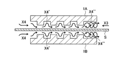
図1は、本発明の電気めっき装置の一実施の形態の模式図である。図示する電気めっき装置10は、電解槽2と、電解槽2内で金属帯Sを通板させる送り機構3と、電解槽2内で金属帯Sの通板方向(X3方向)と逆の方向(X4方向)にめっき液Mを噴流させる流通機構5と、金属帯Sを挟む位置に配設された一対の電極1A,1Bと、直流電源4とから大略構成されている。なお、同図において、金属帯Sが電極1A,1Bに入ってくる端部を入側、電気めっき処理された金属帯Sが電極1A,1Bから出て行く端部を出側としている。
FIG. 1 is a schematic view of an embodiment of an electroplating apparatus of the present invention. The illustrated
送り機構3を構成する送りローラは電極ローラとなっており(上ローラはX1方向回転、下ローラはX2方向回転)、直流電源4の陰極がこれに通じていて、送り機構3に接触する金属帯Sが陰極となり、めっきの金属陽イオンが金属帯Sの表面に電気めっきされるようになっている。
The feed roller constituting the
電解槽2内で金属帯Sの通板方向と逆方向に噴流されるめっき液Mには、ZnやNi、Sn,Cr、Cuなどの単一の純金属、Zn−Fe合金やZn−Ni合金、Zn−Ni−Co合金などの合金が用いられる。
The plating solution M that is jetted in the direction opposite to the plate passing direction of the metal strip S in the
図示する一対の電極1A,1Bはともに、対応する位置でかつ通板方向(X3方向)に凸部1bと凹部1aを交互に備えており、双方の電極1A,1Bの凸部1b、1b間で電極間距離が短くなり、双方の凹部1a,1a間で電極間距離が長くなっている。
The pair of
また、電極1A,1Bにおいて金属帯Sが入ってくる入側の端部には、複数の凹部の中でも通板方向長さの最も長い凹部1a’が配されている(ここでの通板方向長さs1>他の凹部1aの通板方向長さs2)。なお、この通板方向長さs1は、通板方向長さs2の1.5〜3倍程度の範囲に調整される。
In addition, a
なお、図示する電極1A,1Bは、入側端部の凹部1a’以外の凹部1aおよび凸部1bの通板方向長さが、同一長さs1となっている。
In the illustrated
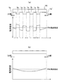
この電極1A,1Bに直流電源4から通電すると、図2aで示すように、平均電流密度に対して、凸部1b、1b間には相対的に高い電流密度域が形成され、凹部1a,1a間には相対的に低い電流密度域が形成され、直流電源からの通電にもかかわらず、パルス電流のごとき通電態様で異なる電流密度の電流が印加される。さらに、この電流密度分布は、電極の入側および出側から中央にむかってパルス状の電流密度が低くなるような電流密度分布を呈することになる。なお、図2bで示す従来構造の電極(電極表面が平坦)では、パルス状の電流密度分布が生じることはなく、電極の入側および出側から中央にむかって電流密度が低くなる二次曲線状を呈する。
When the
このようなパルス状の電流密度分布を呈する電極1A,1B間で金属帯Sを通板させ(X3方向)、この通板方向と逆向きにめっき液を噴流させると(X4方向)、図3で示すように、めっき液は電極表面の凹部1aと凸部1bを通過する過程でうねりながら噴流し(X4’方向)、最も長さの長い入側端部の凹部1a’では、うねりによってめっき液が攪拌される(X4”方向)。この攪拌により、金属帯表面への析出(めっき)によって消費され、減少した金属帯表面近傍のめっき液中の金属イオン濃度が均一化されためっき液が金属帯Sの表面に接触し、これによって金属板とめっき層の間の密着性が高まる。
When the metal strip S is passed between the
図示するように、電極1A,1Bが対応する凹部1a,1a’と凸部1bを交互に備えていることで、パルス電流を通電することなく、一つの電極1A,1B間で電解電流密度を変化させることができ、このことによって、電極間距離の短い対向する凸部1b、1b間には相対的に高電流密度域を形成してここで緻密な金属結晶を析出させ、電極間距離の長い対向する凹部1a,1a間(および凹部1a’,1a’間)には相対的に低電流密度域を形成してゆっくりと金属結晶を析出・成長させ、これらが交互に繰り返されることで、節状や樹枝状のめっき金属結晶を抑制することができる。このことは、1〜10m/分程度の低速で通板して電解する場合に、電解槽2中を金属帯Sが通過するのに長時間を要することから、仮に一定の電流密度で電解をおこなった場合には節状や樹枝状のめっき金属結晶の析出が顕著であることより、低速で金属帯を通板しながら電気めっきする際に本発明の装置の奏する効果は極めて大きい。
As shown in the figure, the
さらに、電極1A、1Bにおける金属帯Sの入側の端部に通板方向長さの最も長い凹部1a’を設けたことにより、図2aで示すように金属帯Sの表面におけるめっき初期の電流密度を低くすることができ、このことによってめっき金属の析出速度を抑制することができるとともに金属帯Sの表面におけるめっき液が上記するように十分に攪拌され、この攪拌されためっき液を金属帯Sに接触させることによって、金属帯Sとめっき金属が析出・成長してなるめっき層の間の密着性を高めることができる。
Further, by providing a
ここで、電極間における金属帯Sの通板位置と凹部1aの間の長さをLとした際に、凹部1aに対する凸部1bの金属帯側への突出長さhは、L/6〜L/3の範囲となっているのがよい。
Here, when the length between the plate position of the metal band S between the electrodes and the
凹部1aに対する凸部1bの金属帯S側への突出長さhがL/6よりも小さいと、電極1A,1B内における電流密度の変化が小さすぎてめっき液の攪拌効果や節状や樹枝状のめっき金属結晶抑制効果が少ないことが特定されている。一方、突出長さhがL/3よりも大きいと、対向する凸部1b、1b間の距離が小さくなり過ぎて接触の危険性が高まることが特定されている。
If the protrusion length h of the
また、同様に金属帯Sの通板位置と凹部1aの間の長さをLとした際に、凹部1a、1a’と凸部1bの通板方向長さがともに、2L〜10Lの範囲となっているのがよい。
Similarly, when the length between the plate passing position of the metal band S and the
凹部1a、1a’と凸部1bの通板方向長さがともに2Lよりも小さいと、電流密度の変化が小さ過ぎること、凹部1a、1a’と凸部1bの通板方向長さがともに10Lよりも大きいと、噴流するめっき液が一定電流密度内に留まる時間が長くなり過ぎることより、いずれも凹凸電極による効果が少なくなるためである。
If the lengths of the
また、電気めっきにおいて、電流密度が一定の値を超えると金属光沢のある正常なめっき層が得られず、たとえば亜鉛めっきなどでは黒みを帯びたいわゆる「ヤケ」が生じ、電流密度の増大にともなって電流効率が低下する恐れがある。ここで、限界電流密度:Dkに関しては以下の一般式が妥当する。 In addition, in electroplating, when the current density exceeds a certain value, a normal plating layer with a metallic luster cannot be obtained. For example, in zinc plating, black so-called “burning” occurs, and the current density increases. Current efficiency may be reduced. Here, the following general formula is valid for the limit current density: Dk.
![]()
![]()
ここで、Fはファラデー定数、Dは金属イオンの拡散係数(イオン固有の値)、Cは電解液中の金属イオン濃度(電解液の各種成分濃度によって制約があり、たとえば、薬剤の溶解度や組成による制約)、δは拡散層の厚さ(電解液の攪拌によって薄くできる)である。 Here, F is the Faraday constant, D is the diffusion coefficient of metal ions (values specific to ions), C is the metal ion concentration in the electrolyte solution (which is limited by the concentration of various components in the electrolyte solution, for example, the solubility and composition of the drug And δ is the thickness of the diffusion layer (which can be reduced by stirring the electrolyte).
凸部1b、1b間では、めっき液の流速が速くなるため、Dkが高くてもヤケは生じない。
Between the
また、凹部1a,1a間では、めっき液の流速が遅くなるが、Dkも低くなることから同様にヤケは生じない。このように、本発明の装置10を構成する電極1A,1Bを適用した場合であっても、めっきヤケの問題は生じ得ない。
Moreover, although the flow rate of a plating solution becomes slow between recessed
(電極の他の実施の形態)
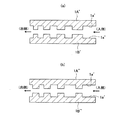
図4a,bはいずれも、電極の他の実施の形態を示す模式図である。
図4aで示す電極1A’、1B’は、金属帯Sが入ってくる入側の端部において通板方向長さの最も長い凹部1a’が配されている構成は図1で示す実施の形態と同様であるが、電極の入側の端部から出側の端部に向かって、それ以外の凹部と凸部がともにそれらの通板方向長さが漸次短くなっているものである。
(Other embodiments of electrode)
4a and 4b are schematic views showing other embodiments of electrodes.
The
また、図4bで示す電極1A”、1B”は、金属帯Sが入ってくる入側の端部において通板方向長さの最も長い凹部1a’が配されている構成は図1および図4aで示す実施の形態と同様であるが、電極の入側の端部から出側の端部に向かって、凹部の通板方向長さのみが漸次短くなっているものである。
Also, the
いずれの形態の電極であっても、金属帯Sとめっき金属が析出してなるめっき層の間の密着性を高めることができる。 Even if it is an electrode of any form, the adhesiveness between the metal belt | band | zone S and the plating layer in which a plating metal precipitates can be improved.
以上、本発明の実施の形態を図面を用いて詳述してきたが、具体的な構成はこの実施形態に限定されるものではなく、本発明の要旨を逸脱しない範囲における設計変更等があっても、それらは本発明に含まれるものである。 The embodiment of the present invention has been described in detail with reference to the drawings. However, the specific configuration is not limited to this embodiment, and there are design changes and the like without departing from the gist of the present invention. They are also included in the present invention.
1A、1A’、1A”、1B、1B’、1B”…電極、1a’… 入側端部の凹部、1a…凹部、1b…凸部、2…電解槽、3…送り機構(電極ローラ)、4…直流電源、5…流通機構、10…電気めっき装置、S…金属帯、M…めっき液 1A, 1A ′, 1A ″, 1B, 1B ′, 1B ″... Electrode, 1a ′... Concave portion at the entrance end, 1a... Concave portion, 1b. 4 ... DC power supply, 5 ... Distribution mechanism, 10 ... Electroplating device, S ... Metal strip, M ... Plating solution
Claims (6)
前記一対の電極はともに、対応する位置でかつ通板方向に凸部と凹部を交互に備え、双方の電極の凸部間で電極間距離が短くなり、双方の凹部間で電極間距離が長くなっており、
前記電極の金属帯が該電極に入ってくる入側の端部において、複数の凹部の中でも通板方向長さの最も長い凹部が配されている電気めっき装置。 An electrolytic cell, a feed mechanism for passing a metal band in the electrolytic cell, a flow mechanism for flowing a plating solution in the direction of the metal band in the electrolytic cell or in the opposite direction, and a position sandwiching the metal band An electroplating apparatus comprising a pair of electrodes provided,
Each of the pair of electrodes is provided with convex portions and concave portions alternately at corresponding positions and in the plate passing direction, the distance between the convex portions of both electrodes is shortened, and the distance between the two electrodes is long. And
An electroplating apparatus in which a recess having the longest length in the sheet passing direction is arranged among a plurality of recesses at an entrance end where the metal band of the electrode enters the electrode.
Priority Applications (1)
| Application Number | Priority Date | Filing Date | Title |
|---|---|---|---|
| JP2011064414A JP5676329B2 (en) | 2011-03-23 | 2011-03-23 | Electroplating equipment |
Applications Claiming Priority (1)
| Application Number | Priority Date | Filing Date | Title |
|---|---|---|---|
| JP2011064414A JP5676329B2 (en) | 2011-03-23 | 2011-03-23 | Electroplating equipment |
Publications (2)
| Publication Number | Publication Date |
|---|---|
| JP2012201889A true JP2012201889A (en) | 2012-10-22 |
| JP5676329B2 JP5676329B2 (en) | 2015-02-25 |
Family
ID=47183207
Family Applications (1)
| Application Number | Title | Priority Date | Filing Date |
|---|---|---|---|
| JP2011064414A Expired - Fee Related JP5676329B2 (en) | 2011-03-23 | 2011-03-23 | Electroplating equipment |
Country Status (1)
| Country | Link |
|---|---|
| JP (1) | JP5676329B2 (en) |
Citations (4)
| Publication number | Priority date | Publication date | Assignee | Title |
|---|---|---|---|---|
| JPH09235698A (en) * | 1996-02-29 | 1997-09-09 | Kawasaki Steel Corp | Electrolytic surface-clad electrode and method for continuously electroplating metallic strip using the electrode |
| JPH09279381A (en) * | 1996-04-16 | 1997-10-28 | Tdk Corp | Electrolytic electrode |
| JPH1072698A (en) * | 1996-08-30 | 1998-03-17 | Kawasaki Steel Corp | Electroplating device |
| JPH10102285A (en) * | 1996-09-26 | 1998-04-21 | Kawasaki Steel Corp | Electroplating device |
-
2011
- 2011-03-23 JP JP2011064414A patent/JP5676329B2/en not_active Expired - Fee Related
Patent Citations (4)
| Publication number | Priority date | Publication date | Assignee | Title |
|---|---|---|---|---|
| JPH09235698A (en) * | 1996-02-29 | 1997-09-09 | Kawasaki Steel Corp | Electrolytic surface-clad electrode and method for continuously electroplating metallic strip using the electrode |
| JPH09279381A (en) * | 1996-04-16 | 1997-10-28 | Tdk Corp | Electrolytic electrode |
| JPH1072698A (en) * | 1996-08-30 | 1998-03-17 | Kawasaki Steel Corp | Electroplating device |
| JPH10102285A (en) * | 1996-09-26 | 1998-04-21 | Kawasaki Steel Corp | Electroplating device |
Also Published As
| Publication number | Publication date |
|---|---|
| JP5676329B2 (en) | 2015-02-25 |
Similar Documents
| Publication | Publication Date | Title |
|---|---|---|
| Chandrasekar et al. | Pulse and pulse reverse plating—Conceptual, advantages and applications | |
| Tuaweri et al. | A study of process parameters for zinc electrodeposition from a sulphate bath | |
| CN106917039A (en) | A kind of cold rolling tin plate of flash plating and its manufacture method | |
| JPWO2020017655A1 (en) | Roughened nickel plated plate | |
| US20150354077A1 (en) | Electrodeposition of chromium from trivalent chromium using modulated electric fields | |
| CN101397691B (en) | Apparatus and technology for controlling and improving plating solution PH value on fingerprint resistant production chain | |
| US4249999A (en) | Electrolytic zinc-nickel alloy plating | |
| KR20160023927A (en) | High-strength, low-warping electrolytic copper foil and method for producing same | |
| KR900000283B1 (en) | Manufacturing method of zn-ni alloy plated steel strips | |
| CN101889107B (en) | Use the system and method for electroplating technology plating metal alloys | |
| JP5676329B2 (en) | Electroplating equipment | |
| Padhy et al. | Microstructural aspects of manganese metal during its electrodeposition from sulphate solutions in the presence of quaternary amines | |
| JPH0136559B2 (en) | ||
| US20150041326A1 (en) | Conductive metal enhanced with conductive nanomaterial | |
| EP3098334A1 (en) | Electrolytic process for coating metal surfaces to provide high wear resistance | |
| JP5747441B2 (en) | Method for producing electrogalvanized steel sheet | |
| Riastuti et al. | Effect of saccharin as additive in nickel electroplating on SPCC steel | |
| CN109628967B (en) | Nickel-cobalt alloy plating solution for crystallizer copper plate and device thereof | |
| US20040031694A1 (en) | Commercial process for electroplating nickel-phosphorus coatings | |
| JP2021085048A (en) | METHOD OF PRODUCING STEEL SHEET PLATED WITH Zn-Ni BASED ALLOY, AND ELECTROPLATING FACILITY | |
| JPS635474B2 (en) | ||
| JPS58161792A (en) | Horizontal electroplating method with alloy | |
| JP2009209419A (en) | Electrogalvanized steel having excellent color tone and method of manufacturing the same | |
| JP4256839B2 (en) | Electroplating electrode and electroplating method using the same | |
| JPS6215635B2 (en) |
Legal Events
| Date | Code | Title | Description |
|---|---|---|---|
| A621 | Written request for application examination |
Free format text: JAPANESE INTERMEDIATE CODE: A621 Effective date: 20131111 |
|
| A977 | Report on retrieval |
Free format text: JAPANESE INTERMEDIATE CODE: A971007 Effective date: 20140929 |
|
| A131 | Notification of reasons for refusal |
Free format text: JAPANESE INTERMEDIATE CODE: A131 Effective date: 20141007 |
|
| A521 | Written amendment |
Free format text: JAPANESE INTERMEDIATE CODE: A523 Effective date: 20141112 |
|
| TRDD | Decision of grant or rejection written | ||
| A01 | Written decision to grant a patent or to grant a registration (utility model) |
Free format text: JAPANESE INTERMEDIATE CODE: A01 Effective date: 20141202 |
|
| A61 | First payment of annual fees (during grant procedure) |
Free format text: JAPANESE INTERMEDIATE CODE: A61 Effective date: 20141225 |
|
| R150 | Certificate of patent or registration of utility model |
Ref document number: 5676329 Country of ref document: JP Free format text: JAPANESE INTERMEDIATE CODE: R150 |
|
| RD03 | Notification of appointment of power of attorney |
Free format text: JAPANESE INTERMEDIATE CODE: R3D03 |
|
| R250 | Receipt of annual fees |
Free format text: JAPANESE INTERMEDIATE CODE: R250 |
|
| R250 | Receipt of annual fees |
Free format text: JAPANESE INTERMEDIATE CODE: R250 |
|
| S533 | Written request for registration of change of name |
Free format text: JAPANESE INTERMEDIATE CODE: R313533 |
|
| R350 | Written notification of registration of transfer |
Free format text: JAPANESE INTERMEDIATE CODE: R350 |
|
| LAPS | Cancellation because of no payment of annual fees |