JP2012199411A - Light emitting device - Google Patents
Light emitting device Download PDFInfo
- Publication number
- JP2012199411A JP2012199411A JP2011062983A JP2011062983A JP2012199411A JP 2012199411 A JP2012199411 A JP 2012199411A JP 2011062983 A JP2011062983 A JP 2011062983A JP 2011062983 A JP2011062983 A JP 2011062983A JP 2012199411 A JP2012199411 A JP 2012199411A
- Authority
- JP
- Japan
- Prior art keywords
- light
- phosphor
- light emitting
- containing resin
- resin layer
- Prior art date
- Legal status (The legal status is an assumption and is not a legal conclusion. Google has not performed a legal analysis and makes no representation as to the accuracy of the status listed.)
- Granted
Links
- 239000011347 resin Substances 0.000 claims abstract description 167
- 229920005989 resin Polymers 0.000 claims abstract description 167
- OAICVXFJPJFONN-UHFFFAOYSA-N Phosphorus Chemical compound [P] OAICVXFJPJFONN-UHFFFAOYSA-N 0.000 claims description 139
- 239000000758 substrate Substances 0.000 claims description 81
- 239000002245 particle Substances 0.000 claims description 25
- 230000002093 peripheral effect Effects 0.000 claims description 12
- 238000007789 sealing Methods 0.000 claims description 10
- 239000004065 semiconductor Substances 0.000 claims description 7
- 239000012780 transparent material Substances 0.000 claims description 4
- 239000000463 material Substances 0.000 abstract description 14
- 230000005284 excitation Effects 0.000 abstract description 7
- 239000010410 layer Substances 0.000 description 161
- 230000000052 comparative effect Effects 0.000 description 16
- 239000011324 bead Substances 0.000 description 14
- 238000000034 method Methods 0.000 description 8
- 238000000926 separation method Methods 0.000 description 7
- 238000004519 manufacturing process Methods 0.000 description 5
- 108700042658 GAP-43 Proteins 0.000 description 4
- 238000006243 chemical reaction Methods 0.000 description 4
- 239000011248 coating agent Substances 0.000 description 4
- 238000000576 coating method Methods 0.000 description 4
- 238000005259 measurement Methods 0.000 description 4
- 239000000126 substance Substances 0.000 description 4
- 239000003795 chemical substances by application Substances 0.000 description 3
- 239000011521 glass Substances 0.000 description 3
- 229910004298 SiO 2 Inorganic materials 0.000 description 2
- 239000000853 adhesive Substances 0.000 description 2
- 230000001070 adhesive effect Effects 0.000 description 2
- 239000012790 adhesive layer Substances 0.000 description 2
- PNEYBMLMFCGWSK-UHFFFAOYSA-N aluminium oxide Inorganic materials [O-2].[O-2].[O-2].[Al+3].[Al+3] PNEYBMLMFCGWSK-UHFFFAOYSA-N 0.000 description 2
- 230000015572 biosynthetic process Effects 0.000 description 2
- 239000000919 ceramic Substances 0.000 description 2
- 239000004020 conductor Substances 0.000 description 2
- 238000002156 mixing Methods 0.000 description 2
- 239000004593 Epoxy Substances 0.000 description 1
- XUIMIQQOPSSXEZ-UHFFFAOYSA-N Silicon Chemical compound [Si] XUIMIQQOPSSXEZ-UHFFFAOYSA-N 0.000 description 1
- 229910052802 copper Inorganic materials 0.000 description 1
- 238000010586 diagram Methods 0.000 description 1
- 230000000694 effects Effects 0.000 description 1
- 238000005530 etching Methods 0.000 description 1
- 238000011156 evaluation Methods 0.000 description 1
- 230000012447 hatching Effects 0.000 description 1
- 230000017525 heat dissipation Effects 0.000 description 1
- 238000010438 heat treatment Methods 0.000 description 1
- 229910010272 inorganic material Inorganic materials 0.000 description 1
- 239000011147 inorganic material Substances 0.000 description 1
- 238000000691 measurement method Methods 0.000 description 1
- 238000002844 melting Methods 0.000 description 1
- 230000008018 melting Effects 0.000 description 1
- 239000002184 metal Substances 0.000 description 1
- 229910052751 metal Inorganic materials 0.000 description 1
- 230000003287 optical effect Effects 0.000 description 1
- 238000007517 polishing process Methods 0.000 description 1
- 229910052594 sapphire Inorganic materials 0.000 description 1
- 239000010980 sapphire Substances 0.000 description 1
- 229910052710 silicon Inorganic materials 0.000 description 1
- 239000010703 silicon Substances 0.000 description 1
- 229910052709 silver Inorganic materials 0.000 description 1
- 125000006850 spacer group Chemical group 0.000 description 1
- 230000003595 spectral effect Effects 0.000 description 1
- 238000004383 yellowing Methods 0.000 description 1
Images


Classifications
-
- H—ELECTRICITY
- H01—ELECTRIC ELEMENTS
- H01L—SEMICONDUCTOR DEVICES NOT COVERED BY CLASS H10
- H01L33/00—Semiconductor devices with at least one potential-jump barrier or surface barrier specially adapted for light emission; Processes or apparatus specially adapted for the manufacture or treatment thereof or of parts thereof; Details thereof
- H01L33/48—Semiconductor devices with at least one potential-jump barrier or surface barrier specially adapted for light emission; Processes or apparatus specially adapted for the manufacture or treatment thereof or of parts thereof; Details thereof characterised by the semiconductor body packages
- H01L33/50—Wavelength conversion elements
- H01L33/505—Wavelength conversion elements characterised by the shape, e.g. plate or foil
-
- H—ELECTRICITY
- H01—ELECTRIC ELEMENTS
- H01L—SEMICONDUCTOR DEVICES NOT COVERED BY CLASS H10
- H01L33/00—Semiconductor devices with at least one potential-jump barrier or surface barrier specially adapted for light emission; Processes or apparatus specially adapted for the manufacture or treatment thereof or of parts thereof; Details thereof
- H01L33/48—Semiconductor devices with at least one potential-jump barrier or surface barrier specially adapted for light emission; Processes or apparatus specially adapted for the manufacture or treatment thereof or of parts thereof; Details thereof characterised by the semiconductor body packages
- H01L33/58—Optical field-shaping elements
- H01L33/60—Reflective elements
-
- H—ELECTRICITY
- H01—ELECTRIC ELEMENTS
- H01L—SEMICONDUCTOR DEVICES NOT COVERED BY CLASS H10
- H01L2224/00—Indexing scheme for arrangements for connecting or disconnecting semiconductor or solid-state bodies and methods related thereto as covered by H01L24/00
- H01L2224/01—Means for bonding being attached to, or being formed on, the surface to be connected, e.g. chip-to-package, die-attach, "first-level" interconnects; Manufacturing methods related thereto
- H01L2224/42—Wire connectors; Manufacturing methods related thereto
- H01L2224/47—Structure, shape, material or disposition of the wire connectors after the connecting process
- H01L2224/48—Structure, shape, material or disposition of the wire connectors after the connecting process of an individual wire connector
- H01L2224/4805—Shape
- H01L2224/4809—Loop shape
- H01L2224/48091—Arched
-
- H—ELECTRICITY
- H01—ELECTRIC ELEMENTS
- H01L—SEMICONDUCTOR DEVICES NOT COVERED BY CLASS H10
- H01L2224/00—Indexing scheme for arrangements for connecting or disconnecting semiconductor or solid-state bodies and methods related thereto as covered by H01L24/00
- H01L2224/01—Means for bonding being attached to, or being formed on, the surface to be connected, e.g. chip-to-package, die-attach, "first-level" interconnects; Manufacturing methods related thereto
- H01L2224/42—Wire connectors; Manufacturing methods related thereto
- H01L2224/47—Structure, shape, material or disposition of the wire connectors after the connecting process
- H01L2224/48—Structure, shape, material or disposition of the wire connectors after the connecting process of an individual wire connector
- H01L2224/484—Connecting portions
- H01L2224/48463—Connecting portions the connecting portion on the bonding area of the semiconductor or solid-state body being a ball bond
- H01L2224/48465—Connecting portions the connecting portion on the bonding area of the semiconductor or solid-state body being a ball bond the other connecting portion not on the bonding area being a wedge bond, i.e. ball-to-wedge, regular stitch
-
- H—ELECTRICITY
- H01—ELECTRIC ELEMENTS
- H01L—SEMICONDUCTOR DEVICES NOT COVERED BY CLASS H10
- H01L25/00—Assemblies consisting of a plurality of individual semiconductor or other solid state devices ; Multistep manufacturing processes thereof
- H01L25/03—Assemblies consisting of a plurality of individual semiconductor or other solid state devices ; Multistep manufacturing processes thereof all the devices being of a type provided for in the same subgroup of groups H01L27/00 - H01L33/00, or in a single subclass of H10K, H10N, e.g. assemblies of rectifier diodes
- H01L25/04—Assemblies consisting of a plurality of individual semiconductor or other solid state devices ; Multistep manufacturing processes thereof all the devices being of a type provided for in the same subgroup of groups H01L27/00 - H01L33/00, or in a single subclass of H10K, H10N, e.g. assemblies of rectifier diodes the devices not having separate containers
- H01L25/075—Assemblies consisting of a plurality of individual semiconductor or other solid state devices ; Multistep manufacturing processes thereof all the devices being of a type provided for in the same subgroup of groups H01L27/00 - H01L33/00, or in a single subclass of H10K, H10N, e.g. assemblies of rectifier diodes the devices not having separate containers the devices being of a type provided for in group H01L33/00
- H01L25/0753—Assemblies consisting of a plurality of individual semiconductor or other solid state devices ; Multistep manufacturing processes thereof all the devices being of a type provided for in the same subgroup of groups H01L27/00 - H01L33/00, or in a single subclass of H10K, H10N, e.g. assemblies of rectifier diodes the devices not having separate containers the devices being of a type provided for in group H01L33/00 the devices being arranged next to each other
-
- H—ELECTRICITY
- H01—ELECTRIC ELEMENTS
- H01L—SEMICONDUCTOR DEVICES NOT COVERED BY CLASS H10
- H01L33/00—Semiconductor devices with at least one potential-jump barrier or surface barrier specially adapted for light emission; Processes or apparatus specially adapted for the manufacture or treatment thereof or of parts thereof; Details thereof
- H01L33/48—Semiconductor devices with at least one potential-jump barrier or surface barrier specially adapted for light emission; Processes or apparatus specially adapted for the manufacture or treatment thereof or of parts thereof; Details thereof characterised by the semiconductor body packages
- H01L33/50—Wavelength conversion elements
-
- H—ELECTRICITY
- H01—ELECTRIC ELEMENTS
- H01L—SEMICONDUCTOR DEVICES NOT COVERED BY CLASS H10
- H01L33/00—Semiconductor devices with at least one potential-jump barrier or surface barrier specially adapted for light emission; Processes or apparatus specially adapted for the manufacture or treatment thereof or of parts thereof; Details thereof
- H01L33/48—Semiconductor devices with at least one potential-jump barrier or surface barrier specially adapted for light emission; Processes or apparatus specially adapted for the manufacture or treatment thereof or of parts thereof; Details thereof characterised by the semiconductor body packages
- H01L33/62—Arrangements for conducting electric current to or from the semiconductor body, e.g. lead-frames, wire-bonds or solder balls
Abstract
Description
本発明は、発光素子からの光を波長変換層で変換する発光装置に関する。 The present invention relates to a light emitting device that converts light from a light emitting element with a wavelength conversion layer.
発光素子からの光の一部を蛍光体で異なる波長の光に変換し、発光素子からの光と混合して出射する発光装置が知られている。例えば、発光素子が青色光を発し、蛍光体が青色光の一部を黄色光に変換することにより、青色光と黄色光とが混合された白色光を放出することができる。 2. Description of the Related Art There is known a light emitting device that converts part of light from a light emitting element into light having a different wavelength with a phosphor, and mixes and emits the light from the light emitting element. For example, when the light emitting element emits blue light and the phosphor converts part of the blue light into yellow light, white light in which blue light and yellow light are mixed can be emitted.
特許文献1には、発光素子の上面に接着剤層を配置し、その上に板状の透光性部材を搭載した構成が開示されている。透光性部材には、蛍光体が含有されている。発光素子から出射される光は、透光性部材を通過する際に、一部蛍光に変換され、蛍光と発光素子から光が混合されて上方に放出される。特許文献1の構造では、発光素子および透光性部材の側面が光反射性樹脂で覆われ、側面に到達した発光素子からの光および蛍光を反射する。これにより、上面のみから光が出射されるため、高輝度の光を得ることができる。特許文献1には、光反射性樹脂を2段階に形成することにより、接着剤層で発光素子の側面が覆われないようにすることを提案している。 Patent Document 1 discloses a configuration in which an adhesive layer is disposed on an upper surface of a light emitting element, and a plate-like translucent member is mounted thereon. The translucent member contains a phosphor. The light emitted from the light emitting element is partially converted into fluorescence when passing through the translucent member, and the light is mixed from the fluorescence and the light emitting element and emitted upward. In the structure of Patent Document 1, the side surfaces of the light emitting element and the translucent member are covered with a light reflective resin, and light and fluorescence from the light emitting element that has reached the side surface are reflected. Thereby, since light is emitted only from the upper surface, high-luminance light can be obtained. Patent Document 1 proposes that a light-reflective resin is formed in two stages so that the side surface of the light-emitting element is not covered with an adhesive layer.
特許文献1のように、透光性部材を発光素子の上面に搭載し、周囲を光反射性部材で覆う構成は、透光性部材の端部で、色むらが生じるという問題がある。例えば、発光素子の発する光が青色で、蛍光が黄色である場合、青色光と黄色光とが混合された白色光が出射されるが、透光性部材の端部分で黄色みが強くなり、色むらが生じる。 As in Patent Document 1, a configuration in which a translucent member is mounted on the upper surface of a light-emitting element and the periphery is covered with a light-reflective member has a problem that uneven color occurs at the end of the translucent member. For example, when the light emitted from the light emitting element is blue and the fluorescence is yellow, white light in which blue light and yellow light are mixed is emitted, but the yellowing is enhanced at the end of the translucent member, Color unevenness occurs.
この原因の一つは、透光性部材の端面で、青色光および黄色光が反射される際、屈折率の波長依存性により青色光の反射角と黄色光の反射角とが異なり、黄色成分と青色成分とに分離するためである。また、別の原因としては、透光性部材の端面で光反射性樹脂により反射された青色光が、透光性部材内の蛍光体にて再び反射され、端面との間で多重反射することにより、透光性部材から出射するまでの光路長が長くなり、蛍光体により黄色蛍光に波長変換される確率が他の部分よりも大きくなるためである。 One of the causes is that when blue light and yellow light are reflected on the end face of the translucent member, the reflection angle of the blue light differs from the reflection angle of the yellow light due to the wavelength dependence of the refractive index, and the yellow component This is because it separates into a blue component. Another cause is that the blue light reflected by the light-reflective resin at the end face of the translucent member is reflected again by the phosphor in the translucent member and multiple-reflected between the end faces. This is because the optical path length until the light is emitted from the translucent member becomes longer, and the probability of wavelength conversion to yellow fluorescence by the phosphor becomes larger than that of other portions.
本発明の目的は、色むらの小さい発光装置を提供することにある。 An object of the present invention is to provide a light emitting device with small color unevenness.
上記目的を達成するために、本発明の第1の態様によれば、以下のような発光装置が提供される。すなわち、実装基板と、実装基板に搭載された発光素子と、発光素子上に配置された蛍光体含有樹脂層と、蛍光体含有樹脂層の上に搭載された透光性の板状部材とを有する発光装置であって、発光素子は、発光層を少なくとも含む1以上の半導体層である発光構造層と、発光構造層を支持する支持基板とを含む。板状部材の大きさは、発光構造層の大きさと同等以下であり、蛍光体含有樹脂層は、板状部材の端部から支持基板の端部を接続する傾斜した端面を備える。 In order to achieve the above object, according to the first aspect of the present invention, the following light emitting device is provided. That is, a mounting substrate, a light-emitting element mounted on the mounting substrate, a phosphor-containing resin layer disposed on the light-emitting element, and a translucent plate-shaped member mounted on the phosphor-containing resin layer The light emitting device includes a light emitting structure layer that is one or more semiconductor layers including at least a light emitting layer, and a support substrate that supports the light emitting structure layer. The size of the plate member is equal to or less than the size of the light emitting structure layer, and the phosphor-containing resin layer includes an inclined end surface that connects the end portion of the support substrate from the end portion of the plate member.
また、本発明の第2の態様によれば、以下のような発光装置が提供される。すなわち、実装基板と、実装基板に搭載された発光素子と、発光素子上に配置された蛍光体含有樹脂層と、蛍光体含有樹脂層の上に搭載された透光性の板状部材とを有する発光装置であって、発光素子は、発光層を少なくとも含む1以上の半導体層である発光構造層と、発光構造層を支持する支持基板とを含む。板状部材の大きさは、発光構造層の大きさと同等以下であり、蛍光体含有樹脂層の端面は、板状部材の側面よりも外周側に位置する。 Moreover, according to the 2nd aspect of this invention, the following light-emitting devices are provided. That is, a mounting substrate, a light-emitting element mounted on the mounting substrate, a phosphor-containing resin layer disposed on the light-emitting element, and a translucent plate-shaped member mounted on the phosphor-containing resin layer The light emitting device includes a light emitting structure layer that is one or more semiconductor layers including at least a light emitting layer, and a support substrate that supports the light emitting structure layer. The size of the plate member is equal to or less than the size of the light emitting structure layer, and the end surface of the phosphor-containing resin layer is located on the outer peripheral side of the side surface of the plate member.
発光構造層の端部の直上における蛍光体含有樹脂層の膜厚は、蛍光体含有樹脂層に含有される蛍光体粒子の粒径よりも大きいことが望ましい。また、蛍光体含有樹脂層の端面は、支持基板の法線との成す角が、60度以内であることが望ましい。板状部材の一辺の大きさは、発光構造層の対応する一辺の大きさとの差が50μm以内であることが望ましい。 The film thickness of the phosphor-containing resin layer immediately above the end of the light emitting structure layer is desirably larger than the particle size of the phosphor particles contained in the phosphor-containing resin layer. Moreover, it is desirable that the end surface of the phosphor-containing resin layer has an angle formed with the normal line of the support substrate within 60 degrees. The size of one side of the plate-like member is preferably 50 μm or less with respect to the size of the corresponding side of the light emitting structure layer.
発光構造層の上面には電極が配置された構造である場合、電極上には、電極とボンディングワイヤとの接続部を封止する封止樹脂が配置された構成にすることができる。 In the case where an electrode is disposed on the upper surface of the light emitting structure layer, a sealing resin for sealing a connection portion between the electrode and the bonding wire can be disposed on the electrode.
蛍光体含有樹脂層の端面および板状部材の端面に対して所定の間隙をあけて対向する光反射性樹脂層を配置することが可能である。この間隙は、発光素子の発する光に対して透明な透明材料により充填することが可能である。 It is possible to dispose a light-reflective resin layer facing the end face of the phosphor-containing resin layer and the end face of the plate-like member with a predetermined gap. This gap can be filled with a transparent material that is transparent to the light emitted from the light emitting element.
本発明によれば、蛍光体含有樹脂層の端面から、板状部材の外側を通して一部の光を出射することができるため、この光を、板状部材の端部で波長分離した光と混合することにより、色むらを低減できる。 According to the present invention, since a part of light can be emitted from the end face of the phosphor-containing resin layer through the outside of the plate-like member, this light is mixed with the light wavelength-separated at the end of the plate-like member. By doing so, color unevenness can be reduced.
以下、本発明の一実施の形態の発光装置について説明する。 Hereinafter, a light emitting device according to an embodiment of the present invention will be described.
本発明では、蛍光体含有樹脂層の上に板状の透明部材を配置する構成であるが、一部の励起光を蛍光体含有樹脂層の端面から上方に向かって、透明部材を通さず直接出射する構成とする。これにより、透明部材の端面付近から多く出射される蛍光と、蛍光体含有樹脂層の端面から透明部材を通さずに直接出射された励起光とを混合し、透明部材の端面付近における色むらを低減する。 In the present invention, a plate-like transparent member is disposed on the phosphor-containing resin layer, but a part of the excitation light is directly directed upward from the end face of the phosphor-containing resin layer without passing through the transparent member. It is set as the structure which radiate | emits. As a result, a large amount of fluorescence emitted from the vicinity of the end face of the transparent member is mixed with excitation light directly emitted from the end face of the phosphor-containing resin layer without passing through the transparent member, and color unevenness in the vicinity of the end face of the transparent member is reduced. To reduce.
(第1の実施形態)
図1に、第1の実施形態の発光装置を示す。図1(a)は上面図、図1(b)、(c)は、それぞれA−A断面図、B−B断面図である。なお、図の理解を容易にするために図1(a)の上面図にもハッチングを付している。
(First embodiment)
FIG. 1 shows a light emitting device according to the first embodiment. 1A is a top view, and FIGS. 1B and 1C are an AA sectional view and a BB sectional view, respectively. In order to facilitate understanding of the drawing, the top view of FIG. 1A is also hatched.
上面に電極および配線が形成された実装基板10の上に、LED素子11が実装されている。LED素子11は、半導体をエピタキシャル成長させた発光層を含む発光構造体(以下、エピ層)12と、これを支持する支持基板13とを備えている。エピ層12の上面形状は、支持基板13の上面形状よりもわずかに小さい。エピ層12の端面は、支持基板13の端面よりも数十ミクロン(<100μm)内側、例えば50μm程度内側に位置することが望ましい。
An
エピ層12は、発光層の他に、発光層をエピタキシャル成長させる際に用いた成長基板を含んでいてもよい。エピ層12は、メタルボンディングにより支持基板13に固定されている。
In addition to the light emitting layer, the
支持基板13は、エピ層の発する発光波長に対して不透明で、かつ、導電性の材料により構成されている。支持基板13の下面には、アノード電極(不図示)が配置されている。実装基板10には、支持基板13と接する部分に電極が備えられており、支持基板13のアノード電極と導電性のダイアタッチ剤により接続されている。
The
エピ層12の上面形状は矩形であり、隣り合う二つの角部には、一対のカソード電極15が配置されている。一対のカソード電極15は、実装基板10上のボンディング用電極パターン16にボンディングワイヤ17により接続されている。
The top surface shape of the
LED素子11の上面には、蛍光体含有樹脂層14が配置されている。蛍光体含有樹脂層14は、LED素子11の発する光(励起光)を吸収して励起され、所定波長の蛍光を発する蛍光体を、透明樹脂に分散させた材料により構成されている。透明樹脂は、LED素子11の発する励起光および蛍光に対して透明である。蛍光体含有樹脂層14には、蛍光体含有樹脂層14の膜厚を一定にするスペーサーとなる透明ビーズを分散させることも可能である。
A phosphor-containing
蛍光体含有樹脂層14は、LED素子11のエピ層12の上面および端面を覆うように、支持基板13の上面全体に配置されている。蛍光体含有樹脂層14の端面形状は、外向きに凸の湾曲面もしくは傾斜面となっている。この端面形状の詳細については後述する。
The phosphor-containing
蛍光体含有樹脂層14の上には、板状の透明部材18が搭載されている。透明部材18の上面形状は、図2に示すように、エピ層12の上面形状と対応した矩形であって、カソード電極15に対応する部分に切り欠き19を備えた形状である。
A plate-shaped
透明部材18の矩形の2辺の長さa,bは、エピ層12の対応する2辺の長さA,Bと同等もしくはそれ以下(a≦A、b≦B)に設定されている。透明部材18の2辺の長さa,bは、エピ層12の2辺の長さA,Bよりも小さい場合、その差が50μm以内であることが望ましい。すなわち、(A−50μm)≦a≦A、(B−50μm)≦b≦Bであることが望ましい。
The lengths a and b of the two sides of the rectangle of the
切り欠き19の2辺の長さc、dは、カソード電極15の対応する2辺の長さC、Dと同程度か数十μm(例:50μm)程度大きいことが望ましい。
The lengths c and d of the two sides of the
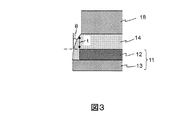
蛍光体含有樹脂層14の端面形状は、図3に示したように、透明部材18の端部から支持基板13の端部を接続する傾斜した形状である。よって、エピ層12の端部における蛍光体含有樹脂層14の膜厚tは、透明部材18直下の蛍光体含有樹脂層14の膜厚と同等かそれよりも薄い。膜厚tは、蛍光体粒子の平均粒径以上であることが望ましい。本願における蛍光体の平均粒径は、レーザー回折式の測定方法にて、体積基準で粒径分布の測定結果から50%時の粒径とする。これにより、エピ層12の端部の上部に蛍光体粒子を配置することができるため、エピ層12の上面の端部近傍から出射される光の一部を蛍光体粒子に入射させ、蛍光に変換することが可能になるためである。また、蛍光体含有樹脂層14の端面形状は、エピ層12の上面よりも上の部分が支持基板13の法線に対して成す角θが60度以下の急峻なテーパー形状であることが望ましい。急峻なテーパー形状とすることにより、エピ層12の端部近傍での蛍光体含有樹脂層14の膜厚を厚く確保することができるためである。
As shown in FIG. 3, the end surface shape of the phosphor-containing
以下、各層材質等について具体例に説明する。エピ層12としては、ここでは公知の青色光を発するGaN等の発光層を含むものを用いる。実装基板10の材質は、放熱効果の高い、高熱伝導材質の部材を用いることが望ましく、例えば、アルミナやセラミック製の実装基板や、スルーホール構造を有するガラスエポキシ基板等(スルーホールの部材は、Cu、Agからなる部材など)を用いる。また、LED素子11を実装するダイアタッチ剤としては、融点よりが高く、高熱伝導性も高い材質であることが望ましく、例えばAuSnを用いる。
Hereinafter, each layer material etc. are demonstrated to a specific example. As the
蛍光体含有樹脂層14の基材となる透明樹脂は、シリコン樹脂を、蛍光体としては青色光を励起光として黄色光を発する蛍光体(例えばYAG蛍光体)を用いることができる。例えば、平均粒径が約12μmの蛍光体を、透明樹脂に対して、20〜30wt%で分散したものを用いることができる。蛍光体含有樹脂層14の膜厚を決定するために透明ビーズを混合する場合には、粒径が所望の膜厚のビーズを用いる。このとき、蛍光体粒子は、粒径がビーズよりも小さいものを用いる。例えば、Φ30μmからΦ50μm程度の粒径のビーズを使用する。ビーズの材質は、蛍光体含有樹脂層14の基材の透明樹脂の屈折率nと屈折率が同等(n±0.2)のものが好ましく、例えば、SiO2、アルミナ等の透明材料からなるビーズを用いる。また、ビーズが、蛍光体を含有する透明材料から構成されていてもよい。これにより、ビーズからも蛍光が発せられ、ビーズの部分で蛍光色が抜ける現象を防止できる。
As the transparent resin serving as the base material of the phosphor-containing
ビーズを蛍光体含有樹脂層14に混合しない場合には、蛍光体粒子の最大粒径が蛍光体含有樹脂層14の膜厚を決定するので、最大粒径が所望の膜厚に一致する蛍光体粒子を用いる。
When the beads are not mixed with the phosphor-containing
透明部材18の材質は、無機材料であっても樹脂であっても構わないが、蛍光体含有樹脂14の屈折率と同等かそれ以下であることが望ましい。透明部材18が蛍光体含有樹脂14よりも高い屈折率の材質を用いた場合、蛍光体含有樹脂14および蛍光体含有樹脂14に分散されたビーズと透明部材18との界面で、光の反射が生じて取り出し効率が低下してしまうからである。例えば、透明部材18の材質としては、SiO2からなる一般的なガラス材質や、サファイアなどを用いる。透明部材18は、研磨工程と、ダイシングソーを用いたダイシング工程を経て形成することができる。他の方法としては、レーザーダイシング、エッチング等による形成方法もある。
The material of the
また、透明部材18に蛍光体粒子を分散させることも可能である。また、透明部材18として蛍光セラミックや蛍光ガラスを用いることも可能である。
It is also possible to disperse phosphor particles in the
本実施形態の発光装置の各部の作用について図4(a)、(b)を用いて説明する。また、比較例1を図4(c)を用いて説明する。 The operation of each part of the light emitting device of this embodiment will be described with reference to FIGS. Comparative Example 1 will be described with reference to FIG.
まず、図4(a)のように、本実施形態の、透明部材18の一辺a、bと、それに対応するエピ層12の一辺A、Bのサイズの関係が、A−50μm≦a≦A、B−50μm≦b≦Bである場合について説明する。
First, as shown in FIG. 4A, the size relationship between the sides a and b of the
支持基板13の裏面電極およびエピ層12のカソード電極15に、実装基板10の電極から所定の電圧を印加すると、エピ層12中の発光層から青色光が発せられる。青色光は、蛍光体含有樹脂層14に入射し、一部は蛍光体に吸収され黄色の蛍光に変換され、変換されなかった青色光と混合されて白色光となり、蛍光体含有樹脂層14の上面から透明部材18の底面に入射する。透明部材18の底面に入射した白色光の多くは、透明部材18を透過し、透明部材18の上面に到達して透明部材18の上面から白色光40として出射される。
When a predetermined voltage is applied from the electrode of the mounting
透明部材18の底面に入射した白色光の一部は、透明部材18の端面に到達し、端面で反射されて上面に向かう。このとき、透明部材18の屈折率の波長依存性により、白色光はスペクトル強度の高い黄色光41と青色光42に分離され、黄色光41の反射角が青色光42の反射角よりも大きいため、透明部材18の上面の端部近傍からは黄色光41が多くから出射される。この黄色光41が周りの白色光40との色度差があるため、このままでは色ムラと認識される。
Part of the white light incident on the bottom surface of the
本実施形態では、透明部材18の大きさを、上述のようにエピ層12と同等以下となるように設計しているため、透明部材18よりも外周に蛍光体含有樹脂層14の傾斜した端面が位置する。透明部材18よりも外周側に位置する蛍光体含有樹脂層14の膜厚は、透明部材18の直下の蛍光体含有樹脂層14の膜厚よりも薄いため、透明部材18よりも外周側に位置する蛍光体含有樹脂層14に含有される蛍光体量は、透明部材18直下の領域よりも少なく、黄色光への変換効率は透明部材18直下の領域よりも低い。このため、透明部材18の外周側に位置する蛍光体含有樹脂層14の端面からは、青色成分の多い、青白光43が出射される。
In the present embodiment, since the size of the
本実施形態では、透明部材18の大きさを、上述のようにエピ層12と同等以下となるように設計しているため、エピ層12の端部の直上における蛍光体含有樹脂層14の膜厚は、蛍光体含有樹脂層に含有される蛍光体粒子の平均粒径よりも大きく設定しやすく、蛍光体含有樹脂層の最大膜厚(透明部材直下の蛍光体含有樹脂層の膜厚)の1/2以上に設定しやすいものとなっている。
In the present embodiment, since the size of the
この青白光43が、透明部材18の外周に沿って上方に向かって出射されることにより、前述の色分離により生じた黄色光41と混合され、ほぼ白色光となる。よって、本実施形態では、透明部材18の端部においても、白色光を出射することができ、色むらのない発光装置を提供できる。
The blue-
また、図4(b)のように、透明部材18の大きさがエピ層12よりも小さい(a<A−50μm、b<B−50μm)場合、透明部材18よりも外周に位置する蛍光体含有樹脂層14の端面の出射面積が増加する。また、蛍光体含有樹脂層14の端面部分の膜厚が、図4(a)の場合と比較して薄くなるため、端面から出射される青白光44は、図4(a)の端面から出射される青白光43よりも青色成分が増加する。
Further, as shown in FIG. 4B, when the
このため、透明部材18の端面での色分離により生じた黄色光41と青白光43が混合された場合に、図4(a)の場合より青色成分が強い白色光となるが、黄色光41がそのまま出射される図4(c)の比較例1と比較すると色むらを抑制できる。
For this reason, when the
比較例1は、図4(c)のように透明部材18をエピ層12よりも大きくした(a>A、b>B)場合を示す。この場合、透明部材18よりも外側に蛍光体含有樹脂層14の傾斜した端面が位置しないため、透明部材18よりも外側から蛍光体含有樹脂層14の光が直接出射されることはない。よって、透明部材18の端面での色分離により生じた黄色光41がそのまま出射されるため、透明部材18の端部近傍からの出射光が黄色みを帯び、色むらを生じる。
Comparative Example 1 shows a case where the
以上のように、本実施形態では、エピ層12と同等以下の大きさの透明部材18を蛍光体含有樹脂層14の上に搭載し、透明部材18よりも外周側に蛍光体含有樹脂層14の傾斜した端面を位置させることにより、透明部材18の端部分とそれ以外の部分の色度差による色ムラを改善した発光装置が提供可能となる。
As described above, in this embodiment, the
<製造方法>
次に、本実施形態の発光装置の製造方法について説明する。
<Manufacturing method>
Next, a method for manufacturing the light emitting device of this embodiment will be described.
まず、LED素子11の支持基板13の裏面電極を実装基板10にダイアタッチ剤を用いて実装する。
First, the back electrode of the
一対のカソード電極15を第1ボンディング側とし、実装基板10の電極パターン16側を第2ボンディング側にしてワイヤーボンディングを行う。ボンディングワイヤ17のループトップは、LED素子11上面から大きく離れない位置、例えば100μmから200μmに位置するようにする。なお、第1および第2ボンディングの順番は逆にすることも可能である。
Wire bonding is performed with the pair of
つぎに、未硬化の樹脂に、蛍光体および、必要に応じてビーズを混合して分散させて未硬化の蛍光体含有樹脂を用意し、LED素子11の上面に、ディスペンサーにて所定量を塗布する。ディスペンサーの他、印刷等により行っても良い。塗布量によって、完成後の蛍光体含有樹脂層14の傾斜面の形状を制御することができる。
Next, a phosphor and, if necessary, beads are mixed and dispersed in an uncured resin to prepare an uncured phosphor-containing resin, and a predetermined amount is applied to the upper surface of the
予め用意しておいた所定形状の透明部材18を未硬化の蛍光体含有樹脂の上面に接するように搭載する。これにより、透明部材18の重さで、未硬化の蛍光体含有樹脂が、エピ層12の全面と側面を多い、支持基板13の上面の端部まで濡れ広がると同時に、透明部材18の直下は、未硬化の蛍光体含有樹脂の膜厚がビーズまたは蛍光体粒子にてレベリングされ、膜厚が決定される。さらに、透明部材18の各辺は、未硬化の蛍光体含有樹脂の表面張力によって、支持基板13の対応する各辺と平行になるように移動し、セルフアライメントされる。これにより、透明部材18の位置は、支持基板13の中央に収まり、位置ずれはほとんど生じない。同時に、透明部材18の大きさと支持基板13の大きさの関係および蛍光体含有樹脂の塗布量により、蛍光体含有樹脂層の端面の形状が決定される。これにより、端面が急峻なテーパー形状の蛍光体含有樹脂層を形成できる。
A
なお、エピ層12の側面から支持基板13の側面までの距離が100μm以上ある場合は、蛍光体含有樹脂の塗布工程前に、カソード電極周囲以外の支持基板13周囲に透明樹脂で囲いを形成しておくことで、蛍光体含有樹脂をせき止めることも可能である。これにより、急峻なテーパー状の端面を有する蛍光体含有樹脂層を形成することができる。
In addition, when the distance from the side surface of the
透明部材18を配置した後、所定の硬化工程により蛍光体含有樹脂層14をその形状を保ったまま硬化させる。硬化工程としては、例えば、150度にて4時間程度加熱する工程を用いる。以上により、本実施形態の発光装置が完成する。
After disposing the
(第2の実施形態)
第2の実施形態の発光装置を図5(a),(b),(c)を用いて説明する。図5(a)は、第2の実施形態の発光装置の上面図、図5(b)はC−C断面図、図5(c)はD−D断面図である。
(Second Embodiment)
The light emitting device of the second embodiment will be described with reference to FIGS. 5 (a), 5 (b), and 5 (c). FIG. 5A is a top view of the light emitting device according to the second embodiment, FIG. 5B is a CC cross-sectional view, and FIG. 5C is a DD cross-sectional view.
第2の実施形態では、カソード電極15にボンディングワイヤ17を第1ボンディンする際に形成されたボンディングボール及びその周辺ワイヤー17を封止するように、封止樹脂19を配置した。それ以外の構造は、第1の実施形態と同じ構造である。封止樹脂19としては、透明樹脂または白色樹脂(光反射性の粒子を混合した透明樹脂)を用いる。
In the second embodiment, the sealing
この封止樹脂19を配置することで、蛍光体含有樹脂層14がカソード電極15、ボールおよびその周辺ワイヤー17に接しない。このため、エピ層12から出射された光が、カソード電極15、ボールおよびその周辺ワイヤー17の周囲で反射され、この反射光が蛍光体粒子との間で多重反射されることがなく、多重反射により黄色蛍光に高効率で変換されて色むらが生じるのを防止することができる。
By disposing the sealing
よって、第2の実施形態では、透明部材18の端部における色むらを防止できるとともに、カソード電極15周辺部における色むらも防止できる。
Therefore, in the second embodiment, color unevenness at the end of the
第2の実施形態の発光装置の製造方法は、ワイヤーボンディング工程後に、カソード電極15上にボンディングボールを封止するように封止樹脂を塗布し、硬化させる工程を追加する。カソード電極15から封止樹脂が流れ出さないように、粘度が高い樹脂を用いて行うことが望ましい。その後、蛍光体含有樹脂層を塗布する工程を行う。他の工程は、第1の実施形態と同じである。
In the method of manufacturing the light emitting device according to the second embodiment, after the wire bonding step, a step of applying and sealing a sealing resin on the
(第3の実施形態)
第3の実施形態の発光装置を図6(a)を用いて説明する。
(Third embodiment)
A light emitting device according to a third embodiment will be described with reference to FIG.
第3の実施形態では、図6(a)のように蛍光体含有樹脂層14の端面および透明部材18の端面の外周側に、所定の間隔の間隙64を挟んで光反射性樹脂層61を配置する。光反射性樹脂層61は、蛍光体含有樹脂層14の端面および透明部材18の端面と対向する面は、支持基板13の法線と平行な壁面(垂直壁面)である。支持基板13の側面は、光反射性樹脂層61と接していることが望ましい。間隙64内は、透明樹脂が充填されていてもよいし、空隙であってもよい。
In the third embodiment, as shown in FIG. 6A, the light-
第3の実施形態においても、蛍光体含有樹脂層14の端面および透明部材18の端面と、光反射樹脂層61の垂直壁面との間に間隙64が形成されているため、第1の実施形態と同様、蛍光体含有樹脂層14の端面から上方に向けて出射された青白光は、間隙64を通過して、垂直壁面に妨げられずに上方から出射できる。このため、青白光42が、透明部材18の端面で分離して生じた黄色光41と混合されて白色光となり、透明部材18の端部で色むらが生じるのを防止できる。
Also in the third embodiment, since the gap 64 is formed between the end face of the phosphor-containing
光反射性樹脂層61を配置したことにより、蛍光体含有樹脂層14の内部で蛍光と青色光が混合されて生じた白色光のうち、蛍光体含有樹脂層14の端面から横方向に出射された光62は、光反射性樹脂層61により反射して蛍光体含有樹脂層14や透明部材18内に戻り、一部を透明部材18の上面から出射することができる。よって、側面からの放射光を上面から出射できるため、透明部材18の上面の輝度を向上させることができる。
By disposing the light-reflecting
一方、光反射性樹脂層61により反射されて蛍光体含有樹脂層14に戻った光の一部は、蛍光体との間で多重反射して黄色光63を生じ、この黄色光63が蛍光体含有樹脂層14の端面から上方へ出射されるが、この黄色光63は色むらを生じさせない。その理由は、第1に、多重反射により生じる黄色光63は、蛍光体含有樹脂層14の端面付近の膜厚が透明部材18直下よりも薄く、蛍光体量の少ないことから、光量が小さい。第2に、蛍光体含有樹脂層14の端面および透明部材18の端面と、光反射樹脂層61の垂直壁面との間に間隙64を形成しているため、第1の実施形態で説明した蛍光体含有樹脂層14の端面から上方に向けて出射される青白光43は、間隙64を通過し、垂直壁面に妨げられずに上方から出射できる。このため、青白光43が、多重反射で生じた黄色光63および透明部材18の端面で分離して生じた黄色光41と混合されて、白色光となる。これにより、透明部材18の端部で、色むらが生じるのを防止できる。
On the other hand, part of the light reflected by the light-reflecting
第3の実施形態の発光装置の製造方法について説明する。まず、第1の実施形態の製造方法と同様に、LED素子11の支持基板13の裏面を実装基板10にダイスボンディングする。つぎに、光反射性樹脂61で構成されたリングを支持基板13の外周に、エピ層12に対して間隙64が生じるように配置し、リングを実装基板10上に接着剤により固定する。リングは、光反射性樹脂61により予め成型されたものを用いてもよいし、ディスペンサー等で光反射性樹脂61を実装基板10上に塗布することにより形成してもよい。その後、第1の実施形態と同様にワイヤーボンディング工程と、未硬化の蛍光体含有樹脂層14の塗布工程、透明部材18の搭載工程および蛍光体含有樹脂層14の硬化工程を行う。次に、光反射性樹脂61のリングと、蛍光体含有樹脂層14および透明部材18の端面との間隙64に、蛍光体含有樹脂層14および透明部材18の端面と密着するように透明樹脂をディスペンサー等で塗布する。
A method for manufacturing the light emitting device of the third embodiment will be described. First, similarly to the manufacturing method of the first embodiment, the back surface of the
間隙64を空隙とする場合には、予め光反射樹脂で成形しておいた光反射性樹脂61を、蛍光体含有樹脂層14および透明部材18の端面と対向させて配置し、実装基板10に接着剤等で固定する。
When the gap 64 is used as a gap, a light-reflecting
比較例2として、図6(b)に示すように、蛍光体含有樹脂層14の端面および透明部材18の端面と密着するように光反射性樹脂61を配置した場合について説明する。
As Comparative Example 2, a case where the light-reflecting
比較例2の構造の場合には、蛍光体含有樹脂層14の端面および透明部材の端面から横方向に出射される白色光が、光反射性樹脂61により反射されて戻り光となり、透明部材18の上面の輝度は大きくなる。このとき屈折率の波長依存性により、黄色光と青色光に分離されるため、透明部材18の端部には黄色光41が生じる。また、戻り光が蛍光体含有樹脂層14により黄色蛍光に反射されるため、透明部材18の上面にはさらに黄色光65が到達する。よって、透明部材18全体で黄色光41、65が増加する。透明部材18の中央部は、輝度が大きく、光反射性樹脂61の有無のみで異なる同様の構成を有する第3の実施形態と比較して、黄色成分の多い白色光となる。
In the case of the structure of Comparative Example 2, the white light emitted in the lateral direction from the end face of the phosphor-containing
蛍光体含有樹脂層14の端面が光反射性樹脂61によって覆われているため、本実施形態のように端面から上方に向けて青白光43は出射されない。このため、反射時の分離により生じた黄色光41を白色光にすることができない。
Since the end surface of the phosphor-containing
したがって、比較例2の構造では、透明部材18の上面全体で黄色成分の多い白色光となり、端部分では黄色光41により黄色光が強くなる。したがって、比較例2の構成では色むらを改善することができない。
Therefore, in the structure of Comparative Example 2, the entire upper surface of the
比較例3として、図6(c)に示すように、特許文献1のようにフリップチップ型の発光素子161の上面に透明樹脂162により蛍光板163を接着し、蛍光板163の端面を光反射性樹脂164により覆った構成を示す。
As Comparative Example 3, as shown in FIG. 6C, as shown in Patent Document 1, a
比較例3の構造では、発光素子161からの青色光は、蛍光板163に入射し、一部が黄色蛍光に変換され、白色光を生じ、上面から出射される。蛍光板163の端面では、光反射性樹脂164により白色光が反射される。この際、屈折率の波長依存性により青色光の反射角と黄色光の反射角とが異なるため、蛍光板163の端部分から黄色光41が出射される。また、蛍光板163の端面で光反射性樹脂164により反射された青色光が、蛍光体との間で多重反射することにより、黄色光66に変換される。このため、蛍光板163の端部分では、黄色光41、66により黄色みの強い光が出射される。蛍光板の中心部分からは白色光が出射される。よって、蛍光板163の中心部分と端部分とで色むらが生じる。
In the structure of Comparative Example 3, blue light from the
(第4の実施形態)
第4の実施形態の発光装置を図7(a),(b)を用いて説明する。図7(a)は上面図、図7(b)はE−E断面図であるが、図の理解を容易にするために図7(a)においてもハッチングを付している。
(Fourth embodiment)
A light emitting device according to a fourth embodiment will be described with reference to FIGS. FIG. 7A is a top view and FIG. 7B is an EE cross-sectional view, but hatching is also provided in FIG. 7A for easy understanding of the drawing.
第4の実施形態の発光装置は、第1の実施形態の発光装置のLED素子11に代えてフリップチップ型のLED素子111を用いるものである。このLED素子111は、成長基板113の下面側に、発光層を含むエピ層12を成長させたものである。成長基板113は、エピ層12が発する光に透明である。
The light emitting device of the fourth embodiment uses a flip chip
エピ層12の下面には、アノード電極とカソード電極(不図示)が配置されている。LED素子11は、成長基板113を上方に向け、エピ層12を実装基板10側に向けて実装基板10にバンプ117を用いて実装されている。実装基板10の上面には、蛍光体含有樹脂層14の形成領域を定めるための段差部10aが設けられ、段差部10a上に一対の電極パターン116が配置されている。LED素子111のアノード電極とカソード電極は、一対の電極パターン116とバンプ117により接続されている。
An anode electrode and a cathode electrode (not shown) are disposed on the lower surface of the
蛍光体含有樹脂層14は、成長基板113と透明部材118との間のみならず、しかも、蛍光体含有樹脂層14は、成長基板113とエピ層12の側面を被覆し、エピ層12と実装基板10との間隙も充填するように形成されている。蛍光体含有樹脂層14が形成されている実装基板10上の領域は、段差部10aと一致している。
The phosphor-containing
第4の実施形態の発光装置においても、透明部材18の矩形の2辺の長さa,bは、エピ層12の対応する2辺の長さA,Bと同等もしくはそれ以下(a≦A、b≦B)に設定されている。透明部材18の2辺の長さa,bは、エピ層12の2辺の長さA,Bよりも小さい場合、その差が50μm以内であることが望ましい。すなわち、(A−50μm)≦a≦A、(B−50μm)≦b≦Bであることが望ましい。
Also in the light emitting device of the fourth embodiment, the lengths a and b of the rectangular two sides of the
また、蛍光体含有樹脂層14の端面形状は、エピ層12の上面よりも上に位置する部分が支持基板13の法線に対して成す角θが60度以下の急峻なテーパー形状であることが望ましい。他の構成は、第1の実施形態と同様であるので説明を省略する。
Further, the end face shape of the phosphor-containing
エピ層12から出射された光は、成長基板113を通って上方に向かい、蛍光体含有樹脂層14で一部が黄色光に波長変換され、透明部材18から出射される。このとき、透明部材18の側面で白色光が反射される際に色分離が生じ、透明部材の端部付近からは黄色光が出射されるが、第1の実施形態と同様に、透明部材18の外側に位置する蛍光体含有樹脂層14の傾斜した端面から青白光が出射されるため、黄色光と混合されて白色光となり、色むらを防止することができる。
The light emitted from the
(第5の実施形態)
第1から第4の実施形態では、LED素子が実装基板に一つのみ搭載された発光装置について説明してきたが、図8および図9のように第1の実施形態の複数のLED素子11を配列して実装基板10に搭載し、全体で一つの大きな透明部材18を配置した構成にすることも可能である。図8(a)は上面図、図8(b)および(c)はそれぞれF−F断面図、G−G断面図である。図9(a)は上面図、図9(b)および(c)はそれぞれH−H断面図、I−I断面図である。
(Fifth embodiment)
In the first to fourth embodiments, the light emitting device in which only one LED element is mounted on the mounting substrate has been described. However, as shown in FIGS. 8 and 9, the plurality of
図8(a)〜(c)は、複数のLED素子11上の蛍光体含有樹脂層14が独立している形状であり、図9(a)〜(c)は、複数のLED素子11上の蛍光体含有樹脂層14が連結された形状である。いずれの場合も、大きな透明部材18の外周側に位置する蛍光体含有樹脂層14の端面から青白光が出射されるため、透明部材18の端面の色分離により生じた黄色光を白色光にすることができ、色むらを低減できる。
FIGS. 8A to 8C are shapes in which the phosphor-containing resin layers 14 on the plurality of
図8および図9では、第1の実施形態のLED素子11を搭載しているが、第2または第3の実施形態のLED素子を複数搭載して同様に発光装置を構成することももちろん可能である。
8 and 9, the
実施例として、第1の実施形態の発光装置を製造した。比較例として、図4(c)に示した比較例1の構造の発光装置を製造した。両者の色度を測定して色ムラを評価した。 As an example, the light emitting device of the first embodiment was manufactured. As a comparative example, a light emitting device having the structure of comparative example 1 shown in FIG. The color unevenness was evaluated by measuring the chromaticity of both.
比較例の発光装置は、LED素子11および実装基板10は、実施例と同じものを用い、透明部材の大きさを支持基板の大きさとほぼ同等とした。
In the light emitting device of the comparative example, the
色度の測定は、図10(a)、(b)に示したスクリーン投影方法を用いた。まず、図10(a)のように本実施形態および従来例の発光装置をそれぞれ外部実装基板101に実装し、凸型レンズ103を発光装置上に配置した装置を作製した。発光装置を点灯させ、約10m先のスクリーン102に出射光を投影した。このとき、図10(b)のようにスクリーン102には、凸型レンズ103により集光された四角パターンが投影されていた。四角パターンは、ほぼエピ層12の形状が投影されていた。四角パターンの中央部分は、エピ層12の中央部からの光が投影され、端の部分は、エピ層12の端からの光が投影されている。
For the measurement of chromaticity, the screen projection method shown in FIGS. 10A and 10B was used. First, as shown in FIG. 10A, the light emitting devices of this embodiment and the conventional example were each mounted on the
スクリーンに投影された四角パターンの中央部分と端の色度を測定するために、図10(b)のように、中央部分色度測定点Aと端部分色度測定点Bの2点を定め、色度を測定した。その結果を表1に示す。 In order to measure the chromaticity of the central part and the edge of the square pattern projected on the screen, two points of the central part chromaticity measurement point A and the edge part chromaticity measurement point B are determined as shown in FIG. The chromaticity was measured. The results are shown in Table 1.

表1から明らかなように、比較例1の発光装置は、中央部分と端部分の色度が異なり、端部分が黄色がかっており色ムラのある投影パターンが観測された。一方、実施例は、中央部分と端部分の色度がほとんどなく、均一な色味の投影パターンが得られた。 As can be seen from Table 1, in the light emitting device of Comparative Example 1, the central portion and the end portion had different chromaticities, and the end portion was yellowish and a projection pattern with uneven color was observed. On the other hand, in the example, there was almost no chromaticity at the center portion and the end portion, and a projection pattern with a uniform color was obtained.
このように、第1の実施形態に発光装置は、色むらのない光を出射できることが確認された。 Thus, it was confirmed that the light emitting device according to the first embodiment can emit light with no color unevenness.
10…実装基板、11…発光素子、12…エピ層、13…支持基板、14…蛍光体含有樹脂層、15…カソード電極、16、116…電極パターン、17…ボンディングワイヤー、18…透明部材、19…切り欠き
DESCRIPTION OF
Claims (10)
前記発光素子は、発光層を少なくとも含む1以上の半導体層である発光構造層と、該発光構造層を支持する支持基板とを含み、
前記板状部材の大きさは、前記発光構造層の大きさと同等以下であり、前記蛍光体含有樹脂層は、前記板状部材の端部から前記支持基板の端部を接続する傾斜した端面を備えることを特徴とする発光装置。 A mounting substrate; a light-emitting element mounted on the mounting substrate; a phosphor-containing resin layer disposed on the light-emitting element; and a translucent plate-shaped member mounted on the phosphor-containing resin layer. Have
The light emitting element includes a light emitting structure layer that is one or more semiconductor layers including at least a light emitting layer, and a support substrate that supports the light emitting structure layer.
The size of the plate-like member is equal to or less than the size of the light emitting structure layer, and the phosphor-containing resin layer has an inclined end face connecting the end portion of the support substrate from the end portion of the plate-like member. A light-emitting device comprising:
前記発光素子は、発光層を少なくとも含む1以上の半導体層である発光構造層と、該発光構造層を支持する支持基板とを含み、
前記板状部材の大きさは、前記発光構造層の大きさと同等以下であり、前記蛍光体含有樹脂層の端面は、前記板状部材の側面よりも外周側に位置することを特徴とする発光装置。 A mounting substrate; a light-emitting element mounted on the mounting substrate; a phosphor-containing resin layer disposed on the light-emitting element; and a translucent plate-shaped member mounted on the phosphor-containing resin layer. Have
The light emitting element includes a light emitting structure layer that is one or more semiconductor layers including at least a light emitting layer, and a support substrate that supports the light emitting structure layer.
The size of the plate-like member is equal to or less than the size of the light-emitting structure layer, and the end surface of the phosphor-containing resin layer is located on the outer peripheral side with respect to the side surface of the plate-like member. apparatus.
前記電極上には、前記電極と前記ボンディングワイヤとの接続部を封止する封止樹脂が配置されていることを特徴とする発光装置。 The light emitting device according to any one of claims 1 to 5, wherein an electrode is disposed on an upper surface of the light emitting structure layer, and the electrode is connected to a mounting electrode pattern on the mounting substrate by a bonding wire,
A light emitting device, wherein a sealing resin for sealing a connection portion between the electrode and the bonding wire is disposed on the electrode.
前記発光素子は、発光層を少なくとも含む1以上の半導体層である発光構造層と、該発光構造層を支持する支持基板とを含み、
前記板状部材の端面位置は、前記発光構造層の端面の直上、もしくは、発光構造層の端面よりも発光構造層の中心より位置し、前記蛍光体含有樹脂層は、前記板状部材の端部から前記支持基板の端部を接続する傾斜した端面を備えることを特徴とする発光装置。 A mounting substrate, a plurality of light-emitting elements mounted on the mounting substrate, a phosphor-containing resin layer disposed on the light-emitting element, and the phosphor-containing resin layer so as to cover the whole of the plurality of light-emitting elements. Having one translucent plate-like member mounted thereon,
The light emitting element includes a light emitting structure layer that is one or more semiconductor layers including at least a light emitting layer, and a support substrate that supports the light emitting structure layer.
The end face position of the plate-like member is located immediately above the end face of the light-emitting structure layer or from the center of the light-emitting structure layer rather than the end face of the light-emitting structure layer, and the phosphor-containing resin layer is an end of the plate-like member. A light emitting device comprising an inclined end face connecting an end portion of the support substrate from a portion.
前記発光素子は、発光層を少なくとも含む1以上の半導体層である発光構造層と、該発光構造層を支持する支持基板とを含み、
前記板状部材の端面位置は、前記発光構造層の端面の直上、もしくは、発光構造層の端面よりも発光構造層の中心より位置し、前記蛍光体含有樹脂層の端面は、前記板状部材の側面よりも外周側に位置することを特徴とする発光装置。 A mounting substrate; a light-emitting element mounted on the mounting substrate; a phosphor-containing resin layer disposed on the light-emitting element; and a translucent plate-shaped member mounted on the phosphor-containing resin layer. Have
The light emitting element includes a light emitting structure layer that is one or more semiconductor layers including at least a light emitting layer, and a support substrate that supports the light emitting structure layer.
The end face position of the plate-like member is located directly above the end face of the light-emitting structure layer or from the center of the light-emitting structure layer rather than the end face of the light-emitting structure layer, and the end face of the phosphor-containing resin layer is the plate-like member The light-emitting device is located on the outer peripheral side of the side surface of the light-emitting device.
Priority Applications (2)
| Application Number | Priority Date | Filing Date | Title |
|---|---|---|---|
| JP2011062983A JP5736203B2 (en) | 2011-03-22 | 2011-03-22 | Light emitting device |
| US13/427,849 US8508118B2 (en) | 2011-03-22 | 2012-03-22 | Light emitting device that suppresses color unevenness |
Applications Claiming Priority (1)
| Application Number | Priority Date | Filing Date | Title |
|---|---|---|---|
| JP2011062983A JP5736203B2 (en) | 2011-03-22 | 2011-03-22 | Light emitting device |
Publications (2)
| Publication Number | Publication Date |
|---|---|
| JP2012199411A true JP2012199411A (en) | 2012-10-18 |
| JP5736203B2 JP5736203B2 (en) | 2015-06-17 |
Family
ID=46876766
Family Applications (1)
| Application Number | Title | Priority Date | Filing Date |
|---|---|---|---|
| JP2011062983A Active JP5736203B2 (en) | 2011-03-22 | 2011-03-22 | Light emitting device |
Country Status (2)
| Country | Link |
|---|---|
| US (1) | US8508118B2 (en) |
| JP (1) | JP5736203B2 (en) |
Cited By (11)
| Publication number | Priority date | Publication date | Assignee | Title |
|---|---|---|---|---|
| JP2013110199A (en) * | 2011-11-18 | 2013-06-06 | Citizen Electronics Co Ltd | Led light-emitting device |
| JP2014086549A (en) * | 2012-10-23 | 2014-05-12 | Stanley Electric Co Ltd | Semiconductor light-emitting device and manufacturing method of the same |
| WO2014081042A1 (en) * | 2012-11-26 | 2014-05-30 | シチズン電子株式会社 | Light emitting device |
| JP2015079917A (en) * | 2013-10-18 | 2015-04-23 | スタンレー電気株式会社 | Semiconductor light emitting device |
| US9601668B2 (en) | 2014-10-28 | 2017-03-21 | Nichia Corporation | Light emitting device |
| KR20180017913A (en) * | 2016-08-11 | 2018-02-21 | 삼성전자주식회사 | Method of fabricating light emitting device package |
| US10069053B2 (en) | 2013-09-30 | 2018-09-04 | Nichia Corporation | Light emitting device having wire including stack structure |
| JP2019016763A (en) * | 2016-11-01 | 2019-01-31 | 日亜化学工業株式会社 | Light-emitting device and method for manufacturing the same |
| US10424705B2 (en) | 2016-11-01 | 2019-09-24 | Nichia Corporation | Light emitting device with large phosphor area and method for manufacturing same |
| JP2020188184A (en) * | 2019-05-16 | 2020-11-19 | スタンレー電気株式会社 | Light-emitting device |
| US11557704B2 (en) | 2019-11-19 | 2023-01-17 | Nichia Corporation | Light-emitting device having a higher luminance |
Families Citing this family (10)
| Publication number | Priority date | Publication date | Assignee | Title |
|---|---|---|---|---|
| US9252321B2 (en) | 2013-04-22 | 2016-02-02 | Empire Technology Development Llc | Opto-mechanical alignment |
| WO2015008189A2 (en) * | 2013-07-18 | 2015-01-22 | Koninklijke Philips N.V. | Dicing a wafer of light emitting devices |
| JP6477001B2 (en) * | 2014-03-14 | 2019-03-06 | 日亜化学工業株式会社 | LIGHT EMITTING DEVICE AND LIGHT EMITTING DEVICE MANUFACTURING METHOD |
| US20150325748A1 (en) | 2014-05-07 | 2015-11-12 | Genesis Photonics Inc. | Light emitting device |
| TWI641285B (en) | 2014-07-14 | 2018-11-11 | 新世紀光電股份有限公司 | Light emitting module and method for manufacturing light emitting unit |
| CN105322058A (en) * | 2014-07-25 | 2016-02-10 | 新世纪光电股份有限公司 | Manufacturing method of light emitting unit |
| CN105280795A (en) * | 2014-07-25 | 2016-01-27 | 新世纪光电股份有限公司 | Light-emitting unit and light-emitting module |
| JP7083647B2 (en) * | 2018-01-16 | 2022-06-13 | スタンレー電気株式会社 | Light emitting device |
| JP7288343B2 (en) * | 2019-05-16 | 2023-06-07 | スタンレー電気株式会社 | light emitting device |
| CN112443818B (en) * | 2019-08-30 | 2023-04-28 | 深圳市中光工业技术研究院 | Light source system and lighting device |
Citations (4)
| Publication number | Priority date | Publication date | Assignee | Title |
|---|---|---|---|---|
| JP2002368281A (en) * | 2001-06-12 | 2002-12-20 | Citizen Electronics Co Ltd | Method of manufacturing light-emitting diode |
| WO2006035388A2 (en) * | 2004-09-30 | 2006-04-06 | Koninklijke Philips Electronics N.V. | Phosphor-converted led with luminance enhancement through light recycling |
| JP2009532900A (en) * | 2006-04-04 | 2009-09-10 | クリー インコーポレイテッド | Uniform radiation LED package |
| JP2010528479A (en) * | 2007-05-30 | 2010-08-19 | オスラム オプト セミコンダクターズ ゲゼルシャフト ミット ベシュレンクテル ハフツング | Luminescent diode chip provided with an angle filter element |
Family Cites Families (2)
| Publication number | Priority date | Publication date | Assignee | Title |
|---|---|---|---|---|
| JP5278023B2 (en) | 2009-02-18 | 2013-09-04 | 日亜化学工業株式会社 | Method for manufacturing light emitting device |
| JP5421751B2 (en) * | 2009-12-03 | 2014-02-19 | スタンレー電気株式会社 | Semiconductor light emitting device |
-
2011
- 2011-03-22 JP JP2011062983A patent/JP5736203B2/en active Active
-
2012
- 2012-03-22 US US13/427,849 patent/US8508118B2/en active Active
Patent Citations (4)
| Publication number | Priority date | Publication date | Assignee | Title |
|---|---|---|---|---|
| JP2002368281A (en) * | 2001-06-12 | 2002-12-20 | Citizen Electronics Co Ltd | Method of manufacturing light-emitting diode |
| WO2006035388A2 (en) * | 2004-09-30 | 2006-04-06 | Koninklijke Philips Electronics N.V. | Phosphor-converted led with luminance enhancement through light recycling |
| JP2009532900A (en) * | 2006-04-04 | 2009-09-10 | クリー インコーポレイテッド | Uniform radiation LED package |
| JP2010528479A (en) * | 2007-05-30 | 2010-08-19 | オスラム オプト セミコンダクターズ ゲゼルシャフト ミット ベシュレンクテル ハフツング | Luminescent diode chip provided with an angle filter element |
Cited By (16)
| Publication number | Priority date | Publication date | Assignee | Title |
|---|---|---|---|---|
| JP2013110199A (en) * | 2011-11-18 | 2013-06-06 | Citizen Electronics Co Ltd | Led light-emitting device |
| JP2014086549A (en) * | 2012-10-23 | 2014-05-12 | Stanley Electric Co Ltd | Semiconductor light-emitting device and manufacturing method of the same |
| WO2014081042A1 (en) * | 2012-11-26 | 2014-05-30 | シチズン電子株式会社 | Light emitting device |
| US10069053B2 (en) | 2013-09-30 | 2018-09-04 | Nichia Corporation | Light emitting device having wire including stack structure |
| JP2015079917A (en) * | 2013-10-18 | 2015-04-23 | スタンレー電気株式会社 | Semiconductor light emitting device |
| US10014453B2 (en) | 2013-10-18 | 2018-07-03 | Stanley Electric Co., Ltd. | Semiconductor light-emitting device emitting light mixtures with substantially white tone |
| US9601668B2 (en) | 2014-10-28 | 2017-03-21 | Nichia Corporation | Light emitting device |
| KR102605585B1 (en) * | 2016-08-11 | 2023-11-24 | 삼성전자주식회사 | Method of fabricating light emitting device package |
| KR20180017913A (en) * | 2016-08-11 | 2018-02-21 | 삼성전자주식회사 | Method of fabricating light emitting device package |
| JP2019016763A (en) * | 2016-11-01 | 2019-01-31 | 日亜化学工業株式会社 | Light-emitting device and method for manufacturing the same |
| US10763412B2 (en) | 2016-11-01 | 2020-09-01 | Nichia Corporation | Light emitting device |
| US11309467B2 (en) | 2016-11-01 | 2022-04-19 | Nichia Corporation | Method for manufacturing light emitting device |
| US10424705B2 (en) | 2016-11-01 | 2019-09-24 | Nichia Corporation | Light emitting device with large phosphor area and method for manufacturing same |
| JP2020188184A (en) * | 2019-05-16 | 2020-11-19 | スタンレー電気株式会社 | Light-emitting device |
| JP7269792B2 (en) | 2019-05-16 | 2023-05-09 | スタンレー電気株式会社 | light emitting device |
| US11557704B2 (en) | 2019-11-19 | 2023-01-17 | Nichia Corporation | Light-emitting device having a higher luminance |
Also Published As
| Publication number | Publication date |
|---|---|
| US8508118B2 (en) | 2013-08-13 |
| US20120242216A1 (en) | 2012-09-27 |
| JP5736203B2 (en) | 2015-06-17 |
Similar Documents
| Publication | Publication Date | Title |
|---|---|---|
| JP5736203B2 (en) | Light emitting device | |
| JP6187277B2 (en) | Light emitting device and manufacturing method thereof | |
| US9576941B2 (en) | Light-emitting device and method of manufacturing the same | |
| JP6331389B2 (en) | Light emitting device | |
| JP6387954B2 (en) | Method for manufacturing light emitting device using wavelength conversion member | |
| JP6215525B2 (en) | Semiconductor light emitting device | |
| US20140054621A1 (en) | Semiconductor light-emitting device including transparent plate with slanted side surface | |
| JP2014207349A (en) | Light-emitting device and manufacturing method thereof | |
| JP6481559B2 (en) | Light emitting device | |
| JP3725413B2 (en) | Semiconductor light emitting device | |
| JP2018049875A (en) | Semiconductor light-emitting device and lamp for vehicle | |
| JP2016058689A (en) | Semiconductor light-emitting device | |
| JP2019145690A (en) | Light-emitting device and manufacturing method of light-emitting device | |
| JP2017152475A (en) | Light-emitting device | |
| JP2005311395A (en) | Manufacturing method of semiconductor light-emitting device | |
| JP2016171188A (en) | Semiconductor light emission device and manufacturing method for the same | |
| JP2007095807A (en) | Manufacturing method of light emitting device | |
| JP2011171504A (en) | Light-emitting device | |
| TWI741339B (en) | Light emitting device and method of manufacturing the same | |
| JP6097040B2 (en) | Semiconductor light emitting device and manufacturing method thereof | |
| JP2013197310A (en) | Light-emitting device | |
| JP2007324630A (en) | Semiconductor light-emitting device | |
| JP2008166311A (en) | Semiconductor light-emitting element and semiconductor light-emitting device | |
| TW201340407A (en) | Package structure of light emitting diode and method for fabricating the same | |
| JP2013179132A (en) | Light-emitting device and process of manufacturing the same |
Legal Events
| Date | Code | Title | Description |
|---|---|---|---|
| A621 | Written request for application examination |
Free format text: JAPANESE INTERMEDIATE CODE: A621 Effective date: 20140217 |
|
| A977 | Report on retrieval |
Free format text: JAPANESE INTERMEDIATE CODE: A971007 Effective date: 20140822 |
|
| A131 | Notification of reasons for refusal |
Free format text: JAPANESE INTERMEDIATE CODE: A131 Effective date: 20140909 |
|
| A521 | Request for written amendment filed |
Free format text: JAPANESE INTERMEDIATE CODE: A523 Effective date: 20141107 |
|
| TRDD | Decision of grant or rejection written | ||
| A01 | Written decision to grant a patent or to grant a registration (utility model) |
Free format text: JAPANESE INTERMEDIATE CODE: A01 Effective date: 20150331 |
|
| A61 | First payment of annual fees (during grant procedure) |
Free format text: JAPANESE INTERMEDIATE CODE: A61 Effective date: 20150420 |
|
| R150 | Certificate of patent or registration of utility model |
Ref document number: 5736203 Country of ref document: JP Free format text: JAPANESE INTERMEDIATE CODE: R150 |
|
| R250 | Receipt of annual fees |
Free format text: JAPANESE INTERMEDIATE CODE: R250 |
|
| R250 | Receipt of annual fees |
Free format text: JAPANESE INTERMEDIATE CODE: R250 |
|
| R250 | Receipt of annual fees |
Free format text: JAPANESE INTERMEDIATE CODE: R250 |
|
| R250 | Receipt of annual fees |
Free format text: JAPANESE INTERMEDIATE CODE: R250 |
|
| R250 | Receipt of annual fees |
Free format text: JAPANESE INTERMEDIATE CODE: R250 |
|
| R250 | Receipt of annual fees |
Free format text: JAPANESE INTERMEDIATE CODE: R250 |
|
| R250 | Receipt of annual fees |
Free format text: JAPANESE INTERMEDIATE CODE: R250 |