JP2012198822A - Information processing device, control device and error unit determination method - Google Patents
Information processing device, control device and error unit determination method Download PDFInfo
- Publication number
- JP2012198822A JP2012198822A JP2011063404A JP2011063404A JP2012198822A JP 2012198822 A JP2012198822 A JP 2012198822A JP 2011063404 A JP2011063404 A JP 2011063404A JP 2011063404 A JP2011063404 A JP 2011063404A JP 2012198822 A JP2012198822 A JP 2012198822A
- Authority
- JP
- Japan
- Prior art keywords
- unit
- abnormal
- abnormality
- access
- svc
- Prior art date
- Legal status (The legal status is an assumption and is not a legal conclusion. Google has not performed a legal analysis and makes no representation as to the accuracy of the status listed.)
- Granted
Links
Images
Classifications
-
- G—PHYSICS
- G06—COMPUTING OR CALCULATING; COUNTING
- G06F—ELECTRIC DIGITAL DATA PROCESSING
- G06F11/00—Error detection; Error correction; Monitoring
- G06F11/07—Responding to the occurrence of a fault, e.g. fault tolerance
- G06F11/16—Error detection or correction of the data by redundancy in hardware
- G06F11/20—Error detection or correction of the data by redundancy in hardware using active fault-masking, e.g. by switching out faulty elements or by switching in spare elements
- G06F11/2002—Error detection or correction of the data by redundancy in hardware using active fault-masking, e.g. by switching out faulty elements or by switching in spare elements where interconnections or communication control functionality are redundant
- G06F11/2005—Error detection or correction of the data by redundancy in hardware using active fault-masking, e.g. by switching out faulty elements or by switching in spare elements where interconnections or communication control functionality are redundant using redundant communication controllers
-
- G—PHYSICS
- G06—COMPUTING OR CALCULATING; COUNTING
- G06F—ELECTRIC DIGITAL DATA PROCESSING
- G06F11/00—Error detection; Error correction; Monitoring
- G06F11/07—Responding to the occurrence of a fault, e.g. fault tolerance
- G06F11/16—Error detection or correction of the data by redundancy in hardware
- G06F11/20—Error detection or correction of the data by redundancy in hardware using active fault-masking, e.g. by switching out faulty elements or by switching in spare elements
- G06F11/2002—Error detection or correction of the data by redundancy in hardware using active fault-masking, e.g. by switching out faulty elements or by switching in spare elements where interconnections or communication control functionality are redundant
- G06F11/2007—Error detection or correction of the data by redundancy in hardware using active fault-masking, e.g. by switching out faulty elements or by switching in spare elements where interconnections or communication control functionality are redundant using redundant communication media
-
- G—PHYSICS
- G06—COMPUTING OR CALCULATING; COUNTING
- G06F—ELECTRIC DIGITAL DATA PROCESSING
- G06F13/00—Interconnection of, or transfer of information or other signals between, memories, input/output devices or central processing units
- G06F13/38—Information transfer, e.g. on bus
- G06F13/42—Bus transfer protocol, e.g. handshake; Synchronisation
- G06F13/4282—Bus transfer protocol, e.g. handshake; Synchronisation on a serial bus, e.g. I2C bus, SPI bus
-
- G—PHYSICS
- G06—COMPUTING OR CALCULATING; COUNTING
- G06F—ELECTRIC DIGITAL DATA PROCESSING
- G06F2213/00—Indexing scheme relating to interconnection of, or transfer of information or other signals between, memories, input/output devices or central processing units
- G06F2213/0016—Inter-integrated circuit (I2C)
Landscapes
- Engineering & Computer Science (AREA)
- Theoretical Computer Science (AREA)
- Physics & Mathematics (AREA)
- General Engineering & Computer Science (AREA)
- General Physics & Mathematics (AREA)
- Quality & Reliability (AREA)
- Hardware Redundancy (AREA)
- Debugging And Monitoring (AREA)
Abstract
【課題】I2Cバスに接続されたI2Cユニットに異常があった場合、どのI2Cユニットに異常があるのかを判定できる。
【解決手段】I2Cバス装置9は、I2Cバスで接続する複数のI2Cスレーブユニット3を制御するI2Cマスタユニット1Aと、複数のI2Cスレーブユニット3を制御し、I2Cマスタユニット1Aと二重化されたI2Cマスタユニット2とを有し、I2Cマスタユニット1Aは、自ユニットと接続されたI2Cスレーブユニット3へのアクセスで異常を検出したとき、異常を検出した箇所に関するアクセス結果と、I2Cマスタユニット1Bと接続されたI2Cスレーブユニット3へのI2Cマスタユニット1Bからのアクセス結果とを用いて、異常となるユニットを判定する制御部30を有する。
【選択図】図1When there is an abnormality in an I2C unit connected to an I2C bus, it is possible to determine which I2C unit has an abnormality.
An I2C bus device 9 controls an I2C master unit 1A that controls a plurality of I2C slave units 3 connected by an I2C bus, and controls a plurality of I2C slave units 3, and an I2C master that is duplicated with an I2C master unit 1A. When the abnormality is detected in the access to the I2C slave unit 3 connected to the own unit, the I2C master unit 1A is connected to the access result regarding the location where the abnormality is detected and the I2C master unit 1B. Further, the control unit 30 that determines an abnormal unit using the access result from the I2C master unit 1B to the I2C slave unit 3 is provided.
[Selection] Figure 1
Description
本発明は、情報処理装置などに関する。 The present invention relates to an information processing apparatus and the like.
I2C(Inter Integrated Circuit)バスは、二線式の双方向シリアルバスであり、シリアルクロックおよびシリアルデータの2本の信号線で構成されるシンプルな構成であるので、導入が容易である。 The I2C (Inter Integrated Circuit) bus is a two-wire bidirectional serial bus and has a simple configuration composed of two signal lines of a serial clock and serial data, and therefore can be easily introduced.
同一のI2Cバスに、複数のI2Cユニットが接続される接続状態において、いずれかのI2Cユニットが、信号線内の電圧レベルが低くなるロースタックなどが原因でハングアップすると、他のI2Cユニットは通信することができなくなる。かかる場合に、I2Cバスと接続されたバスマスタユニットが、I2Cバスのシリアルデータ線の電圧に基づいて、ハングアップしたバススレーブユニットを特定し、かつリセットする技術が開示されている。 In a connection state where multiple I2C units are connected to the same I2C bus, if any I2C unit hangs up due to a low stack or the like in which the voltage level in the signal line is low, the other I2C units communicate Can not do. In such a case, a technology is disclosed in which the bus master unit connected to the I2C bus identifies and resets the hung-up bus slave unit based on the voltage of the serial data line of the I2C bus.
しかしながら、従来の技術では、バスマスタユニットにロースタックなどが原因でアクセス異常が発生した場合、バスマスタユニット側の異常であるのかアクセス先のバススレーブユニット側の異常であるのかを判定することができない。 However, in the conventional technology, when an access abnormality occurs due to a low stack or the like in the bus master unit, it cannot be determined whether the abnormality is on the bus master unit side or on the access destination bus slave unit side.
開示の技術は、上記に鑑みてなされたものであって、I2Cバスに接続されたI2Cユニットに異常があった場合、どのI2Cユニットに異常があるのかを判定できる情報処理装置などを提供することを目的とする。 The disclosed technique has been made in view of the above, and provides an information processing apparatus that can determine which I2C unit has an abnormality when there is an abnormality in an I2C unit connected to the I2C bus. With the goal.
本願の開示する情報処理装置は、一つの態様において、シリアルバスで接続する複数のスレーブユニットを制御する第1のマスタユニットと、前記複数のスレーブユニットを制御し、前記第1のマスタユニットと二重化された第2のマスタユニットとを有し、前記第1のマスタユニットは、自ユニットと接続された前記スレーブユニットへのアクセスで異常を検出したとき、異常を検出した箇所に関するアクセス結果と、前記第2のマスタユニットと接続された前記スレーブユニットへの前記第2のマスタユニットからのアクセス結果とを用いて、異常であるユニットを判定する制御部を有する。 In one aspect, an information processing apparatus disclosed in the present application includes a first master unit that controls a plurality of slave units connected by a serial bus, and controls the plurality of slave units to be duplicated with the first master unit. The first master unit, when the first master unit detects an abnormality in accessing the slave unit connected to its own unit, the access result relating to the location where the abnormality is detected; It has a control part which judges the unit which is abnormal using the access result from the 2nd master unit to the slave unit connected with the 2nd master unit.
本願の開示する情報処理装置の一つの態様によれば、I2Cバスに接続されたI2Cユニットに異常があった場合、どのI2Cユニットに異常があるのかを判定できるという効果を奏する。 According to one aspect of the information processing apparatus disclosed in the present application, when there is an abnormality in the I2C unit connected to the I2C bus, it is possible to determine which I2C unit has an abnormality.
以下に、本願の開示する情報処理装置、制御装置および異常ユニット判定方法の実施例を図面に基づいて詳細に説明する。なお、以下の実施例では、I2Cバスを備えた情報処理装置であるI2Cバス装置に適用した場合を示す。しかし、本実施例によりこの発明が限定されるものではない。 Hereinafter, embodiments of an information processing device, a control device, and an abnormal unit determination method disclosed in the present application will be described in detail with reference to the drawings. In the following embodiments, a case where the present invention is applied to an I2C bus device that is an information processing device including an I2C bus is shown. However, the present invention is not limited to the present embodiment.
まず、本実施例では、I2Cバス装置は、運用中に、I2Cバスに接続されたいずれかのI2Cユニットに異常があった場合、どのI2Cユニットに異常があるのかを判定する。かかる判定を実現するために、I2Cバス装置では、マスタ側のI2Cユニットとスレーブ側のI2Cユニットとを同一のI2Cバスを用いて1対多で接続せず、必ず1対1で接続するようにする。さらに、I2Cバス装置は、マスタ側に2個のI2Cユニットを配置し、マスタ側の2個のI2Cユニットから異なる経路を介してスレーブ側のI2Cユニットへそれぞれアクセスし、そのアクセス結果を統合して異常のI2Cユニットを判定する。 First, in this embodiment, when any I2C unit connected to the I2C bus has an abnormality during operation, the I2C bus device determines which I2C unit has an abnormality. In order to realize such a determination, in the I2C bus device, the master side I2C unit and the slave side I2C unit are not connected one-to-many using the same I2C bus, but always be connected one-to-one. To do. Furthermore, the I2C bus device arranges two I2C units on the master side, accesses the I2C unit on the slave side via different paths from the two I2C units on the master side, and integrates the access results. An abnormal I2C unit is determined.
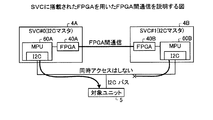
図2Aは、実施例に係る異常ユニット判定を実行するためのユニット間のI2Cバスの接続について説明する図である。図2Aに示すように、I2Cマスタユニット1A、1BとI2Cスレーブユニット3とは、同一のI2Cバスを用いて1対1で接続する。
FIG. 2A is a diagram illustrating connection of the I2C bus between units for executing abnormal unit determination according to the embodiment. As shown in FIG. 2A, the
また、I2Cマスタユニット1A、1BからI2Cスレーブユニット3へのI2Cバスの経路は、冗長化されている。すなわち、マスタユニット1Aは、自己に搭載されたI2Cマルチプレクサを介して、I2Cスレーブユニット3とI2Cバスで接続する。また、I2Cマスタユニット1Bは、自己に搭載されたI2Cマルチプレクサを介して、I2Cマスタユニット1Aと異なる経路でI2Cスレーブユニット3と接続する。そして、I2Cマスタユニット1AがI2Cマルチプレクサを介して、I2Cスレーブユニット3と接続しているとき、他方のI2Cマスタユニット1BはI2Cマルチプレクサにより未接続状態にし、I2Cスレーブユニット3と接続しないようにする。また、I2Cマスタユニット1BがI2Cマルチプレクサを介して、I2Cスレーブユニット3と接続しているとき、他方のI2Cマスタユニット1AはI2Cマルチプレクサにより未接続状態にし、I2Cスレーブユニット3と接続しないようにする。
Further, the path of the I2C bus from the
かかるユニット間の接続の下、I2Cマスタユニット1Aは、I2Cマスタユニット1Bと協調して、I2Cスレーブユニット3へそれぞれアクセスした結果である2個のアクセス結果を統合し、異常のI2Cユニットを判定する。
Under such a connection between the units, the
図2Bは、実施例に係る異常ユニットの判定方法を説明する図である。図2Bに示すように、横軸は一方のI2Cマスタユニットの異常判定情報J0を示し、縦軸は他方のI2Cマスタユニットの異常判定情報J1を示す。異常判定情報J0、J1は、異常となる可能性のあるアクセス箇所j1および当該箇所での異常内容j2を含む。符号J2で表されるマトリクスは、それぞれ2個のI2Cマスタユニットの異常判定情報から推定される異常ユニット群を示す。そして、I2Cマスタユニット1は、I2Cマスタユニット1のアクセス結果(異常発生箇所)とI2Cマスタユニット2のアクセス結果(異常発生箇所)とをマトリクスJ2上で交差(統合)して、異常のI2Cユニットを判定する。
FIG. 2B is a diagram illustrating a method for determining an abnormal unit according to the embodiment. As shown in FIG. 2B, the horizontal axis indicates abnormality determination information J0 of one I2C master unit, and the vertical axis indicates abnormality determination information J1 of the other I2C master unit. The abnormality determination information J0 and J1 includes an access location j1 that may be abnormal and an abnormal content j2 at the location. The matrix represented by the symbol J2 indicates an abnormal unit group estimated from the abnormality determination information of two I2C master units. Then, the
[実施例に係るI2Cバス装置の構成]
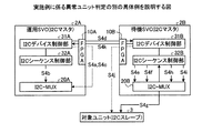
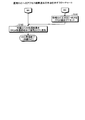
次に、図1は、本実施例に係るI2Cバス装置の構成を示す機能ブロック図である。図1に示すように、I2Cバス装置9は、I2Cマスタユニット1Aと、I2Cマスタユニット1Bと、I2Cスレーブユニット3とを備える。I2Cバス装置9は、例えば、複数のハードディスクを有するストレージデバイス格納筐体(DE)およびハードディスク以外のユニットが搭載された筐体(CE)を備えるストレージ装置である。I2Cマスタユニット1Aは、サービスコントローラ(SVC:Service Controller)といい、I2Cバスで接続する複数のI2Cスレーブユニット3を制御したり、監視したりする。I2Cマスタユニット1Aは、I2Cマスタユニット1Bと冗長構成であり、運用系となったり、待機系となったりする。以降の説明では、I2Cマスタユニット1Aが、運用系であるものとして説明する。そして、I2Cマスタユニット1Bは、I2Cマスタユニット1Aと同様の構成であるので、その説明を省略する。
[Configuration of I2C Bus Device According to Embodiment]
Next, FIG. 1 is a functional block diagram showing the configuration of the I2C bus device according to the present embodiment. As shown in FIG. 1, the
I2Cスレーブユニット3は、I2Cスレーブとなるユニットであり、I2Cマスタユニット1AおよびI2Cマスタユニット1Bとそれぞれ接続される。I2Cスレーブユニット3には、例えば、FRT(Frontend Router)、BRT(Backend Router)、PSU(Power Supply Unit)、BBU(Battery Backup Unit)が挙げられる。ここで、FRTは、ユニットの動作を管理するCM(Control Module)間の通信手段を提供するユニットである。BRTは、CMにハードディスクへのアクセス手段を提供するユニットである。PSUは、全ユニットに電力を供給するユニットである。BBUは、停電発生時に特定のユニットに電力を供給するユニットである。なお、図1では、説明の便宜上、I2Cスレーブユニット3が1台となる構成を採用しているが、I2Cスレーブユニット3が複数となる構成を適用しても良い。
The
I2Cマスタユニット1Aは、I2Cマスタとなるユニットであり、FPGA(Field Programmable Gate Array)10と、I2C−MUX(multiplexer)20と、制御部30と、記憶部40とを備える。FPGA10は、I2Cマスタユニット1Bと接続し、I2Cマスタユニット1BのFPGA間で通信する。また、FPGA10は、I2C−MUX20を初期化する際にリセットしたり、I2Cスレーブユニット3を初期化する際にリセットしたりする。
The
I2C−MUX20は、I2Cスレーブユニット3が複数ある場合、複数あるI2Cスレーブユニット3の内の1個のI2Cスレーブユニット3とI2Cバスで接続するようにし、接続したI2Cスレーブユニット3にアクセスする。かかるI2C−MUX20とI2Cスレーブユニット3とのI2Cバスの接続については、後述するものとする。
When there are a plurality of
制御部30は、I2Cデバイス制御部31およびI2Cシーケンス制御部32を有する。なお、制御部30は、例えば、ASIC(Application Specific Integrated Circuit)やFPGA(Field Programmable Gate Array)等の集積回路またはCPU(Central Processing Unit)やMPU(Micro Processing Unit)等の電子回路である。
The
記憶部40は、異常ユニット判定マトリクス41を有する。記憶部40は、例えば、RAM(Random Access Memory)、フラッシュメモリ(flash memory)等の半導体メモリ素子、または、ハードディスク、光ディスク等の記憶装置である。異常ユニット判定マトリクス41は、I2Cマスタユニットで異常となる可能性のある異常箇所に関するアクセス情報について、二重化されたI2Cマスタユニットのそれぞれのアクセス情報の組み合わせにより異常と判定されるユニットの候補を記憶する。かかる異常ユニット判定マトリクス41の構成については、後述するものとする。
The
I2Cデバイス制御部31は、I2Cスレーブユニット3およびI2Cマスタユニット1Bのデバイスを制御する。さらに、I2Cデバイス制御部31は、異常箇所判定部31aと、アクセス依頼部31bと、異常ユニット判定部31cとを有する。
The I2C
異常箇所判定部31aは、自ユニットと接続されたI2Cスレーブユニット3へのアクセスで異常箇所があるか否かを判定する。一例として、異常箇所判定部31aは、二重化された他系のI2Cマスタユニット1Bとの間のFPGA間通信を用いて、運用系となるか待機系となるかを調停したうえで決定する。
The abnormal
また、異常箇所判定部31aは、運用系と決定された場合に、アクセス対象となるI2Cスレーブユニット3(以降、「対象ユニット」という。)との接続または切断を、I2Cシーケンス制御部32を介してI2C―MUX20を制御して行う。
In addition, when the abnormal
また、異常箇所判定部31aは、対象ユニットへのアクセスで異常となる異常箇所があった場合、異常箇所に基づいてI2C−MUX20または対象ユニットのI2CデバイスをFPGA10経由でリセットする。ここで、対象ユニットへのアクセスでの異常には、「I2Cシーケンス異常」と、「I2Cデバイス異常」とがある。「I2Cシーケンス異常」とは、後述するI2Cシーケンス制御部32によって異常を検出した場合を示す。例えば、バスの使用権を獲得するために使用する制御信号を示すスタートコンディションまたはバスを解放するために使用する制御信号を示すストップコンディションの検出ができなかった場合、対象ユニットから正常終了であることを通知するACKを検出できなかった場合やオーバランエラーを検出した場合等がある。また、I2Cデバイス異常とは、異常箇所判定部31aによって異常を検出した場合を示す。例えば、対象ユニットのI2Cデバイスが期待した動作をしない場合がある。
In addition, when there is an abnormal part that becomes abnormal when accessing the target unit, the abnormal
また、異常箇所判定部31aは、対象ユニットのI2Cデバイスを指定し、指定したI2Cデバイスのレジスタの読み込み、および指定したI2Cデバイスのレジスタへの書き込みを、I2Cシーケンス制御部3を介してする。なお、異常箇所判定部31aは、指定したI2Cデバイスのレジスタの読み込み、および指定したI2Cデバイスのレジスタへの書き込みのどちらか一方を、I2Cシーケンス制御部3を介してするようにしても良い。
The abnormal
また、異常箇所判定部31aは、待機系と決定された場合に、運用系のI2Cマスタユニット1AからFPGA間通信を介した、対象ユニットへのアクセス依頼を待ち受ける。そして、異常箇所判定部31aは、対象ユニットへのアクセス依頼を受け取ると、当該対象ユニットへのアクセスを実行し、アクセス結果を、FPGA間通信を介して運用系のI2Cマスタユニット1Aに通知する。
In addition, when it is determined as the standby system, the abnormal
アクセス依頼部31bは、異常箇所判定部31aによって対象ユニットへのアクセスで異常箇所があると判定された場合に、対象ユニットと同一の対象ユニットへのアクセスを、待機系側のI2Cマスタユニット1Bに依頼する。
The
異常ユニット判定部31cは、異常箇所判定部31aによって判定された異常箇所に関するアクセス結果とアクセス依頼部31bによる依頼結果を示すアクセス結果との組み合わせを用いて、異常であるユニットを判定する。一例として、異常ユニット判定部31cは、異常ユニット判定マトリクス41に記憶された、I2Cマスタユニットのそれぞれの異常判定情報の組み合わせと、実際に実行されたそれぞれのアクセス結果の組み合わせとを用いて、異常のユニットを判定する。異常判定情報は、異常となる可能性のある箇所および当該箇所での異常内容を含むものである。例えば、異常判定情報には、I2C−MUXとアクセスした際のシーケンス異常およびデバイス異常がある。また、異常判定情報には、対象ユニットと接続した際のシーケンス異常、対象ユニットと接続後に読み書きした際のシーケンス異常およびデバイス異常等がある。かかる異常判定情報の詳細は、後述するものとする。
The abnormal unit determination unit 31c determines a unit that is abnormal using a combination of an access result related to the abnormal location determined by the abnormal
I2Cシーケンス制御部32は、I2Cのシーケンスに用いられる各種信号や各種コマンドを対象ユニットに送信したり、検出したりする。一例として、I2Cシーケンス制御部32は、スタートコンディションの制御信号またはストップコンディションの制御信号を対象ユニットに送出したり、検出したりする。また、I2Cシーケンス制御部32は、ACKを対象ユニットに送出したり、検出したりする。また、I2Cシーケンス制御部32は、異常箇所判定部31aから指定された対象ユニットのデバイスに対するアドレスデータ、レジスタデータまたは書き込みデータを該当コマンドとともにI2Cバス上に送信する。そして、I2Cシーケンス制御部32は、対象ユニットから該当コマンドに対応するレジスタデータを受信し、異常箇所判定部31aに通知する。
The I2C
また、I2Cシーケンス制御部32は、I2Cのシーケンスの異常を、「I2Cシーケンス異常」として検出する。
Further, the I2C
[異常箇所判定についての説明]
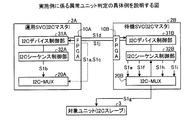
ここで、異常判定部31aによる異常箇所判定について、図3を参照しながら説明する。図3は、実施例に係る異常箇所判定を説明する図である。なお、図3では、運用SVC2Aが運用系のI2Cマスタユニットに相当し、待機SVC2Bが待機系のI2Cマスタユニットに相当するものとする。図3に示すように、運用SVC2Aは、待機SVC2Bと二重化され、自己に搭載されたI2C−MUX20Aを介して、対象ユニット3とI2Cバスで接続する。なお、説明内の「 」内の符号は、各異常種別を表すものとする。
[Explanation of abnormal location determination]
Here, the abnormality location determination by the
運用SVC2AのI2Cデバイス制御部31Aは、FPGA10Aと待機SVC2BのFPGA10Bとを介して、自己が運用系となるか待機系となるかを調停し決定する(S1)。ここでは、I2Cデバイス制御部31Aは、運用SVC2Aが運用系となると決定したものとする。
The I2C
次に、運用系と決定した運用SVC2Aは、I2Cシーケンス制御部32Aを介して、I2C−MUX20Aのステータスを、例えばI2C−MUX20Aの記憶部から読み出して確認する(S2)。ここで、I2Cシーケンス制御部32Aが、I2C−MUX20Aへのアクセスで異常を検出した場合、I2Cデバイス制御部31Aは、I2Cシーケンス異常「e1」と判定する。また、I2Cデバイス制御部31Aが、I2C−MUX20Aのステータスが期待した状態でないような異常を検出した場合、I2Cデバイス制御部31Aは、デバイス異常「e2」と判定する。なお、I2C−MUX20Aのステータスが期待した状態でないような異常とは、例えば、対象ユニットと既に接続状態となっているような場合がある。そして、I2Cデバイス制御部31Aは、I2C−MUX20Aのステータスの異常を検出した場合、I2C−MUX20Aをリセットによる切断をしたうえで、待機系と決定した待機SVC2Bに対し、対象ユニット3へのアクセス依頼を行い、アクセス結果を待ち受けることとなる。
Next, the operating
次に、運用SVC2Aは、I2Cシーケンス制御部32Aを介して、I2C−MUX20Aを対象ユニット3と接続する(S3)。ここで、I2Cデバイス制御部31Aが、I2C−MUX20Aへのアクセスで異常を検出した場合、I2Cデバイス制御部31Aは、I2Cシーケンス異常「e3」と判定する。そして、I2Cデバイス制御部31Aは、対象ユニット3との接続異常を検出した場合、I2C−MUX20Aをリセットによる切断をしたうえで、待機系と決定した待機SVC2Bに対し、対象ユニット3へのアクセス依頼を行い、アクセス結果を待ち受けることとなる。
Next, the
続いて、運用SVC2Aは、I2Cシーケンス制御部32Aを介して、I2C−MUX20Aのレジスタの値が例えば所定値に更新されることを確認することで、I2C−MUX20Aが対象ユニット3と接続したことを確認する(S4)。ここで、I2Cシーケンス制御部32Aが、I2C−MUX20Aへのアクセスで異常を検出した場合、I2Cデバイス制御部31Aは、I2Cシーケンス異常「e4」と判定する。また、I2Cデバイス制御部31Aが、I2C−MUX20Aのレジスタが期待した状態でない異常を検出した場合、I2Cデバイス制御部31Aは、I2Cデバイス異常「e5」と判定する。なお、I2C−MUX20Aのレジスタが期待した状態でない異常とは、例えば、I2C−MUX20Aが対象ユニット3とのみ接続されていない場合がある。そして、I2Cデバイス制御部31Aは、対象ユニット3との接続異常を検出した場合、I2C−MUX20Aをリセットによる切断をしたうえで、待機系と決定した待機SVC2Bに対し、対象ユニット3へのアクセス依頼を行い、アクセス結果を待ち受けることとなる。
Subsequently, the
続いて、運用SVC2Aは、I2Cシーケンス制御部32Aを介して、対象ユニット3から目的のデータを読み取り、または対象ユニット3に目的のデータを書き込む(S5)。ここで、I2Cシーケンス制御部32Aが、対象ユニット3へのアクセスで異常を検出した場合、I2Cデバイス制御部31Aは、I2Cシーケンス異常「e6」と判定する。また、I2Cデバイス制御部31Aが、期待した値でない異常を検出した場合、I2Cデバイス制御部31Aは、I2Cデバイス異常「e7」と判定する。なお、期待した値でない異常とは、例えば、対象ユニット3のデバイスからの読み取り値がデバイス上あり得ない値であったり、対象ユニット3のデバイスの指定した位置に正しい値が書き込めなかったりした場合がある。そして、I2Cデバイス制御部31Aは、対象ユニット3とのアクセス異常を検出した場合、I2C−MUX20Aをリセットによる切断をしたうえで、待機系と決定した待機SVC2Bに対し、対象ユニット3へのアクセス依頼を行い、アクセス結果を待ち受けることとなる。
Subsequently, the
さらに、運用SVC2Aは、I2Cシーケンス制御部32Aを介して、I2C−MUX20Aを対象ユニット3から切断する(S6)。ここで、I2Cデバイス制御部31Aが、I2C−MUX20Aへのアクセスで異常を検出した場合、I2Cデバイス制御部31Aは、I2Cシーケンス異常「e8」と判定する。そして、I2Cデバイス制御部31Aは、対象ユニット3との切断異常を検出した場合、I2C−MUX20Aをリセットによる切断をしたうえで、待機系と決定した待機SVC2Bに対し、対象ユニット3へのアクセス依頼を行い、アクセス結果を待ち受けることとなる。
Further, the
続いて、運用SVC2Aは、I2Cシーケンス制御部32Aを介して、I2C−MUX20Aのレジスタで、I2C−MUX20Aを対象ユニット3から切断したことを確認する(S7)。ここで、I2Cシーケンス制御部32Aが、I2C−MUX20Aへのアクセスで異常を検出した場合、I2Cデバイス制御部31Aは、I2Cシーケンス異常「e9」と判定する。また、I2Cデバイス制御部31Aが、I2C−MUX20Aのレジスタが期待した状態でない異常を検出した場合、I2Cデバイス制御部31Aは、I2Cデバイス異常「e10」と判定する。なお、I2C−MUX20Aのレジスタが期待した状態でない異常とは、例えば、I2C−MUX20Aが対象ユニット3と未接続状態とならなかったような場合がある。
Subsequently, the
[異常ユニット判定マトリクスの一例]
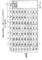
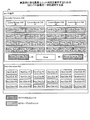
次に、異常ユニット判定マトリクス41の一例について、図4を参照しながら説明する。図4は、異常ユニット判定マトリクス41の一例を示す図である。図4に示すように、異常ユニット判定マトリクス41は、横軸に運用SVCの異常判定情報41A、縦軸に待機SVCの異常判定情報41Bを記憶する。運用SVCの異常判定情報41Aには、異常となる可能性のある箇所と異常内容とからなる異常種別(正常を含む)を複数記憶する。待機SVCの異常判定情報41Bには、運用SVCの異常判定情報41Aと同様に異常種別を複数記憶する。
[Example of abnormal unit determination matrix]
Next, an example of the abnormal
以下に、異常種別の例を示す。例えば、符号411で示す運用SVCの異常種別が「e1」の場合には、運用SVCがI2C−MUX20Aのステータスを確認する箇所で、I2Cシーケンス異常となる場合である。符号412で示す運用SVCの異常種別が「e2」の場合には、運用SVCがI2C−MUX20Aのステータスを確認する箇所で、I2Cデバイス異常となる場合である。符号413で示す運用SVCの異常種別が「e3」の場合には、運用SVCがI2C−MUX20Aを対象ユニット3と接続する箇所で、I2Cシーケンス異常となる場合である。符号414で示す運用SVCの異常種別が「e4」の場合には、運用SVCがI2C−MUX20Aのレジスタで、I2C−MUX20Aが対象ユニットと接続したことを確認する箇所で、I2Cシーケンス異常となる場合である。符号415で示す運用SVCの異常種別が「e5」の場合には、運用SVCがI2C−MUX20Aのレジスタで、I2C−MUX20Aが対象ユニットと接続したことを確認する箇所で、I2Cデバイス異常となる場合である。符号416で示す運用SVCの異常種別が「e6」の場合には、運用SVCが対象ユニット3とアクセスする箇所で、I2Cシーケンス異常となる場合である。符号417で示す運用SVCの異常種別が「e7」の場合には、運用SVCが対象ユニット3とアクセスする箇所で、I2Cデバイス異常となる場合である。符号418で示す運用SVCの異常種別が「e8」の場合には、運用SVCがI2C-MUXから対象ユニットを切断する箇所で、I2Cシーケンス異常となる場合である。運用SVCの異常種別が「e9」の場合には、運用SVCがI2C−MUX20Aのレジスタで、I2C−MUX20Aを対象ユニットから切断したことを確認する箇所で、I2Cシーケンス異常となる場合である。運用SVCの異常種別が「e10」の場合には、運用SVCがI2C−MUX20Aのレジスタで、I2C−MUX20Aを対象ユニットから切断したことを確認する箇所で、I2Cデバイス異常となる場合である。なお、待機系SVCの異常判定情報41Aの異常種別は、運用SVCの異常判定情報41Bの異常種別と同様であるので、説明を省略する。
An example of the abnormality type is shown below. For example, when the operation SVC abnormality type indicated by
異常ユニット情報41Cは、運用系SVCの異常判定情報41Aの異常種別と待機系SVCの異常判定情報41Bの異常種別との組み合わせにより異常を判別できるユニットの候補を記憶する。図4の例では、符号eu1では、運用SVCの異常種別「e1」と待機SVCの異常種別「正常」との組み合わせにより判別できる、異常となるユニットの候補を「運用SVC」として記憶する。
The
[異常ユニット判定の具体例]
次に、運用SVC2Aから対象ユニット3へのアクセスで異常となる異常箇所があった場合に、異常箇所に基づいて異常ユニットを判定する具体例を、図5〜図8を参照しながら説明する。
[Specific example of abnormal unit judgment]
Next, a specific example of determining an abnormal unit based on the abnormal location when there is an abnormal location that becomes abnormal when accessing the
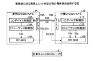
図5は、実施例に係る異常ユニット判定の具体例を説明する図である。なお、図5では、運用SVC2AがI2C−MUX20Aのステータスを確認する箇所で、I2Cシーケンス異常(「e1」)となった場合を説明する。そこで、I2Cデバイス制御部31Aが、最初にI2Cシーケンス異常「e1」と判定した後の動作について説明する。
FIG. 5 is a diagram illustrating a specific example of the abnormal unit determination according to the embodiment. Note that FIG. 5 illustrates a case where the
最初にI2Cシーケンス異常「e1」と判定したI2Cデバイス制御部31Aは、FPGA経由で、I2C−MUX20Aをリセットする(S1a)。その後、I2Cデバイス制御部31Aは、I2C−MUX20Aのステータスの確認を再試行する(S1b)。そして、I2Cデバイス制御部31Aは、再試行してもI2Cシーケンス異常が回復しない場合、再試行回数がX回に達したとき、運用SVC2Aからの接続を断念する。ここでは、I2Cデバイス制御部31Aは、自己のアクセス結果を「e1」として記憶部40に保持する。
The I2C
そして、I2Cデバイス制御部31Aは、待機系での動作に影響を与えないように、FPGA経由で、I2C−MUX20Aを再度リセットする(S1c)。そして、I2Cデバイス制御部31Aは、待機SVC2Bに対し、FPGA間通信を用いて、対象ユニット3への接続確認を依頼する(S1d)。すなわち、I2Cデバイス制御部31Aは、対象ユニット3へのアクセス依頼を行う。
Then, the I2C
続いて、対象ユニット3への接続確認を依頼された待機SVC2BのI2Cデバイス制御部31Bは、I2C−MUX20Bのステータスを確認した後、I2C−MUX20Bを対象ユニット3と接続する(S1e)。そして、I2Cデバイス制御部31Bは、I2C-MUX20Bのレジスタで、I2C−MUX20Bが対象ユニット3と接続したことを確認する(S1f)。さらに、I2Cデバイス制御部31Bは、対象ユニット3から目的のデータを読み取り、または対象ユニット3に目的のデータを書き込む(S1g)。
Subsequently, the I2C
続いて、I2Cデバイス制御部31Bは、I2C−MUX20Bを対象ユニット3から切断する(S1h)。そして、I2Cデバイス制御部31Bは、I2C−MUX20Bのレジスタで、I2C−MUX20Bを対象ユニット3から切断したことを確認する(S1i)。そして、I2Cデバイス制御部31Bは、運用SVC2Aに対し、FPGA間通信を用いて、対象ユニット3とのアクセス結果を通知する(S1j)。ここでは、I2Cデバイス制御部31Bは、自己のアクセス結果を「正常」として通知する。
Subsequently, the I2C
運用SVC2AのI2Cデバイス制御部31Aは、待機SVC2Bから対象ユニット3とのアクセス結果を受け取る。そして、I2Cデバイス制御部31Aは、異常ユニット判定マトリクス41に基づいて、運用SVC2Aのアクセス結果および待機SVC2Bのアクセス結果から異常ユニットを判定する。ここでは、I2Cデバイス制御部31Aは、運用SVC1Aのアクセス結果が「e1」であり、待機SVC2Aのアクセス結果が「正常」であるので、異常ユニット判定マトリクス41(図4参照)に基づいて、異常ユニットを「運用SVC」として判定する。
The I2C
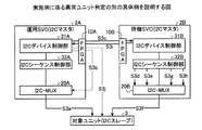
図6は、実施例に係る異常ユニット判定の別の具体例を説明する図である。なお、図6では、運用SVC2Aおよび待機SVC2Bが各I2C−MUX20のステータスを確認する箇所で、I2Cシーケンス異常(「e1」)となる場合を説明する。そこで、運用SVC2AのI2Cデバイス制御部31Aが、最初にI2Cシーケンス異常「e1」と判定した後の動作について説明する。
FIG. 6 is a diagram illustrating another specific example of the abnormal unit determination according to the embodiment. FIG. 6 illustrates a case where an I2C sequence error (“e1”) occurs at a location where the
最初にI2Cシーケンス異常「e1」と判定したI2Cデバイス制御部31Aは、FPGA経由で、I2C−MUX20Aをリセットする(S2a)。その後、I2Cデバイス制御部31Aは、I2C−MUX20Aのステータスの確認を再試行する(S2b)。そして、I2Cデバイス制御部31Aは、再試行しても回復しない場合、再試行回数がX回に達したとき、運用SVC1Aからの接続を断念する。ここでは、I2Cデバイス制御部31Aは、自己のアクセス結果を「e1」として記憶部40に保持する。
The I2C
そして、I2Cデバイス制御部31Aは、待機系での動作に影響を与えないように、FPGA経由で、I2C−MUX20Aを再度リセットする(S2c)。そして、I2Cデバイス制御部31Aは、待機SVC2Bに対し、FPGA間通信を用いて、対象ユニット3への接続確認を依頼する(S2d)。すなわち、I2Cデバイス制御部31Aは、対象ユニット3へのアクセス依頼を行う。
Then, the I2C
続いて、対象ユニット3への接続確認を依頼された待機SVC2BのI2Cデバイス制御部31Bは、I2C−MUX20Bのステータスを確認する(S2e)。ところが、I2Cデバイス制御部31Bは、I2C−MUX20Bへのアクセスで異常を検出したので、I2Cシーケンス異常「e1」と判定する。そこで、I2Cデバイス制御部31Bは、FPGA経由で、I2C−MUX20Bをリセットする(S2f)。その後、I2Cデバイス制御部31Bは、I2C−MUX20Bのステータスの確認を再試行する(S2g)。そして、I2Cデバイス制御部31Bは、再試行しても回復しない場合、再試行回数がX回に達したとき、待機SVC2Bからの接続を断念する。ここでは、I2Cデバイス制御部31Bは、自己のアクセス結果を「e1」として待機系SVCの記憶部40に保持する。
Subsequently, the I2C
そして、I2Cデバイス制御部31Bは、運用系での動作に影響を与えないように、FPGA経由で、I2C−MUX20Bを再度リセットする(S2h)。そして、I2Cデバイス制御部31Bは、運用SVC2Aに対し、FPGA間通信を用いて、対象ユニット3とのアクセス結果を通知する(S2i)。ここでは、I2Cデバイス制御部31Bは、自己のアクセス結果を「e1」として通知する。
Then, the I2C
運用SVC2AのI2Cデバイス制御部31Aは、待機SVC2Bから対象ユニット3とのアクセス結果を受け取る。そして、I2Cデバイス制御部31Aは、異常ユニット判定マトリクス41に基づいて、運用SVC2Aのアクセス結果および待機SVC2Bのアクセス結果から異常ユニットを判定する。ここでは、I2Cデバイス制御部31Aは、運用SVC2Aのアクセス結果が「e1」であり、待機SVC2Bのアクセス結果が「e1」であるので、異常ユニット判定マトリクス41に基づいて、異常ユニットを「運用SVC、待機SVC」として判定する。つまり、アクセス結果が「e1」である場合は、I2C−MUX20へのアクセスそのもので異常を検出した場合であり、対象ユニット3までアクセスされていないので、異常ユニットを「運用SVC、待機SVC」とする。
The I2C
図7は、実施例に係る異常ユニット判定の別の具体例を説明する図である。なお、図7では、運用SVC2Aおよび待機SVC2Bが対象ユニット3から目的のデータを読み取る箇所で、I2Cデバイス異常(「e7」)となる場合を説明する。そこで、I2Cデバイス制御部31Aが、最初にI2Cデバイス異常「e7」と判定した後の動作について説明する。
FIG. 7 is a diagram illustrating another specific example of the abnormal unit determination according to the embodiment. FIG. 7 illustrates a case where the
最初にI2Cデバイス異常「e7」と判定したI2Cデバイス制御部31Aは、対象ユニット3から目的のデータを読み取る動作を再試行する(S3a)。そして、I2Cデバイス制御部31Aは、再試行しても回復しない場合、再試行回数がX回に達したとき、運用SVC2Aからの接続を断念し、FPGA経由で、I2C−MUX20Aをリセットする(S3b)。これにより、I2Cデバイス制御部31Aは、対象ユニット3との接続を強制的に切断する。そして、I2Cデバイス制御部31Aは、自己のアクセス結果を「e7」として記憶部40に保持する。そして、I2Cデバイス制御部31Aは、待機SVC2Bに対し、FPGA間通信を用いて、対象ユニット3への接続確認を依頼する(S3c)。すなわち、I2Cデバイス制御部31Aは、対象ユニット3へのアクセス依頼を行う。
The I2C
続いて、対象ユニット3への接続確認を依頼された待機SVC2BのI2Cデバイス制御部31Bは、I2C−MUX20Bを対象ユニット3と接続する(S3d)。続いて、I2Cデバイス制御部31Bは、I2C-MUX20Bのレジスタで、I2C−MUX20Bが対象ユニット3と接続したことを確認する(S3e)。
Subsequently, the I2C
続いて、I2Cデバイス制御部31Bは、対象ユニット3から目的のデータを読み取る(S3f)。ところが、I2Cデバイス制御部31Bは、期待した値を読み取れなかったので、I2Cデバイス異常「e7」と判定する。その後、I2Cデバイス制御部31Bは、対象ユニット3から目的のデータの読み取りを再試行し、再試行しても回復しない場合、再試行回数がX回に達したとき、待機SVC2Bからの接続を断念する。
Subsequently, the I2C
そして、I2Cデバイス制御部31Bは、I2C−MUX20BをFPGA経由でリセットしたうえで、I2C−MUX20Bを対象ユニット3から切断する(S3g)。さらに、I2Cデバイス制御部31Bは、I2C-MUX20BのレジスタでI2C−MUX20Bを対象ユニット3から切断したことを確認する(S3h)。
Then, the I2C
そして、I2Cデバイス制御部31Bは、運用SVC2Aに対し、FPGA間通信を用いて、対象ユニット3とのアクセス結果を通知する(S3i)。ここでは、I2Cデバイス制御部31Bは、自己のアクセス結果を「e7」として通知する。
Then, the I2C
運用SVC2AのI2Cデバイス制御部31Aは、待機SVC2Bから対象ユニット3とのアクセス結果を受け取る。そして、I2Cデバイス制御部31Aは、異常ユニット判定マトリクス41に基づいて、運用SVC2Aのアクセス結果および待機SVC2Bのアクセス結果から異常ユニットを判定する。ここでは、I2Cデバイス制御部31Aは、運用SVC2Aのアクセス結果が「e7」であり、待機SVC2Bのアクセス結果が「e7」であるので、異常ユニット判定マトリクス41に基づいて、異常ユニットを「対象ユニット」として判定する。この場合には、I2Cデバイス制御部31Aは、FPGAで対象ユニット3をリセットする(S3j)。そして、I2Cデバイス制御部31Aは、I2C−MUX20Aが切断されているので、I2C−MUX20Aの状態を確認し、I2C−MUX20Aと接続したうえでS3aから再実施する。そして、I2Cデバイス制御部31Aは、再実施後も異常ユニットを「対象ユニット」として判定する場合には、異常ユニットを「対象ユニット」として確定する。
The I2C
なお、S3fにおいて、I2Cデバイス制御部31Bが、対象ユニット3から目的のデータを読み取る再試行で期待した値を読み取れた場合には、運用SVC2Aに対し、待機SVC2Bのアクセス結果を「正常」として通知する。この場合には、I2Cデバイス制御部31Aは、異常ユニットを「運用SVC」として判定することとなる。
In S3f, when the I2C
図8は、実施例に係る異常ユニット判定の別の具体例を説明する図である。なお、図8では、運用SVC2AがI2C−MUX20Aのステータスを確認する箇所で、I2Cシーケンス異常(「e1」)となり、待機SVC2Bが対象ユニット3とアクセスする箇所で、I2Cデバイス異常(「e7」)となる場合を説明する。そこで、運用SVC2AのI2Cデバイス制御部31Aが、最初にI2Cシーケンス異常「e1」と判定した後の動作について説明する。
FIG. 8 is a diagram for explaining another specific example of the abnormal unit determination according to the embodiment. In FIG. 8, an I2C sequence error (“e1”) occurs at the location where the
最初にI2Cシーケンス異常「e1」と判定したI2Cデバイス制御部31Aは、FPGA経由で、I2C−MUX20Aをリセットする(S4a)。その後、I2Cデバイス制御部31Aは、I2C−MUX20Aのステータスの確認を再試行する(S4b)。そして、I2Cデバイス制御部31Aは、再試行しても回復しない場合、再試行回数がX回に達したとき、運用SVC2Aからの接続を断念する。ここでは、I2Cデバイス制御部31Aは、自己のアクセス結果を「e1」として記憶部40に保持する。
The I2C
そして、I2Cデバイス制御部31Aは、待機系での動作に影響を与えないように、FPGA経由で、I2C−MUX20Aを再度リセットする(S4c)。そして、I2Cデバイス制御部31Aは、待機SVC2Bに対し、FPGA間通信を用いて、対象ユニット3への接続確認を依頼する(S4d)。すなわち、I2Cデバイス制御部31Aは、対象ユニット3へのアクセス依頼を行う。
Then, the I2C
続いて、対象ユニット3への接続確認を依頼された待機SVC2BのI2Cデバイス制御部31Bは、I2C−MUX20Bを対象ユニット3と接続する(S4e)。続いて、I2Cデバイス制御部31Bは、I2C-MUX20Bのレジスタで、I2C−MUX20Bが対象ユニット3と接続したことを確認する(S4f)。
Subsequently, the I2C
続いて、I2Cデバイス制御部31Bは、対象ユニット3から目的のデータを読み取る(S4g)。ところが、I2Cデバイス制御部31Bは、期待した値を読み取れなかったので、I2Cデバイス異常「e7」と判定する。その後、I2Cデバイス制御部31Bは、対象ユニット3から目的のデータの読み取りを再試行し、再試行しても回復しない場合、再試行回数がX回に達したとき、待機SVC2Bからの接続を断念する。
Subsequently, the I2C
そして、I2Cデバイス制御部31Bは、FPGA経由でI2C−MUX20Bをリセットしたうえで、I2C−MUX20Bを対象ユニット3から切断する(S4h)。さらに、I2Cデバイス制御部31Bは、I2C-MUX20BのレジスタでI2C−MUX20Bを対象ユニット3から切断したことを確認する(S4i)。なお、I2Cデバイス制御部31Bは、運用SVC2Aから接続確認の依頼を受けたとき、運用SVC2Aの異常が判明している場合、FPGA10B経由で対象ユニット3をリセットし(S4j)、対象ユニット3と接続する処理(S4e)から再試行しても良い。
Then, the I2C
そして、I2Cデバイス制御部31Bは、運用SVC2Aに対し、FPGA間通信を用いて、対象ユニット3とのアクセス結果を通知する(S4k)。ここでは、I2Cデバイス制御部31Bは、自己のアクセス結果を「e7」として通知する。
The I2C
運用SVC2AのI2Cデバイス制御部31Aは、待機SVC2Bから対象ユニット3とのアクセス結果を受け取る。そして、I2Cデバイス制御部31Aは、異常ユニット判定マトリクス41に基づいて、運用SVC2Aのアクセス結果および待機SVC2Bのアクセス結果から異常ユニットを判定する。ここでは、I2Cデバイス制御部31Aは、運用SVC2Aのアクセス結果が「e1」であり、待機SVC2Bのアクセス結果が「e7」であるので、異常ユニット判定マトリクス41に基づいて、異常ユニットを「運用SVC、対象ユニット」として判定する。
The I2C
なお、S4jの処理後、I2Cデバイス制御部31Bが、対象ユニット3から目的のデータを読み取る再試行で期待した値を読み取れた場合には、運用SVC2Aに対し、待機SVC2Bのアクセス結果を「正常」として通知する。この場合には、I2Cデバイス制御部31Aは、異常ユニットを「運用SVC」として判定することとなる。
After the process of S4j, if the I2C
[異常ユニット判定を実行するためのI2Cバス装置]
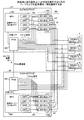
次に、実施例に係る異常ユニット判定を実行するためのI2Cバス装置について、図9を参照しながら説明する。図9は、実施例に係る異常ユニット判定を実行するためのI2Cバス装置の一例を説明する図である。図9に示すように、I2Cバス装置9Aは、ハードディスクが搭載される筐体(DE:Device Enclosure)とハードディスク以外のユニットが搭載される筐体(CE:Controller Enclosure)を有する。DEには、複数のハードディスク(Hard Disk)が搭載されている。また、CEには、ユニットの動作を管理するユニット(CM:Control Module)、CM間の通信手段を提供するユニット(FRT:Frontend Router)、CMにハードディスクへのアクセス手段を提供するユニット(BRT:Backend Router)が搭載されている。また、CEには、CEに搭載される全ユニットに電力を供給するユニット(PSU:Power Supply Unit)、停電発生時に特定のユニットに電力を供給するユニット(BBU:Battery Backup Unit)が搭載されている。さらに、CEには、ユーザの操作により自装置に電源を投入したり切断したりするユニット(Panel)および自装置を制御したり監視したりするユニット(SVC:Service Controller)が搭載されている。なお、SVC4Aが図1のI2Cマスタユニット1Aに相当し、SVC4Bが図1のI2Cマスタユニット1Bに相当する。また、符号5で表したFRT、BRT、PSUおよびBBUが図1のI2Cスレーブユニット3(対象ユニット)に相当する。
[I2C bus device for executing abnormal unit determination]
Next, an I2C bus device for executing abnormal unit determination according to the embodiment will be described with reference to FIG. FIG. 9 is a diagram illustrating an example of the I2C bus device for executing the abnormal unit determination according to the embodiment. As shown in FIG. 9, the
[異常ユニット判定を実行するためのハードウェアの全体構成]
次に、実施例に係る異常ユニット判定を実行するためのハードウェアの全体構成について、図10を参照しながら説明する。図10は、実施例に係る異常ユニット判定を実行するためのハードウェアの全体構成の一例を説明する図である。図10に示すように、SVC4Aは、FPGA40A、I2C−MUX50AおよびMPU60Aを有する。SVC4Aは、SVC4Bと冗長構成となっている。また、SVC4Aは、SVC4Bと、それぞれに搭載されたFPGA40A、40Bを介して接続する。また、SVC4Aは、I2C−MUX50Aを介して、対象ユニット5とI2Cバスで接続する。
[Hardware configuration for executing abnormal unit determination]
Next, the overall hardware configuration for executing the abnormal unit determination according to the embodiment will be described with reference to FIG. FIG. 10 is a diagram illustrating an example of an overall hardware configuration for executing the abnormal unit determination according to the embodiment. As shown in FIG. 10, the
I2C−MUX50AのそれぞれのI2C−MUXm1〜m4は、I2Cバスを介して、それぞれの対象ユニットs1〜s4と1対1で接続する。さらに、I2C−MUX50BのそれぞれのI2C−MUXm1〜m4は、I2C−MUX50Aが介するI2Cバスと異なるI2Cバスを介してそれぞれの対象ユニットs1〜s4と1対1で接続する。一例として、I2C−MUX50AのI2C−MUXm1は、FRT#0〜3を有する対象ユニットs1と1対1で接続している。さらに、I2C−MUX50BのI2C−MUXm1は、同じ対象ユニットs1と、異なるI2Cバスを介して1対1で接続する。なお、FPGA40Aが図1のFPGA10に相当し、I2C−MUX50Aが図1のI2C−MUX20に相当する。また、MPU60Aが図1の制御部30に相当する。
Each I2C-MUX m1 to m4 of the I2C-
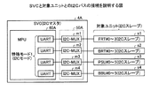
ここで、SVC4Aと対象ユニットs1〜s4とのI2Cバスの接続について、図11を参照して説明する。図11は、SVCと対象ユニットとのI2Cバスの接続を説明する図である。図11に示すように、SVC4Aは、MPU60Aの通信回路であるUART(Universal Asynchronous Receiver Transmitter)を特殊モード1(I2Cモード)でI2C−MUX50Aと接続する。そして、I2C−MUX50AのそれぞれのI2C−MUXm1〜m4は、それぞれの対象ユニットs1〜s4とI2CインタフェースをI2Cモードで接続する。
Here, the connection of the I2C bus between the
次に、異常ユニット判定を実行する際に用いられるFPGA間通信について、図12を参照しながら説明する。図12は、SVCに搭載されたFPGAを用いたFPGA間通信を説明する図である。図12に示すように、SVC4Aは、対象ユニット5へのアクセスの際、FPGA間通信を用いて、二重化されたSVC4Bとの間で調停し、運用系となるか待機系となるかを決定する。すなわち、両方のSVC4A、4Bが、同一の対象ユニット5に同時にアクセスしないようにするのである。また、SVC4Aは、アクセスする対象ユニット5単位、すなわち対象ユニット5と接続することとなるUART単位に、SVC4Bとの間でどちらが運用系となるか待機系となるかを決定する。なお、FPGA間通信を用いて運用系となるか待機系となるかを調停する処理は、前述した異常箇所判定部31aによって行われる。
Next, the inter-FPGA communication used when executing the abnormal unit determination will be described with reference to FIG. FIG. 12 is a diagram for explaining inter-FPGA communication using an FPGA mounted on the SVC. As shown in FIG. 12, when accessing the
次に、異常ユニット判定を実行する際に、異常箇所があった場合のリセット制御について、図13を参照しながら説明する。図13は、SVCに搭載されたFPGAを用いたリセット制御を説明する図である。図13に示すように、FPGA40Aは、それぞれの対象ユニットs1〜s4のI2Cデバイスを個別にリセットする。また、FPGA40Aは、I2C−MUX50のそれぞれのI2C−MUXm1〜m4を個別にリセットする。リセットされたI2C−MUXm1〜m4では、その後、すべての接続が切断される。なお、異常箇所があった場合のリセット制御の処理は、前述した異常箇所判定部31aによって行われる。例えば、異常箇所判定部31aは、対象ユニットs1のI2CデバイスであるFRT#0から目的のデータを読み取れないデバイス異常「e7」となった場合、FRT#0をFPGA40A経由でリセットする(g1)。また、異常箇所判定部31aは、I2C−MUXm1へのアクセスでI2Cシーケンス異常「e1」となった場合、I2C−MUXm1をFPGA40A経由でリセットする(g2)。
Next, reset control in the case where there is an abnormal part when executing the abnormal unit determination will be described with reference to FIG. FIG. 13 is a diagram for explaining the reset control using the FPGA mounted on the SVC. As illustrated in FIG. 13, the
ここで、SVC4A、4Bに搭載されたI2C−MUXの接続方法について、図14を参照して説明する。図14は、SVCに搭載されたI2C−MUXの接続方法について説明する図である。なお、図14では、SVC4Aに搭載された1個のI2C−MUXm1に着目して説明するものとする。図14に示すように、I2C−MUXm1は、MPU60AのUARTと入力端子m10で接続する。また、I2C−MUXm1は、複数の出力端子m11〜m14で対象ユニットs1のFRT#0(s11)〜#3(s14)と接続することで、1個の対象ユニットs1のみと接続する。これにより、SVC4Aに搭載されたMPU60Aは、I2C−MUXm1によって対象ユニットs1と1対1で接続することとなる。
Here, a method of connecting the I2C-MUX mounted on the
また、I2C−MUXm1は、FPGA40Aからのリセット信号でリセットされる。これにより、I2C−MUXm1では、すべての接続が切断される。例えば、図14では、I2C−MUXm1は、出力端子m14で対象ユニットs1のFRT#3(s14)と接続している。この場合に、I2C−MUXm1は、FPGA40Aによってリセットされると、既に接続されていたFRT#3(s14)を含め、すべての接続を切断することとなる。
Further, the I2C-MUXm1 is reset by a reset signal from the
[実施例に係る異常ユニット判定処理の手順]
次に、実施例に係る異常ユニット判定処理の手順を、図15A〜図20を参照して説明する。図15A〜図17では、運用SVCの異常ユニット判定処理の手順を示し、図18〜図20では、待機SVCの異常ユニット判定処理の手順を示す。
[Procedure for abnormal unit determination processing according to the embodiment]
Next, the procedure of the abnormal unit determination process according to the embodiment will be described with reference to FIGS. 15A to 20. FIGS. 15A to 17 show the procedure of the abnormal unit determination process of the active SVC, and FIGS. 18 to 20 show the procedure of the abnormal unit determination process of the standby SVC.
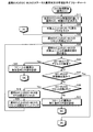
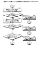
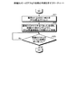
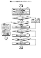
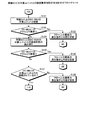
図15A〜図15Eは、運用SVCの異常ユニット判定処理の中の運用SVCの異常箇所判定の手順を示すフローチャートである。図15Aでは、運用SVCのI2C−MUXのステータス異常判定の手順を示す。図15Bでは、運用SVCの対象ユニットとの接続異常判定の手順を示す。図15Cでは、運用SVCの対象ユニットからの読取異常判定の手順を示す。図15Dでは、運用SVCの対象ユニットへの書込異常判定の手順を示す。図15Eでは、運用SVCの対象ユニットからの切断異常判定の手順を示す。なお、I2Cバス装置9は、運用中であるものとする。
FIG. 15A to FIG. 15E are flowcharts showing a procedure for determining an abnormal part of the operational SVC in the abnormal unit determination process of the operational SVC. FIG. 15A shows the procedure for determining the status abnormality of the I2C-MUX of the operational SVC. FIG. 15B shows a procedure for determining a connection abnormality with the target unit of the operational SVC. FIG. 15C shows a procedure for determining a reading abnormality from the target unit of the operational SVC. FIG. 15D shows a procedure for determining an abnormality in writing to the target unit of the operational SVC. FIG. 15E shows a procedure for determining disconnection abnormality from the target unit of the operational SVC. It is assumed that the
運用中であるI2Cバス装置9のI2Cマスタユニット1Aでは、異常箇所判定部31aが、他系のI2Cマスタユニット1Bとの間のFPGA間通信を用いて、運用SVCとなるか待機SVCとなるかを調停して決定する(ステップS11)。ここでは、I2Cマスタユニット1Aは、調停の結果、自ユニットが運用SVCとなると決定したものとする。そして、異常箇所判定部31aは、対象ユニットのリカバリ済みフラグをクリアする(ステップS12)。
In the
[運用SVC:I2C−MUXの接続状態異常判定]
続いて、異常箇所判定部31aは、運用SVC上のI2C−MUXのリセット回数を0にクリアする(ステップS13)。そして、異常箇所判定部31aは、I2Cシーケンス制御部32を介して、I2C−MUX20の接続状態(ステータス)を読み取る(ステップS14)。そして、異常箇所判定部31aは、I2C−MUX20へのアクセスで異常があるか否かを判定する(ステップS15)。I2C−MUX20へのアクセスで異常があると判定した場合(ステップS15;Yes)、異常箇所判定部31aは、異常の発生箇所と異常内容を含む異常種別をアクセス結果として記憶部40に保持する(ステップS16)。ここでは、異常の発生箇所をI2C−MUX20のステータスを確認する箇所とし、異常内容をI2Cシーケンス異常とする異常種別「e1」を記憶部40に保持する。その後、異常箇所判定部31aは、ステップS71からの「待機SVCへのアクセス依頼」に移行する。
[Operation SVC: I2C-MUX connection status abnormality determination]
Subsequently, the abnormal
一方、I2C−MUX20へのアクセスで異常がないと判定した場合(ステップS15:No)、異常箇所判定部31aは、I2C−MUX20が対象ユニット3と未接続状態であるか否かを判定する(ステップS17)。I2C−MUX20が対象ユニット3と未接続状態であると判定した場合(ステップS17;Yes)、異常箇所判定部31aは、ステップS31からの「対象ユニットとの接続異常判定」に移行する。
On the other hand, when it is determined that there is no abnormality in access to the I2C-MUX 20 (step S15: No), the abnormal
一方、I2C−MUX20が対象ユニット3と未接続状態でないと判定した場合(ステップS17;No)、異常箇所判定部31aは、期待した未接続状態となっていない。このため、異常箇所判定部31aは、I2C−MUX20のリセット回数が0であるか否かを判定する(ステップS18)。I2C−MUX20のリセット回数が0である場合(ステップS18;Yes)、異常箇所判定部31aは、運用SVC上のI2C−MUX20をFPGA経由でリセットする(ステップS19)。そして、異常箇所判定部31aは、運用SVC上のI2C−MUX20のリセット回数をカウントアップする(ステップS20)。その後、異常箇所判定部31aは、I2C−MUX20へのアクセスを再試行すべく、ステップS14に移行する。
On the other hand, when it is determined that the I2C-
一方、I2C−MUX20のリセット回数が0でない場合(ステップS18;No)、異常箇所判定部31aは、異常の発生箇所と異常内容を含む異常種別をアクセス結果として記憶部40に保持する(ステップS21)。ここでは、異常の発生箇所をI2C−MUX20のステータスを確認する箇所とし、異常内容をI2Cデバイス異常とする異常種別「e2」を記憶部40に保持する。その後、異常箇所判定部31aは、ステップS71からの「待機SVCへのアクセス依頼」に移行する。
On the other hand, when the number of resets of the I2C-
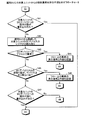
[運用SVC:対象ユニットとの接続異常判定]
次に、異常箇所判定部31aは、I2Cシーケンス制御部32を介して、運用SVC上のI2C−MUX20を対象ユニット3と接続する(ステップS31)。そして、異常箇所判定部31aは、I2C−MUX20へのアクセスで異常があるか否かを判定する(ステップS32)。I2C−MUX20へのアクセスで異常があると判定した場合(ステップS32;Yes)、異常箇所判定部31aは、異常の発生箇所と異常内容を含む異常種別をアクセス結果として記憶部40に保持する(ステップS33)。ここでは、異常の発生箇所をI2C−MUX20を対象ユニット3と接続する箇所とし、異常内容をI2Cシーケンス異常とする異常種別「e3」を記憶部40に保持する。その後、異常箇所判定部31aは、ステップS71からの「待機SVCへのアクセス依頼」に移行する。
[Operation SVC: Connection error judgment with the target unit]
Next, the abnormal
I2C−MUX20へのアクセスで異常がないと判定した場合(ステップS32;No)、異常箇所判定部31aは、運用SVC上のI2C−MUX20の対象ユニット3との接続状態を読み取る(ステップS34)。そして、異常箇所判定部31aは、I2C−MUX20へのアクセスで異常があるか否かを、I2C−MUX20のレジスタを用いて判定する(ステップS35)。I2C−MUX20へのアクセスで異常があると判定した場合(ステップS35;Yes)、異常箇所判定部31aは、異常の発生箇所と異常内容を含む異常種別をアクセス結果として記憶部40に保持する(ステップS36)。ここでは、異常の発生箇所をI2C−MUX20が対象ユニット3と接続したことを確認する箇所とし、異常内容をI2Cシーケンス異常とする異常種別「e4」を記憶部40に保持する。その後、異常箇所判定部31aは、ステップS71からの「待機SVCへのアクセス依頼」に移行する。
When it is determined that there is no abnormality in access to the I2C-MUX 20 (step S32; No), the abnormal
一方、I2C−MUX20へのアクセスで異常がないと判定した場合(ステップS35;No)、異常箇所判定部31aは、I2C−MUX20が対象ユニット3とのみ接続されているか否かを判定する(ステップS37)。I2C−MUX20が対象ユニット3とのみ接続されていないと判定した場合(ステップ37;No)、異常箇所判定部31aは、異常の発生箇所と異常内容を含む異常種別をアクセス結果として記憶部40に保持する(ステップS38)。ここでは、異常の発生箇所をI2C−MUX20が対象ユニット3と接続したことを確認する箇所とし、異常内容をI2Cデバイス異常とする異常種別「e5」を記憶部40に保持する。その後、異常箇所判定部31aは、ステップS71からの「待機SVCへのアクセス依頼」に移行する。
On the other hand, when it is determined that there is no abnormality in access to the I2C-MUX 20 (step S35; No), the abnormal
一方、I2C−MUX20が対象ユニット3とのみ接続されていると判定した場合(ステップS37;Yes)、異常箇所判定部31aは、ステップS41からの「対象ユニットからの読取異常判定」に移行する。
On the other hand, when it is determined that the I2C-
[運用SVC:対象ユニットからの読取異常判定]
次に、異常箇所判定部31aは、対象ユニット3のI2Cデバイスへの操作内容が書き込みのみか否かを判定する(ステップS41)。対象ユニット3のI2Cデバイスへの操作内容が書き込みのみであると判定した場合(ステップS41;Yes)、異常箇所判定部31aは、ステップS51からの「対象ユニットへの書込異常判定」に移行する。
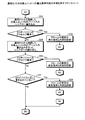
[Operation SVC: Reading abnormality determination from the target unit]
Next, the abnormal
一方、対象ユニット3のI2Cデバイスへの操作内容が書き込みのみでないと判定した場合(ステップS41;No)、異常箇所判定部31aは、運用SVC側から接続した対象ユニット3のI2Cデバイスのレジスタを読み取る(ステップS42)。そして、異常箇所判定部31aは、I2Cデバイスへのアクセスで異常があるか否かを判定する(ステップS43)。I2Cデバイスへのアクセスで異常があると判定した場合(ステップS43;Yes)、異常箇所判定部31aは、異常の発生箇所と異常内容を含む異常種別をアクセス結果として記憶部40に保持する(ステップS44)。ここでは、異常の発生箇所を対象ユニットとアクセスする箇所とし、異常内容をI2Cシーケンス異常とする異常種別「e6」を記憶部40に保持する。その後、異常箇所判定部31aは、ステップS71からの「待機SVCへのアクセス依頼」に移行する。
On the other hand, when it is determined that the operation content to the I2C device of the
一方、I2Cデバイスへのアクセスで異常がないと判定した場合(ステップS43;No)、異常箇所判定部31aは、I2Cデバイスからの読み取り値がI2Cデバイス上あり得ない値であるか否かを判定する(ステップS45)。I2Cデバイスからの読み取り値がI2Cデバイス上あり得ない値であると判定した場合(ステップS45;Yes)、異常箇所判定部31aは、異常の発生箇所と異常内容を含む異常種別をアクセス結果として記憶部40に保持する(ステップS46)。ここでは、異常の発生箇所を対象ユニットとアクセスする箇所とし、異常内容をI2Cデバイス異常とする異常種別「e7」を記憶部40に保持する。その後、異常箇所判定部31aは、ステップS71からの「待機SVCへのアクセス依頼」に移行する。
On the other hand, when it is determined that there is no abnormality in the access to the I2C device (step S43; No), the abnormal
一方、I2Cデバイスからの読み取り値がI2Cデバイス上あり得る値であると判定した場合(ステップS45;No)、異常箇所判定部31aは、対象ユニット3のI2Cデバイスへの操作内容に書き込みがあるか否かを判定する(ステップS47)。対象ユニット3のI2Cデバイスへの操作内容に書き込みがない(読み取りのみ)と判定した場合(ステップS47;No)、異常箇所判定部31aは、ステップS61からの「対象ユニットからの切断異常判定」に移行する。
On the other hand, when it is determined that the read value from the I2C device is a value that can be on the I2C device (step S45; No), the abnormal
一方、対象ユニット3のI2Cデバイスへの操作内容に書き込みがあると判定した場合(ステップS47;Yes)、異常箇所判定部31aは、ステップS51からの「対象ユニットへの書込異常判定」に移行する。
On the other hand, when it is determined that there is a write in the operation content of the
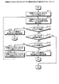
[運用SVC:対象ユニットへの書込異常判定]
次に、異常箇所判定部31aは、運用SVC側から接続した対象ユニット3のI2Cデバイスのレジスタへデータを書き込む(ステップS51)。そして、異常箇所判定部31aは、I2Cデバイスへのアクセスで異常があるか否かを判定する(ステップS52)。I2Cデバイスへのアクセスで異常があると判定した場合(ステップS52;Yes)、異常箇所判定部31aは、異常の発生箇所と異常内容を含む異常種別をアクセス結果として記憶部40に保持する(ステップS53)。ここでは、異常の発生箇所を対象ユニットとアクセスする箇所とし、異常内容をI2Cシーケンス異常とする異常種別「e6」を記憶部40に保持する。その後、異常箇所判定部31aは、ステップS71からの「待機SVCへのアクセス依頼」に移行する。
[Operation SVC: Judgment of abnormal writing to target unit]
Next, the abnormal
一方、I2Cデバイスへのアクセスで異常がないと判定した場合(ステップS52;No)、異常箇所判定部31aは、書き込んだデータを確認すべく、対象ユニット3のI2Cデバイスの書き込みを行ったレジスタを読み取る(ステップS54)。そして、異常箇所判定部31aは、I2Cデバイスへのアクセスで異常があるか否かを判定する(ステップS55)。I2Cデバイスへのアクセスで異常があると判定した場合(ステップS55;Yes)、異常箇所判定部31aは、異常の発生箇所と異常内容を含む異常種別をアクセス結果として記憶部40に保持する(ステップS56)。ここでは、異常の発生箇所を対象ユニットとアクセスする箇所とし、異常内容をI2Cシーケンス異常とする異常種別「e6」を記憶部40に保持する。その後、異常箇所判定部31aは、ステップS71からの「待機SVCへのアクセス依頼」に移行する。
On the other hand, when it is determined that there is no abnormality in the access to the I2C device (step S52; No), the abnormal
一方、I2Cデバイスへのアクセスで異常がないと判定した場合(ステップS55;No)、異常箇所判定部31aは、I2Cデバイスに正しく書き込めていないか否かを判定する(ステップS57)。具体的には、異常箇所判定部31aは、I2Cデバイスのレジスタへ書き込んだデータと、同一のレジスタから読み取ったデータを比較し、同一データでないか否かを判定すれば良い。そして、I2Cデバイスに正しく書き込めていないと判定した場合(ステップS57;Yes)、異常箇所判定部31aは、異常の発生箇所と異常内容を含む異常種別をアクセス結果として記憶部40に保持する(ステップS58)。ここでは、異常の発生箇所を対象ユニットとアクセスする箇所とし、異常内容をI2Cデバイス異常とする異常種別「e7」を記憶部40に保持する。その後、異常箇所判定部31aは、ステップS71からの「待機SVCへのアクセス依頼」に移行する。
On the other hand, when it is determined that there is no abnormality in the access to the I2C device (step S55; No), the abnormal
一方、I2Cデバイスに正しく書き込めていると判定した場合(ステップS57;No)、異常箇所判定部31aは、ステップS61からの「対象ユニットからの切断異常判定」に移行する。
On the other hand, when it is determined that the data is correctly written in the I2C device (step S57; No), the abnormal
[運用SVC:対象ユニットからの切断異常判定]
次に、異常箇所判定部31aは、I2Cシーケンス制御部32を介して、運用SVC上のI2C−MUX20を対象ユニット3から切断する(ステップS61)。そして、異常箇所判定部31aは、I2C−MUX20へのアクセスで異常があるか否かを判定する(ステップS62)。I2C−MUX20へのアクセスで異常があると判定した場合(ステップS62;Yes)、異常箇所判定部31aは、異常の発生箇所と異常内容を含む異常種別をアクセス結果として記憶部40に保持する(ステップS63)。ここでは、異常の発生箇所をI2C−MUX20を対象ユニット3から切断したことを確認する箇所とし、異常内容をI2Cシーケンス異常とする異常種別「e8」を記憶部40に保持する。その後、異常箇所判定部31aは、ステップS71からの「待機SVCへのアクセス依頼」に移行する。
[Operation SVC: Disconnection abnormality judgment from target unit]
Next, the abnormal
I2C−MUX20へのアクセスで異常があると判定した場合(ステップS62;No)、異常箇所判定部31aは、運用SVC上のI2C−MUX20の対象ユニット3との接続状態を読み取る(ステップS64)。そして、異常箇所判定部31aは、I2C−MUX20へのアクセスで異常があるか否かを、I2C−MUX20のレジスタを用いて判定する(ステップS65)。I2C−MUX20へのアクセスで異常があると判定した場合(ステップS65;Yes)、異常箇所判定部31aは、異常の発生箇所と異常内容を含む異常種別をアクセス結果として記憶部40に保持する(ステップS66)。ここでは、異常の発生箇所をI2C−MUX20を対象ユニット3から切断したことを確認する箇所とし、異常内容をI2Cシーケンス異常とする異常種別「e9」を記憶部40に保持する。その後、異常箇所判定部31aは、ステップS71からの「待機SVCへのアクセス依頼」に移行する。
When it is determined that there is an abnormality in the access to the I2C-MUX 20 (step S62; No), the abnormal
一方、I2C−MUX20へのアクセスで異常がないと判定した場合(ステップS65;No)、異常箇所判定部31aは、I2C−MUX20が未接続状態であるか否かを判定する(ステップS67)。I2C−MUX20が未接続状態でないと判定した場合(ステップS67;No)、期待した未接続状態となっていない。このため、異常箇所判定部31aは、異常の発生箇所と異常内容を含む異常種別をアクセス結果として記憶部40に保持する(ステップS68)。ここでは、異常の発生箇所をI2C−MUX20を対象ユニット3から切断したことを確認する箇所とし、異常内容をI2Cデバイス異常とする異常種別「e10」を記憶部40に保持する。その後、異常箇所判定部31aは、ステップS71からの「待機SVCへのアクセス依頼」に移行する。
On the other hand, when it is determined that there is no abnormality in accessing the I2C-MUX 20 (step S65; No), the abnormal
一方、I2C−MUX20が未接続状態である場合(ステップS67;Yes)または異常ユニット判定部31cが待機SVCからアクセス結果を受け取った場合(ステップS73;Yes)、異常箇所判定部31aは、以下の処理を行う。すなわち、異常箇所判定部31aは、運用SVCが対象ユニット3との接続で異常が発生したか否かを判定する(ステップS69)。例えば、異常箇所判定部31aは、記憶部40に運用SVCの正常以外の異常種別が保持されているか否かを判定すれば良い。そして、運用SVCが対象ユニット3との接続で異常が発生したと判定した場合(ステップS69;Yes)、異常箇所判定部31aは、ステップS81からの「異常ユニット判定」に移行する。一方、運用SVCが対象ユニット3との接続で異常が発生しなかった場合(ステップS69;No)、または異常ユニットの判定が完了した場合、異常箇所判定部31aは、異常ユニット判定処理を終了する。
On the other hand, when the I2C-
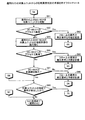
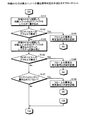
[運用SVC:待機SVCへのアクセス依頼]
図16は、待機SVCへのアクセス依頼の手順を示すフローチャートである。
[Operation SVC: Request for access to standby SVC]
FIG. 16 is a flowchart showing the procedure for requesting access to the standby SVC.
異常箇所判定部31aによって対象ユニット3への接続、すなわちアクセスで異常箇所があった場合に、アクセス依頼部31bは、運用SVC上のI2C−MUX20をFPGA経由でリセットする(ステップS71)。これは、待機SVCでの動作に影響を与えないためである。
When there is an abnormal location in the connection to the
そして、アクセス依頼部31bは、運用SVCが行う予定であった処理を、待機SVC側から行うように、FPGA間通信経由で待機SVCに依頼する(ステップS72)。すなわち、アクセス依頼部31bは、運用SVCにおいてアクセスが異常となった対象ユニットへのアクセスを、待機SVCに依頼する。
Then, the
そして、異常ユニット判定部31cは、FPGA間通信経由で送られるてくる待機SVCのアクセス結果を受け取ったか否かを判定する(ステップS73)。待機SVCのアクセス結果を受け取っていないと判定した場合(ステップS73;No)、異常ユニット判定部31cは、再度判定すべく、ステップS73に移行する。そして、待機SVCのアクセス結果を受け取ったと判定した場合(ステップS73;Yes)、異常ユニット判定部31cは、異常ユニット判定をすべく、ステップS69に移行する。 Then, the abnormal unit determination unit 31c determines whether or not an access result of the standby SVC sent via the inter-FPGA communication has been received (step S73). If it is determined that the access result of the standby SVC has not been received (step S73; No), the abnormal unit determination unit 31c proceeds to step S73 to make a determination again. And when it determines with having received the access result of standby SVC (step S73; Yes), the abnormal unit determination part 31c transfers to step S69 in order to perform abnormal unit determination.
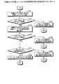
[運用SVC:異常ユニット判定]
図17は、異常ユニット判定の手順を示すフローチャートである。
[Operation SVC: Abnormal unit determination]
FIG. 17 is a flowchart illustrating the procedure for determining an abnormal unit.
待機SVCからアクセス結果を受け取った場合に、異常ユニット判定部31cは、異常ユニット判定マトリクス41を用いて、異常ユニットを判定する(ステップS81)。すなわち、異常ユニット判定部31cは、運用SVC上での対象ユニット3へのアクセス結果を横軸とし、待機SVC上での対象ユニット3へのアクセス結果を縦軸とした異常ユニット判定マトリクス41で異常ユニットを判定する。一例として、異常ユニット判定部31cは、異常ユニット判定マトリクス41に記憶された、運用SVCと待機SVCとのそれぞれの異常判定情報の組み合わせと、それぞれのアクセス結果の組み合わせとを用いて、異常ユニットを判定する。
When the access result is received from the standby SVC, the abnormal unit determination unit 31c determines an abnormal unit using the abnormal unit determination matrix 41 (step S81). In other words, the abnormal unit determination unit 31c generates an error in the abnormal
そして、異常ユニット判定部31cは、判定の結果、異常ユニットが対象ユニット3であるか否かを判定する(ステップS82)。異常ユニットが対象ユニット3でない、すなわち運用SVCまたは待機SVCであると判定した場合(ステップS82;No)、異常ユニット判定部31cは、対象ユニットのリカバリ済みフラグを0にクリアする(ステップS83)。その後、異常ユニット判定部31cは、さらに異常ユニットを判別すべく、ステップS88に移行する。
And the abnormal unit determination part 31c determines whether an abnormal unit is the
一方、異常ユニットが対象ユニット3であると判定した場合(ステップS82;Yes)、異常ユニット判定部31cは、対象ユニットのリカバリ済みフラグを用いて、リカバリ済みであるか否かを判定する(ステップS84)。リカバリ済みであると判定した場合(ステップS84;Yes)、異常ユニット判定部31cは、対象ユニットを異常ユニットとして確定する(ステップS85)。 On the other hand, when it is determined that the abnormal unit is the target unit 3 (step S82; Yes), the abnormal unit determination unit 31c determines whether it has been recovered using the recovered flag of the target unit (step S82). S84). When it determines with having recovered (step S84; Yes), the abnormal unit determination part 31c determines a target unit as an abnormal unit (step S85).
一方、リカバリ済みでないと判定した場合(ステップS84;No)、異常ユニット判定部31cは、運用SVC上のFPGAから対象ユニット3のI2Cデバイスをリセットする(ステップS86)。そして、異常ユニット判定部31cは、対象ユニットのリカバリ済みフラグを設定する(ステップS87)。その後、異常ユニット判定部31cは、対象ユニット3へのアクセスを再試行すべく、ステップS13に移行する。
On the other hand, when it is determined that the recovery has not been completed (step S84; No), the abnormal unit determination unit 31c resets the I2C device of the
さらに、異常ユニットが対象ユニット3でない場合に、ステップS83の処理後、異常ユニット判定部31cは、異常ユニットが運用SVCであるか否かを判定する(ステップS88)。異常ユニットが運用SVCであると判定した場合(ステップS88;Yes)。異常ユニット判定部31cは、運用SVCを異常ユニットとして確定する(ステップS89)。
Furthermore, when the abnormal unit is not the
一方、異常ユニットが運用SVCでないと判定した場合(ステップS88;No)、異常ユニット判定部31cは、異常ユニットが待機SVCであるか否かを判定する(ステップS90)。異常ユニットが待機SVCであると判定した場合(ステップS90;Yes)。異常ユニット判定部31cは、待機SVCを異常ユニットとして確定する(ステップS91)。その後、異常ユニット判定部31cは、異常ユニット判定処理を終了する。また、異常ユニットが待機SVCでないと判定した場合も(ステップS90;No)、その後、異常ユニット判定部31cは、異常ユニット判定処理を終了する。 On the other hand, when it is determined that the abnormal unit is not an operational SVC (step S88; No), the abnormal unit determination unit 31c determines whether the abnormal unit is a standby SVC (step S90). When it is determined that the abnormal unit is a standby SVC (step S90; Yes). The abnormal unit determination unit 31c determines the standby SVC as an abnormal unit (step S91). Thereafter, the abnormal unit determination unit 31c ends the abnormal unit determination process. Moreover, also when it determines with an abnormal unit not being standby SVC (step S90; No), after that, the abnormal unit determination part 31c complete | finishes an abnormal unit determination process.
[待機SVC:アクセス依頼待ち]
図18は、待機SVCのアクセス依頼待ちの手順を示すフローチャートである。
[Stand-by SVC: Waiting for access request]
FIG. 18 is a flowchart showing a procedure for waiting for an access request of a standby SVC.
まず、I2Cマスタユニット1Bでは、異常箇所判定部31aが、他系のI2Cマスタユニット1Aとの間のSPGA間通信を用いて、運用SVCとなるか待機SVCとなるかを調停して決定する(ステップS101)。ここでは、I2Cマスタユニット1Bは、I2Cマスタユニット1Aとの調停の結果、自ユニットが待機SVCとなると決定したものとする。
First, in the
そして、異常箇所判定部31aは、対象ユニット3へのアクセス依頼を受け取ったか否かを判定する(ステップS102)。すなわち、異常箇所判定部31aは、運用SVCが行う予定であった処理のアクセス依頼をPFGA間通信経由で受け取りを待ち合わせる。対象ユニット3へのアクセス依頼を受け取っていないと判定した場合(ステップS102;No)、異常箇所判定部31aは、再度判定すべく、ステップS102に移行する。そして、対象ユニット3へのアクセス依頼を受け取ったと判定した場合(ステップS102;Yes)、ステップS111からの「I2C−MUXの接続状態異常判定」に移行する。
And the abnormal
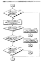
図19A〜図19Eは、待機SVCの異常ユニット判定処理の中の待機SVCの異常箇所判定の手順を示すフローチャートである。図19Aでは、待機SVCのI2C−MUXのステータス異常判定の手順を示す。図19Bでは、待機SVCの対象ユニットとの接続異常判定の手順を示す。図19Cでは、待機SVCの対象ユニットからの読取異常判定の手順を示す。図19Dでは、待機SVCの対象ユニットへの書込異常判定の手順を示す。図19Eでは、待機SVCの対象ユニットからの切断異常判定の手順を示す。なお、異常箇所判定部31aは、対象ユニット3へのアクセス依頼を運用SVCから受け取ったものとする。
FIG. 19A to FIG. 19E are flowcharts showing a procedure for determining an abnormal point of the standby SVC in the abnormal unit determination process of the standby SVC. FIG. 19A shows a procedure for determining the status abnormality of the I2C-MUX of the standby SVC. FIG. 19B shows a procedure for determining a connection abnormality with the target unit of the standby SVC. FIG. 19C shows a procedure for determining a reading abnormality from the target unit of the standby SVC. FIG. 19D shows a procedure for determining a writing abnormality in the target unit of the standby SVC. FIG. 19E shows a procedure for determining disconnection abnormality from the target unit of the standby SVC. It is assumed that the abnormal
[待機SVC:I2C−MUXの接続状態異常判定]
対象ユニット3へのアクセス依頼を受け取った異常箇所判定部31aは、待機SVC上のI2C−MUXのリセット回数を0にクリアする(ステップS111)。そして、異常箇所判定部31aは、I2Cシーケンス制御部32を介して、I2C−MUX20の接続状態(ステータス)を読み取る(ステップS112)。そして、異常箇所判定部31aは、I2C−MUX20へのアクセスで異常があるか否かを判定する(ステップS113)。I2C−MUX20へのアクセスで異常があると判定した場合(ステップS113;Yes)、異常箇所判定部31aは、異常の発生箇所と異常内容を含む異常種別をアクセス結果として記憶部40に保持する(ステップS114)。ここでは、異常の発生箇所をI2C−MUX20のステータスを確認する箇所とし、異常内容をI2Cシーケンス異常とする異常種別「e1」を記憶部40に保持する。その後、異常箇所判定部31aは、ステップS161からの「運用SVCへのアクセス結果通知」に移行する。
[Standby SVC: I2C-MUX connection status abnormality determination]
Receiving the access request to the
一方、I2C−MUX20へのアクセスで異常がないと判定した場合(ステップS113:No)、異常箇所判定部31aは、I2C−MUX20が対象ユニット3と未接続状態であるか否かを判定する(ステップS115)。I2C−MUX20が対象ユニット3と未接続状態であると判定した場合(ステップS115;Yes)、異常箇所判定部31aは、ステップS121からの「対象ユニットとの接続異常判定」に移行する。
On the other hand, when it is determined that there is no abnormality in accessing the I2C-MUX 20 (step S113: No), the abnormal
一方、I2C−MUX20が対象ユニット3と未接続状態でないと判定した場合(ステップS115;No)、異常箇所判定部31aは、期待した未接続状態となっていない。このため、異常箇所判定部31aは、I2C−MUX20Aのリセット回数が0であるか否かを判定する(ステップS116)。I2C−MUX20Aのリセット回数が0である場合(ステップS116;Yes)、異常箇所判定部31aは、待機SVC上のI2C−MUX20をFPGA経由でリセットする(ステップS117)。そして、異常箇所判定部31aは、待機SVC上のI2C−MUX20のリセット回数をカウントアップする(ステップS118)。その後、異常箇所判定部31aは、I2C−MUX20へのアクセスを再試行すべく、ステップS112に移行する。
On the other hand, when it is determined that the I2C-
一方、I2C−MUX20のリセット回数が0でない場合(ステップS116;No)、異常箇所判定部31aは、異常の発生箇所と異常内容を含む異常種別をアクセス結果として記憶部40に保持する(ステップS119)。ここでは、異常の発生箇所をI2C−MUX20のステータスを確認する箇所とし、異常内容をI2Cデバイス異常とする異常種別「e2」を記憶部40に保持する。その後、異常箇所判定部31aは、ステップS161からの「運用SVCへのアクセス結果通知」に移行する。
On the other hand, when the number of resets of the I2C-
[待機SVC:対象ユニットとの接続異常判定]
次に、異常箇所判定部31aは、I2Cシーケンス制御部32を介して、待機SVC上のI2C−MUX20を対象ユニット3と接続する(ステップS121)。そして、異常箇所判定部31aは、I2C−MUX20へのアクセスで異常があるか否かを判定する(ステップS122)。I2C−MUX20へのアクセスで異常があると判定した場合(ステップS122;Yes)、異常箇所判定部31aは、異常の発生箇所と異常内容を含む異常種別をアクセス結果として記憶部40に保持する(ステップS123)。ここでは、異常の発生箇所をI2C−MUX20を対象ユニット3と接続する箇所とし、異常内容をI2Cシーケンス異常とする異常種別「e3」を記憶部40に保持する。その後、異常箇所判定部31aは、ステップS161からの「運用SVCへのアクセス結果通知」に移行する。
[Standby SVC: Connection error determination with target unit]
Next, the abnormal
I2C−MUX20へのアクセスで異常がないと判定した場合(ステップS122;No)、異常箇所判定部31aは、待機SVC上のI2C−MUX20の対象ユニット3との接続状態を読み取る(ステップS124)。そして、異常箇所判定部31aは、I2C−MUX20へのアクセスで異常があるか否かを、I2C−MUX20のレジスタを用いて判定する(ステップS125)。I2C−MUX20へのアクセスで異常があると判定した場合(ステップS125;Yes)、異常箇所判定部31aは、異常の発生箇所と異常内容を含む異常種別をアクセス結果として記憶部40に保持する(ステップS126)。ここでは、異常の発生箇所をI2C−MUX20が対象ユニット3と接続したことを確認する箇所とし、異常内容をI2Cシーケンス異常とする異常種別「e4」を記憶部40に保持する。その後、異常箇所判定部31aは、ステップS161からの「運用SVCへのアクセス結果通知」に移行する。
When it is determined that there is no abnormality in access to the I2C-MUX 20 (step S122; No), the abnormal
一方、I2C−MUX20へのアクセスで異常がないと判定した場合(ステップS125;No)、異常箇所判定部31aは、I2C−MUX20が対象ユニット3とのみ接続されているか否かを判定する(ステップS127)。I2C−MUX20が対象ユニット3とのみ接続されていないと判定した場合(ステップ127;No)、異常箇所判定部31aは、異常の発生箇所と異常内容を含む異常種別をアクセス結果として記憶部40に保持する(ステップS128)。ここでは、異常の発生箇所をI2C−MUX20が対象ユニット3と接続したことを確認する箇所とし、異常内容をI2Cデバイス異常とする異常種別「e5」を記憶部40に保持する。その後、異常箇所判定部31aは、ステップS161からの「運用SVCへのアクセス結果通知」に移行する。
On the other hand, when it is determined that there is no abnormality in access to the I2C-MUX 20 (step S125; No), the abnormal
一方、I2C−MUX20が対象ユニット3とのみ接続されていると判定した場合(ステップS127;Yes)、異常箇所判定部31aは、ステップS131からの「対象ユニットからの読取異常判定」に移行する。
On the other hand, when it is determined that the I2C-
[待機SVC:対象ユニットからの読取異常判定]
次に、異常箇所判定部31aは、対象ユニット3のI2Cデバイスへの操作内容が書き込みのみか否かを判定する(ステップS131)。対象ユニット3のI2Cデバイスへの操作内容が書き込みのみであると判定した場合(ステップS131;Yes)、異常箇所判定部31aは、ステップS141からの「対象ユニットへの書込異常判定」に移行する。
[Stand-by SVC: Reading abnormality determination from the target unit]
Next, the abnormal
一方、対象ユニット3のI2Cデバイスへの操作内容が書き込みのみでないと判定した場合(ステップS131;No)、異常箇所判定部31aは、待機SVC側から接続した対象ユニット3のI2Cデバイスのレジスタを読み取る(ステップS132)。そして、異常箇所判定部31aは、I2Cデバイスへのアクセスで異常があるか否かを判定する(ステップS133)。I2Cデバイスへのアクセスで異常があると判定した場合(ステップS133;Yes)、異常箇所判定部31aは、異常の発生箇所と異常内容を含む異常種別をアクセス結果として記憶部40に保持する(ステップS134)。ここでは、異常の発生箇所を対象ユニットとアクセスする箇所とし、異常内容をI2Cシーケンス異常とする異常種別「e6」を記憶部40に保持する。その後、異常箇所判定部31aは、ステップS161からの「運用SVCへのアクセス結果通知」に移行する。
On the other hand, when it is determined that the operation content of the
一方、I2Cデバイスへのアクセスで異常がないと判定した場合(ステップS133;No)、異常箇所判定部31aは、I2Cデバイスからの読み取り値がI2Cデバイス上あり得ない値であるか否かを判定する(ステップS135)。I2Cデバイスからの読み取り値がI2Cデバイス上あり得ない値であると判定した場合(ステップS135;Yes)、異常箇所判定部31aは、異常の発生箇所と異常内容を含む異常種別をアクセス結果として記憶部40に保持する(ステップS136)。ここでは、異常の発生箇所を対象ユニットとアクセスする箇所とし、異常内容をI2Cデバイス異常とする異常種別「e7」を記憶部40に保持する。その後、異常箇所判定部31aは、ステップS161からの「運用SVCへのアクセス結果通知」に移行する。
On the other hand, when it is determined that there is no abnormality in the access to the I2C device (step S133; No), the abnormal
一方、I2Cデバイスからの読み取り値がI2Cデバイス上あり得ない値でないと判定した場合(ステップS135;No)、異常箇所判定部31aは、対象ユニット3のI2Cデバイスへの操作内容に書き込みがあるか否かを判定する(ステップS137)。対象ユニット3のI2Cデバイスへの操作内容に書き込みがない(読み取りのみ)と判定した場合(ステップS137;No)、異常箇所判定部31aは、ステップS141からの「対象ユニットからの切断異常判定」に移行する。
On the other hand, when it is determined that the read value from the I2C device is not a value that is not possible on the I2C device (step S135; No), the abnormal
一方、対象ユニット3のI2Cデバイスへの操作内容に書き込みがあると判定した場合(ステップS137;Yes)、異常箇所判定部31aは、ステップS141からの「対象ユニットへの書込異常判定」に移行する。
On the other hand, when it is determined that there is a write in the operation content of the
[待機SVC:対象ユニットへの書込異常判定]
次に、異常箇所判定部31aは、待機SVC側から接続した対象ユニット3のI2Cデバイスのレジスタへデータを書き込む(ステップS141)。そして、異常箇所判定部31aは、I2Cデバイスへのアクセスで異常があるか否かを判定する(ステップS142)。I2Cデバイスへのアクセスで異常があると判定した場合(ステップS142;Yes)、異常箇所判定部31aは、異常の発生箇所と異常内容を含む異常種別をアクセス結果として記憶部40に保持する(ステップS143)。ここでは、異常の発生箇所を対象ユニットとアクセスする箇所とし、異常内容をI2Cシーケンス異常とする異常種別「e6」を記憶部40に保持する。その後、異常箇所判定部31aは、ステップS161からの「運用SVCへのアクセス結果通知」に移行する。
[Stand-by SVC: Judgment of abnormal writing to target unit]
Next, the abnormal
一方、I2Cデバイスへのアクセスで異常がないと判定した場合(ステップS142;No)、異常箇所判定部31aは、書き込んだデータを確認すべく、対象ユニット3のI2Cデバイスの書き込みを行ったレジスタを読み取る(ステップS144)。そして、異常箇所判定部31aは、I2Cデバイスへのアクセスで異常があるか否かを判定する(ステップS145)。I2Cデバイスへのアクセスで異常があると判定した場合(ステップS145;Yes)、異常箇所判定部31aは、異常の発生箇所と異常内容を含む異常種別をアクセス結果として記憶部40に保持する(ステップS146)。ここでは、異常の発生箇所を対象ユニットとアクセスする箇所とし、異常内容をI2Cシーケンス異常とする異常種別「e6」を記憶部40に保持する。その後、異常箇所判定部31aは、ステップS161からの「運用SVCへのアクセス結果通知」に移行する。
On the other hand, when it is determined that there is no abnormality in the access to the I2C device (step S142; No), the abnormal
一方、I2Cデバイスへのアクセスで異常がないと判定した場合(ステップS145;No)、異常箇所判定部31aは、I2Cデバイスに正しく書き込めていないか否かを判定する(ステップS147)。具体的には、異常箇所判定部31aは、I2Cデバイスのレジスタへ書き込んだデータと、同一のレジスタから読み取ったデータを比較し、同一データでないか否かを判定すれば良い。そして、I2Cデバイスに正しく書き込めていないと判定した場合(ステップS147;Yes)、異常箇所判定部31aは、異常の発生箇所と異常内容を含む異常種別をアクセス結果として記憶部40に保持する(ステップS148)。ここでは、異常の発生箇所を対象ユニットとアクセスする箇所とし、異常内容をI2Cデバイス異常とする異常種別「e7」を記憶部40に保持する。その後、異常箇所判定部31aは、ステップS161からの「運用SVCへのアクセス結果通知」に移行する。
On the other hand, when it is determined that there is no abnormality in the access to the I2C device (step S145; No), the abnormal
一方、I2Cデバイスに正しく書き込めていると判定した場合(ステップS147;No)、異常箇所判定部31aは、ステップS151からの「対象ユニットからの切断異常判定」に移行する。
On the other hand, when it is determined that data is correctly written in the I2C device (step S147; No), the abnormal
[待機SVC:対象ユニットからの切断異常判定]
次に、異常箇所判定部31aは、I2Cシーケンス制御部32を介して、待機SVC上のI2C−MUX20を対象ユニット3から切断する(ステップS151)。そして、異常箇所判定部31aは、I2C−MUX20へのアクセスで異常があるか否かを判定する(ステップS152)。I2C−MUX20へのアクセスで異常があると判定した場合(ステップS152;Yes)、異常箇所判定部31aは、異常の発生箇所と異常内容を含む異常種別をアクセス結果として記憶部40に保持する(ステップS153)。ここでは、異常の発生箇所をI2C−MUX20を対象ユニット3から切断したことを確認する箇所とし、異常内容をI2Cシーケンス異常とする異常種別「e8」を記憶部40に保持する。その後、異常箇所判定部31aは、ステップS161からの「運用SVCへのアクセス結果通知」に移行する。
[Stand-by SVC: Disconnection abnormality judgment from target unit]
Next, the abnormal
I2C−MUX20へのアクセスで異常があると判定した場合(ステップS152;No)、異常箇所判定部31aは、待機SVC上のI2C−MUX20の対象ユニット3との接続状態を読み取る(ステップS154)。そして、異常箇所判定部31aは、I2C−MUX20へのアクセスで異常があるか否かを、I2C−MUX20のレジスタを用いて判定する(ステップS155)。I2C−MUX20へのアクセスで異常があると判定した場合(ステップS155;Yes)、異常箇所判定部31aは、異常の発生箇所と異常内容を含む異常種別をアクセス結果として記憶部40に保持する(ステップS156)。ここでは、異常の発生箇所をI2C−MUX20を対象ユニット3から切断したことを確認する箇所とし、異常内容をI2Cシーケンス異常とする異常種別「e9」を記憶部40に保持する。その後、異常箇所判定部31aは、ステップS161からの「運用SVCへのアクセス結果通知」に移行する。
When it is determined that there is an abnormality in access to the I2C-MUX 20 (step S152; No), the abnormal
一方、I2C−MUX20へのアクセスで異常がないと判定した場合(ステップS155;No)、異常箇所判定部31aは、I2C−MUX20が未接続状態であるか否かを判定する(ステップS157)。I2C−MUX20が未接続状態でないと判定した場合(ステップS157;No)、期待した未接続状態となっていない。このため、異常箇所判定部31aは、異常の発生箇所と異常内容を含む異常種別をアクセス結果として記憶部
40に保持する(ステップS158)。ここでは、異常の発生箇所をI2C−MUX20を対象ユニット3から切断したことを確認する箇所とし、異常内容をI2Cデバイス異常とする異常種別「e10」を記憶部40に保持する。その後、異常箇所判定部31aは、ステップS161からの「運用SVCへのアクセス結果通知」に移行する。
On the other hand, when it is determined that there is no abnormality in access to the I2C-MUX 20 (step S155; No), the abnormal
一方、I2C−MUX20が未接続状態でない場合(ステップS157;Yes)、異常箇所判定部31aは、対象ユニット3とのアクセスが正常であったことを記憶部40に保持する(ステップS159)。その後、異常箇所判定部31aは、ステップS162からの「運用SVCへのアクセス結果通知」に移行する。
On the other hand, when the I2C-
[待機SVC:運用SVCへのアクセス結果通知]
図20は、運用SVCへのアクセス結果通知の手順を示すフローチャートである。
[Standby SVC: Notification of Access Result to Operational SVC]
FIG. 20 is a flowchart showing the procedure for notifying the result of access to the operational SVC.
続いて、対象ユニット3とのアクセスが異常であった場合には、異常箇所判定部31aは、待機SVC上のI2C−MUX20をFPGA経由でリセットする(ステップS161)。なお、対象ユニット3とのアクセスが正常であった場合には、異常箇所判定部31aは、待機SVC上のI2C−MUX20をリセットしない。
Subsequently, when the access to the
そして、異常箇所判定部31aは、記憶部40に保持された処理結果(アクセス結果)をPFGA間通信経由で運用SVCに通知し(ステップS162)、待機SVCでの異常ユニット判定処理を終了する。
Then, the abnormal
[実施例の効果]
上記実施例によれば、I2Cバス装置9は、I2Cマスタユニット1Aと、I2Cマスタユニット1Aと二重化されたI2Cマスタユニット1Bとを有する。そして、I2Cマスタユニット1AおよびI2Cマスタユニット1Bは、I2Cバスで接続する複数のI2Cスレーブユニット3を制御する。さらに、I2Cマスタユニット1Aは、I2Cスレーブユニット3へのアクセスで異常を検出したとき、異常を検出した箇所に関するアクセス結果と、I2Cマスタユニット1Bからのアクセス結果との組み合わせを用いて、異常であるユニットを判定する。かかる構成によれば、I2Cバス装置9は、異常を検出されたI2Cスレーブユニット3に対する2個のアクセス結果の組み合わせを用いて、異常であるユニットを判定するので、どのユニットに異常があるのかを判定できる。例えば、I2Cバス装置9は、2個のアクセス結果が同じ箇所の異常である場合には、I2Cマスタユニット1A、1Bに異常はなく、I2Cスレーブユニット3に異常があることを判定できる。また、I2Cバス装置9は、I2Cマスタユニット1Aに異常があってもI2Cマスタユニット1Bに異常がない場合は、I2Cマスタユニット1Aに異常があることを判定できる。
[Effect of Example]
According to the above embodiment, the
また、上記実施例によれば、I2Cバス装置9では、異常箇所判定部31aが、自ユニットと接続されたI2Cスレーブユニット3へのアクセスで異常箇所があるか否かを判定する。そして、アクセス依頼部31bが、異常箇所判定部31aによってI2Cスレーブユニット3へのアクセスで異常箇所があると判定された場合に、I2Cスレーブユニット3と同一のI2Cスレーブユニット3へのアクセスを、I2Cマスタユニット1Bに依頼する。さらに、異常ユニット判定部31cは、異常箇所判定部31aによって異常箇所があると判定された異常箇所に関するアクセス結果とアクセス依頼部31bによる依頼の結果を示すアクセス結果との組み合わせを用いて、異常であるユニットを判定する。かかる構成によれば、異常箇所判定部31aは、異常箇所があると判定されたアクセス結果とアクセス依頼部31bによる依頼の結果を示すアクセス結果との組み合わせを用いて、異常であるユニットを判定するので、どのユニットに異常があるのかを判定できる。
Further, according to the above embodiment, in the
また、上記実施例によれば、I2Cマスタユニット1Aは、異常ユニット判定マトリクス41を有する。異常ユニット判定マトリクス41は、マスタユニットで異常となる可能性のある異常箇所に関する異常判定情報について、二重化されたマスタユニットの一方の異常判定情報と他方の異常判定情報との組み合わせにより異常と判定されるユニットの候補を記憶する。そして、異常ユニット判定部31cは、さらに、異常ユニット判定マトリクス41に記憶された、二重化されたマスタユニットのそれぞれの異常判定情報の組み合わせを用いて、I2Cスレーブユニット3へのアクセスで異常の原因となったユニットを判定する。かかる構成によれば、異常ユニット判定部31cは、異常ユニット判定マトリクス41に記憶された異常判定情報の組み合わせを細分化して記憶すると、異常であるユニットの判定をより正確に行うことができる。
Further, according to the above embodiment, the
また、上記実施例によれば、異常箇所に関する異常判定情報は、異常となる可能性のある箇所および当該箇所での異常内容を含む。かかる構成によれば、異常判定情報は、1個の異常となる可能性のある箇所に対して複数の異常内容を含ませることが可能となるので、異常判定情報のバリエーションを増やすことができる。この結果、異常ユニット判定部31cは、異常であるユニットの判定をさらに正確に行うことができる。 Further, according to the above-described embodiment, the abnormality determination information regarding the abnormal part includes a part that may become abnormal and the abnormality content at the part. According to such a configuration, the abnormality determination information can include a plurality of abnormality contents with respect to a place where there is a possibility of one abnormality, so that variations of the abnormality determination information can be increased. As a result, the abnormal unit determination unit 31c can more accurately determine an abnormal unit.
[その他]
なお、本実施例では、I2Cバス装置1が運用中に、運用SVCであるI2Cマスタユニット1Aが対象ユニット3へのアクセスで異常があった場合に、異常ユニットを判定するものとして説明した。しかしながら、これに限定されるものではなく、I2Cバス装置1が運用中でない場合であっても、異常ユニット判定処理を行っても良い。例えば、I2Cバス装置1が事前にI2Cバス間のユニットの故障診断を行う場合であっても良い。
[Others]
In this embodiment, the
また、図示した各装置の各構成要素は、必ずしも物理的に図示の如く構成されていることを要しない。すなわち、各装置の分散・統合の具体的態様は図示のものに限られず、その全部又は一部を、各種の負荷や使用状況等に応じて、任意の単位で機能的又は物理的に分散・統合して構成することができる。例えば、アクセス依頼部31bと異常ユニット判定部31cとを1つの部として統合しても良い。また、I2Cデバイス制御部31に備えられた各種機能部を1つの部として統合しても良い。一方、異常箇所判定部31aに備えられた各種機能をそれぞれ分散しても良い。一例として、異常箇所判定部31aを、運用系となるか待機系となるかを調停する調停部と、運用系と調停された場合の異常箇所判定部と、待機系と調停された場合の異常箇所判定部とに分散しても良い。この場合、待機系と調停された場合の異常箇所判定部を、運用系からのアクセス依頼を待ち受ける待受部と、異常箇所判定部と、アクセス結果を通知する通知部とに分散しても良い。また、記憶部40をI2Cバス装置9の外部装置としてネットワーク経由で接続するようにしても良い。
In addition, each component of each illustrated apparatus does not necessarily need to be physically configured as illustrated. That is, the specific mode of distribution / integration of each device is not limited to that shown in the figure, and all or a part thereof may be functionally or physically distributed or arbitrarily distributed in arbitrary units according to various loads or usage conditions. Can be integrated and configured. For example, the
また、I2Cバス装置9にて行われる各処理機能は、その全部または任意の一部が、CPU(またはMPU、MCU(Micro Controller Unit)などのマイクロ・コンピュータ)あるいは、ワイヤードロジックによるハードウェアとして実現されても良い。また、I2Cバス装置9にて行われる各処理機能は、その全部または任意の一部が、CPU(またはMPU、MCUなどのマイクロ・コンピュータ)にて解析実行されるプログラムにて実現されても良い。
Each processing function performed in the
以上の実施例に係る実施形態に関し、さらに以下の付記を開示する。 The following additional remarks are disclosed regarding the embodiment according to the above example.
(付記1)シリアルバスで接続する複数のスレーブユニットを制御する第1のマスタユニットと、
前記複数のスレーブユニットを制御し、前記第1のマスタユニットと二重化された第2のマスタユニットとを有し、
前記第1のマスタユニットは、
自ユニットと接続された前記スレーブユニットへのアクセスで異常を検出したとき、異常を検出した箇所に関するアクセス結果と、前記第2のマスタユニットと接続された前記スレーブユニットへの前記第2のマスタユニットからのアクセス結果とを用いて、異常であるユニットを判定する制御部
を有することを特徴とする情報処理装置。
(Supplementary note 1) a first master unit for controlling a plurality of slave units connected by a serial bus;
The plurality of slave units are controlled, and the first master unit and the second master unit are duplicated,
The first master unit is
When an abnormality is detected in access to the slave unit connected to the own unit, the access result regarding the location where the abnormality is detected, and the second master unit to the slave unit connected to the second master unit An information processing apparatus comprising: a control unit that determines an abnormal unit by using an access result from.
(付記2)前記制御部は、
自ユニットと接続された前記スレーブユニットへのアクセスで異常箇所があるか否かを判定する異常箇所判定部と、
前記異常箇所判定部によって前記スレーブユニットへのアクセスで異常箇所があると判定された場合に、前記スレーブユニットと同一のスレーブユニットへのアクセスを、前記第2のマスタユニットに依頼するアクセス依頼部と、
前記異常箇所判定部によって異常箇所があると判定された異常箇所に関するアクセス結果と前記アクセス依頼部による依頼の結果を示すアクセス結果との組み合わせを用いて、異常であるユニットを判定する異常ユニット判定部と
を有することを特徴とする付記1に記載の情報処理装置。
(Appendix 2) The control unit
An abnormal point determination unit that determines whether there is an abnormal point in accessing the slave unit connected to the own unit;
An access requesting unit for requesting the second master unit to access the same slave unit as the slave unit when the abnormal part determining unit determines that there is an abnormal part in accessing the slave unit; ,
An abnormal unit determination unit that determines a unit that is abnormal by using a combination of an access result related to an abnormal point determined to have an abnormal point by the abnormal point determination unit and an access result indicating a result of a request by the access request unit The information processing apparatus according to
(付記3)前記第1のマスタユニットは、
前記スレーブユニットへのアクセスでマスタユニット中の異常となる可能性のある箇所に関するアクセス情報について、二重化されたマスタユニットの一方の前記アクセス情報と他方の前記アクセス情報との組み合わせにより異常と判定されるユニットの候補を記憶する記憶部を有し、
前記異常ユニット判定部は、
さらに、前記記憶部に記憶された、二重化されたマスタユニットのそれぞれの前記アクセス情報の組み合わせを用いて、前記スレーブユニットへのアクセスで異常の原因となったユニットを判定する
ことを特徴とする付記1または付記2に記載の情報処理装置。
(Appendix 3) The first master unit is
Regarding access information related to a location in the master unit that may cause an abnormality in access to the slave unit, it is determined that there is an abnormality by combining one of the access information and the other access information of the duplicated master unit. A storage unit for storing candidate units;
The abnormal unit determination unit
Further, the unit causing the abnormality in the access to the slave unit is determined using the combination of the access information of each of the duplicated master units stored in the storage unit. The information processing apparatus according to 1 or 2
(付記4)前記アクセス情報は、異常となる可能性のある箇所および当該箇所での異常内容を含むことを特徴とする付記3に記載の情報処理装置。
(Supplementary note 4) The information processing apparatus according to
(付記5)自ユニットとシリアルバスで接続されたスレーブユニットへのアクセスで異常を検出したとき、異常を検出した箇所に関するアクセス結果と、自ユニットと二重化された他のマスタユニットとシリアルバスで接続された前記スレーブユニットへの他のマスタユニットからのアクセス結果とを用いて、異常であるユニットを判定する制御部
を有することを特徴とする制御装置。
(Appendix 5) When an error is detected when accessing the slave unit connected to the local unit via the serial bus, the access result regarding the location where the error is detected is connected to the master unit duplexed with the local unit via the serial bus. And a control unit that determines a unit that is abnormal using the access result from the other master unit to the slave unit.
(付記6)情報処理装置によって実行される異常ユニット判定方法であって、
シリアルバスで接続する複数のスレーブユニットを制御する第1のマスタユニットが前記スレーブユニットへのアクセスで異常箇所があるか否かを判定し、
前記判定する処理によって前記スレーブユニットへのアクセスで異常箇所があると判定された場合に、前記スレーブユニットと同一のスレーブユニットへのアクセスを、前記第1のマスタユニットと二重化された第2のマスタユニットに依頼し、
前記判定する処理によって異常箇所があると判定された異常箇所に関するアクセス結果と前記依頼する処理によって依頼した結果を示すアクセス結果とを用いて、異常であるユニットを判定する
処理を含むことを特徴とする異常ユニット判定方法。
(Additional remark 6) It is the abnormal unit determination method performed by information processing apparatus,
A first master unit that controls a plurality of slave units connected by a serial bus determines whether or not there is an abnormality in accessing the slave unit;
If it is determined by the determination process that there is an abnormality in accessing the slave unit, access to the same slave unit as the slave unit is transferred to the second master duplicated with the first master unit. Ask the unit,
Including a process of determining an abnormal unit by using an access result relating to an abnormal part determined to have an abnormal part by the determining process and an access result indicating a result of the request by the requesting process. To determine the abnormal unit.
1A、1B I2Cマスタユニット
3 I2Cスレーブユニット
10 FPGA
20 I2C−MUX
30 制御部
31 I2Cデバイス制御部
31a 異常箇所判定部
31b アクセス依頼部
31c 異常ユニット判定部
32 I2Cシーケンス制御部
40 記憶部
41 異常ユニット判定マトリクス
1A, 1B
20 I2C-MUX
30
Claims (5)
前記複数のスレーブユニットを制御し、前記第1のマスタユニットと二重化された第2のマスタユニットとを有し、
前記第1のマスタユニットは、
自ユニットと接続された前記スレーブユニットへのアクセスで異常を検出したとき、異常を検出した箇所に関するアクセス結果と、前記第2のマスタユニットと接続された前記スレーブユニットへの前記第2のマスタユニットからのアクセス結果とを用いて、異常であるユニットを判定する制御部
を有することを特徴とする情報処理装置。 A first master unit for controlling a plurality of slave units connected by a serial bus;
The plurality of slave units are controlled, and the first master unit and the second master unit are duplicated,
The first master unit is
When an abnormality is detected in access to the slave unit connected to the own unit, the access result regarding the location where the abnormality is detected, and the second master unit to the slave unit connected to the second master unit An information processing apparatus comprising: a control unit that determines an abnormal unit by using an access result from.
自ユニットと接続された前記スレーブユニットへのアクセスで異常箇所があるか否かを判定する異常箇所判定部と、
前記異常箇所判定部によって前記スレーブユニットへのアクセスで異常箇所があると判定された場合に、前記スレーブユニットと同一のスレーブユニットへのアクセスを、前記第2のマスタユニットに依頼するアクセス依頼部と、
前記異常箇所判定部によって異常箇所があると判定された異常箇所に関するアクセス結果と前記アクセス依頼部による依頼の結果を示すアクセス結果との組み合わせを用いて、異常であるユニットを判定する異常ユニット判定部と
を有することを特徴とする請求項1に記載の情報処理装置。 The controller is
An abnormal point determination unit that determines whether there is an abnormal point in accessing the slave unit connected to the own unit;
An access requesting unit for requesting the second master unit to access the same slave unit as the slave unit when the abnormal part determining unit determines that there is an abnormal part in accessing the slave unit; ,
An abnormal unit determination unit that determines a unit that is abnormal by using a combination of an access result related to an abnormal point determined to have an abnormal point by the abnormal point determination unit and an access result indicating a result of a request by the access request unit The information processing apparatus according to claim 1, further comprising:
前記スレーブユニットへのアクセスでマスタユニット中の異常となる可能性のある箇所に関するアクセス情報について、二重化されたマスタユニットの一方の前記アクセス情報と他方の前記アクセス情報との組み合わせにより異常と判定されるユニットの候補を記憶する記憶部を有し、
前記異常ユニット判定部は、
さらに、前記記憶部に記憶された、二重化されたマスタユニットのそれぞれの前記アクセス情報の組み合わせを用いて、前記スレーブユニットへのアクセスで異常の原因となったユニットを判定する
ことを特徴とする請求項1または請求項2に記載の情報処理装置。 The first master unit is
Regarding access information related to a location in the master unit that may cause an abnormality in access to the slave unit, it is determined that there is an abnormality by combining one of the access information and the other access information of the duplicated master unit. A storage unit for storing candidate units;
The abnormal unit determination unit
Furthermore, the unit causing the abnormality in the access to the slave unit is determined using the combination of the access information of each of the duplicated master units stored in the storage unit. The information processing apparatus according to claim 1 or 2.
を有することを特徴とする制御装置。 When an error is detected when accessing the slave unit connected to the local unit via the serial bus, the access result related to the location where the error was detected, and the slave connected to the master unit and another master unit duplicated via the serial bus A control apparatus comprising: a control unit that determines an abnormal unit using an access result from another master unit to the unit.
シリアルバスで接続する複数のスレーブユニットを制御する第1のマスタユニットが前記スレーブユニットへのアクセスで異常箇所があるか否かを判定し、
前記判定する処理によって前記スレーブユニットへのアクセスで異常箇所があると判定された場合に、前記スレーブユニットと同一のスレーブユニットへのアクセスを、前記第1のマスタユニットと二重化された第2のマスタユニットに依頼し、
前記判定する処理によって異常箇所があると判定された異常箇所に関するアクセス結果と前記依頼する処理によって依頼した結果を示すアクセス結果とを用いて、異常であるユニットを判定する
処理を含むことを特徴とする異常ユニット判定方法。 An abnormal unit determination method executed by an information processing device,
A first master unit that controls a plurality of slave units connected by a serial bus determines whether or not there is an abnormality in accessing the slave unit;
If it is determined by the determination process that there is an abnormality in accessing the slave unit, access to the same slave unit as the slave unit is transferred to the second master duplicated with the first master unit. Ask the unit,
Including a process of determining an abnormal unit by using an access result relating to an abnormal part determined to have an abnormal part by the determining process and an access result indicating a result of the request by the requesting process. To determine the abnormal unit.
Priority Applications (2)
| Application Number | Priority Date | Filing Date | Title |
|---|---|---|---|
| JP2011063404A JP5682392B2 (en) | 2011-03-22 | 2011-03-22 | Information processing apparatus, control apparatus, and abnormal unit determination method |
| US13/346,820 US8799708B2 (en) | 2011-03-22 | 2012-01-10 | Information processing apparatus, control device, and abnormal unit determination method |
Applications Claiming Priority (1)
| Application Number | Priority Date | Filing Date | Title |
|---|---|---|---|
| JP2011063404A JP5682392B2 (en) | 2011-03-22 | 2011-03-22 | Information processing apparatus, control apparatus, and abnormal unit determination method |
Publications (2)
| Publication Number | Publication Date |
|---|---|
| JP2012198822A true JP2012198822A (en) | 2012-10-18 |
| JP5682392B2 JP5682392B2 (en) | 2015-03-11 |
Family
ID=46878356
Family Applications (1)
| Application Number | Title | Priority Date | Filing Date |
|---|---|---|---|
| JP2011063404A Active JP5682392B2 (en) | 2011-03-22 | 2011-03-22 | Information processing apparatus, control apparatus, and abnormal unit determination method |
Country Status (2)
| Country | Link |
|---|---|
| US (1) | US8799708B2 (en) |
| JP (1) | JP5682392B2 (en) |
Cited By (4)
| Publication number | Priority date | Publication date | Assignee | Title |
|---|---|---|---|---|
| JP2015018315A (en) * | 2013-07-09 | 2015-01-29 | 富士通株式会社 | Storage control device, control device and control program |
| JP2015099487A (en) * | 2013-11-19 | 2015-05-28 | 富士通株式会社 | Information processing device, control device and control program |
| KR101674529B1 (en) * | 2015-09-09 | 2016-11-09 | 한국원자력의학원 | System and Method for controlling Multileaf collimator |
| CN109189619A (en) * | 2018-08-13 | 2019-01-11 | 光梓信息科技(上海)有限公司 | I2C bus compatible test method, system, storage medium and equipment |
Families Citing this family (10)
| Publication number | Priority date | Publication date | Assignee | Title |
|---|---|---|---|---|
| WO2013046734A1 (en) * | 2011-09-27 | 2013-04-04 | 三菱電機株式会社 | Slave device, master device, and communication method |
| US8891405B2 (en) | 2012-07-18 | 2014-11-18 | International Business Machines Corporation | Integrated device management over Ethernet network |
| WO2015045062A1 (en) | 2013-09-26 | 2015-04-02 | 三菱電機株式会社 | Communication system, standby device, communication method, and standby program |
| JP6340962B2 (en) * | 2014-07-07 | 2018-06-13 | 富士通株式会社 | Bus control device, data transfer system, and bus control method |
| US9665528B2 (en) * | 2014-11-20 | 2017-05-30 | International Business Machines Corporation | Bus serialization for devices without multi-device support |
| CN105446837B (en) * | 2015-04-02 | 2019-05-07 | 北京眼神智能科技有限公司 | Method, device and system for detecting whether IIC interface device is connected |
| KR101999148B1 (en) * | 2017-07-28 | 2019-07-11 | (주)씨드젠 | System and method for detecting rogue access point and user device and computer program for the same |
| JP6886934B2 (en) * | 2018-03-09 | 2021-06-16 | 株式会社東芝 | I/O expansion device and control system |
| JP6939665B2 (en) * | 2018-03-15 | 2021-09-22 | オムロン株式会社 | Network system |
| CN115658409B (en) * | 2022-11-11 | 2023-03-14 | 苏州浪潮智能科技有限公司 | An anomaly detection method, device, host device, system, and storage medium |
Citations (12)
| Publication number | Priority date | Publication date | Assignee | Title |
|---|---|---|---|---|
| JPH06214895A (en) * | 1993-01-14 | 1994-08-05 | Mitsubishi Electric Corp | Bus monitoring method |
| JPH0934809A (en) * | 1995-07-18 | 1997-02-07 | Hitachi Ltd | Highly reliable computer system |
| JPH10320307A (en) * | 1997-05-19 | 1998-12-04 | Omron Corp | Remote I / O system |
| JP2000181501A (en) * | 1998-12-14 | 2000-06-30 | Hitachi Ltd | Redundant controller |
| JP2002132535A (en) * | 2000-10-25 | 2002-05-10 | Chubu Electric Power Co Inc | Computer diagnostic method for distributed computer systems. |
| JP2005004745A (en) * | 2003-06-12 | 2005-01-06 | Hewlett-Packard Development Co Lp | Bus router between integrated circuits |
| JP2009003613A (en) * | 2007-06-20 | 2009-01-08 | Fujitsu Ltd | Bus failure detection method and bus system |
| JP2010033120A (en) * | 2008-07-25 | 2010-02-12 | Yokogawa Electric Corp | Duplexing control system |
| JP2010055472A (en) * | 2008-08-29 | 2010-03-11 | Internatl Business Mach Corp <Ibm> | Serial bus system, hung slave specification method, and hung slave specification program |
| US20100131801A1 (en) * | 2008-11-21 | 2010-05-27 | Stmicroelectronics S.R.L. | Electronic system for detecting a fault |
| JP2010211810A (en) * | 2004-05-20 | 2010-09-24 | Qualcomm Inc | Single wire bus and three wire bus interoperability |
| JP2010250129A (en) * | 2009-04-16 | 2010-11-04 | Canon Inc | Image forming apparatus |
-
2011
- 2011-03-22 JP JP2011063404A patent/JP5682392B2/en active Active
-
2012
- 2012-01-10 US US13/346,820 patent/US8799708B2/en active Active
Patent Citations (12)
| Publication number | Priority date | Publication date | Assignee | Title |
|---|---|---|---|---|
| JPH06214895A (en) * | 1993-01-14 | 1994-08-05 | Mitsubishi Electric Corp | Bus monitoring method |
| JPH0934809A (en) * | 1995-07-18 | 1997-02-07 | Hitachi Ltd | Highly reliable computer system |
| JPH10320307A (en) * | 1997-05-19 | 1998-12-04 | Omron Corp | Remote I / O system |
| JP2000181501A (en) * | 1998-12-14 | 2000-06-30 | Hitachi Ltd | Redundant controller |
| JP2002132535A (en) * | 2000-10-25 | 2002-05-10 | Chubu Electric Power Co Inc | Computer diagnostic method for distributed computer systems. |
| JP2005004745A (en) * | 2003-06-12 | 2005-01-06 | Hewlett-Packard Development Co Lp | Bus router between integrated circuits |
| JP2010211810A (en) * | 2004-05-20 | 2010-09-24 | Qualcomm Inc | Single wire bus and three wire bus interoperability |
| JP2009003613A (en) * | 2007-06-20 | 2009-01-08 | Fujitsu Ltd | Bus failure detection method and bus system |
| JP2010033120A (en) * | 2008-07-25 | 2010-02-12 | Yokogawa Electric Corp | Duplexing control system |
| JP2010055472A (en) * | 2008-08-29 | 2010-03-11 | Internatl Business Mach Corp <Ibm> | Serial bus system, hung slave specification method, and hung slave specification program |
| US20100131801A1 (en) * | 2008-11-21 | 2010-05-27 | Stmicroelectronics S.R.L. | Electronic system for detecting a fault |
| JP2010250129A (en) * | 2009-04-16 | 2010-11-04 | Canon Inc | Image forming apparatus |
Cited By (7)
| Publication number | Priority date | Publication date | Assignee | Title |
|---|---|---|---|---|
| JP2015018315A (en) * | 2013-07-09 | 2015-01-29 | 富士通株式会社 | Storage control device, control device and control program |
| US9645898B2 (en) | 2013-07-09 | 2017-05-09 | Fujitsu Limited | Storage control device and control device for detecting abnormality of signal line |
| JP2015099487A (en) * | 2013-11-19 | 2015-05-28 | 富士通株式会社 | Information processing device, control device and control program |
| US9727398B2 (en) | 2013-11-19 | 2017-08-08 | Fujitsu Limited | Information processing apparatus, control device, and computer-readable recording medium having stored control program |
| KR101674529B1 (en) * | 2015-09-09 | 2016-11-09 | 한국원자력의학원 | System and Method for controlling Multileaf collimator |
| CN109189619A (en) * | 2018-08-13 | 2019-01-11 | 光梓信息科技(上海)有限公司 | I2C bus compatible test method, system, storage medium and equipment |
| CN109189619B (en) * | 2018-08-13 | 2023-03-17 | 光梓信息科技(上海)有限公司 | I2C bus compatibility test method, system, storage medium and equipment |
Also Published As
| Publication number | Publication date |
|---|---|
| US8799708B2 (en) | 2014-08-05 |
| US20120246510A1 (en) | 2012-09-27 |
| JP5682392B2 (en) | 2015-03-11 |
Similar Documents
| Publication | Publication Date | Title |
|---|---|---|
| JP5682392B2 (en) | Information processing apparatus, control apparatus, and abnormal unit determination method | |
| US8812913B2 (en) | Method and apparatus for isolating storage devices to facilitate reliable communication | |
| CN107977299B (en) | Method and system for baseboard management controller arrangement using configurable and fault tolerant | |
| CN105700510B (en) | The disperse errors detection method and CAN communication system of CAN communication system | |
| CN108153622B (en) | A method, device and device for troubleshooting | |
| JP4770982B2 (en) | Hot replacement method for storage system, storage device and firmware | |
| JP6003350B2 (en) | Monitoring device, information processing device, and monitoring method | |
| JP3620527B2 (en) | Failure analysis method for loop interface and system having failure analysis function | |
| US8850255B2 (en) | Storage system control apparatus and control method for utilizing a relay unit of an abnormal control unit | |
| JP2017010390A (en) | Storage control device, storage control program, and storage control method | |
| JP5794137B2 (en) | Control system and relay device | |
| JP2017507432A (en) | Measuring system having a plurality of sensors | |
| US20110066884A1 (en) | Power supply control device, a storage system, a control method of the power supply control device, a control method of a disk array unit and a computer readable medium thereof | |
| CN106909307B (en) | Method and device for managing double-active storage array | |
| CN100418047C (en) | Disk array device and its control method | |
| CN102636987B (en) | Dual control device | |
| CN105549696A (en) | Rack-mounted server system with case management function | |
| US7421596B2 (en) | Disk array system | |
| CN109491842B (en) | Signal pairing for module extension of fail-safe computing systems | |
| US9760460B2 (en) | Storage system, storage device, and monitoring server | |
| JP5332257B2 (en) | Server system, server management method, and program thereof | |
| CN120687286A (en) | Fault handling method, device, electronic device and storage medium | |
| US20140019646A1 (en) | Service Channel For Connecting A Host Computer To Peripheral Devices | |
| CN115408240A (en) | Redundant system active/standby method, device, equipment and storage medium | |
| CN111522698A (en) | Automatic switching system and method of front-end processor |
Legal Events
| Date | Code | Title | Description |
|---|---|---|---|
| A621 | Written request for application examination |
Free format text: JAPANESE INTERMEDIATE CODE: A621 Effective date: 20140108 |
|
| A977 | Report on retrieval |
Free format text: JAPANESE INTERMEDIATE CODE: A971007 Effective date: 20140919 |
|
| A131 | Notification of reasons for refusal |
Free format text: JAPANESE INTERMEDIATE CODE: A131 Effective date: 20140930 |
|
| A521 | Request for written amendment filed |
Free format text: JAPANESE INTERMEDIATE CODE: A523 Effective date: 20141127 |
|
| TRDD | Decision of grant or rejection written | ||
| A01 | Written decision to grant a patent or to grant a registration (utility model) |
Free format text: JAPANESE INTERMEDIATE CODE: A01 Effective date: 20141216 |
|
| A61 | First payment of annual fees (during grant procedure) |
Free format text: JAPANESE INTERMEDIATE CODE: A61 Effective date: 20141229 |
|
| R150 | Certificate of patent or registration of utility model |
Ref document number: 5682392 Country of ref document: JP Free format text: JAPANESE INTERMEDIATE CODE: R150 |