JP2012195513A - Plasma processing apparatus - Google Patents
Plasma processing apparatus Download PDFInfo
- Publication number
- JP2012195513A JP2012195513A JP2011059763A JP2011059763A JP2012195513A JP 2012195513 A JP2012195513 A JP 2012195513A JP 2011059763 A JP2011059763 A JP 2011059763A JP 2011059763 A JP2011059763 A JP 2011059763A JP 2012195513 A JP2012195513 A JP 2012195513A
- Authority
- JP
- Japan
- Prior art keywords
- gas
- gas supply
- plasma processing
- plasma
- substrate
- Prior art date
- Legal status (The legal status is an assumption and is not a legal conclusion. Google has not performed a legal analysis and makes no representation as to the accuracy of the status listed.)
- Withdrawn
Links
Images


Abstract
Description
この発明は、プラズマ処理装置に関するものであり、特に、半導体素子の製造に利用されるプラズマ処理装置に関するものである。 The present invention relates to a plasma processing apparatus, and more particularly to a plasma processing apparatus used for manufacturing semiconductor elements.
従来、LSI(Large Scale Integrated circuit)やCCD(Charge Coupled Device)、MOS(Metal Oxide Semiconductor)トランジスタ等に代表される半導体素子のゲート酸化膜等への高耐圧特性や優れたリーク特性が要求される絶縁層を形成する場合、熱CVD(Chemical Vapor Deposition)法を用いることが一般的であった。しかし、高い絶縁性が要求されるシリコン酸化膜を成膜する場合において、上述した熱CVDによるシリコン酸化膜の成膜によると、シリコン基板を高温に暴露する必要がある。そうすると、比較的低融点の物質、例えば、低融点の金属や高分子化合物により既にシリコン基板上に導電層等が形成されている場合、低融点金属の溶融等が生じる問題があった。 2. Description of the Related Art Conventionally, high breakdown voltage characteristics and excellent leakage characteristics are required for a gate oxide film of a semiconductor element typified by an LSI (Large Scale Integrated Circuit), a CCD (Charge Coupled Device), a MOS (Metal Oxide Semiconductor) transistor, or the like. When forming an insulating layer, it is common to use a thermal CVD (Chemical Vapor Deposition) method. However, when a silicon oxide film requiring high insulation is formed, the silicon substrate needs to be exposed to a high temperature according to the above-described film formation of the silicon oxide film by thermal CVD. Then, when a conductive layer or the like is already formed on the silicon substrate with a relatively low melting point material, for example, a low melting point metal or a polymer compound, there is a problem that the low melting point metal is melted.
一方、近年のデバイスの高集積化の観点から、3次元構造等への段差被覆性や均一性、絶縁膜内および界面に不純物や物理欠陥の無い高品質な膜質が要求されている。これらを解決する手法として、基板表面に原子単位相当で反応ガスを周期的に供給することにより成膜し、高精度の膜厚制御を行うことができるALD(Atomic Layer Deposition)法が有効な手段の一つであることが知られている。 On the other hand, from the viewpoint of high integration of devices in recent years, there is a demand for step coverage and uniformity to a three-dimensional structure and the like, and high quality film quality free from impurities and physical defects in the insulating film and at the interface. As a technique for solving these problems, an effective method is an ALD (Atomic Layer Deposition) method capable of performing film formation by periodically supplying a reaction gas corresponding to an atomic unit to the substrate surface and performing highly accurate film thickness control. It is known to be one of
ここで、ALD法を用いて、シングルチャンバ、すなわち、一つのチャンバ(処理容器)内において、異なる堆積プロセスを実行する技術が、特開2007−138295号公報(特許文献1)に開示されている。 Here, a technique for executing different deposition processes in a single chamber, that is, one chamber (processing vessel) using the ALD method is disclosed in Japanese Patent Application Laid-Open No. 2007-138295 (Patent Document 1). .
昨今においては、半導体素子に要求される特性の向上の観点から、成膜のさらなる薄膜化や成膜された薄膜の膜厚の均一化等、膜質の向上が求められている。 In recent years, from the viewpoint of improving the characteristics required for semiconductor elements, improvement in film quality, such as further thinning of the film formation and uniformity of the film thickness of the formed thin film, is required.
ここで、特許文献1によると、基板ステージを上昇させて上部アセンブリに近づけた状態で原子層堆積プロセスやプラズマ増強化学的気相成長プロセス(PECVD)等を行い、基板ステージを下降させて上部アセンブリに遠ざけた状態でプラズマプロセスを行うこととしている。
According to
特許文献1に開示のプロセスにおいては、原子層堆積プロセスにおいて、まず、基板ステージを上部アセンブリに近づける。そして、チャンバ内にプリカーサガスを供給し、基板ステージ上に載置された基板の表面に原子層を堆積させ、加熱により層を形成する。その後、上部アセンブリから基板ステージを遠ざける。そして、プラズマ処理プロセスにおいて、チャンバ内にプラズマ処理用のガスを供給し、発生させたプラズマでプラズマCVD処理により層を形成する。このような一連の工程を、所望の膜厚に達するまで繰り返し行う。すなわち、この原子層堆積プロセスとプラズマ処理プロセスとからなるサイクルを数回行って、所望の膜厚の層を形成する。
In the process disclosed in
しかし、このようなプロセスによると、スループットの向上が図れないおそれがある。すなわち、特許文献1によれば、原子層堆積プロセスにおいても、プラズマ処理プロセスにおいても、それぞれのプロセスに必要なガスをチャンバ内に充満させる時間がかかってしまう。さらには、プロセス毎にチャンバ内を処理に要する最適な圧力とする時間や、次のプロセスのための充満させたガスの排気に要する時間もかかってしまう。
However, such a process may not improve the throughput. That is, according to
このようなガスの充満に要する時間や最適な圧力にするために要する時間等については、短縮するにも限界がある。各サイクルにおいて、このような時間が発生してしまうと、所望の膜厚の層を形成するのに結果として多大なる時間を要することとなってしまう。 There is a limit to shortening the time required to fill the gas and the time required to obtain the optimum pressure. If such a time occurs in each cycle, it takes much time as a result to form a layer having a desired film thickness.
この発明の目的は、スループットの向上を図ることができると共に、高品質な膜を成膜することができるプラズマ処理装置を提供することである。 An object of the present invention is to provide a plasma processing apparatus capable of improving throughput and forming a high-quality film.
この発明に係るプラズマ処理装置は、下方側に位置する底部および底部の外周側から上方側に延びる側壁を含み、密封可能であって、その内部において被処理基板にプラズマ処理を行う処理容器と、処理容器内に配置され、その上に被処理基板を支持する支持台と、処理容器内にプラズマを発生させるプラズマ発生手段と、支持台の上方側を覆って支持台との間に小容積領域を形成可能な第一の位置および第一の位置と異なる第二の位置に移動可能であって、成膜ガスを供給する第一のガス供給孔が一方面側に開口するように設けられている板状のヘッド部を有し、成膜ガスの供給を行う成膜ガス供給機構と、ヘッド部が第一の位置にあるときに処理容器内の空間から小容積領域を遮断する遮断機構とを備える。 A plasma processing apparatus according to the present invention includes a bottom part located on the lower side and a side wall extending upward from the outer peripheral side of the bottom part, and is capable of sealing, and a processing container for performing plasma processing on the substrate to be processed therein, A small volume region disposed between the support table disposed in the processing container and supporting the substrate to be processed thereon, plasma generating means for generating plasma in the processing container, and the support table covering the upper side of the support table The first gas supply hole for supplying a film forming gas is provided so as to open to one surface side. A film forming gas supply mechanism for supplying a film forming gas, and a blocking mechanism for blocking a small volume area from the space in the processing container when the head section is at the first position. Is provided.
このようなプラズマ処理装置によると、ヘッド部が第一の位置にある状態、すなわち、ヘッド部が支持台の上方側を覆い、支持台とヘッド部との間に小容積領域を形成し、処理容器内の空間から小容積領域を遮断している状態において、成膜ガスの供給を行う。そうすると、成膜ガスの供給は処理容器の空間よりも狭い領域であるため、成膜ガスの供給に要する時間や圧力調整の時間の短縮を図ることができる。また、ヘッド部が支持台の上方側を覆うようにして小容積領域が形成されているため、成膜ガスを被処理基板に供給させている間も処理容器内にプラズマを継続して発生させておくことができる。そうすると、成膜を行った後にヘッド部を第二の位置に移動させて、そのままプラズマ処理を行うことができ、プラズマを発生し安定させるために要する時間や処理容器内の圧力をプラズマ処理に最適な圧力とするための時間を省略することができる。したがって、プラズマ処理に要する時間を短縮することができる。また、この場合、処理容器内の空間から小容積領域が遮断されているため、プラズマ処理を行う際に、処理容器の内壁面が成膜ガスに曝されることがなく、処理容器の内壁面への反応生成物の付着の抑制やパーティクル発生の抑制、処理容器の内壁面のクリーニング工程数の減少を図ることができる。したがって、このようなプラズマ処理装置によると、スループットの向上を図ることができると共に、高品質な膜を成膜することができる。 According to such a plasma processing apparatus, the head portion is in the first position, that is, the head portion covers the upper side of the support base, and a small volume region is formed between the support base and the head portion. In a state where the small volume region is blocked from the space in the container, the film forming gas is supplied. Then, since the supply of the film forming gas is a region narrower than the space of the processing container, it is possible to shorten the time required for supplying the film forming gas and the time for adjusting the pressure. In addition, since the small volume region is formed so that the head portion covers the upper side of the support base, plasma is continuously generated in the processing container while the deposition gas is supplied to the processing target substrate. I can keep it. Then, after film formation, the head portion can be moved to the second position and plasma processing can be performed as it is, and the time required to generate and stabilize the plasma and the pressure in the processing container are optimal for plasma processing. It is possible to omit the time required to obtain a proper pressure. Therefore, the time required for the plasma treatment can be shortened. In this case, since the small volume region is blocked from the space in the processing container, the inner wall surface of the processing container is not exposed to the film forming gas when performing the plasma processing. It is possible to suppress the adhesion of the reaction product to the substrate, to suppress the generation of particles, and to reduce the number of cleaning steps for the inner wall surface of the processing container. Therefore, according to such a plasma processing apparatus, throughput can be improved and a high-quality film can be formed.
好ましくは、遮断機構は、支持台上に支持された被処理基板の外方側に設けられたガス排気孔を有し、ガスの排気を行うガス排気機構を含む。 Preferably, the shut-off mechanism includes a gas exhaust mechanism that has a gas exhaust hole provided on the outer side of the substrate to be processed supported on the support base and exhausts the gas.
さらに好ましくは、遮断機構は、支持台上に支持された被処理基板の周縁に設けられ、パージガスを供給可能な第二のガス供給孔を有し、第二のガス供給孔からパージガスを供給するパージガス供給機構を含む。 More preferably, the shut-off mechanism is provided at the periphery of the substrate to be processed supported on the support base, has a second gas supply hole capable of supplying a purge gas, and supplies the purge gas from the second gas supply hole. A purge gas supply mechanism is included.
さらに好ましくは、第二のガス供給孔は、ガス排気孔の外方側に設けられている。 More preferably, the second gas supply hole is provided on the outer side of the gas exhaust hole.
さらに好ましくは、パージガス供給機構は、小容積領域から外れるようにパージガスを供給する。 More preferably, the purge gas supply mechanism supplies the purge gas so as to be out of the small volume region.
さらに好ましくは、ガス排気孔および第二のガス供給孔のうちの少なくともいずれか一方は、径方向に複数設けられている。 More preferably, at least one of the gas exhaust hole and the second gas supply hole is provided in the radial direction.
さらに好ましくは、ガス排気孔は、ヘッド部に設けられており、パージガス供給機構は、支持台の外方側に設けられ、第二のガス供給孔が設けられたパージガス供給部材を含む。 More preferably, the gas exhaust hole is provided in the head portion, and the purge gas supply mechanism includes a purge gas supply member provided on the outer side of the support base and provided with a second gas supply hole.
さらに好ましくは、ガス排気孔および第二のガス供給孔のうちの少なくともいずれか一方は、環状に設けられている。 More preferably, at least one of the gas exhaust hole and the second gas supply hole is provided in an annular shape.
さらに好ましくは、ガス排気孔は、ヘッド部に設けられており、成膜ガス供給機構は、支持台上に支持された被処理基板の外方側でガス排気孔に対向する位置であって、支持台の上に着脱可能なフォーカスリングを含む。 More preferably, the gas exhaust hole is provided in the head portion, and the film forming gas supply mechanism is a position facing the gas exhaust hole on the outer side of the substrate to be processed supported on the support base, Includes a detachable focus ring on the support base.
さらに好ましくは、成膜ガス供給機構は、側壁側から延びてヘッド部に連結され、ヘッド部を支持する支持部を含み、ガス排気機構は、支持部の内部に設けられ、ガス排気孔に通じ、排気されたガスの通路となるガス排気路を含み、成膜ガス供給機構は、支持部の内部に設けられ、第一のガス供給孔に通じ、供給する成膜ガスの通路となる第一のガス供給路を含み、第一のガス供給路は、ガス排気路の内側となるように多重に設けられている。 More preferably, the film forming gas supply mechanism includes a support portion that extends from the side wall side and is connected to the head portion and supports the head portion, and the gas exhaust mechanism is provided inside the support portion and communicates with the gas exhaust hole. The film forming gas supply mechanism includes a gas exhaust passage serving as a passage for the exhausted gas, and is provided inside the support portion and communicates with the first gas supply hole to provide a first film forming gas passage. The first gas supply path is provided in multiple so as to be inside the gas exhaust path.
さらに好ましくは、処理容器には、側壁の一部が外方側に延びるようにして形成されており、ヘッド部を収容可能な収容部が設けられており、第二のガス供給孔は、ヘッド部に設けられており、ガス排気機構は、ヘッド部が処理容器内に位置するときにガスを排気し、パージガス供給機構は、ヘッド部が収容部に位置するときにパージガスを供給する。 More preferably, the processing container is formed such that a part of the side wall extends outward, and is provided with a housing portion that can accommodate the head portion. The gas exhaust mechanism exhausts gas when the head unit is located in the processing container, and the purge gas supply mechanism supplies purge gas when the head unit is positioned in the storage unit.
さらに好ましい一実施形態として、第二のガス供給孔とガス排気孔とは、同じ孔である。 As a more preferred embodiment, the second gas supply hole and the gas exhaust hole are the same hole.
さらに好ましくは、支持台上への被処理基板の支持および支持台上に支持された被処理基板の取り外しのうちの少なくともいずれか一方が可能である被処理基板移動機構を備える。 More preferably, the apparatus includes a substrate movement mechanism capable of at least one of supporting the substrate to be processed on the support table and removing the substrate to be processed supported on the support table.
さらに好ましい一実施形態として、被処理基板移動機構は、その上に被処理基板を載置可能であって、所定の箇所を基準として相対的に回転可能な載置部を備える。そして、所定の箇所を基準とした載置部の相対的な回転運動により、支持台上への被処理基板の支持および支持台上に支持された被処理基板の取り外しのうちの少なくともいずれか一方を行うよう構成してもよい。 As a further preferred embodiment, the target substrate moving mechanism includes a mounting portion on which the target substrate can be mounted and is relatively rotatable with reference to a predetermined location. Then, at least one of the support of the substrate to be processed on the support base and the removal of the substrate to be processed supported on the support base by the relative rotational movement of the mounting portion with respect to the predetermined location You may comprise so that it may perform.
また、処理容器内の排気を行う第一の排気系統と、小容積領域内の排気を行う第二の排気系統とを備え、第一の排気系統と第二の排気系統とは、それぞれ別個に設けられているよう構成してもよい。 In addition, a first exhaust system for exhausting the processing container and a second exhaust system for exhausting the small volume region are provided, and the first exhaust system and the second exhaust system are separately provided. You may comprise so that it may be provided.
さらに好ましくは、プラズマ発生手段は、プラズマ励起用のマイクロ波を発生させるマイクロ波発生器と、支持台と対向する位置に設けられ、マイクロ波を処理容器内に導入する誘電体窓とを含む。 More preferably, the plasma generation means includes a microwave generator that generates a microwave for plasma excitation, and a dielectric window that is provided at a position facing the support base and introduces the microwave into the processing container.
さらに好ましい一実施形態として、プラズマ発生手段は、複数のスロット孔が設けられており、誘電体窓の上方側に配置され、マイクロ波を誘電体窓に放射するスロットアンテナ板を含む。 As a further preferred embodiment, the plasma generating means includes a slot antenna plate which is provided with a plurality of slot holes and which is disposed on the upper side of the dielectric window and radiates microwaves to the dielectric window.
このようなプラズマ処理装置によると、ヘッド部が第一の位置にある状態、すなわち、ヘッド部が支持台の上方側を覆い、支持台とヘッド部との間に小容積領域を形成し、処理容器内の空間から小容積領域を遮断している状態において、成膜ガスの供給を行う。そうすると、成膜ガスの供給は処理容器の空間よりも狭い領域であるため、成膜ガスの供給に要する時間や圧力調整の時間の短縮を図ることができる。また、ヘッド部が支持台の上方側を覆うようにして小容積領域が形成されているため、成膜ガスを被処理基板に供給させている間も処理容器内にプラズマを継続して発生させておくことができる。そうすると、成膜を行った後にヘッド部を第二の位置に移動させて、そのままプラズマ処理を行うことができ、プラズマを発生し安定させるために要する時間や処理容器内の圧力をプラズマ処理に最適な圧力とするための時間を省略することができる。したがって、プラズマ処理に要する時間を短縮することができる。プラズマ処理を行う際にも、処理容器の内壁面が成膜ガスに曝されることがないため、処理容器の内壁面への反応生成物の付着の抑制やパーティクル発生の抑制、処理容器の内壁面のクリーニング工程数の減少を図ることができる。したがって、このようなプラズマ処理装置によると、スループットの向上を図ることができると共に、高品質な膜を成膜することができる。 According to such a plasma processing apparatus, the head portion is in the first position, that is, the head portion covers the upper side of the support base, and a small volume region is formed between the support base and the head portion. In a state where the small volume region is blocked from the space in the container, the film forming gas is supplied. Then, since the supply of the film forming gas is a region narrower than the space of the processing container, it is possible to shorten the time required for supplying the film forming gas and the time for adjusting the pressure. In addition, since the small volume region is formed so that the head portion covers the upper side of the support base, plasma is continuously generated in the processing container while the deposition gas is supplied to the processing target substrate. I can keep it. Then, after film formation, the head portion can be moved to the second position and plasma processing can be performed as it is, and the time required to generate and stabilize the plasma and the pressure in the processing container are optimal for plasma processing. It is possible to omit the time required to obtain a proper pressure. Therefore, the time required for the plasma treatment can be shortened. Even during the plasma treatment, the inner wall surface of the processing vessel is not exposed to the film forming gas, so that the adhesion of reaction products to the inner wall surface of the processing vessel and the generation of particles are suppressed. The number of wall surface cleaning steps can be reduced. Therefore, according to such a plasma processing apparatus, throughput can be improved and a high-quality film can be formed.
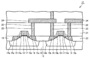
以下、この発明の実施の形態を、図面を参照して説明する。まず、この発明の一実施形態に係るプラズマ処理装置によって製造される半導体素子の構成について説明する。図1は、この発明の一実施形態に係るプラズマ処理装置によって製造されるMOS型半導体素子の一部を示す概略断面図である。なお、図1に示すMOS型半導体素子において、導電層をハッチングで示している。 Embodiments of the present invention will be described below with reference to the drawings. First, the configuration of a semiconductor element manufactured by a plasma processing apparatus according to an embodiment of the present invention will be described. FIG. 1 is a schematic sectional view showing a part of a MOS type semiconductor device manufactured by a plasma processing apparatus according to an embodiment of the present invention. In the MOS type semiconductor device shown in FIG. 1, the conductive layer is indicated by hatching.
図1を参照して、MOS型半導体素子11には、シリコン基板12上に、素子分離領域13、p型ウェル14a、n型ウェル14b、高濃度n型不純物拡散領域15a、高濃度p型不純物拡散領域15b、n型不純物拡散領域16a、p型不純物拡散領域16b、およびゲート酸化膜17が形成されている。ゲート酸化膜17を間に挟むように形成される高濃度n型不純物拡散領域15aおよび高濃度p型不純物拡散領域15bのいずれか一方は、ドレインとなり、他方はソースとなる。
Referring to FIG. 1, MOS
また、ゲート酸化膜17の上には、導電層となるゲート電極18が形成されており、ゲート電極18の側部には、絶縁膜となるゲート側壁部19が形成される。さらに、上記したゲート電極18等が形成されたシリコン基板12の上には、絶縁膜21が形成される。絶縁膜21には、高濃度n型不純物拡散領域15aおよび高濃度p型不純物拡散領域15bに連なるコンタクトホール22が形成され、コンタクトホール22内には穴埋め電極23が形成される。さらにその上に導電層となるメタル配線層24が形成される。さらに、絶縁層となる層間絶縁膜(図示せず)および導電層となるメタル配線層を交互に形成し、最後に外部との接点となるパッド(図示せず)を形成する。このようにMOS型半導体素子11が形成されている。
In addition, a
この発明に係るプラズマ処理装置によって製造される半導体素子には、後述するように、被処理基板上に成膜ガスを吸着させてプラズマ処理を行うことで形成されたシリコン酸化膜が、例えば、ゲート酸化膜17として含まれる。また、この発明に係るプラズマ処理装置によって成膜される絶縁膜は、上記したゲート酸化膜を構成するシリコン酸化膜であって、被処理基板上に成膜ガスを吸着させてプラズマ処理することにより成膜されている。
In a semiconductor element manufactured by the plasma processing apparatus according to the present invention, as will be described later, a silicon oxide film formed by adsorbing a film forming gas on a substrate to be processed and performing plasma processing, for example, a gate An
次に、この発明の一実施形態に係るプラズマ処理装置の構成および動作について説明する。 Next, the configuration and operation of the plasma processing apparatus according to one embodiment of the present invention will be described.
図2は、この発明の一実施形態に係るプラズマ処理装置の要部を示す概略断面図である。また、図3は、図2に示すプラズマ処理装置に含まれるスロットアンテナ板を下方側、すなわち、図2中の矢印IIIの方向から見た図である。なお、図2および後述する図8において、理解の容易の観点から、部材の一部のハッチングを省略している。また、図2および後述する図8中の二点鎖線で、処理容器内に発生させたプラズマを模式的に示している。 FIG. 2 is a schematic cross-sectional view showing the main part of the plasma processing apparatus according to one embodiment of the present invention. 3 is a view of the slot antenna plate included in the plasma processing apparatus shown in FIG. 2 as viewed from the lower side, that is, from the direction of arrow III in FIG. In FIG. 2 and FIG. 8 to be described later, some of the members are not hatched for easy understanding. Moreover, the plasma generated in the processing container is schematically shown by a two-dot chain line in FIG. 2 and FIG. 8 described later.
図2および図3を参照して、プラズマ処理装置31は、その内部で被処理基板Wにプラズマ処理を行う処理容器32と、処理容器32内にプラズマ処理用の反応ガスを供給するプラズマ処理用のガス供給部33と、その上に被処理基板Wを支持する円板状の支持台34と、処理容器32内にプラズマを発生させるプラズマ発生機構39と、成膜ガスやパージガスの供給を行うガス供給機構と、ガスの排気を行うガス排気機構と、プラズマ処理装置31全体を制御する制御部(図示せず)とを備える。制御部は、プラズマ処理用のガス供給部33におけるガス流量、処理容器32内の圧力等、プラズマ処理装置31全体の制御を行なう。
2 and 3, the
処理容器32は、支持台34の下方側に位置する底部41と、底部41の外周から上方向に延びる側壁42とを含む。側壁42は、一部を除いて略円筒状である。処理容器32の底部41には、その一部を貫通するように排気用の排気孔43が設けられている。処理容器32の上部側は開口しており、処理容器32の上部側に配置される蓋部44、後述する誘電体窓36、および誘電体窓36と蓋部44との間に介在するシール部材としてのOリング45によって、処理容器32は密封可能に構成されている。
The
プラズマ処理用のガス供給部33は、側壁42の上部側の一部において、処理容器32内にプラズマ処理用ガスを供給する複数のプラズマ処理用のガス供給孔46を設けることにより形成されている。複数のプラズマ処理用のガス供給孔46は、周方向に等配に設けられている。プラズマ処理用のガス供給部33には、反応ガス供給源(図示せず)からプラズマ処理用のガスが供給される。
The plasma processing
支持台34は、静電チャック(図示せず)によりその上に被処理基板Wを支持可能である。また、支持台34は、内部に設けられた温度調整機構(図示せず)により所望の温度に設定可能である。支持台34は、底部41の下方側から垂直上方に延びる絶縁性の筒状支持部49に支持されている。上記した排気孔43は、筒状支持部49の外周に沿って処理容器32の底部41の一部を貫通するように設けられている。環状の排気孔43の下方側には排気管(図示せず)を介して排気装置(図示せず)が接続されている。排気装置は、ターボ分子ポンプなどの真空ポンプを有している。排気装置により、処理容器32内を所定の圧力まで減圧することができる。
The
プラズマ発生機構39は、処理容器32外に設けられており、プラズマ励起用のマイクロ波を発生させるマイクロ波発生器35と、複数のスロット孔40が設けられており、誘電体窓36の上方側に配置され、マイクロ波を誘電体窓36に放射するスロットアンテナ板37と、スロットアンテナ板37の上方側に配置され、後述する同軸導波管54により導入されたマイクロ波を径方向に伝播する誘電体部材38とを含む。
The
マッチング機構51を有するマイクロ波発生器35は、モード変換器52および導波管53を介して、マイクロ波を導入する同軸導波管54の上部に接続されている。例えば、マイクロ波発生器35で発生させたTEモードのマイクロ波は、導波管53を通り、モード変換器52によりTEMモードへ変換され、同軸導波管54を伝播する。マイクロ波発生器35において発生させるマイクロ波の周波数としては、例えば、2.45GHzが選択される。
A
誘電体窓36は、略円板状であって、誘電体で構成されている。なお、誘電体窓36の具体的な材質としては、石英やアルミナ等が挙げられる。
The
スロットアンテナ板37は、薄板状であって、円板状である。複数の長孔状のスロット孔40については、図3に示すように、一対のスロット孔40が略ハの字状に直交するように設けられており、一対をなしたスロット孔40が周方向に所定の間隔を開けて設けられている。また、径方向においても、複数の一対のスロット孔40が所定の間隔を開けて設けられている。
The
マイクロ波発生器35により発生させたマイクロ波は、同軸導波管54を通って、誘電体部材38に伝播され、スロットアンテナ板37に設けられた複数のスロット孔40から誘電体窓36に放射される。誘電体窓36を透過したマイクロ波は、誘電体窓36の直下に電界を生じさせ、処理容器32内にプラズマを生成させる。すなわち、プラズマ処理装置31において処理に供されるマイクロ波プラズマは、上記した構成のスロットアンテナ板37および誘電体部材38を含むラジアルラインスロットアンテナ(RLSA:Radial Line Slot Antena)により生成されている。
Microwaves generated by the
図4は、プラズマ処理装置31においてプラズマを発生させた際の処理容器32内における誘電体窓36の下面48からの距離とプラズマの電子温度との関係を示すグラフである。図5は、プラズマ処理装置31においてプラズマを発生させた際の処理容器32内における誘電体窓36の下面48からの距離とプラズマの電子密度との関係を示すグラフである。
FIG. 4 is a graph showing the relationship between the distance from the
図4および図5を参照して、誘電体窓36の直下の領域、具体的には、一点鎖線で示すおおよそ10mm程度までの領域26は、いわゆるプラズマ生成領域と呼ばれる。この領域26においては、プラズマの電子温度が1.5〜2.5eV程度であって比較的高く、プラズマの電子密度が1×1012cm−3よりも大きい。一方、二点鎖線で示す10mmを越える領域27は、プラズマ拡散領域と呼ばれる。この領域27においては、プラズマの電子温度が1.0〜1.3eV程度、少なくとも1.5eVよりも低く、プラズマの電子密度が1×1012cm−3程度、少なくとも1×1011cm−3よりも高い。プラズマ処理装置31の処理容器32内においては、マイクロ波により励起され、このようなプラズマの状態となっている。そして、後述する被処理基板Wに対するプラズマ処理は、プラズマ拡散領域で行なわれる。すなわち、プラズマ処理工程は、被処理基板の表面近傍において、プラズマの電子温度が1.5eVよりも低く、かつプラズマの電子密度が1×1011cm−3よりも高いマイクロ波プラズマを用いた処理である。
Referring to FIGS. 4 and 5, the region immediately below
次に、この発明の一実施形態に係るプラズマ処理装置31に備えられるガス供給機構および遮断機構の構成について説明する。図6は、後述するヘッド部62の一部を、図2に示す矢印IIIの方向から見た図である。図7は、図6に示すヘッド部62の一部を示す断面図であり、図2中のVIIで示す部分の拡大断面図である。
Next, the configuration of the gas supply mechanism and the shutoff mechanism provided in the
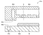
図2、図6および図7を参照して、ガス供給機構61は、円板状のヘッド部62と、処理容器32の側壁42側から延び、内方側部分である内方側端部65がヘッド部62に接続されてヘッド部62を支持する支持部66とを含む。
2, 6, and 7, the
ヘッド部62は、支持台34の上方側を覆って支持台34との間に小容積領域Sを形成可能な第一の位置および第一の位置と異なる第二の位置に移動可能である。小容積領域Sとは、処理容器32全体の大容積の領域と比較し、ヘッド部62と支持台34との間に形成される小さな容積の領域をいう。なお、第一および第二の位置については、後述する。
The
円板状のヘッド部62は、その外径側領域から板厚方向下方側に延びる環状の延出部67を備える。ヘッド部62は、被処理基板Wよりも大きく構成されている。そして、延出部67は、ヘッド部62において、板厚方向から見た場合に、支持台34上に支持された被処理基板Wよりも外径側に位置するように設けられている。上記した第一の位置とは、この場合、ヘッド部62が支持台34の上方側を覆う位置である。第一の位置においては、支持台34の外径側の上面47と延出部67を構成する下面63とが対向する。
The disc-shaped
ヘッド部62は、ヘッド部62が第一の位置、すなわち、支持台34上に配置された際に、支持台34上に支持された被処理基板Wに対向する位置に設けられ、成膜ガスやパージガスを供給する第一のガス供給孔68を含む。第一のガス供給孔68は、ヘッド部62の下方側に位置する面の一部を開口するように複数設けられている。複数の第一のガス供給孔68は、図6中縦方向および横方向に所定の間隔を開けて、それぞれ略等配に設けられている。なお、第一のガス供給孔68については、単一であってもよい。すなわち、第一のガス供給孔68については、ヘッド部62の下方側に位置する面の一部を開口するように単一で設けられていてもよい。
The
ヘッド部62の内部および支持部66の内部には、一方側が各第一のガス供給孔68に通じ、他方側が処理容器32外に設けられ、成膜ガスやパージガスを供給するガス供給部(図示せず)に通ずる第一のガス供給路69が設けられている。ガス供給機構61は、第一のガス供給路69および複数の第一のガス供給孔68を介して、処理容器32の外部側から被処理基板Wに対して、成膜ガスやパージガスを供給する。ヘッド部62は、小容積領域Sへのプラズマを遮蔽するために金属で構成されている。ヘッド部62の材質としては、具体的には、例えば、アルマイトやイットリア等により酸化皮膜が形成されたアルミニウムが好適に用いられる。
Inside the
処理容器32内の空間から小容積領域Sを遮断する遮断機構64は、支持台34上に支持された被処理基板Wの外方側に設けられたガス排気孔70および後述するガス排気路71を有し、ガスの排気を行うガス排気機構を含む。ガス排気孔70は、ヘッド部62のうち、延出部67の下面63に開口を有し、下面63から凹むように設けられている。ガス排気孔70は、環状に連なった形状である。すなわち、環状の延出部67の形状に沿って設けられている。
The
板厚方向から見た場合に延出部67が位置する部分であって、ヘッド部62の周縁における内部には、一方側がガス排気孔70に通じ、他方側が処理容器32外に設けられ、余剰の成膜ガス等を排気するガス排気部(図示せず)に通ずるガス排気路71が設けられている。ガス排気機構は、ガス排気路71および環状のガス排気孔70を介して、処理容器32の外部に、ガス供給機構61から供給された余剰の成膜ガス等を排気する。
When viewed from the thickness direction, the extending
また、遮断機構64は、支持台34上に支持された被処理基板Wの周縁に設けられ、パージガスを供給可能な第二のガス供給孔を有し、第二のガス供給孔からパージガスを供給するパージガス供給機構を含む。ここで、上記したガス排気孔70は、第二のガス供給孔を兼ねるものである。
The shut-off
ヘッド部62の周縁における内部には、一方側が第二のガス供給孔に通じ、他方側が処理容器32外に設けられ、パージガスを供給するパージガス供給部(図示せず)に通ずる第二のガス供給路が設けられている。ここで、上記したガス排気路71は、第二のガス供給路を兼ねるものである。すなわち、第二のガス供給路を兼ねるガス排気路71および第二のガス供給孔を兼ねるガス供給孔80を介して、処理容器32の外部側からパージガスを供給することができる。
Inside the peripheral edge of the
なお、遮断機構64は、ガス排気機構のみを備えていてもよく、パージガス供給機構のみを備えていてもよい。
The
また、プラズマ処理装置31に備えられる処理容器32には、側壁42の一部が外方側に延びるようにして形成されており、ヘッド部62を収容可能な収容部76が設けられている。収容部76は、側壁42の一部から外方側に向かって真直ぐ延びるようにして形成されている。なお、この収容部76内の領域が、図2に示すプラズマ処理装置31におけるヘッド部62が移動可能な第二の位置となる。
Further, the
上記したようにヘッド部62は、支持台34の上方側である第一の位置、および収容部76内である第二の位置に移動可能である。すなわち、ヘッド部62は、図2に示す矢印A1の方向またはその逆の方向に移動可能である。なお、ヘッド部62が第一の位置に配置された場合を図2で示し、ヘッド部62が第二の位置に配置された場合を、図8で示している。図8は、図2に示すプラズマ処理装置31において、ヘッド部62が収容部76に収容された状態を示す概略断面図である。
As described above, the
また、プラズマ処理装置31には、収容部76内の領域と収容部76外の領域、ここでは、処理容器32との領域を遮断する遮断機構としての遮蔽板77が設けられていてもよい。遮蔽板77は、側壁42の内壁面78に沿って、図2中の矢印A2の方向またはその逆の方向に移動可能である。遮蔽板77により、収容部76内の領域と収容部76外の領域を遮蔽した場合を、図8に示している。
Further, the
次に、図1〜図8、図9、図10、図11、および図12を用いて、絶縁膜を含む半導体素子を製造する方法について説明する。図9は、図2に示すプラズマ処理装置31を用いて、成膜ガス吸着工程において、被処理基板Wにガスを供給する際のシーケンスを概略的に示す図である。図9においては、ヘッド部62、被処理基板W、および支持台34を模式的に示している。図10は、処理の流れを示す簡単なチャート図である。図10においては、(A)から(H)に向かって時間が経過していくものである。なお、図10において、折れ線で示すチャートについては、上側に位置する場合、各ガスの供給状態またはプラズマの生成状態を示し、下側に位置する場合、各ガスの供給停止状態を示す。図11および図12は、ガス供給機構61等の一部を示す概略断面図である。図11は、アルゴンガスのみを第一のガス供給孔68から供給する場合を示す。図12は、アルゴンガスおよびプリカーサガスを混合した成膜ガスを第一のガス供給孔68から供給する場合を示す。図11および図12においては、理解の容易の観点から、第一のガス供給路69との接続部分については、概略的に示している。
Next, a method for manufacturing a semiconductor element including an insulating film will be described with reference to FIGS. 1 to 8, 9, 10, 11, and 12. FIG. 9 is a diagram schematically showing a sequence when gas is supplied to the substrate W to be processed in the film forming gas adsorption process using the
ここで、図11に示すガス供給機構61の構成について簡単に説明する。図11を参照して、ガス供給機構61は、アルゴンガスの供給系統55aと、プリカーサガスの供給系統55bとを備える。アルゴンガスの供給系統55aは、流量を調整するMFC(Mass Flow Controller)56aと、パイプ58aと、パイプ58aの間において、開閉によりアルゴンガスの供給および停止を行うバルブ57aとを備える。また、プリカーサガスの供給系統55bは、プリカーサガスの流量を調整するMFC56bと、パイプ58bと、各所において開閉によりプリカーサガスの供給および停止を行うバルブ57b、57c、57d、57eとを備える。バルブ57aの下流側のパイプとバルブ57cの下流側のパイプとは、共用されており、ヘッド部62内に設けられた第一のガス供給路69に連結されている。図12に示すガス供給機構61については、図11に示す符号と同じ符号を付して、その説明を省略する。なお、バルブ57a〜57eにおいて、ハッチングで示している状態のときは、閉じられている状態を示し、白抜きで示している状態のときは、開けられている状態を示す。
Here, the configuration of the
なお、後述するプラズマ処理時における支持台34の温度は、例えば、100〜600℃、好ましくは、300〜400℃の間の任意の温度が選択される。 In addition, the temperature of the support stand 34 at the time of the plasma processing mentioned later is 100-600 degreeC, for example, Preferably, arbitrary temperature between 300-400 degreeC is selected.
処理の開始(図10(A))後、すなわち、被処理基板Wを静電チャックにより支持させた後、まず、プラズマを発生させる。プラズマ発生の際には、処理容器32内にアルゴンガス、酸素ガスの供給を開始し、マイクロ波プラズマを生成する。ヘッド部62については、アルゴンガスの供給を開始する。具体的には、図11に示すように、バルブ57aを開ける。そうすると、ヘッド部62に設けられた第一のガス供給路69にアルゴンガスが供給される。ここで、被処理基板Wの上部側の領域においては、ヘッド部62に覆われた状態ではなく、プラズマに曝された状態であり、初期における処理の下地層となる被処理基板Wの上面の酸化処理が行われる(図10(B))。
After the start of processing (FIG. 10A), that is, after the substrate to be processed W is supported by the electrostatic chuck, plasma is first generated. When plasma is generated, supply of argon gas and oxygen gas into the
次に、ヘッド部62を第一の位置、すなわち、被処理基板Wがその上に支持された支持台34の上方側に移動させる(図10(C))。そして、支持台34とヘッド部62との間に小容積領域Sを形成する。その後、第一のガス供給孔68から、パージガスを被処理基板Wに向けて供給する(図9(K1)、図10(D))。この場合、パージガスとしてのアルゴンガスは、既に供給されている。また、ヘッド部62におけるガスの排気を行う。排気については、上記したガス排気機構を用いて行う。
Next, the
次に、成膜ガスを供給する(図9(K2)、図10(E))。具体的には、プリカーサガスを含む成膜ガスを複数の第一のガス供給孔68から噴出するようにして供給する。この場合、アルゴンガスの供給は連続しておいて、プリカーサガスを併せて供給するようにする。すなわち、図12に示すように、バルブ57aを開けたまま、バルブ57b、57cを開ける。そうすると、バルブ57aとバルブ57cの下流側において、アルゴンガスとプリカーサガスが混合され、ヘッド部62に設けられた第一のガス供給路69に供給される。この実施形態においては、成膜ガスは、アルゴンガスとプリカーサガスとの混合ガスであり、それぞれの流量については、アルゴンガスが500sccmであり、プリカーサガスが100sccmである。なお、プリカーサガスとしては、BTBAS(bis−tertiaryl−buthyl−amino−silane)を含むガスを用いている。また、ヘッド部62におけるガスの排気を行う。このガスの排気は、連続して行われていてもよい。
Next, a deposition gas is supplied (FIG. 9 (K 2 ), FIG. 10 (E)). Specifically, the film forming gas containing the precursor gas is supplied so as to be ejected from the plurality of first gas supply holes 68. In this case, the argon gas is continuously supplied, and the precursor gas is supplied together. That is, as shown in FIG. 12, the
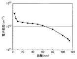
ここで、圧力について説明する。図13は、処理容器全体におけるガス流量と所定の圧力に到達するまでの到達時間との関係を示すグラフである。図14は、支持台34とヘッド部62との間に形成される小容積領域Sにおけるガス流量と所定の圧力に到達するまでの到達時間との関係を示すグラフである。図13および図14中、縦軸は、到達時間(秒)を示し、横軸は、ガス流量(sccm)を示す。なお、ガス流量は、Ar(アルゴン)ガス換算で示している。図13および図14に示すグラフは、1Torrから3Torrに昇圧する場合のグラフである。図13に示す場合において、処理容器32全体の容積は、約54リットルである。図14に示す場合において、支持台34とヘッド部62との間に形成される小容積領域Sの容積は、約0.75リットルである。なお、このような容積は、例えば、プラズマ処理装置31において処理する被処理基板Wの直径を300mmとした場合を想定している。
Here, the pressure will be described. FIG. 13 is a graph showing the relationship between the gas flow rate in the entire processing container and the arrival time until a predetermined pressure is reached. FIG. 14 is a graph showing the relationship between the gas flow rate in the small volume region S formed between the
図13および図14を参照して、いずれのガス流量においても、3Torrに到達するまでに要する時間は、図14に示す場合の方が、大幅に短くなっていることが把握できる。なお、支持台34とヘッド部62の間に形成される小容積領域Sの容積は、例えば、処理容器32の全体の容積の50%以内であることが好ましい。また、小容積領域Sの容積は、処理容器32の全体の容積の20%以内であればさらに好ましい。ここで、上記した図13および図14に示す場合であれば、小容積領域Sの容積は、処理容器32の全体の容積のおおよそ1.4%となる。
Referring to FIGS. 13 and 14, it can be understood that the time required to reach 3 Torr is significantly shorter in the case shown in FIG. 14 at any gas flow rate. In addition, it is preferable that the volume of the small volume area | region S formed between the
このようにして、第一のガス供給孔68から、成膜ガスを被処理基板Wに向けて供給する。そうすると、被処理基板W上にプリカーサガス分子がおおよそ1層化学吸着される。この場合、シリコン原子を含む分子層が化学吸着層としておおよそ1層程度形成される。ここで、化学吸着層の上には、過剰に供給された物理的なプリカーサガス分子の吸着の層、すなわち、過吸着の物理吸着層が形成される。
In this way, the deposition gas is supplied from the first
成膜ガスを被処理基板W上に化学吸着させた後、過吸着のプリカーサガスを含む成膜ガスを除去するための物理吸着層除去工程、および小容積領域S内のガスの置換を行うため、パージガスを供給する(図9(K3)、図10(F))。パージガスの供給に際しては、プリカーサガスの供給を停止し、ヘッド部62に設けられた第一のガス供給孔68からアルゴンガスの供給のみを行うことによりなされる。この実施形態においては、パージガスとして、アルゴンガスを500sccmの流量にて供給する。また、ヘッド部62におけるガスの排気を行う。このガスの排気は、連続して行われていてもよい。
In order to perform the physical adsorption layer removal step for removing the film forming gas containing the over-adsorbed precursor gas and the gas in the small volume region S after the film forming gas is chemically adsorbed on the substrate W to be processed. The purge gas is supplied (FIG. 9 (K 3 ), FIG. 10 (F)). When supplying the purge gas, the supply of the precursor gas is stopped and only the argon gas is supplied from the first
次に、パージガスを供給した後、マイクロ波による化学吸着層のプラズマ処理を行う。この実施形態においては、プラズマ処理用ガスは、アルゴン(Ar)ガスと酸素(O2)ガスとの混合ガスであり、それぞれの流量については、アルゴンガスが500sccmであり、酸素ガスが60sccmである。プラズマ処理に際しては、ヘッド部62を第2の位置となる収容部76に移動して収容後(図9(K4)、図10(G))、遮蔽板77を上方向に移動させ、収容部76内と収容部76外とを遮蔽板77により遮断する。その後、被処理基板Wを処理容器32内の誘電体窓36の直下に置く状態、すなわち、ヘッド部62によって覆われていない状態とし、被処理基板Wの上に形成されたシリコン原子を含む化学吸着層のマイクロ波によるプラズマ処理を行う(図10(H))。このとき、処理容器32内には、連続してプラズマが生成されている。この場合のマイクロ波によるプラズマ処理は、シリコン原子の酸化処理である。このプラズマ処理は、上記したプラズマ拡散領域で行う。
Next, after supplying the purge gas, plasma treatment of the chemical adsorption layer by microwave is performed. In this embodiment, the plasma processing gas is a mixed gas of argon (Ar) gas and oxygen (O 2 ) gas, and for each flow rate, argon gas is 500 sccm and oxygen gas is 60 sccm. . In the plasma processing, the
このようにして、原子層が一層程度形成された成膜を行う。そして、この一連の流れを、プラズマを発生させた状態のまま、所望の膜厚となるまで繰り返す。すなわち、図10における(C)から(H)までの工程を1サイクルとして、所望の膜厚となるまでサイクルを繰り返し行う。 In this way, film formation is performed in which about one atomic layer is formed. This series of flows is repeated until the desired film thickness is obtained while the plasma is generated. That is, the steps from (C) to (H) in FIG. 10 are defined as one cycle, and the cycle is repeated until a desired film thickness is obtained.
ここで、従来のプラズマ処理については、プラズマ生成の際、つまりプラズマ着火後にプラズマが安定するまでの時間を要するが、本実施形態のプラズマ処理については、プラズマを発生させた状態のままであるため、プラズマが安定するまでの時間を要しない。 Here, with respect to the conventional plasma processing, it takes time for the plasma to be stabilized at the time of plasma generation, that is, after the plasma is ignited. However, in the plasma processing of the present embodiment, the plasma is still generated. , No time is required until the plasma stabilizes.
これについて簡単に説明すると、以下の通りである。図15は、プラズマが安定するために要する時間を示すグラフであり、整合時間とチューナーポジションの変化を示したグラフである。図15中、縦軸は、基準の位置に対するチューナーの位置、いわゆるチューナーポジションを示し、横軸は、チューナーのポジションが整合するまでに要する整合時間、すなわち、経過時間(秒)を示す。チューナーは、図示はしないが、上記した図2等におけるマッチング機構51の内部に設けられているものであり、マイクロ波発生器35にて発生させたマイクロ波の波長をチューナーの先端の位置を上下させることにより調整し、安定したマイクロ波を供給するためのものである。図15中において、複数設けられるチューナーについて、第一のチューナーの位置を位置T1、第二のチューナーの位置を位置T2として示している。チューナーが上下方向に移動せず、その位置が安定したときが、安定してマイクロ波が供給されている状態であり、つまり、プラズマが安定していることとなる。
This will be briefly described as follows. FIG. 15 is a graph showing the time required for the plasma to stabilize, and is a graph showing changes in matching time and tuner position. In FIG. 15, the vertical axis indicates the tuner position relative to the reference position, that is, the so-called tuner position, and the horizontal axis indicates the alignment time required until the tuner position is aligned, that is, the elapsed time (seconds). Although not shown, the tuner is provided inside the
図15を参照して、位置T1および位置T2が確実に安定するのは、90秒経過後であり、少なくとも15秒程度までは、位置T1および位置T2が上下に激しく移動していることが分かる。この15秒以前にプラズマ処理を行うと、不安定なプラズマ状態で処理することになり、例えば、電子温度の高い活性種が被処理基板Wにプラズマダメージを与えるおそれがある。すなわち、プラズマの安定に要する時間は、少なくとも約15秒となり、この時間が経過するまで、プラズマの処理を待つ必要がある。このような待ち時間が、数十回〜数百回のサイクル毎に生じるとなると、スループットの大幅な低下を招くことになる。 Referring to FIG. 15, the positions T 1 and T 2 are surely stabilized after 90 seconds, and the positions T 1 and T 2 move violently up and down until at least about 15 seconds. I understand that. If the plasma treatment is performed before 15 seconds, the treatment is performed in an unstable plasma state. For example, active species having a high electron temperature may cause plasma damage to the substrate W to be processed. That is, the time required for plasma stabilization is at least about 15 seconds, and it is necessary to wait for plasma processing until this time elapses. If such a waiting time occurs every several tens to several hundreds of cycles, the throughput will be significantly reduced.
具体的には、例えば、上記した処理容器32と同様の容積において、直径が300mmの被処理基板に薄膜を形成する場合を考えると、ガス吸着工程については、1秒程度であるが、パージガスの供給による成膜ガスの排気に要する時間は20秒程度かかり、プラズマの安定に要する時間を含めたプラズマ処理に要する時間は60秒程度かかり、プラズマ処理用のガスの排気に要する時間は、20秒程度かかる。そうすると、1サイクルのサイクルタイムは、101秒かかることになる。原子層一層はおおよそ1Å(オングストローム)程度である。実際に成膜に要求される膜厚としては、膜厚1nm〜500nmが選択されるが、例えば、100Å(=10nm)の膜厚の層を形成しようとすると、100サイクル行う必要があり、100サイクル×101秒=10100秒=2.5時間半以上かかることとなってしまう。
Specifically, for example, in the case where a thin film is formed on a substrate to be processed having a diameter of 300 mm in the same volume as the
しかし、本願発明の構成によれば、プラズマを発生させた状態のままとすることができるので、このような待ち時間、具体的には、少なくとも上記した図15の場合の15秒程度のプラズマが安定するために要する時間が生じることはない。したがって、サイクルタイム、すなわち、上記した一連の流れに要する時間を大幅に短縮することができ、スループットの向上を図ることができる。 However, according to the configuration of the present invention, it is possible to keep the plasma generated, so that such a waiting time, specifically, at least about 15 seconds of plasma in the case of FIG. No time is required to stabilize. Therefore, the cycle time, that is, the time required for the above-described series of flows can be greatly shortened, and the throughput can be improved.
このようにして、被処理基板Wに対するシリコン酸化膜の成膜を行なう。その後、被処理基板Wに対して、所望の箇所のエッチング等を繰り返し、図1に示すような半導体素子を製造する。なお、このような処理を、RLSAを用いたPE−ALD処理という。また、このような装置を、RLSAを用いたPE−ALD装置ともいう。 In this manner, a silicon oxide film is formed on the substrate W to be processed. Thereafter, etching of a desired portion is repeated on the substrate W to be processed, and a semiconductor element as shown in FIG. 1 is manufactured. Such processing is referred to as PE-ALD processing using RLSA. Such an apparatus is also referred to as a PE-ALD apparatus using RLSA.
すなわち、このようなプラズマ処理装置31によると、ヘッド部62が第一の位置にある状態、すなわち、ヘッド部62が支持台34の上方側を覆い、支持台34とヘッド部62との間に小容積領域Sを形成し、処理容器32内の空間から小容積領域Sを遮断している状態において、成膜ガスの供給を行う。そうすると、成膜ガスの供給は処理容器32の空間よりも狭い領域であるため、成膜ガスの供給に要する時間の短縮を図ることができる。また、ヘッド部62が支持台34の上方側を覆うようにして小容積領域Sが形成されているため、成膜ガスを被処理基板Wに供給させている間も処理容器32内にプラズマを継続して発生させておくことができる。そうすると、成膜を行った後にヘッド部62を第二の位置に移動させて、そのままプラズマ処理を行うことができ、プラズマを発生させるために要する時間を省略することができる。したがって、プラズマ処理に要する時間を短縮することができる。また、この場合、処理容器32内の空間から小容積領域Sが遮断されており、プラズマ処理を行う際にも、処理容器32の内壁面が成膜ガスに曝されることがないため、処理容器32の内壁面への反応生成物の付着の抑制やパーティクル発生の抑制、処理容器32の内壁面のクリーニング工程数の減少を図ることができる。したがって、このようなプラズマ処理装置31によると、スループットの向上を図ることができると共に、高品質な膜を成膜することができる。
That is, according to such a
さらにこの場合、ヘッド部62を収容部76に収容し、遮蔽板77により遮蔽しているため、プラズマによる処理の際のヘッド部62および収容部76の内壁面へのプラズマ処理による反応生成物の付着等も低減することができる。
Further, in this case, since the
また、この場合、低電子温度のマイクロ波プラズマによりプラズマ処理を行っているため、成膜時におけるプラズマダメージを大きく低減することができる。したがって、このような成膜方法によると、高品質な膜を形成することができる。 In this case, since plasma processing is performed with microwave plasma having a low electron temperature, plasma damage during film formation can be greatly reduced. Therefore, according to such a film forming method, a high quality film can be formed.
ここで、上記の実施の形態においては、収容部は側壁の一部から外方側に向かって真直ぐ延びるようにして形成されることとしたが、これに限らず、収容部は、側壁の一部から外方側に向かって斜め方向に延びるようにして形成することにしてもよい。また、収容部の容積とヘッド部の大きさとをほぼ同一とし、ヘッド部の側壁において遮蔽機構を備えるよう構成してもよい。さらに遮蔽板の移動は上下方向に限らず、水平方向や円周方向、斜め方向に移動可能に構成してもよい。さらに、収容部内の空間と処理容器内の空間とを仕切るシャッター状のものを備えるようにしてもよい。さらに、遮蔽機構については、用途等に応じて設ける必要はない。 Here, in the above-described embodiment, the housing portion is formed so as to extend straight from a part of the side wall toward the outer side. You may decide to form it so that it may extend in the diagonal direction toward the outward side from a part. Further, the volume of the accommodating portion and the size of the head portion may be substantially the same, and a shielding mechanism may be provided on the side wall of the head portion. Furthermore, the movement of the shielding plate is not limited to the vertical direction, but may be configured to be movable in the horizontal direction, the circumferential direction, and the oblique direction. Furthermore, you may make it provide the shutter-shaped thing which partitions off the space in an accommodating part, and the space in a processing container. Furthermore, it is not necessary to provide a shielding mechanism according to the application.
なお、ヘッド部および支持部の温度を調整可能な温度調整機構を含むよう構成してもよい。こうすることにより、供給するガスの温度を適切にして、より効率的に成膜等を行うことができる。具体的には、例えば、ヒータおよびセンサ(いずれも図示せず)をヘッド部の内部および支持部の内部に設ける。そして、プラズマ処理装置に備えられる制御部により、センサからの温度情報に基づいて、ヒータのオンおよびオフを行うようにする。なお、ヒータやセンサは、ヘッド部や支持部の外側に取り付けるようにして設けることとしてもよい。また、いずれか一方、すなわち、ヘッド部のみや支持部のみに温度調整機構を備えるよう構成してもよい。 In addition, you may comprise so that the temperature adjustment mechanism which can adjust the temperature of a head part and a support part is included. By doing so, it is possible to perform film formation and the like more efficiently by adjusting the temperature of the supplied gas. Specifically, for example, a heater and a sensor (both not shown) are provided inside the head portion and inside the support portion. The heater is turned on and off based on the temperature information from the sensor by the control unit provided in the plasma processing apparatus. The heater and the sensor may be provided so as to be attached to the outside of the head part or the support part. Moreover, you may comprise so that either one, ie, only a head part or a support part, may be equipped with a temperature adjustment mechanism.
ここで、温度調整を行う際の設定温度については、用いるプリカーサガスによって任意に設定される。制御においては、例えば、用いるプリカーサガスの蒸気圧に対応する温度範囲に設定してもよい。なお、上記の実施の形態においては、第二のガス供給孔を兼ねるガス排気孔を環状となるように設けることとしたが、これに限らず、丸孔状のものや長孔状のものを複数周方向に間隔を空けて設けるように構成してもよい。 Here, the set temperature at the time of temperature adjustment is arbitrarily set depending on the precursor gas used. In the control, for example, a temperature range corresponding to the vapor pressure of the precursor gas to be used may be set. In the above-described embodiment, the gas exhaust hole that also serves as the second gas supply hole is provided so as to be annular. However, the present invention is not limited to this, and a round hole or a long hole is used. You may comprise so that it may provide in multiple circumferential directions at intervals.
また、上記の実施の形態においては、ガス排気機構による排気を連続して行うこととしたが、これに限らず、各工程において適宜タイミングを合わせてガス排気機構による排気を行うこととしてもよい。 In the above-described embodiment, exhaust by the gas exhaust mechanism is continuously performed. However, the present invention is not limited to this, and exhaust by the gas exhaust mechanism may be performed at an appropriate timing in each step.
これについて説明すると、以下の通りである。再び図9を参照して、ヘッド部62を第一の位置へ移動させた後、上記と同様に、パージガス、すなわち、ここではアルゴンガスの供給を開始する(図9(M1))。この時、同時にガス排気機構による排気を行わないようにする。そして、パージガスの供給をしている段階で、すなわち、パージガスの供給が終了する前に、ガス排気機構によるガスの排気を開始する(図9(L1))。そして、ガスの排気を行いながら、パージガスの供給を終了する(図9(L2))。その後、ガスの排気を停止し、次に成膜ガスの供給を開始する(図9(L3))。すなわち、アルゴンガスとプリカーサガスとの混合ガスを同時に供給し始める。次に、成膜ガスの供給をしている段階で、ガス排気機構によるガスの排気を開始する(図9(L4))。そして、ガスの排気を行いながら、成膜ガスの供給を終了する(図9(L5))。その後、再びガスの排気を停止し、再びパージガスの供給を開始する(図9(L6))。そして、パージガスの供給をしている段階で、すなわち、パージガスの供給が終了する前に、ガス排気機構によるガスの排気を開始する(図9(L7))。そして、ガスの排気を行いながら、パージガスの供給を終了する(図9(L8))。そして、最後に、ヘッド部62を第二の位置に移動させて(図9(M7))、プラズマ処理を行う。このように構成することにより、ガスの置換効率を改善することができる。
This will be described as follows. Referring to FIG. 9 again, after the
また、パージガスおよび成膜ガスの供給と、ガスの排気については、それぞれのタイミングが重ならないように行っていてもよい。再び図9を参照して、ヘッド部62を第一の位置に移動させた後、パージガスを供給する(図9(M1))。ここで、ガス排気機構による排気を行わない。その後、パージガスの供給を停止し、ガス排気機構による排気を開始する(図9(M2))。次に、ガス排気機構による排気を停止した後、成膜ガスの供給を開始する(図9(M3))。その後、成膜ガスの供給を停止し、ガス排気機構による排気を再び開始する(図9(M4))。次に、再びガス排気機構による排気を停止した後、パージガスの供給を開始する(図9(M5))。その後、パージガスの供給を再び停止し、ガス排気機構による排気を再び開始する(図9(M6))。その後、ヘッド部62を第二の位置に移動させて(図9(M7))、プラズマ処理を行う。このように構成することにより、ガスの置換効率を改善することができる。
Further, the supply of the purge gas and the film forming gas and the exhaust of the gas may be performed so that the respective timings do not overlap. Referring again to FIG. 9, after moving the
なお、支持台上に支持された被処理基板の外周側に、フォーカスリングを設けることにしてもよい。図16は、この場合におけるこの発明のさらに他の実施形態に係るプラズマ処理装置81aに備えられるヘッド部82aおよび支持台83aのうちの一部を拡大して示す拡大断面図であり、図7に示す断面に相当する。図16を参照して、ヘッド部82aには、第二のガス供給孔を兼ねるガス排気孔84aおよび第二のガス供給路を兼ねるガス排気路85aが設けられている。支持台83a上に支持された被処理基板Wの外周側には、環状であって、板状のフォーカスリング88aが設けられている。フォーカスリング88aは、所定の板厚を有し、ヘッド部82aに設けられたガス排気孔84aに対向する位置に設けられている。具体的には、フォーカスリング88aの上側に位置する一方の面が、ヘッド部82aの外周側に設けられた延出部の下方側に位置する面と対向するようにして設けられている。このように構成することにより、処理容器内の空間からの小容積領域S、すなわち、ヘッド部82aが第一の位置に配置された際のヘッド部82aと支持台83aとの間に形成される領域を遮断する効率を高めることができる。また、このようなフォーカスリング88aは、取り外し可能に設置されている。そのため、例え、成膜ガスがプラズマ中の反応種に曝されることによって生成された反応生成物が付着したとしても、交換や変更が容易である。したがって、メンテナンス性を向上させることができる。なお、このようなフォーカスリング88aは、被処理基板Wの処理における均一性向上にも効果的である。
In addition, you may decide to provide a focus ring in the outer peripheral side of the to-be-processed substrate supported on the support stand. FIG. 16 is an enlarged cross-sectional view showing a part of the
また、上記した第二のガス供給孔を兼ねるガス排気孔は、複数設けることにしてもよい。図17は、この場合におけるこの発明のさらに他の実施形態に係るプラズマ処理装置81bに備えられるヘッド部82bおよび支持台83bのうちの一部を拡大して示す拡大断面図であり、図7に示す断面に相当する。
A plurality of gas exhaust holes that also serve as the second gas supply holes may be provided. FIG. 17 is an enlarged cross-sectional view showing a part of a head part 82b and a
図17を参照して、ヘッド部82bには、第一のガス排気孔84b、第一のガス排気孔84bに通ずる第一のガス排気路85b、第二のガス排気孔86bおよび第二のガス排気孔86bに通ずる第二のガス排気路87bが設けられている。第一のガス排気孔84bは、第二のガス排気孔86bよりも、外径側に設けられている。また、第一のガス排気路85bについても、第二のガス排気路87bよりも、外径側に設けられている。このように構成することにより、第一のガス排気孔84bから成膜ガスを効果的に排気することができ、第二のガス排気孔86bからヘッド部62内部の小容積領域S内に侵入するプラズマ中の反応種を効果的に排気することができる。よって、それぞれの排気路内にて意図せずに形成される反応生成物を減少させることができる。また、ガスの排気効率を向上させて、小容積領域Sを遮断する効率を高めることができる。
Referring to FIG. 17, the head portion 82b includes a first gas exhaust hole 84b, a first
また、ガス排気孔と第二のガス供給孔とを別に設けるようにしてもよい。図18は、この場合におけるこの発明のさらに他の実施形態に係るプラズマ処理装置81cに備えられるヘッド部82cおよび支持台83cのうちの一部を拡大して示す拡大断面図であり、それぞれ図7に示す断面に相当する。
Moreover, you may make it provide a gas exhaust hole and a 2nd gas supply hole separately. FIG. 18 is an enlarged cross-sectional view showing a part of a
図18を参照して、ガス排気機構72は、支持台83c上に支持された被処理基板Wの外方側に設けられたガス排気孔84cを有する。ガス排気孔84cは、ヘッド部82cのうち、延出部73の下面74に開口を有し、下面74から凹むように設けられている。ガス排気孔84cは、環状に連なった形状である。すなわち、環状の延出部73の形状に沿って設けられている。
Referring to FIG. 18, the
板厚方向から見た場合に延出部73が位置する部分であって、ヘッド部82cの周縁における内部には、一方側がガス排気孔84cに通じ、他方側が処理容器外に設けられ、余剰の成膜ガス等を排気するガス排気部(図示せず)に通ずるガス排気路85cが設けられている。ガス排気機構72は、ガス排気路85cおよび環状のガス排気孔84cを介して、処理容器の外部に、成膜ガス等を排気する。
When viewed from the plate thickness direction, the
また、プラズマ処理装置81cに含まれ、パージガスを供給するパージガス供給機構75は、支持台83c上に支持された被処理基板Wの周縁となるヘッド部82cの周縁に設けられた第二のガス供給孔86cを備える。第二のガス供給孔86cは、ヘッド部82cのうち、延出部73の下面74に開口を有し、下面74から凹むように設けられている。第二のガス供給孔86cは、環状に連なった形状である。すなわち、環状の延出部73の形状に沿って設けられている。
A purge
ヘッド部82cの周縁における内部には、一方側が第二のガス供給孔86cに通じ、他方側が処理容器外に設けられ、パージガスを供給するパージガス供給部(図示せず)に通ずる第二のガス供給路87cが設けられている。第二のガス供給路87cおよび環状の第二のガス供給孔86cを介して、処理容器の外部側からパージガスを供給することができる。
Inside the peripheral edge of the
ヘッド部82cの周縁において、第二のガス供給孔86cは、ガス排気孔84cよりも外方側に設けられている。すなわち、円板状のヘッド部82cの径方向において、ガス排気孔84cが設けられた位置の方が、第二のガス供給孔86cが設けられた位置よりも、支持台83c上に支持された被処理基板Wに近くなるように構成されている。このように構成することにしてもよい。こうすることにより、より小容積領域Sの遮断効率を向上させることができる。具体的には、より外径側の部分においてパージガスを供給して、小容積領域S内へのプラズマの侵入等を効率的に排除し、より内径側の部分において、外径側で供給されたパージガスを含めた余剰な成膜ガスを効率的に排気して、小容積領域S外への成膜ガス等の拡散を抑制することができる。
At the periphery of the
図18に示すプラズマ処理装置において、処理の流れを説明する。図19は、図18に示すプラズマ処理装置81cを用いて、成膜ガス吸着工程において、被処理基板Wにガスを供給する際のシーケンスを概略的に示す図であり、図9に相当する。また、図9と同様に、図19においては、ヘッド部82c、被処理基板W、および支持台83cを模式的に示している。
The flow of processing in the plasma processing apparatus shown in FIG. 18 will be described. FIG. 19 is a diagram schematically showing a sequence when gas is supplied to the substrate W to be processed in the film forming gas adsorption process using the
処理の開始後、すなわち、被処理基板Wを静電チャックにより支持させた後、まず、プラズマを発生させる。プラズマ発生の際には、処理容器内にアルゴンガス、酸素ガスの供給を開始し、マイクロ波プラズマを生成する。ヘッド部82cについては、アルゴンガスの供給を開始する。さらに、第二のガス供給孔86cによるパージガスの供給を行う。このパージガスの供給は、連続して行われる。ここで、初期における処理の下地層となる被処理基板Wの上面の酸化処理が行なわれる。
After the processing is started, that is, after the substrate to be processed W is supported by the electrostatic chuck, first, plasma is generated. When plasma is generated, supply of argon gas and oxygen gas into the processing container is started to generate microwave plasma. About the
次に、ヘッド部82cを第一の位置、すなわち、被処理基板Wがその上に支持された支持台34の上方側に移動させる。そして、支持台83cとヘッド部82cとの間に小容積領域Sを形成する。その後、第一のガス供給孔79から、パージガスを被処理基板Wに向けて供給する(図19(N1))。この場合、パージガスとしてのアルゴンガスは、既に供給されている。また、ヘッド部82cにおけるガスの排気を行う。排気については、上記したガス排気機構を用いて行う。
Next, the
次に、成膜ガスを供給する(図19(N2))。具体的には、プリカーサガスを含む成膜ガスを複数の第一のガス供給孔79から噴出するようにして供給する。この場合、アルゴンガスの供給は連続しておいて、プリカーサガスを併せて供給するようにする。また、ヘッド部82cにおけるガスの排気を行う。このガスの排気は、連続して行われる。
Next, a deposition gas is supplied (FIG. 19 (N 2 )). Specifically, the film forming gas containing the precursor gas is supplied so as to be ejected from the plurality of first gas supply holes 79. In this case, the argon gas is continuously supplied, and the precursor gas is supplied together. Further, gas is exhausted from the
このようにして、第一のガス供給孔79から、成膜ガスを被処理基板Wに向けて供給する。そうすると、被処理基板W上にプリカーサガス分子がおおよそ1層化学吸着される。この場合、シリコン原子を含む分子層が化学吸着層としておおよそ1層程度形成される。
In this way, the deposition gas is supplied from the first
成膜ガスを被処理基板W上に化学吸着させた後、過吸着のプリカーサガスを含む成膜ガスを除去するための物理吸着層除去工程、および小容積領域S内のガスの置換を行うため、再びパージガスを供給する(図19(N3))。パージガスの供給に際しては、プリカーサガスの供給を停止し、ヘッド部82cに設けられた第一のガス供給孔79からアルゴンガスの供給のみを行うことによりなされる。また、ヘッド部82cにおけるガスの排気を行う。このガスの排気は、連続して行われる。
In order to perform the physical adsorption layer removal step for removing the film forming gas containing the over-adsorbed precursor gas and the gas in the small volume region S after the film forming gas is chemically adsorbed on the substrate W to be processed. Then, the purge gas is supplied again (FIG. 19 (N 3 )). When supplying the purge gas, the supply of the precursor gas is stopped and only the argon gas is supplied from the first
次に、パージガスを供給した後、マイクロ波による化学吸着層のプラズマ処理を行う。プラズマ処理に際しては、ヘッド部82cを第2の位置となる収容部76に移動して収容後(図19(N4))、遮蔽板77を上方向に移動させ、収容部76内と収容部76外とを遮蔽板77により遮断する。その後、被処理基板Wを処理容器32内の誘電体窓36の直下に置く状態、すなわち、ヘッド部82cによって覆われていない状態とし、被処理基板Wの上に形成されたシリコン原子を含む化学吸着層のマイクロ波によるプラズマ処理を行う。このとき、処理容器32内には、連続してプラズマが生成されている。
Next, after supplying the purge gas, plasma treatment of the chemical adsorption layer by microwave is performed. In the plasma processing, the
このようにして、原子層が一層程度形成された成膜を行う。そして、この一連の流れを、プラズマを発生させた状態のまま、所望の膜厚となるまで繰り返す。このように構成してもよい。 In this way, film formation is performed in which about one atomic layer is formed. This series of flows is repeated until the desired film thickness is obtained while the plasma is generated. You may comprise in this way.
また、上記の実施の形態においては、ガス排気機構による排気を連続して行うこととしたが、これに限らず、適宜タイミングを合わせてガス排気機構による排気を行うこととしてもよい。 In the above-described embodiment, exhaust by the gas exhaust mechanism is continuously performed. However, the present invention is not limited to this, and exhaust by the gas exhaust mechanism may be performed at an appropriate timing.
これについて説明すると、以下の通りである。再び図19を参照して、ヘッド部82cを第一の位置へ移動させた後、第二のガス供給孔86cから連続してパージガスの供給を行いながら、第一のガス供給孔79からパージガス、すなわち、ここではアルゴンガスの供給を開始する(図19(Q1))。この時、同時にガス排気機構による排気を行わないようにする。そして、第一のガス供給孔79からのパージガスの供給をしている段階で、すなわち、第一のガス供給孔79からのパージガスの供給が終了する前に、ガス排気機構によるガスの排気を開始する(図19(P1))。そして、ガスの排気を行いながら、第一のガス供給孔79からのパージガスの供給を終了する(図19(P2))。その後、ガスの排気を停止し、次に第一のガス供給孔79からの成膜ガスの供給を開始する(図19(P3))。すなわち、アルゴンガスとプリカーサガスとの混合ガスを同時に供給し始める。次に、成膜ガスの供給をしている段階で、ガス排気機構によるガスの排気を開始する(図19(P4))。そして、ガスの排気を行いながら、第一のガス供給孔79からの成膜ガスの供給を終了する(図19(P5))。その後、再びガスの排気を停止し、再び第一のガス供給孔79からのパージガスの供給を開始する(図19(P6))。そして、第一のガス供給孔79からのパージガスの供給をしている段階で、すなわち、第一のガス供給孔79からのパージガスの供給が終了する前に、ガス排気機構によるガスの排気を開始する(図19(P7))。そして、ガスの排気を行いながら、第一のガス供給孔79からのパージガスの供給を終了する(図19(P8))。そして、最後に、ヘッド部62を第二の位置に移動させて(図19(Q7))、プラズマ処理を行う。このように構成することにより、ガスの置換効率を改善することができる。
This will be described as follows. Referring to FIG. 19 again, after the
また、第一のガス供給孔79からのパージガスおよび成膜ガスの供給と、ガスの排気については、それぞれのタイミングが重ならないように行っていてもよい。再び図19を参照して、ヘッド部62を第一の位置に移動させた後、第二のガス供給孔86cから連続してパージガスの供給を行いながら、第一のガス供給孔79からのパージガスを供給する(図19(Q1))。ここで、ガス排気機構による排気を行わない。その後、第一のガス供給孔79からのパージガスの供給を停止し、ガス排気機構による排気を開始する(図19(Q2))。次に、ガス排気機構による排気を停止した後、第一のガス供給孔79からの成膜ガスの供給を開始する(図19(Q3))。その後、第一のガス供給孔79からの成膜ガスの供給を停止し、ガス排気機構による排気を再び開始する(図19(Q4))。次に、再びガス排気機構による排気を停止した後、第一のガス供給孔79からのパージガスの供給を開始する(図19(Q5))。その後、第一のガス供給孔79からのパージガスの供給を再び停止し、ガス排気機構による排気を再び開始する(図19(Q6))。その後、ヘッド部62を第二の位置に移動させて(図19(Q7))、プラズマ処理を行う。このように構成することにより、ガスの置換効率を改善することができる。
Further, the supply of the purge gas and the film forming gas from the first
なお、上記の実施の形態においては、ガス排気孔および第二のガス供給孔をそれぞれ共に、ヘッド部に設けることとしたが、これに限らない。図20は、この発明のさらに他の実施形態に係るプラズマ処理装置81dに備えられるヘッド部82dおよび支持台83dのうちの一部を拡大して示す拡大断面図である。図21は、この発明のさらに他の実施形態に係るプラズマ処理装置81eに備えられるヘッド部82eおよび支持台83eのうちの一部を拡大して示す拡大断面図である。図22は、この発明のさらに他の実施形態に係るプラズマ処理装置81fに備えられるヘッド部82fおよび支持台83fのうちの一部を拡大して示す拡大断面図である。図20〜図22は、それぞれ図7に示す断面に相当する。
In the above embodiment, both the gas exhaust hole and the second gas supply hole are provided in the head portion, but the present invention is not limited to this. FIG. 20 is an enlarged cross-sectional view showing a part of a
図20に示すプラズマ処理装置81dのように、ガス排気孔84dおよびガス排気路85dが、ヘッド部82dに設けられており、第二のガス供給孔86dおよび第二のガス供給路87dが、支持台83dに設けられている構成としてもよい。また、図21に示すプラズマ処理装置81eのように、ガス排気孔84eおよびガス排気路85eが、支持台83eに設けられており、第二のガス供給孔86eおよび第二のガス供給路87eが、ヘッド部82eに設けられている構成としてもよい。また、図22に示すプラズマ処理装置81fのように、ガス排気孔84f、ガス排気路85f、第二のガス供給孔86fおよび第二のガス供給路87fがそれぞれ共に、支持台83fに設けられている構成としてもよい。図20、図21、および図22のように構成すると、ヘッド部82d等の構造を簡略化することができる。
As in the
また、パージガス供給機構は、小容積領域から外れるようにパージガスを供給するよう構成してもよい。この場合の具体的な一例として、第二のガス供給孔を設ける際には、ガス排気孔と第二のガス供給孔とのなす角度を、鋭角とするようにしてもよい。図23は、この場合におけるこの発明のさらに他の実施形態に係るプラズマ処理装置81gに備えられるヘッド部82gおよび支持台83gのうちの一部を拡大して示す拡大断面図であり、図7に示す断面に相当する。
The purge gas supply mechanism may be configured to supply the purge gas so as to be out of the small volume region. As a specific example in this case, when the second gas supply hole is provided, the angle formed by the gas exhaust hole and the second gas supply hole may be an acute angle. FIG. 23 is an enlarged cross-sectional view showing a part of a
図23を参照して、プラズマ処理装置81gには、ヘッド部82gの周縁において、ガス排気孔84gが、真下方向に向かって開口している。そして、第二のガス供給孔86gは、真下方向ではなく、外方側に向かって所定の角度傾けて開口するように設けられている。ここでいう角度θは、第二のガス供給孔86gを構成する内径側の壁面88gとガス排気孔84gを構成する外径側の壁面89gとのなす角度をいい、この角度が鋭角となるという意味である。このように構成することにより、パージガスが、被処理基板Wの位置する側と反対の側に供給されることになるため、より効率よく小容積領域S内へのプラズマ等の侵入を抑制することができる。
Referring to FIG. 23, in the
また、支持台にガス排気孔や第二のガス供給孔を設ける際には、支持台の外周側に配置される別部材を設け、この別部材に対して、ガス排気孔や第二のガス供給孔を設けることにしてもよい。図24は、この場合におけるこの発明のさらに他の実施形態に係るプラズマ処理装置81hに備えられるヘッド部82hおよび支持台83hのうちの一部を拡大して示す拡大断面図であり、図7に示す断面に相当する。
Further, when providing the gas exhaust hole or the second gas supply hole in the support base, another member disposed on the outer peripheral side of the support base is provided, and the gas exhaust hole or the second gas supply is provided to the separate member. A supply hole may be provided. FIG. 24 is an enlarged cross-sectional view showing a part of the
図24を参照して、支持台83hの外周側には、支持台83hと別部材であるパージガス供給部材としての支持台外方部材88hが設けられている。支持台外方部材88hは、環状であって、支持台83hの外周面89hと支持台外方部材88hの内周面90hとが互いに対向して当接するように設けられている。ここで、ヘッド部82hには、ガス排気孔84hおよびガス排気路85hが設けられており、支持台外方部材88hには、第二のガス供給孔86hおよび第二のガス供給路87hが設けられている。
Referring to FIG. 24, a support base
このように構成することにより、従来の構造の支持台83hを用いながらパージガスを効率的に供給することができる。さらに、支持台83hにおける温度管理と支持台外方部材88hにおける温度管理を別途制御して、より適切な温度で、パージガスを供給することができる。また、支持台外方部材88hのみの交換や形状変更等が容易になる。
By comprising in this way, purge gas can be supplied efficiently, using the support stand 83h of the conventional structure. Further, it is possible to supply the purge gas at a more appropriate temperature by separately controlling the temperature management in the
なお、この場合において、支持台外方部材にガス排気孔およびガス排気路を設けることにしてもよいし、ガス排気孔、ガス排気路、第二のガス供給孔、第二のガス供給路を設けることにしてもよい。さらに、支持台と支持台外方部材とを着脱可能とするようにしてもよいし、支持台と支持台外方部材との間に、すき間を設けることにしてもよい。さらに、上下方向に位置する部材の全ての組合せについて、別部材で構成することにしてもよい。 In this case, the support base outer member may be provided with a gas exhaust hole and a gas exhaust path, or the gas exhaust hole, the gas exhaust path, the second gas supply hole, and the second gas supply path may be provided. It may be provided. Furthermore, the support base and the support base outer member may be detachable, or a gap may be provided between the support base and the support base outer member. Furthermore, you may decide to comprise by another member about all the combinations of the member located in an up-down direction.
なお、上記の実施の形態においては、ヘッド部は、処理容器内を横方向、すなわち、水平方向に進退するように移動することとしたが、これに限らず、ヘッド部は、処理容器内において、上下方向に移動可能なように構成することとしてもよい。 In the above embodiment, the head portion moves in the processing container so as to advance and retreat in the horizontal direction, that is, in the horizontal direction. However, the present invention is not limited to this. Further, it may be configured to be movable in the vertical direction.
図25は、この場合におけるプラズマ処理装置の一部を示す概略断面図である。図25を参照して、プラズマ処理装置91の処理容器92内には、ヘッド部93と支持部94とが備えられている。支持部94の外径側端部95は、処理容器92の内壁面96に取り付けられている。ヘッド部93および支持部94は、外径側端部95を回転中心として、図25中の矢印Cで示す方向、すなわち、上下方向に回転可能に構成されている。ヘッド部93は、第一の位置として、支持台97の上方側に配置される。また、ヘッド部93は、第二の位置として、図25に示す状態から、上側に回転させた状態に配置される。
FIG. 25 is a schematic sectional view showing a part of the plasma processing apparatus in this case. Referring to FIG. 25, a
成膜処理については、まず、ガスを吸着する工程において、ヘッド部93を支持台97の上方側に位置させる。そして、プラズマ処理時においては、図25中の矢印Cで示す方向に支持部94ごと回転させて、ヘッド部93を第二の位置、ここでは、内壁面96側に傾けた位置にする。そして、マイクロ波による被処理基板Wのプラズマ処理を行う。このように構成することにしてもよい。
Regarding the film forming process, first, in the step of adsorbing gas, the
ここで、図26に示すように、プラズマ処理装置111に備えられるヘッド部112は、支持部113の根元部114を回転中心として、矢印Dで示す方向に処理容器115内を水平方向に回転可能な構成としてもよい。また、プラズマ処理装置116に備えられるヘッド部117は、図27に示すように、支持部118ごと処理容器119内を矢印Eで示す水平方向に移動可能な構成としてもよい。
Here, as shown in FIG. 26, the
ここで、支持部113の構成については、以下のようにしてもよい。図28、図29、および図30は、図26に示す支持部113のうちの根元部114付近の構成を示す概略断面図である。図28に示す断面は、支持部113のうちの根元部114付近を、図26における紙面表裏方向に延びる面で切断した場合の断面に相当し、図29に示す断面は、図28に示す断面を90度回転させた場合の断面に相当し、図30に示す断面は、図29中のXXX−XXX断面に相当する。
Here, the configuration of the
図26、図28〜図30を参照して、支持部113のうちの根元部114には、回転可能な可動部151と、ベース153に固定されている固定部152とが設けられている。固定部152については、下方側に位置する部分が、土台となるベース153に取り付けられ、固定されている。一方、可動部151については、図28および図29に一点鎖線で示す紙面上下方向に延びる回転中心軸154を中心に、図26および図30中の矢印Dで示す方向におおよそ90度回転することができる。
Referring to FIGS. 26 and 28 to 30, the
支持部113および根元部114の内部においては、ヘッド部側にガスを供給するガス供給孔(図示せず)に通じるガス供給路155と、排気する成膜ガスの通路となり、ガス排気孔(図示せず)に通じるガス排気路156とが設けられている。ここで、ガス供給路155とガス排気路156とは、ガス供給路155が内側に位置し、ガス排気路156が外側に位置するよう、支持部113内において、二重に設けられている。すなわち、図29中の矢印H1で示す方向にガスが供給され、図30中の矢印H2で示す方向にガスが排気される。
Inside the
このように構成することにより、ガス供給路155から供給されるガスがガス供給路155の一部から漏洩したとしても、ガス排気路156が外側に設けられているため、ガス排気路156に漏洩したガスが入り込み、排気されることになる。そうすると、ガス供給路155から漏洩したガスが、他の部分に漏洩することはない。したがって、より安全かつ確実にガス供給路155からのガスをヘッド部に供給することができる。
With this configuration, even if the gas supplied from the
もちろん、上記した図28に示す場合において、ガス供給路155が二重以上の多重に設けられていてもよいし、ガス排気路156が二重以上の多重に設けられていてもよい。すなわち、ガス供給機構は、側壁側から延び、内方側部分がヘッド部に連結され、ヘッド部を支持する支持部を含む構成であり、排気機構は、支持部の内部に、排気された排気ガスの通路となる排気路を含み、ガス供給機構は、支持部の内部に、供給するガスの通路となるガス供給路を含み、ガス供給路は、ガス排気路の内側となるように多重に設けられていればよい。
Of course, in the case shown in FIG. 28 described above, the
また、上記したプラズマ処理装置において、排気系統を2つとすると、装置のメンテナンスの観点からも有利である。 In the plasma processing apparatus described above, if there are two exhaust systems, it is advantageous from the viewpoint of maintenance of the apparatus.
これについて説明すると、以下の通りである。図31は、この場合のプラズマ処理装置の一部を示す概略断面図であり、図2に相当する。図31に示すプラズマ処理装置81jにおいて、図2に示すプラズマ処理装置31と同様の構成については、同一の符号を付してその説明を省略する。図31を参照して、プラズマ処理装置81jは、処理容器32内の空間のガスを排気する排気孔43を有する第一の排気系統82jと、小容積領域S内のガスを排気するガス排気路に繋がる第二の排気系統83jとを有する。すなわち、プラズマ処理装置81jは、排気孔43からの第一の排気系統82jと、ガス排気孔70からの第二の排気系統83jという2つ独立した排気系統を備える構成である。具体的には、第一の排気系統82jを構成するドライポンプ84jや概略図示した配管85jと、第二の排気系統83jを構成するドライポンプ86jや概略図示した配管87jとが、それぞれ別個に設けられているものである。そして、それぞれの排気系統82j、83jが、燃焼により反応生成物や成膜ガス等を除害する除害装置88jに繋がっている。除害装置88jからの排気については、プラズマ処理装置81jが備えられている工場の排気設備へ送られる。
This will be described as follows. FIG. 31 is a schematic sectional view showing a part of the plasma processing apparatus in this case, and corresponds to FIG. In the
次に、排気系統が一つのプラズマ処理装置において、上記した処理を行った場合の排気について説明する。図32は、排気系統が一つのプラズマ処理装置における排気の流れを示す図である。排気系統が一つとは、処理容器の空間を排気する排気系統のみを有する構成である。図32を参照して、例えば、成膜ガスを供給する場合において、処理容器からの排気については成膜ガスが排気される(R1)。排気された成膜ガスの大部分は、コールドトラップ、すなわち、トラップ部分を低温にした機構にて、余剰の成膜ガスが捕集される。そして、ドライポンプを用いて排気され、除害装置にて成膜ガスを燃焼させて除害する。ここで、ドライポンプ内での成膜ガスの付着を防止するため、ドライポンプには、加熱したN2ガスが供給されている。次に、供給されたパージガスが排気され、コールドトラップで捕集され、燃焼させて除害される(R2)。次のプラズマ処理工程においては、排気系統においては、プラズマ処理用のガスが排気される。このときに、プラズマ処理によって生じる活性種もコールドトラップで捕集され、排気される。そして、燃焼されて除害される(R3)。その後、再び供給されたパージガスが排気され、コールドトラップで捕集され、燃焼されて除害される(R4)。 Next, exhaust in the case where the above processing is performed in a plasma processing apparatus having one exhaust system will be described. FIG. 32 is a diagram showing an exhaust flow in a plasma processing apparatus having one exhaust system. One exhaust system is a configuration having only an exhaust system for exhausting the space of the processing container. Referring to FIG. 32, for example, in the case where a film forming gas is supplied, the film forming gas is exhausted (R 1 ) for exhausting from the processing container. Most of the evacuated film forming gas collects surplus film forming gas by a cold trap, that is, a mechanism in which the trap part is cooled. And it exhausts using a dry pump, burns film-forming gas with a detoxification apparatus, and detoxifies. Here, in order to prevent the deposition gas from adhering in the dry pump, heated N 2 gas is supplied to the dry pump. Next, the supplied purge gas is exhausted, collected by a cold trap, burned and removed (R 2 ). In the next plasma processing step, the plasma processing gas is exhausted in the exhaust system. At this time, active species generated by the plasma treatment are also collected by the cold trap and exhausted. And it is burned and detoxified (R 3 ). Thereafter, the purge gas supplied again is exhausted, collected by a cold trap, burned, and detoxified (R 4 ).
このように、排気系統が一つであると、コールドトラップを用いて成膜ガスを捕集する必要があり、コールドトラップを定期的にクリーニングする必要があった。また、ドライポンプに加熱したN2ガスを供給する装置を別途用意する必要があった。さらに、配管やドライポンプにおいて、成膜ガスが残っていた場合、プラズマ中の反応種がこの成膜ガスに触れると、成膜が進行してしまうことになる。すなわち、配管の内壁やドライポンプの内部において、成膜反応が起こってしまうことになる。そうすると、配管やドライポンプのクリーニングや交換の頻度が高くなり、メンテナンス性が悪くなってしまう。 Thus, when there is only one exhaust system, it is necessary to collect the film forming gas using the cold trap, and it is necessary to clean the cold trap periodically. In addition, it is necessary to separately prepare a device for supplying heated N 2 gas to the dry pump. Further, when the film forming gas remains in the piping or the dry pump, the film forming proceeds when the reactive species in the plasma touch the film forming gas. That is, a film forming reaction occurs on the inner wall of the pipe or the dry pump. If it does so, the frequency of cleaning and replacement | exchange of piping and a dry pump will become high, and maintainability will worsen.
次に、図31に示す排気系統を二つ有するプラズマ処理装置における排気について説明する。図33は、排気系統を二つ有するプラズマ処理装置における排気の流れを示す図である。図31および図33を参照して、成膜ガスを供給する工程においては、第一の排気系統82jにおいて、処理容器内の雰囲気の排気が行われ、プラズマ処理用のガスが排気される。このとき、処理容器内に存在する活性種も同時に排気される。ここで、小容積領域Sについては、第二の排気系統83jにおいて、小容積領域S内の排気が行われ、余剰な成膜ガスが排気される(S1)。それぞれの排気系統82j、83jで排気されたガスは、それぞれの排気系統82j、83jに設けられたドライポンプ84j、86jを経由し、除害装置88jに送られる。そして、除害装置88jで、燃焼されて除害される。次に、供給されたパージガスが排気され、燃焼されて除害される(S2)。この場合についても、第一の排気系統82jで、処理容器内の雰囲気を排気し、第二の排気系統83jでパージガスを排気するため、それぞれのガスが混ざり合うことはない。次のプラズマ処理工程においては、第一の排気系統82jにおいて、処理容器内の雰囲気が排気され、除害装置88jにて燃焼されて除害される(S3)。なお、第二の排気系統83jにおいては、小容積領域Sへのガスの供給が行われていないため、排気をしなくともよい。その後、第一の排気系統82jにおいては、処理容器内の雰囲気が排気され、第二の排気系統83jにおいては、供給されたパージガスが排気され、それぞれ除害装置88jにおいて燃焼されて除害される(S4)。
Next, exhaust in the plasma processing apparatus having two exhaust systems shown in FIG. 31 will be described. FIG. 33 is a diagram showing an exhaust flow in the plasma processing apparatus having two exhaust systems. Referring to FIGS. 31 and 33, in the step of supplying the film forming gas, the
このように構成することにより、それぞれの排気ガスが排気系統において混ざり合うことはない。そうすると、配管やドライポンプ内に残った成膜ガスが、プラズマ中の反応種によって反応し反応生成物が形成されることはない。したがって、コールドトラップやドライポンプに加熱したN2ガスを供給する装置を設ける必要がなくなり、メンテナンス性を向上させ、コストを低減することができる。 By configuring in this way, the respective exhaust gases are not mixed in the exhaust system. If it does so, the film-forming gas which remained in piping and the dry pump will not react with the reactive species in plasma, and a reaction product will not be formed. Therefore, it is not necessary to provide a device for supplying heated N 2 gas to the cold trap or the dry pump, improving the maintainability and reducing the cost.
さらにプラズマ処理装置において、処理容器内における処理空間を2つ以上有する構成として、ヘッド部を2つ以上の処理空間の間で行き来可能な構成としてもよい。 Further, in the plasma processing apparatus, as a configuration having two or more processing spaces in the processing container, the head portion may be configured to be able to go back and forth between two or more processing spaces.
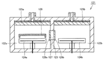
図34は、この場合のプラズマ処理装置の一部を示す概略断面図である。図34を参照して、プラズマ処理装置121は、図34中の左方側に位置する第一の処理空間122aと、右方側に位置する第二の処理空間122bとを備える。第一の処理空間122aと第二の処理空間122bとは、その間に位置する側壁123を共有するようにして設けられている。そして、各処理空間122a、122bにはそれぞれ、支持台124a、124b、プラズマ処理用ガス供給部および誘電体窓125a、125b等が設けられている。そして、各処理空間122a、122b内でそれぞれ、被処理基板Wに対するプラズマ処理が可能である。しかし、ヘッド部126を含むガス供給機構については、プラズマ処理装置において、1つのみ設けられている。
FIG. 34 is a schematic sectional view showing a part of the plasma processing apparatus in this case. Referring to FIG. 34,
ここで、第一の処理空間122aと第二の処理空間122bとの間に位置する側壁123の一部は、開口している。この開口部127を通じて、ヘッド部126は、第一の処理空間122aと第二の処理空間122bとの間を移動可能に構成されている。また、第一および第二の処理空間122a、122b側には、開口部127の開閉を可能とする第一のシャッター128a、および第二のシャッター128bが設けられている。具体的には、開口部127を通じて、ヘッド部126は、第一の処理空間122aと第二の処理空間122bとの間を行き来可能とされている。
Here, a part of the
このような構成によると、効率的な成膜工程を行なうことができる。すなわち、例えば、一方側である第二の処理空間122bで被処理基板Wのプラズマ処理を行っている間に、他方側である第一の処理空間122aにヘッド部126を移動させて、第一の処理空間122a内で、ヘッド部126により被処理基板Wに対するガス吸着工程を行う。このように構成することにより、効率的な成膜が可能となる。この場合、プラズマ発生器等についても、2つの処理空間における処理で、共用することができる。もちろん処理容器等を2つ以上設け、2つ以上の処理空間としてもよい。
According to such a configuration, an efficient film forming process can be performed. That is, for example, while the plasma processing of the substrate W to be processed is performed in the
なお、プラズマ処理装置は、支持台上への被処理基板の支持および支持台上に支持された被処理基板の取り外しのうちの少なくともいずれか一方が可能である被処理基板移動機構を備えるよう構成してもよい。図35は、この場合におけるプラズマ処理システムの構成を概略的に示す概略図である。図35を参照して、プラズマ処理システム161は、処理前の被処理基板Wの搬入口や処理後の被処理基板Wの搬出口となり、プラズマ処理システム161と外部との間において被処理基板Wの出し入れを行うための3つのロードポート162a、162b、162cと、大気圧雰囲気下において被処理基板Wの搬送を行う空間を有するロードモジュール163と、ロードモジュール163とトランスファモジュール165との間において圧力調整等を行う2つのロードロックモジュール164a、164bと、真空雰囲気下において被処理基板Wの搬送を行う空間を有するトランスファモジュール165と、被処理基板Wのプラズマ処理を行う2つのプラズマ処理装置181a、181bと、トランスファモジュール165の内部に備えられ、図示しないアームを用いて、プラズマ処理装置181a、181bとの間において被処理基板Wの出し入れ等の搬送を行う被処理基板搬送機構(図示せず)とを備える。
The plasma processing apparatus is configured to include a target substrate moving mechanism capable of at least one of supporting the target substrate on the support base and removing the target substrate supported on the support base. May be. FIG. 35 is a schematic diagram schematically showing the configuration of the plasma processing system in this case. Referring to FIG. 35, the
各プラズマ処理装置181a、181bに備えられるそれぞれの支持台167a、167bは、それぞれ4枚の被処理基板Wを載置するようにして支持することができる。支持台167aにおける4枚の被処理基板Wの支持領域を、図35等における一点鎖線で示す領域168a、168b、168c、168dで示している。また、支持台167bにおける4枚の被処理基板Wの支持領域を、図35等における一点鎖線で示す領域168e、168f、168g、168hで示している。なお、ここでは支持台167a、167bは、4枚の被処理基板Wを載置できることとしたが、これに囚われず、例えば、2枚以上の被処理基板Wを載置できるようにしてもよい。
Each of the
図36は、支持台167a付近を概略的に示す概略斜視図である。図36を参照して、被処理基板Wの支持台167a上への支持および被処理基板Wの支持台167aからの取り外しについては、3つのピン(図示せず)が用いられる。ピンによる被処理基板Wの支持および取り外しについては、後述する。なお、図36においては、支持台167aの領域168aにおける3つのピンの設置領域となる3つのピン孔172a、172b、172cを示している。他の領域168b〜168dにおけるピン孔の図示は省略する。3つのピン孔172a〜172cは、それぞれを仮想線で結んだ場合に、ほぼ正三角形を形成する位置に設けられている。すなわち、3つのピン孔172a〜172cは、仮想の正三角形の角に位置する部分に設けられている。
FIG. 36 is a schematic perspective view schematically showing the vicinity of the
支持台167aを備える一方のプラズマ処理装置181aには、上述したヘッド部169が設けられている。ヘッド部169は、支持部170に取り付けられている。ヘッド部169は、支持部170の外方側端部となる根元部171を回転中心として、図36中の矢印J1で示す方向に360度回転可能である。こうすることにより、4つの領域168a〜168dにそれぞれ支持された被処理基板Wにおいて、成膜等の処理を効率的に行うことができる。また、支持台167aは、根元部171の中心を回転中心として、図36中の矢印J2で示す方向に360度回転可能である。
One plasma processing apparatus 181a including the
こうすることにより、処理を行う被処理基板Wの搬入、すなわち、支持台167a上への支持や、処理が終了した被処理基板Wの搬出、すなわち、支持台167a上からの取り外しを効率的に行うことができる。ここで、上記した回転する支持台167aおよびピンは、支持台上への被処理基板の支持および支持台上に支持された被処理基板の取り外しのうちの少なくともいずれか一方が可能である被処理基板移動機構として作動する。すなわち、プラズマ処理装置は、支持台上への被処理基板の支持および支持台上に支持された被処理基板の取り外しのうちの少なくともいずれか一方が可能である被処理基板移動機構としての支持台およびピンを含む。
By doing so, it is possible to efficiently carry in the substrate W to be processed, that is, support on the
また、図37を参照して、支持台167bを備える他方のプラズマ処理装置181bについても、上述したヘッド部173、支持部174a、および根元部175が設けられている。そして、根元部175を中心としてヘッド部173と180度対向する位置に、被処理基板Wをその上に載置することができる載置部176が設けられている。載置部176は、支持部174bによって支持されている。ヘッド部173を支持する支持部174aと載置部176を支持する支持部174bとは、根元部175を間に挟んで、ほぼ一直線に連なるように設けられている。
Referring to FIG. 37, the above-described
載置部176は、断面L字状であって、回転中心軸方向から見た場合に、略半円状である。載置部176は、断面L字状の上面において、被処理基板Wを載置することができる。根元部175の回転により、ヘッド部173および載置部176は、根元部175の中心を回転中心として360度回転することができる。すなわち、所定の箇所を根元部175として、所定の箇所を基準として載置部176は、相対的に回転可能である。そして、所定の箇所を基準とした載置部176の相対的な回転運動により、支持台167b上への被処理基板Wの支持および支持台167b上に支持された被処理基板Wの取り外しを行う。こうすることにより、支持台167bが固定されており、支持台167bが回転できない構成であったとしても、4つの支持領域168e〜168hに支持された被処理基板Wの搬入および搬出を行うことができる。なお、図37においては、支持台167bの領域168eにおける3つのピンの設置領域となる3つのピン孔177a、177b、177cを示している。他の領域168f〜168hにおけるピン孔およびピンの図示については、省略する。なお、所定の箇所を基準とした載置部176の相対的な回転運動により、支持台167b上への被処理基板Wの支持および支持台167b上に支持された被処理基板Wの取り外しのうちの少なくともいずれか一方を行う構成としてもよい。
The mounting
ここで、ピンによる被処理基板Wの支持および取り外しについて説明すると、以下の通りである。図38、図39、図40、および図41は、ピンによる被処理基板Wの支持および取り外しを行う際の支持台167bの一部を示す概略断面図である。まず、図38を参照して、支持台167bの上の領域168eに被処理基板Wが支持されている。被処理基板Wが支持された領域168eには、ピン178a、178bおよびピン孔177a、177bが設けられている。ピン178a、178bはそれぞれ、ピン孔177a、177b内に設けられている。なお、図38〜図41においては、理解の容易の観点から、ピン孔177cおよびピン孔177c内に設けられているピンの図示については、省略する。ピン178a、178bは、図38における紙面上下方向に移動可能である。
Here, the support and removal of the substrate W to be processed by the pins will be described as follows. 38, 39, 40, and 41 are schematic cross-sectional views showing a part of the
次に、図39を参照して、ピン孔177a、177b内に配置されたピン178a、178bがそれぞれ紙面上方向に移動する。そうすると、被処理基板Wの下面179をピン178a、178bの上側端部で押し、被処理基板Wが上方向に移動する。この場合、被処理基板Wは、ピン178a、178bの上側端部に載るような状態となるが、ピンは合計3つあるので、いわゆる三点支持の形となり、比較的安定して被処理基板Wを載せることができる。
Next, referring to FIG. 39, the
次に、図40を参照して、載置部176が支持領域168eの位置まで回転して移動する。そうすると、被処理基板Wの下面179が載置部176における断面L字状の上面180に対向する位置にくる。なお、図40においては、載置部176のうち、外方側に位置する部分が回転により早く到達するため、外方側に位置する部分を実線で示し、内方側に位置する部分を点線で示している。
Next, with reference to FIG. 40, the mounting
次に、図41に示す状態で、ピン178a、178bを下方向に移動する。そうすると、載置部176の上面180上に被処理基板Wの下面179が載置される。そして、載置部176の回転により、支持領域168e外に被処理基板Wが移動させられる。
Next, in the state shown in FIG. 41, the
なお、被処理基板Wの支持台167bへの支持については、上記したように載置部176により所定の位置、例えば、被処理基板Wが領域168fに移動させられた後、ピンが上昇し、被処理基板Wを持ち上げた状態で、載置部176を回転させて領域168f外に移動し、その後、ピンを下降させることにより、領域168fに支持させることができる。
For supporting the substrate W to be processed on the
こうすることにより、支持台167bが回転せず、固定されている状態によっても、被処理基板Wの支持台167b上への支持および支持台167bからの取り外しを効率的に行うことができる。
By doing so, even if the
ここで、上記した載置部およびピンは、支持台上への被処理基板の支持および支持台上に支持された被処理基板の取り外しのうちの少なくともいずれか一方が可能である被処理基板移動機構として作動する。すなわち、プラズマ処理装置は、支持台上への被処理基板の支持および支持台上に支持された被処理基板の取り外しのうちの少なくともいずれか一方が可能である被処理基板移動機構としての載置部およびピンを含む。 Here, the mounting portion and the pins described above can move the substrate to be processed so that at least one of the support of the substrate to be processed on the support base and the removal of the substrate to be processed supported on the support base is possible. Acts as a mechanism. In other words, the plasma processing apparatus is placed as a target substrate moving mechanism capable of at least one of supporting the target substrate on the support base and removing the target substrate supported on the support base. Includes parts and pins.
なお、上記の実施の形態においては、各領域において、3つのピンおよびピン孔を設ける構成としたが、これに限らず、4つ以上のピン等を設ける構成にしてもよい。さらには、安定した状態でピンの上側端部に載せることができればよく、3つのピンを正三角形の位置に必ずしも設けなくともよい。また、例えば、ピンの先端が平板状でもよく、この場合、ピンの数は、1つまたは2つであっても安定した状態で被処理基板Wを一時的に載せることができる。 In the above embodiment, each region has three pins and pin holes. However, the present invention is not limited to this, and four or more pins may be provided. Furthermore, it is only necessary that the pin can be placed on the upper end of the pin in a stable state, and the three pins are not necessarily provided at the position of the equilateral triangle. Further, for example, the tip of the pin may be flat, and in this case, the substrate W to be processed can be temporarily placed in a stable state even if the number of pins is one or two.
なお、上記の実施の形態において、支持台を上下方向および左右方向の少なくともいずれか一方側に移動可能なように構成することにしてもよい。こうすることにより、より適切に、プラズマ処理やガス吸着を行うことができる。具体的には、例えば、ヘッド部を第一の位置に配置させる際に、ヘッド部の移動に連動させて、支持台をヘッド部に近づけるように移動させるようにする。 In the above embodiment, the support base may be configured to be movable in at least one of the vertical direction and the horizontal direction. By carrying out like this, plasma processing and gas adsorption can be performed more appropriately. Specifically, for example, when the head unit is arranged at the first position, the support base is moved closer to the head unit in conjunction with the movement of the head unit.
また、上記したプラズマ処理装置において、ガスの置換性を改善させるため、ヘッド部から供給する成膜ガスおよびパージガスのうち、同一のガスであるアルゴンガスを継続して供給するようにしたが、これについて説明すると以下の通りである。上記の実施の形態においては、ヘッド部から供給されるガスのうち、成膜ガスは、希釈用のアルゴンガスとプリカーサガスとの混合ガスであり、パージガスは、アルゴンガスである。つまり、アルゴンガスを、継続して供給するようにしてもよい。さらに、ヘッド部が退避する際も、継続してパージガスを供給している。これによると、成膜ガスおよびパージガスが供給されていない間に、プラズマがガス供給孔68やガス供給路69内に侵入するおそれがない。なお、上記の実施の形態においては、プラズマ処理用のガスは、アルゴンガスと酸素(O2)ガスとの混合ガスであるため、例え、ヘッド部からアルゴンガスを継続して供給していても、プラズマ処理に影響を与えない。つまり、プラズマ処理用のガス、成膜ガス、パージガスのそれぞれ少なくとも一つのガスは、同一のガスであることが好ましい。
Further, in the plasma processing apparatus described above, in order to improve the gas substituting property, argon gas, which is the same gas among the film forming gas and purge gas supplied from the head portion, is continuously supplied. Is described as follows. In the above embodiment, among the gases supplied from the head unit, the film forming gas is a mixed gas of dilution argon gas and precursor gas, and the purge gas is argon gas. That is, you may make it supply argon gas continuously. Further, the purge gas is continuously supplied even when the head portion is retracted. According to this, there is no possibility that plasma enters the
なお、上記の実施の形態においては、ヘッド部から供給する成膜ガスおよびパージガスのうち、同一のガスを継続して供給するようにしたが、これに限らず、適宜タイミングを合わせてガスを供給するようにしてもよい。また、ヘッド部が退避している際にパージガスを供給しなくてもよい。 In the above embodiment, the same gas is continuously supplied among the film forming gas and the purge gas supplied from the head unit. However, the present invention is not limited to this, and the gas is supplied at an appropriate timing. You may make it do. Further, it is not necessary to supply the purge gas when the head portion is retracted.
なお、上記の実施の形態においては、シリコン原子を酸化する場合について説明したが、これに限らず、シリコン原子を窒化する場合についても適用される。すなわち、上記したガス吸着工程の後に、窒化物を含むガス、例えば、N2ガスやNH3ガスを処理容器内に供給してプラズマ処理を行い、シリコン窒化膜を形成する。このような場合についても適用される。 In the above-described embodiment, the case where silicon atoms are oxidized has been described. However, the present invention is not limited to this, and the present invention is also applicable to the case where silicon atoms are nitrided. That is, after the gas adsorption step described above, a nitride-containing gas, for example, N 2 gas or NH 3 gas is supplied into the processing vessel and plasma treatment is performed to form a silicon nitride film. This also applies to such a case.
また、上記の実施の形態においては、ガス吸着用のプリカーサガスとしてBTBASを含むガスを用いることとしたが、アミノシラン系のガス、ジクロロシラン(DCS(Dichlorosilane):SiH2CL2)、ヘキサクロロジシラン(HCD(Hexachlorodisilane):Si2Cl6)などのハロゲンを含むガス、金属元素を含むALD用ガスを用いても構わない。また、プラズマ処理においても、一酸化炭素等の酸素原子を含むガス以外のガスを用いることも可能である。 In the above embodiment, a gas containing BTBAS is used as a precursor gas for gas adsorption. However, an aminosilane-based gas, dichlorosilane (DCS (Dichlorosilane): SiH 2 CL 2 ), hexachlorodisilane ( A gas containing halogen, such as HCD (Hexachlorodisilene): Si 2 Cl 6 ), or an ALD gas containing a metal element may be used. In the plasma treatment, a gas other than a gas containing oxygen atoms such as carbon monoxide can be used.
なお、上記の実施形態において、ヘッド部の移動に関わらず、プラズマを常に生成した状態として説明したが、スループットを勘案し、プラズマの連続した生成を中断することもできる。この場合であっても、成膜ガスがヘッド部内の小容積領域Sから処理容器内へ過剰に供給されることを抑制することができる。 In the above embodiment, the plasma is always generated regardless of the movement of the head portion. However, the continuous generation of plasma can be interrupted in consideration of the throughput. Even in this case, it is possible to suppress an excessive supply of the film forming gas from the small volume region S in the head portion into the processing container.
なお、上記の実施の形態においては、素子分離領域においてトレンチを形成し、穴埋め絶縁膜によりトレンチを埋める前にトレンチの表面に形成されるライナー膜を形成する場合について説明したが、これに限らず、例えば、MOSトランジスタにおけるゲート酸化膜や他の絶縁層、例えば、層間絶縁膜やゲート側壁部の形成に適用してもよい。さらに、CCDやLSI等においても、もちろん有効に適用される。すなわち、成膜ガスを供給して吸着層を形成するガス吸着工程とプラズマ処理工程を組み合わせて行う全ての成膜プロセスに適用される。 In the above-described embodiment, the case where the trench is formed in the element isolation region and the liner film formed on the surface of the trench is formed before the trench is filled with the hole-filling insulating film has been described. For example, the present invention may be applied to formation of a gate oxide film or other insulating layer in a MOS transistor, for example, an interlayer insulating film or a gate sidewall. Of course, the present invention is also effectively applied to CCDs and LSIs. In other words, the present invention is applied to all film forming processes in which a gas adsorption process for supplying a film forming gas to form an adsorption layer and a plasma treatment process are combined.
具体的な膜としては以下のものが挙げられる。すなわち、ゲート絶縁膜として、SiO2、Al2O3、HfO2、ZrO2、Ta2O5、La2O3、DRAM(Dynamic Random Access Memory)のトレンチキャパシターとして、SiO2、HfO2、Al2O3、Ta2O5、FinFET(Field Effect Transistor)等の3Dデバイスのゲート酸化膜として、SiO2、Al2O3、HfO2、ZrO2、Ta2O5、La2O3、MEMS(Micro Electro Mechanical Systems)ナノラミネートとして、HfO2、Ta2O5、TiO2、Ta2O5、Al2O3、UVブロックレイヤーとしてZnO、TiO2、有機EL(Electro Luminescence)素子としてアルミナ絶縁膜であるAl2O3、オプティカルデバイスや太陽電池等として、AlTiO、SnO2、ZnO、圧電素子としてZnO等が挙げられる。
Specific examples of the film include the following. That is, as a gate insulating film, SiO 2 , H 2 O 3 , HfO 2 , ZrO 2 , Ta 2 O 5 , La 2 O 3 , DRAM (Dynamic Random Access Memory) as a trench capacitor, SiO 2 , HfO 2 , Al As gate oxide films for 3D devices such as 2 O 3 , Ta 2 O 5 , FinFET (Field Effect Transistor), etc., SiO 2 , Al 2 O 3 , HfO 2 , ZrO 2 , Ta 2 O 5 , La 2 O 3 , MEMS as (Micro Electro Mechanical Systems) nanolaminate, HfO 2, Ta 2 O 5 ,
なお、上記の実施の形態において、ガス吸着工程とプラズマ処理工程との間に、処理容器内を排気する排気工程を行ってもよい。さらに、プラズマ処理工程の後に、排気工程を行ってもよい。 In the above embodiment, an exhaust process for exhausting the inside of the processing container may be performed between the gas adsorption process and the plasma processing process. Further, an exhaust process may be performed after the plasma treatment process.
また、上記の実施の形態においては、プラズマ処理用のガスは、側壁に設けられたガス供給孔から供給することにしたが、これに限らず、被処理基板の中央に向かって噴出するガス供給孔を、例えば、誘電体窓の中央領域に設け、このガス供給孔から供給することにしてもよい。 In the above embodiment, the plasma processing gas is supplied from the gas supply hole provided in the side wall. However, the present invention is not limited thereto, and the gas supply is jetted toward the center of the substrate to be processed. For example, the hole may be provided in the central region of the dielectric window and supplied from the gas supply hole.
また、上記の実施の形態においては、スロットアンテナ板を用いたRLSAによるマイクロ波によりプラズマ処理を行うこととしたが、これに限らず、くし型のアンテナ部を有するマイクロ波プラズマ処理装置を用いてもよい。 Further, in the above embodiment, the plasma processing is performed by the microwave by RLSA using the slot antenna plate. However, the present invention is not limited to this, and the microwave plasma processing apparatus having a comb-shaped antenna unit is used. Also good.
なお、上記の実施の形態においては、マイクロ波をプラズマ源とするプラズマ処理装置であったが、これに限らず、ICP(Inductively−coupled Plasma)やECR(Electron Cyclotron Resoannce)プラズマ、平行平板型プラズマ等をプラズマ源とするプラズマ処理装置等についても適用され、プラズマ生成手段に限定されない。 In the above-described embodiment, the plasma processing apparatus uses a microwave as a plasma source. However, the present invention is not limited thereto, and is not limited to ICP (Inductively-coupled Plasma), ECR (Electron Cyclotron Resonance) plasma, or parallel plate plasma. The present invention is also applicable to a plasma processing apparatus using a plasma source as a plasma source, and is not limited to plasma generation means.
また、上記の実施の形態においては、シリコン酸化膜等の絶縁膜を成膜する場合について説明したが、これに限らず、導電膜を成膜する場合についても適用される。 In the above embodiment, the case where an insulating film such as a silicon oxide film is formed has been described. However, the present invention is not limited to this, and the present invention is also applicable to the case where a conductive film is formed.
以上、図面を参照してこの発明の実施形態を説明したが、この発明は、図示した実施形態のものに限定されない。図示した実施形態に対して、この発明と同一の範囲内において、あるいは均等の範囲内において、種々の修正や変形を加えることが可能である。 As mentioned above, although embodiment of this invention was described with reference to drawings, this invention is not limited to the thing of embodiment shown in figure. Various modifications and variations can be made to the illustrated embodiment within the same range or equivalent range as the present invention.
11 MOS型半導体素子、12 シリコン基板、13 素子分離領域、14a p型ウェル、14b n型ウェル、15a 高濃度n型不純物拡散領域、15b 高濃度p型不純物拡散領域、16a n型不純物拡散領域、16b p型不純物拡散領域、17 ゲート酸化膜、18 ゲート電極、19 ゲート側壁部、21 絶縁膜、22 コンタクトホール、23 穴埋め電極、24 メタル配線層、26,27,168a,168b,168c,168d,168e,168f,168g,168h 領域、31,81a,81b,81c,81d,81e,81f,81g,81h,81j,91,111,116,121,181a,181b プラズマ処理装置、32,92,115,119 処理容器、33 ガス供給部、34,83a,83b,83c,83d,83e,83f,83g,83h,97,124a,124b,167a,167b 支持台、35 マイクロ波発生器、36,125a,125b 誘電体窓、37 スロットアンテナ板、38 誘電体部材、39 プラズマ発生機構、40 スロット孔、41 底部、42,123 側壁、43 排気孔、44 蓋部、45 Oリング、46,68,79,80,86c,86d,86e,86f,86g,86h ガス供給孔、47,180 上面、48,63,74,179 下面、49 筒状支持部、51 マッチング機構、52 モード変換器、53 導波管、54 同軸導波管、55a,55b 供給系統、56a,56b MFC、57a,57b,57c,57d,57e バルブ、58a,58b パイプ、61 ガス供給機構、62,82a,82b,82c,82d,82e,82f,82g,82h,93,112,117,169,173 ヘッド部、64 遮断機構、65,95 端部、66,94,113,118,126,170,174a,174b 支持部、67,73 延出部、69,87c,87d,87e,87f,87h,155 ガス供給路、70,84a,84b,84c,84d,84e,84f,84g,84h,86b ガス排気孔、71,85a,85b,85c,85d,85e,85f,85h,87b,156 ガス排気路、72 ガス排気機構、75 パージガス供給機構、 76 収容部、77 遮蔽板、78,96 内壁面、82j,83j 排気系統、84j,86j ドライポンプ、85j,87j 配管、88a フォーカスリング、88g,89g 壁面、88h 支持台外方部材、88j 除害装置、89h 外周面、90h 内周面、151 可動部、152 固定部、153 ベース、154 回転中心軸、122a,122b 処理空間、127 開口部、128a,128b シャッター、161 プラズマ処理システム、162a,162b,162c ロードポート、163 ロードモジュール、164a,164b ロードロックモジュール、165 トランスファモジュール、171,175 根元部、172a,172b,172c,177a,177b,177c ピン孔、176 載置部、178a,178b ピン。 11 MOS type semiconductor element, 12 silicon substrate, 13 element isolation region, 14a p type well, 14b n type well, 15a high concentration n type impurity diffusion region, 15b high concentration p type impurity diffusion region, 16a n type impurity diffusion region, 16b p-type impurity diffusion region, 17 gate oxide film, 18 gate electrode, 19 gate side wall, 21 insulating film, 22 contact hole, 23 buried electrode, 24 metal wiring layer, 26, 27, 168a, 168b, 168c, 168d, 168e, 168f, 168g, 168h region, 31, 81a, 81b, 81c, 81d, 81e, 81f, 81g, 81h, 81j, 91, 111, 116, 121, 181a, 181b plasma processing apparatus, 32, 92, 115, 119 processing vessel, 33 gas supply unit, 34, 83a, 8 3b, 83c, 83d, 83e, 83f, 83g, 83h, 97, 124a, 124b, 167a, 167b Support base, 35 microwave generator, 36, 125a, 125b Dielectric window, 37 slot antenna plate, 38 Dielectric member , 39 Plasma generating mechanism, 40 slot hole, 41 bottom, 42, 123 side wall, 43 exhaust hole, 44 lid, 45 O-ring, 46, 68, 79, 80, 86c, 86d, 86e, 86f, 86g, 86h gas Supply hole, 47, 180 upper surface, 48, 63, 74, 179 lower surface, 49 cylindrical support, 51 matching mechanism, 52 mode converter, 53 waveguide, 54 coaxial waveguide, 55a, 55b supply system, 56a , 56b MFC, 57a, 57b, 57c, 57d, 57e Valve, 58a, 58b Pipe, 61 Gas supply mechanism 62, 82a, 82b, 82c, 82d, 82e, 82f, 82g, 82h, 93, 112, 117, 169, 173 Head part, 64 shut off mechanism, 65, 95 end part, 66, 94, 113, 118, 126, 170, 174a, 174b Support part, 67, 73 Extension part, 69, 87c, 87d, 87e, 87f, 87h, 155 Gas supply path, 70, 84a, 84b, 84c, 84d, 84e, 84f, 84g, 84h, 86b gas exhaust holes, 71, 85a, 85b, 85c, 85d, 85e, 85f, 85h, 87b, 156 gas exhaust passages, 72 gas exhaust mechanisms, 75 purge gas supply mechanisms, 76 housing parts, 77 shielding plates, 78, 96 Inner wall surface, 82j, 83j Exhaust system, 84j, 86j Dry pump, 85j, 87j Piping 88a Focus ring, 88g, 89g wall surface, 88h support base outer member, 88j abatement device, 89h outer peripheral surface, 90h inner peripheral surface, 151 movable part, 152 fixed part, 153 base, 154 rotation center axis, 122a, 122b Space, 127 opening, 128a, 128b shutter, 161 plasma processing system, 162a, 162b, 162c load port, 163 load module, 164a, 164b load lock module, 165 transfer module, 171, 175 root, 172a, 172b, 172c , 177a, 177b, 177c pin hole, 176 mounting portion, 178a, 178b pin.
Claims (17)
前記処理容器内に配置され、その上に前記被処理基板を支持する支持台と、
前記処理容器内にプラズマを発生させるプラズマ発生手段と、
前記支持台の上方側を覆って前記支持台との間に小容積領域を形成可能な第一の位置および前記第一の位置と異なる第二の位置に移動可能であって、成膜ガスを供給する第一のガス供給孔が一方面側に開口するように設けられている板状のヘッド部を有し、成膜ガスの供給を行う成膜ガス供給機構と、
前記ヘッド部が前記第一の位置にあるときに前記処理容器内の空間から前記小容積領域を遮断する遮断機構とを備える、プラズマ処理装置。 Including a bottom portion located on the lower side and a side wall extending upward from the outer peripheral side of the bottom portion, and a processing container capable of being sealed and performing plasma processing on the substrate to be processed therein,
A support base disposed in the processing container and supporting the substrate to be processed thereon;
Plasma generating means for generating plasma in the processing vessel;
A first position that covers the upper side of the support base and can form a small volume region between the support base and a second position different from the first position, the film formation gas being A film-forming gas supply mechanism for supplying a film-forming gas, having a plate-like head portion provided so that the first gas supply hole to be supplied opens on one surface side;
A plasma processing apparatus, comprising: a blocking mechanism that blocks the small volume region from a space in the processing container when the head portion is at the first position.
前記パージガス供給機構は、前記支持台の外方側に設けられ、前記第二のガス供給孔が設けられたパージガス供給部材を含む、請求項3〜6のいずれかに記載のプラズマ処理装置。 The gas exhaust hole is provided in the head portion,
The plasma processing apparatus according to claim 3, wherein the purge gas supply mechanism includes a purge gas supply member provided on an outer side of the support base and provided with the second gas supply hole.
前記成膜ガス供給機構は、前記支持台上に支持された被処理基板の外方側で前記ガス排気孔に対向する位置であって、前記支持台の上に着脱可能なフォーカスリングを含む、請求項2〜8のいずれかに記載のプラズマ処理装置。 The gas exhaust hole is provided in the head portion,
The film forming gas supply mechanism includes a focus ring that is detachable on the support base at a position facing the gas exhaust hole on the outer side of the substrate to be processed supported on the support base. The plasma processing apparatus in any one of Claims 2-8.
前記ガス排気機構は、前記支持部の内部に設けられ、前記ガス排気孔に通じ、排気されたガスの通路となるガス排気路を含み、
前記成膜ガス供給機構は、前記支持部の内部に設けられ、前記第一のガス供給孔に通じ、供給する成膜ガスの通路となる第一のガス供給路を含み、
前記第一のガス供給路は、前記ガス排気路の内側となるように多重に設けられている、請求項2〜9のいずれかに記載のプラズマ処理装置。 The film forming gas supply mechanism includes a support portion that extends from the side wall and is connected to the head portion and supports the head portion,
The gas exhaust mechanism includes a gas exhaust path that is provided inside the support portion, communicates with the gas exhaust hole, and serves as a path for exhausted gas,
The film forming gas supply mechanism includes a first gas supply path that is provided inside the support portion, communicates with the first gas supply hole, and serves as a passage for a film forming gas to be supplied.
The plasma processing apparatus according to claim 2, wherein the first gas supply path is provided in multiple so as to be inside the gas exhaust path.
前記第二のガス供給孔は、前記ヘッド部に設けられており、
前記ガス排気機構は、前記ヘッド部が前記処理容器内に位置するときにガスを排気し、
前記パージガス供給機構は、前記ヘッド部が前記収容部に位置するときに前記パージガスを供給する、請求項2〜10のいずれかに記載のプラズマ処理装置。 The processing container is formed such that a part of the side wall extends outward, and is provided with an accommodating portion capable of accommodating the head portion,
The second gas supply hole is provided in the head portion,
The gas exhaust mechanism exhausts gas when the head portion is located in the processing container,
The plasma processing apparatus according to claim 2, wherein the purge gas supply mechanism supplies the purge gas when the head unit is located in the housing unit.
前記所定の箇所を基準とした前記載置部の相対的な回転運動により、前記支持台上への前記被処理基板の支持および前記支持台上に支持された前記被処理基板の取り外しのうちの少なくともいずれか一方を行う、請求項13に記載のプラズマ処理装置。 The processing substrate moving mechanism includes a mounting portion on which a processing substrate can be mounted and is relatively rotatable with reference to a predetermined location.
Of the support of the substrate to be processed on the support base and the removal of the substrate to be processed supported on the support base by the relative rotational movement of the mounting portion with respect to the predetermined location The plasma processing apparatus according to claim 13, wherein at least one of them is performed.
前記第一の排気系統と前記第二の排気系統とは、それぞれ別個に設けられている、請求項1〜14のいずれかに記載のプラズマ処理装置。 A first exhaust system for exhausting the processing container, and a second exhaust system for exhausting the small volume region,
The plasma processing apparatus according to claim 1, wherein the first exhaust system and the second exhaust system are provided separately.
17. The plasma according to claim 16, wherein the plasma generating means includes a slot antenna plate that is provided with a plurality of slot holes, is disposed above the dielectric window, and radiates microwaves to the dielectric window. Processing equipment.
Priority Applications (1)
| Application Number | Priority Date | Filing Date | Title |
|---|---|---|---|
| JP2011059763A JP2012195513A (en) | 2011-03-17 | 2011-03-17 | Plasma processing apparatus |
Applications Claiming Priority (1)
| Application Number | Priority Date | Filing Date | Title |
|---|---|---|---|
| JP2011059763A JP2012195513A (en) | 2011-03-17 | 2011-03-17 | Plasma processing apparatus |
Publications (1)
| Publication Number | Publication Date |
|---|---|
| JP2012195513A true JP2012195513A (en) | 2012-10-11 |
Family
ID=47087109
Family Applications (1)
| Application Number | Title | Priority Date | Filing Date |
|---|---|---|---|
| JP2011059763A Withdrawn JP2012195513A (en) | 2011-03-17 | 2011-03-17 | Plasma processing apparatus |
Country Status (1)
| Country | Link |
|---|---|
| JP (1) | JP2012195513A (en) |
Cited By (251)
| Publication number | Priority date | Publication date | Assignee | Title |
|---|---|---|---|---|
| JP2015078418A (en) * | 2013-10-18 | 2015-04-23 | 東京エレクトロン株式会社 | Film deposition method, and film deposition apparatus |
| JP2016076620A (en) * | 2014-10-07 | 2016-05-12 | 東京エレクトロン株式会社 | Method of processing workpiece |
| JP2016134623A (en) * | 2015-01-16 | 2016-07-25 | エーエスエム アイピー ホールディング ビー.ブイ. | Plasma-enhanced atomic layer etching method |
| CN110468389A (en) * | 2018-05-10 | 2019-11-19 | 三星电子株式会社 | Depositing device |
| US10590535B2 (en) | 2017-07-26 | 2020-03-17 | Asm Ip Holdings B.V. | Chemical treatment, deposition and/or infiltration apparatus and method for using the same |
| US10600673B2 (en) | 2015-07-07 | 2020-03-24 | Asm Ip Holding B.V. | Magnetic susceptor to baseplate seal |
| US10604847B2 (en) | 2014-03-18 | 2020-03-31 | Asm Ip Holding B.V. | Gas distribution system, reactor including the system, and methods of using the same |
| US10612136B2 (en) | 2018-06-29 | 2020-04-07 | ASM IP Holding, B.V. | Temperature-controlled flange and reactor system including same |
| US10643826B2 (en) | 2016-10-26 | 2020-05-05 | Asm Ip Holdings B.V. | Methods for thermally calibrating reaction chambers |
| US10643904B2 (en) | 2016-11-01 | 2020-05-05 | Asm Ip Holdings B.V. | Methods for forming a semiconductor device and related semiconductor device structures |
| US10658205B2 (en) | 2017-09-28 | 2020-05-19 | Asm Ip Holdings B.V. | Chemical dispensing apparatus and methods for dispensing a chemical to a reaction chamber |
| US10655221B2 (en) | 2017-02-09 | 2020-05-19 | Asm Ip Holding B.V. | Method for depositing oxide film by thermal ALD and PEALD |
| US10658181B2 (en) | 2018-02-20 | 2020-05-19 | Asm Ip Holding B.V. | Method of spacer-defined direct patterning in semiconductor fabrication |
| US10665452B2 (en) | 2016-05-02 | 2020-05-26 | Asm Ip Holdings B.V. | Source/drain performance through conformal solid state doping |
| US10672636B2 (en) | 2017-08-09 | 2020-06-02 | Asm Ip Holding B.V. | Cassette holder assembly for a substrate cassette and holding member for use in such assembly |
| US10685834B2 (en) | 2017-07-05 | 2020-06-16 | Asm Ip Holdings B.V. | Methods for forming a silicon germanium tin layer and related semiconductor device structures |
| US10683571B2 (en) | 2014-02-25 | 2020-06-16 | Asm Ip Holding B.V. | Gas supply manifold and method of supplying gases to chamber using same |
| US10692741B2 (en) | 2017-08-08 | 2020-06-23 | Asm Ip Holdings B.V. | Radiation shield |
| US10707106B2 (en) | 2011-06-06 | 2020-07-07 | Asm Ip Holding B.V. | High-throughput semiconductor-processing apparatus equipped with multiple dual-chamber modules |
| US10714315B2 (en) | 2012-10-12 | 2020-07-14 | Asm Ip Holdings B.V. | Semiconductor reaction chamber showerhead |
| US10714350B2 (en) | 2016-11-01 | 2020-07-14 | ASM IP Holdings, B.V. | Methods for forming a transition metal niobium nitride film on a substrate by atomic layer deposition and related semiconductor device structures |
| US10714335B2 (en) | 2017-04-25 | 2020-07-14 | Asm Ip Holding B.V. | Method of depositing thin film and method of manufacturing semiconductor device |
| US10714385B2 (en) | 2016-07-19 | 2020-07-14 | Asm Ip Holding B.V. | Selective deposition of tungsten |
| US10720322B2 (en) | 2016-02-19 | 2020-07-21 | Asm Ip Holding B.V. | Method for forming silicon nitride film selectively on top surface |
| US10720331B2 (en) | 2016-11-01 | 2020-07-21 | ASM IP Holdings, B.V. | Methods for forming a transition metal nitride film on a substrate by atomic layer deposition and related semiconductor device structures |
| US10734244B2 (en) | 2017-11-16 | 2020-08-04 | Asm Ip Holding B.V. | Method of processing a substrate and a device manufactured by the same |
| US10734223B2 (en) | 2017-10-10 | 2020-08-04 | Asm Ip Holding B.V. | Method for depositing a metal chalcogenide on a substrate by cyclical deposition |
| US10731249B2 (en) | 2018-02-15 | 2020-08-04 | Asm Ip Holding B.V. | Method of forming a transition metal containing film on a substrate by a cyclical deposition process, a method for supplying a transition metal halide compound to a reaction chamber, and related vapor deposition apparatus |
| US10734497B2 (en) | 2017-07-18 | 2020-08-04 | Asm Ip Holding B.V. | Methods for forming a semiconductor device structure and related semiconductor device structures |
| US10741385B2 (en) | 2016-07-28 | 2020-08-11 | Asm Ip Holding B.V. | Method and apparatus for filling a gap |
| US10755922B2 (en) | 2018-07-03 | 2020-08-25 | Asm Ip Holding B.V. | Method for depositing silicon-free carbon-containing film as gap-fill layer by pulse plasma-assisted deposition |
| US10755923B2 (en) | 2018-07-03 | 2020-08-25 | Asm Ip Holding B.V. | Method for depositing silicon-free carbon-containing film as gap-fill layer by pulse plasma-assisted deposition |
| US10770286B2 (en) | 2017-05-08 | 2020-09-08 | Asm Ip Holdings B.V. | Methods for selectively forming a silicon nitride film on a substrate and related semiconductor device structures |
| US10770336B2 (en) | 2017-08-08 | 2020-09-08 | Asm Ip Holding B.V. | Substrate lift mechanism and reactor including same |
| US10767789B2 (en) | 2018-07-16 | 2020-09-08 | Asm Ip Holding B.V. | Diaphragm valves, valve components, and methods for forming valve components |
| US10784102B2 (en) | 2016-12-22 | 2020-09-22 | Asm Ip Holding B.V. | Method of forming a structure on a substrate |
| US10787741B2 (en) | 2014-08-21 | 2020-09-29 | Asm Ip Holding B.V. | Method and system for in situ formation of gas-phase compounds |
| US10797133B2 (en) | 2018-06-21 | 2020-10-06 | Asm Ip Holding B.V. | Method for depositing a phosphorus doped silicon arsenide film and related semiconductor device structures |
| US10804098B2 (en) | 2009-08-14 | 2020-10-13 | Asm Ip Holding B.V. | Systems and methods for thin-film deposition of metal oxides using excited nitrogen-oxygen species |
| US10811256B2 (en) | 2018-10-16 | 2020-10-20 | Asm Ip Holding B.V. | Method for etching a carbon-containing feature |
| US10818758B2 (en) | 2018-11-16 | 2020-10-27 | Asm Ip Holding B.V. | Methods for forming a metal silicate film on a substrate in a reaction chamber and related semiconductor device structures |
| USD900036S1 (en) | 2017-08-24 | 2020-10-27 | Asm Ip Holding B.V. | Heater electrical connector and adapter |
| US10832903B2 (en) | 2011-10-28 | 2020-11-10 | Asm Ip Holding B.V. | Process feed management for semiconductor substrate processing |
| US10829852B2 (en) | 2018-08-16 | 2020-11-10 | Asm Ip Holding B.V. | Gas distribution device for a wafer processing apparatus |
| US10844486B2 (en) | 2009-04-06 | 2020-11-24 | Asm Ip Holding B.V. | Semiconductor processing reactor and components thereof |
| US10847366B2 (en) | 2018-11-16 | 2020-11-24 | Asm Ip Holding B.V. | Methods for depositing a transition metal chalcogenide film on a substrate by a cyclical deposition process |
| US10847365B2 (en) | 2018-10-11 | 2020-11-24 | Asm Ip Holding B.V. | Method of forming conformal silicon carbide film by cyclic CVD |
| US10844484B2 (en) | 2017-09-22 | 2020-11-24 | Asm Ip Holding B.V. | Apparatus for dispensing a vapor phase reactant to a reaction chamber and related methods |
| US10847371B2 (en) | 2018-03-27 | 2020-11-24 | Asm Ip Holding B.V. | Method of forming an electrode on a substrate and a semiconductor device structure including an electrode |
| US10854498B2 (en) | 2011-07-15 | 2020-12-01 | Asm Ip Holding B.V. | Wafer-supporting device and method for producing same |
| US10851456B2 (en) | 2016-04-21 | 2020-12-01 | Asm Ip Holding B.V. | Deposition of metal borides |
| USD903477S1 (en) | 2018-01-24 | 2020-12-01 | Asm Ip Holdings B.V. | Metal clamp |
| US10858737B2 (en) | 2014-07-28 | 2020-12-08 | Asm Ip Holding B.V. | Showerhead assembly and components thereof |
| US10867786B2 (en) | 2018-03-30 | 2020-12-15 | Asm Ip Holding B.V. | Substrate processing method |
| US10865475B2 (en) | 2016-04-21 | 2020-12-15 | Asm Ip Holding B.V. | Deposition of metal borides and silicides |
| US10867788B2 (en) | 2016-12-28 | 2020-12-15 | Asm Ip Holding B.V. | Method of forming a structure on a substrate |
| US10872771B2 (en) | 2018-01-16 | 2020-12-22 | Asm Ip Holding B. V. | Method for depositing a material film on a substrate within a reaction chamber by a cyclical deposition process and related device structures |
| US10883175B2 (en) | 2018-08-09 | 2021-01-05 | Asm Ip Holding B.V. | Vertical furnace for processing substrates and a liner for use therein |
| US10892156B2 (en) | 2017-05-08 | 2021-01-12 | Asm Ip Holding B.V. | Methods for forming a silicon nitride film on a substrate and related semiconductor device structures |
| US10896820B2 (en) | 2018-02-14 | 2021-01-19 | Asm Ip Holding B.V. | Method for depositing a ruthenium-containing film on a substrate by a cyclical deposition process |
| US10910262B2 (en) | 2017-11-16 | 2021-02-02 | Asm Ip Holding B.V. | Method of selectively depositing a capping layer structure on a semiconductor device structure |
| US10914004B2 (en) | 2018-06-29 | 2021-02-09 | Asm Ip Holding B.V. | Thin-film deposition method and manufacturing method of semiconductor device |
| US10923344B2 (en) | 2017-10-30 | 2021-02-16 | Asm Ip Holding B.V. | Methods for forming a semiconductor structure and related semiconductor structures |
| US10928731B2 (en) | 2017-09-21 | 2021-02-23 | Asm Ip Holding B.V. | Method of sequential infiltration synthesis treatment of infiltrateable material and structures and devices formed using same |
| US10934619B2 (en) | 2016-11-15 | 2021-03-02 | Asm Ip Holding B.V. | Gas supply unit and substrate processing apparatus including the gas supply unit |
| US10941490B2 (en) | 2014-10-07 | 2021-03-09 | Asm Ip Holding B.V. | Multiple temperature range susceptor, assembly, reactor and system including the susceptor, and methods of using the same |
| USD913980S1 (en) | 2018-02-01 | 2021-03-23 | Asm Ip Holding B.V. | Gas supply plate for semiconductor manufacturing apparatus |
| US10975470B2 (en) | 2018-02-23 | 2021-04-13 | Asm Ip Holding B.V. | Apparatus for detecting or monitoring for a chemical precursor in a high temperature environment |
| CN112680710A (en) * | 2019-10-18 | 2021-04-20 | 台湾积体电路制造股份有限公司 | Film deposition chamber, multifunctional shielding disc and using method of multifunctional shielding disc |
| US11004977B2 (en) | 2017-07-19 | 2021-05-11 | Asm Ip Holding B.V. | Method for depositing a group IV semiconductor and related semiconductor device structures |
| US11001925B2 (en) | 2016-12-19 | 2021-05-11 | Asm Ip Holding B.V. | Substrate processing apparatus |
| US11018047B2 (en) | 2018-01-25 | 2021-05-25 | Asm Ip Holding B.V. | Hybrid lift pin |
| US11015245B2 (en) | 2014-03-19 | 2021-05-25 | Asm Ip Holding B.V. | Gas-phase reactor and system having exhaust plenum and components thereof |
| US11018002B2 (en) | 2017-07-19 | 2021-05-25 | Asm Ip Holding B.V. | Method for selectively depositing a Group IV semiconductor and related semiconductor device structures |
| US11024523B2 (en) | 2018-09-11 | 2021-06-01 | Asm Ip Holding B.V. | Substrate processing apparatus and method |
| US11022879B2 (en) | 2017-11-24 | 2021-06-01 | Asm Ip Holding B.V. | Method of forming an enhanced unexposed photoresist layer |
| US11031242B2 (en) | 2018-11-07 | 2021-06-08 | Asm Ip Holding B.V. | Methods for depositing a boron doped silicon germanium film |
| USD922229S1 (en) | 2019-06-05 | 2021-06-15 | Asm Ip Holding B.V. | Device for controlling a temperature of a gas supply unit |
| US11049751B2 (en) | 2018-09-14 | 2021-06-29 | Asm Ip Holding B.V. | Cassette supply system to store and handle cassettes and processing apparatus equipped therewith |
| US11056567B2 (en) | 2018-05-11 | 2021-07-06 | Asm Ip Holding B.V. | Method of forming a doped metal carbide film on a substrate and related semiconductor device structures |
| US11053591B2 (en) | 2018-08-06 | 2021-07-06 | Asm Ip Holding B.V. | Multi-port gas injection system and reactor system including same |
| US11056344B2 (en) | 2017-08-30 | 2021-07-06 | Asm Ip Holding B.V. | Layer forming method |
| US11069510B2 (en) | 2017-08-30 | 2021-07-20 | Asm Ip Holding B.V. | Substrate processing apparatus |
| US11081345B2 (en) | 2018-02-06 | 2021-08-03 | Asm Ip Holding B.V. | Method of post-deposition treatment for silicon oxide film |
| US11088002B2 (en) | 2018-03-29 | 2021-08-10 | Asm Ip Holding B.V. | Substrate rack and a substrate processing system and method |
| US11087997B2 (en) | 2018-10-31 | 2021-08-10 | Asm Ip Holding B.V. | Substrate processing apparatus for processing substrates |
| US11094582B2 (en) | 2016-07-08 | 2021-08-17 | Asm Ip Holding B.V. | Selective deposition method to form air gaps |
| US11094546B2 (en) | 2017-10-05 | 2021-08-17 | Asm Ip Holding B.V. | Method for selectively depositing a metallic film on a substrate |
| US11101370B2 (en) | 2016-05-02 | 2021-08-24 | Asm Ip Holding B.V. | Method of forming a germanium oxynitride film |
| US11114294B2 (en) | 2019-03-08 | 2021-09-07 | Asm Ip Holding B.V. | Structure including SiOC layer and method of forming same |
| US11114283B2 (en) | 2018-03-16 | 2021-09-07 | Asm Ip Holding B.V. | Reactor, system including the reactor, and methods of manufacturing and using same |
| USD930782S1 (en) | 2019-08-22 | 2021-09-14 | Asm Ip Holding B.V. | Gas distributor |
| US11127589B2 (en) | 2019-02-01 | 2021-09-21 | Asm Ip Holding B.V. | Method of topology-selective film formation of silicon oxide |
| US11127617B2 (en) | 2017-11-27 | 2021-09-21 | Asm Ip Holding B.V. | Storage device for storing wafer cassettes for use with a batch furnace |
| USD931978S1 (en) | 2019-06-27 | 2021-09-28 | Asm Ip Holding B.V. | Showerhead vacuum transport |
| US11139308B2 (en) | 2015-12-29 | 2021-10-05 | Asm Ip Holding B.V. | Atomic layer deposition of III-V compounds to form V-NAND devices |
| US11139191B2 (en) | 2017-08-09 | 2021-10-05 | Asm Ip Holding B.V. | Storage apparatus for storing cassettes for substrates and processing apparatus equipped therewith |
| US11158513B2 (en) | 2018-12-13 | 2021-10-26 | Asm Ip Holding B.V. | Methods for forming a rhenium-containing film on a substrate by a cyclical deposition process and related semiconductor device structures |
| USD935572S1 (en) | 2019-05-24 | 2021-11-09 | Asm Ip Holding B.V. | Gas channel plate |
| US11171025B2 (en) | 2019-01-22 | 2021-11-09 | Asm Ip Holding B.V. | Substrate processing device |
| US11205585B2 (en) | 2016-07-28 | 2021-12-21 | Asm Ip Holding B.V. | Substrate processing apparatus and method of operating the same |
| US11217444B2 (en) | 2018-11-30 | 2022-01-04 | Asm Ip Holding B.V. | Method for forming an ultraviolet radiation responsive metal oxide-containing film |
| USD940837S1 (en) | 2019-08-22 | 2022-01-11 | Asm Ip Holding B.V. | Electrode |
| US11222772B2 (en) | 2016-12-14 | 2022-01-11 | Asm Ip Holding B.V. | Substrate processing apparatus |
| US11227782B2 (en) | 2019-07-31 | 2022-01-18 | Asm Ip Holding B.V. | Vertical batch furnace assembly |
| US11227789B2 (en) | 2019-02-20 | 2022-01-18 | Asm Ip Holding B.V. | Method and apparatus for filling a recess formed within a substrate surface |
| US11233133B2 (en) | 2015-10-21 | 2022-01-25 | Asm Ip Holding B.V. | NbMC layers |
| US11232963B2 (en) | 2018-10-03 | 2022-01-25 | Asm Ip Holding B.V. | Substrate processing apparatus and method |
| US11230766B2 (en) | 2018-03-29 | 2022-01-25 | Asm Ip Holding B.V. | Substrate processing apparatus and method |
| US11242598B2 (en) | 2015-06-26 | 2022-02-08 | Asm Ip Holding B.V. | Structures including metal carbide material, devices including the structures, and methods of forming same |
| US11251040B2 (en) | 2019-02-20 | 2022-02-15 | Asm Ip Holding B.V. | Cyclical deposition method including treatment step and apparatus for same |
| US11251068B2 (en) | 2018-10-19 | 2022-02-15 | Asm Ip Holding B.V. | Substrate processing apparatus and substrate processing method |
| USD944946S1 (en) | 2019-06-14 | 2022-03-01 | Asm Ip Holding B.V. | Shower plate |
| US11270899B2 (en) | 2018-06-04 | 2022-03-08 | Asm Ip Holding B.V. | Wafer handling chamber with moisture reduction |
| US11274369B2 (en) | 2018-09-11 | 2022-03-15 | Asm Ip Holding B.V. | Thin film deposition method |
| US11282698B2 (en) | 2019-07-19 | 2022-03-22 | Asm Ip Holding B.V. | Method of forming topology-controlled amorphous carbon polymer film |
| US11286562B2 (en) | 2018-06-08 | 2022-03-29 | Asm Ip Holding B.V. | Gas-phase chemical reactor and method of using same |
| US11289326B2 (en) | 2019-05-07 | 2022-03-29 | Asm Ip Holding B.V. | Method for reforming amorphous carbon polymer film |
| US11286558B2 (en) | 2019-08-23 | 2022-03-29 | Asm Ip Holding B.V. | Methods for depositing a molybdenum nitride film on a surface of a substrate by a cyclical deposition process and related semiconductor device structures including a molybdenum nitride film |
| US11295980B2 (en) | 2017-08-30 | 2022-04-05 | Asm Ip Holding B.V. | Methods for depositing a molybdenum metal film over a dielectric surface of a substrate by a cyclical deposition process and related semiconductor device structures |
| USD947913S1 (en) | 2019-05-17 | 2022-04-05 | Asm Ip Holding B.V. | Susceptor shaft |
| USD948463S1 (en) | 2018-10-24 | 2022-04-12 | Asm Ip Holding B.V. | Susceptor for semiconductor substrate supporting apparatus |
| US11306395B2 (en) | 2017-06-28 | 2022-04-19 | Asm Ip Holding B.V. | Methods for depositing a transition metal nitride film on a substrate by atomic layer deposition and related deposition apparatus |
| USD949319S1 (en) | 2019-08-22 | 2022-04-19 | Asm Ip Holding B.V. | Exhaust duct |
| US11315794B2 (en) | 2019-10-21 | 2022-04-26 | Asm Ip Holding B.V. | Apparatus and methods for selectively etching films |
| US11342216B2 (en) | 2019-02-20 | 2022-05-24 | Asm Ip Holding B.V. | Cyclical deposition method and apparatus for filling a recess formed within a substrate surface |
| US11339476B2 (en) | 2019-10-08 | 2022-05-24 | Asm Ip Holding B.V. | Substrate processing device having connection plates, substrate processing method |
| US11345999B2 (en) | 2019-06-06 | 2022-05-31 | Asm Ip Holding B.V. | Method of using a gas-phase reactor system including analyzing exhausted gas |
| US11355338B2 (en) | 2019-05-10 | 2022-06-07 | Asm Ip Holding B.V. | Method of depositing material onto a surface and structure formed according to the method |
| US11361990B2 (en) | 2018-05-28 | 2022-06-14 | Asm Ip Holding B.V. | Substrate processing method and device manufactured by using the same |
| US11374112B2 (en) | 2017-07-19 | 2022-06-28 | Asm Ip Holding B.V. | Method for depositing a group IV semiconductor and related semiconductor device structures |
| US11378337B2 (en) | 2019-03-28 | 2022-07-05 | Asm Ip Holding B.V. | Door opener and substrate processing apparatus provided therewith |
| US11390945B2 (en) | 2019-07-03 | 2022-07-19 | Asm Ip Holding B.V. | Temperature control assembly for substrate processing apparatus and method of using same |
| US11390950B2 (en) | 2017-01-10 | 2022-07-19 | Asm Ip Holding B.V. | Reactor system and method to reduce residue buildup during a film deposition process |
| US11393690B2 (en) | 2018-01-19 | 2022-07-19 | Asm Ip Holding B.V. | Deposition method |
| US11390946B2 (en) | 2019-01-17 | 2022-07-19 | Asm Ip Holding B.V. | Methods of forming a transition metal containing film on a substrate by a cyclical deposition process |
| US11401605B2 (en) | 2019-11-26 | 2022-08-02 | Asm Ip Holding B.V. | Substrate processing apparatus |
| US11410851B2 (en) | 2017-02-15 | 2022-08-09 | Asm Ip Holding B.V. | Methods for forming a metallic film on a substrate by cyclical deposition and related semiconductor device structures |
| US11414760B2 (en) | 2018-10-08 | 2022-08-16 | Asm Ip Holding B.V. | Substrate support unit, thin film deposition apparatus including the same, and substrate processing apparatus including the same |
| US11424119B2 (en) | 2019-03-08 | 2022-08-23 | Asm Ip Holding B.V. | Method for selective deposition of silicon nitride layer and structure including selectively-deposited silicon nitride layer |
| US11430640B2 (en) | 2019-07-30 | 2022-08-30 | Asm Ip Holding B.V. | Substrate processing apparatus |
| US11430674B2 (en) | 2018-08-22 | 2022-08-30 | Asm Ip Holding B.V. | Sensor array, apparatus for dispensing a vapor phase reactant to a reaction chamber and related methods |
| US11437241B2 (en) | 2020-04-08 | 2022-09-06 | Asm Ip Holding B.V. | Apparatus and methods for selectively etching silicon oxide films |
| US11443926B2 (en) | 2019-07-30 | 2022-09-13 | Asm Ip Holding B.V. | Substrate processing apparatus |
| US11447861B2 (en) | 2016-12-15 | 2022-09-20 | Asm Ip Holding B.V. | Sequential infiltration synthesis apparatus and a method of forming a patterned structure |
| US11447864B2 (en) | 2019-04-19 | 2022-09-20 | Asm Ip Holding B.V. | Layer forming method and apparatus |
| US11453943B2 (en) | 2016-05-25 | 2022-09-27 | Asm Ip Holding B.V. | Method for forming carbon-containing silicon/metal oxide or nitride film by ALD using silicon precursor and hydrocarbon precursor |
| USD965044S1 (en) | 2019-08-19 | 2022-09-27 | Asm Ip Holding B.V. | Susceptor shaft |
| USD965524S1 (en) | 2019-08-19 | 2022-10-04 | Asm Ip Holding B.V. | Susceptor support |
| US11469098B2 (en) | 2018-05-08 | 2022-10-11 | Asm Ip Holding B.V. | Methods for depositing an oxide film on a substrate by a cyclical deposition process and related device structures |
| US11476109B2 (en) | 2019-06-11 | 2022-10-18 | Asm Ip Holding B.V. | Method of forming an electronic structure using reforming gas, system for performing the method, and structure formed using the method |
| US11473195B2 (en) | 2018-03-01 | 2022-10-18 | Asm Ip Holding B.V. | Semiconductor processing apparatus and a method for processing a substrate |
| US11482533B2 (en) | 2019-02-20 | 2022-10-25 | Asm Ip Holding B.V. | Apparatus and methods for plug fill deposition in 3-D NAND applications |
| US11482412B2 (en) | 2018-01-19 | 2022-10-25 | Asm Ip Holding B.V. | Method for depositing a gap-fill layer by plasma-assisted deposition |
| US11482418B2 (en) | 2018-02-20 | 2022-10-25 | Asm Ip Holding B.V. | Substrate processing method and apparatus |
| US11488854B2 (en) | 2020-03-11 | 2022-11-01 | Asm Ip Holding B.V. | Substrate handling device with adjustable joints |
| US11488819B2 (en) | 2018-12-04 | 2022-11-01 | Asm Ip Holding B.V. | Method of cleaning substrate processing apparatus |
| US11492703B2 (en) | 2018-06-27 | 2022-11-08 | Asm Ip Holding B.V. | Cyclic deposition methods for forming metal-containing material and films and structures including the metal-containing material |
| US11495459B2 (en) | 2019-09-04 | 2022-11-08 | Asm Ip Holding B.V. | Methods for selective deposition using a sacrificial capping layer |
| US11499226B2 (en) | 2018-11-02 | 2022-11-15 | Asm Ip Holding B.V. | Substrate supporting unit and a substrate processing device including the same |
| US11501968B2 (en) | 2019-11-15 | 2022-11-15 | Asm Ip Holding B.V. | Method for providing a semiconductor device with silicon filled gaps |
| US11499222B2 (en) | 2018-06-27 | 2022-11-15 | Asm Ip Holding B.V. | Cyclic deposition methods for forming metal-containing material and films and structures including the metal-containing material |
| US11515187B2 (en) | 2020-05-01 | 2022-11-29 | Asm Ip Holding B.V. | Fast FOUP swapping with a FOUP handler |
| US11515188B2 (en) | 2019-05-16 | 2022-11-29 | Asm Ip Holding B.V. | Wafer boat handling device, vertical batch furnace and method |
| US11521851B2 (en) | 2020-02-03 | 2022-12-06 | Asm Ip Holding B.V. | Method of forming structures including a vanadium or indium layer |
| US11527400B2 (en) | 2019-08-23 | 2022-12-13 | Asm Ip Holding B.V. | Method for depositing silicon oxide film having improved quality by peald using bis(diethylamino)silane |
| US11527403B2 (en) | 2019-12-19 | 2022-12-13 | Asm Ip Holding B.V. | Methods for filling a gap feature on a substrate surface and related semiconductor structures |
| US11530483B2 (en) | 2018-06-21 | 2022-12-20 | Asm Ip Holding B.V. | Substrate processing system |
| US11530876B2 (en) | 2020-04-24 | 2022-12-20 | Asm Ip Holding B.V. | Vertical batch furnace assembly comprising a cooling gas supply |
| US11532757B2 (en) | 2016-10-27 | 2022-12-20 | Asm Ip Holding B.V. | Deposition of charge trapping layers |
| US11551925B2 (en) | 2019-04-01 | 2023-01-10 | Asm Ip Holding B.V. | Method for manufacturing a semiconductor device |
| US11551912B2 (en) | 2020-01-20 | 2023-01-10 | Asm Ip Holding B.V. | Method of forming thin film and method of modifying surface of thin film |
| USD975665S1 (en) | 2019-05-17 | 2023-01-17 | Asm Ip Holding B.V. | Susceptor shaft |
| US11557474B2 (en) | 2019-07-29 | 2023-01-17 | Asm Ip Holding B.V. | Methods for selective deposition utilizing n-type dopants and/or alternative dopants to achieve high dopant incorporation |
| US11562901B2 (en) | 2019-09-25 | 2023-01-24 | Asm Ip Holding B.V. | Substrate processing method |
| US11572620B2 (en) | 2018-11-06 | 2023-02-07 | Asm Ip Holding B.V. | Methods for selectively depositing an amorphous silicon film on a substrate |
| US11581186B2 (en) | 2016-12-15 | 2023-02-14 | Asm Ip Holding B.V. | Sequential infiltration synthesis apparatus |
| US11587815B2 (en) | 2019-07-31 | 2023-02-21 | Asm Ip Holding B.V. | Vertical batch furnace assembly |
| US11587814B2 (en) | 2019-07-31 | 2023-02-21 | Asm Ip Holding B.V. | Vertical batch furnace assembly |
| US11594450B2 (en) | 2019-08-22 | 2023-02-28 | Asm Ip Holding B.V. | Method for forming a structure with a hole |
| USD979506S1 (en) | 2019-08-22 | 2023-02-28 | Asm Ip Holding B.V. | Insulator |
| US11594600B2 (en) | 2019-11-05 | 2023-02-28 | Asm Ip Holding B.V. | Structures with doped semiconductor layers and methods and systems for forming same |
| US11605528B2 (en) | 2019-07-09 | 2023-03-14 | Asm Ip Holding B.V. | Plasma device using coaxial waveguide, and substrate treatment method |
| USD980813S1 (en) | 2021-05-11 | 2023-03-14 | Asm Ip Holding B.V. | Gas flow control plate for substrate processing apparatus |
| USD980814S1 (en) | 2021-05-11 | 2023-03-14 | Asm Ip Holding B.V. | Gas distributor for substrate processing apparatus |
| US11610775B2 (en) | 2016-07-28 | 2023-03-21 | Asm Ip Holding B.V. | Method and apparatus for filling a gap |
| US11610774B2 (en) | 2019-10-02 | 2023-03-21 | Asm Ip Holding B.V. | Methods for forming a topographically selective silicon oxide film by a cyclical plasma-enhanced deposition process |
| US11615970B2 (en) | 2019-07-17 | 2023-03-28 | Asm Ip Holding B.V. | Radical assist ignition plasma system and method |
| USD981973S1 (en) | 2021-05-11 | 2023-03-28 | Asm Ip Holding B.V. | Reactor wall for substrate processing apparatus |
| US11626308B2 (en) | 2020-05-13 | 2023-04-11 | Asm Ip Holding B.V. | Laser alignment fixture for a reactor system |
| US11626316B2 (en) | 2019-11-20 | 2023-04-11 | Asm Ip Holding B.V. | Method of depositing carbon-containing material on a surface of a substrate, structure formed using the method, and system for forming the structure |
| US11629407B2 (en) | 2019-02-22 | 2023-04-18 | Asm Ip Holding B.V. | Substrate processing apparatus and method for processing substrates |
| US11637011B2 (en) | 2019-10-16 | 2023-04-25 | Asm Ip Holding B.V. | Method of topology-selective film formation of silicon oxide |
| US11637014B2 (en) | 2019-10-17 | 2023-04-25 | Asm Ip Holding B.V. | Methods for selective deposition of doped semiconductor material |
| US11639811B2 (en) | 2017-11-27 | 2023-05-02 | Asm Ip Holding B.V. | Apparatus including a clean mini environment |
| US11639548B2 (en) | 2019-08-21 | 2023-05-02 | Asm Ip Holding B.V. | Film-forming material mixed-gas forming device and film forming device |
| US11646184B2 (en) | 2019-11-29 | 2023-05-09 | Asm Ip Holding B.V. | Substrate processing apparatus |
| US11644758B2 (en) | 2020-07-17 | 2023-05-09 | Asm Ip Holding B.V. | Structures and methods for use in photolithography |
| US11646204B2 (en) | 2020-06-24 | 2023-05-09 | Asm Ip Holding B.V. | Method for forming a layer provided with silicon |
| US11643724B2 (en) | 2019-07-18 | 2023-05-09 | Asm Ip Holding B.V. | Method of forming structures using a neutral beam |
| US11646205B2 (en) | 2019-10-29 | 2023-05-09 | Asm Ip Holding B.V. | Methods of selectively forming n-type doped material on a surface, systems for selectively forming n-type doped material, and structures formed using same |
| US11649546B2 (en) | 2016-07-08 | 2023-05-16 | Asm Ip Holding B.V. | Organic reactants for atomic layer deposition |
| US11658029B2 (en) | 2018-12-14 | 2023-05-23 | Asm Ip Holding B.V. | Method of forming a device structure using selective deposition of gallium nitride and system for same |
| US11658035B2 (en) | 2020-06-30 | 2023-05-23 | Asm Ip Holding B.V. | Substrate processing method |
| US11658030B2 (en) | 2017-03-29 | 2023-05-23 | Asm Ip Holding B.V. | Method for forming doped metal oxide films on a substrate by cyclical deposition and related semiconductor device structures |
| US11664267B2 (en) | 2019-07-10 | 2023-05-30 | Asm Ip Holding B.V. | Substrate support assembly and substrate processing device including the same |
| US11664199B2 (en) | 2018-10-19 | 2023-05-30 | Asm Ip Holding B.V. | Substrate processing apparatus and substrate processing method |
| US11664245B2 (en) | 2019-07-16 | 2023-05-30 | Asm Ip Holding B.V. | Substrate processing device |
| US11674220B2 (en) | 2020-07-20 | 2023-06-13 | Asm Ip Holding B.V. | Method for depositing molybdenum layers using an underlayer |
| US11680839B2 (en) | 2019-08-05 | 2023-06-20 | Asm Ip Holding B.V. | Liquid level sensor for a chemical source vessel |
| USD990534S1 (en) | 2020-09-11 | 2023-06-27 | Asm Ip Holding B.V. | Weighted lift pin |
| US11688603B2 (en) | 2019-07-17 | 2023-06-27 | Asm Ip Holding B.V. | Methods of forming silicon germanium structures |
| US11685991B2 (en) | 2018-02-14 | 2023-06-27 | Asm Ip Holding B.V. | Method for depositing a ruthenium-containing film on a substrate by a cyclical deposition process |
| USD990441S1 (en) | 2021-09-07 | 2023-06-27 | Asm Ip Holding B.V. | Gas flow control plate |
| US11705333B2 (en) | 2020-05-21 | 2023-07-18 | Asm Ip Holding B.V. | Structures including multiple carbon layers and methods of forming and using same |
| US11718913B2 (en) | 2018-06-04 | 2023-08-08 | Asm Ip Holding B.V. | Gas distribution system and reactor system including same |
| US11725277B2 (en) | 2011-07-20 | 2023-08-15 | Asm Ip Holding B.V. | Pressure transmitter for a semiconductor processing environment |
| US11725280B2 (en) | 2020-08-26 | 2023-08-15 | Asm Ip Holding B.V. | Method for forming metal silicon oxide and metal silicon oxynitride layers |
| US11735422B2 (en) | 2019-10-10 | 2023-08-22 | Asm Ip Holding B.V. | Method of forming a photoresist underlayer and structure including same |
| US11742198B2 (en) | 2019-03-08 | 2023-08-29 | Asm Ip Holding B.V. | Structure including SiOCN layer and method of forming same |
| US11742189B2 (en) | 2015-03-12 | 2023-08-29 | Asm Ip Holding B.V. | Multi-zone reactor, system including the reactor, and method of using the same |
| US11769682B2 (en) | 2017-08-09 | 2023-09-26 | Asm Ip Holding B.V. | Storage apparatus for storing cassettes for substrates and processing apparatus equipped therewith |
| US11767589B2 (en) | 2020-05-29 | 2023-09-26 | Asm Ip Holding B.V. | Substrate processing device |
| US11776846B2 (en) | 2020-02-07 | 2023-10-03 | Asm Ip Holding B.V. | Methods for depositing gap filling fluids and related systems and devices |
| US11781243B2 (en) | 2020-02-17 | 2023-10-10 | Asm Ip Holding B.V. | Method for depositing low temperature phosphorous-doped silicon |
| US11781221B2 (en) | 2019-05-07 | 2023-10-10 | Asm Ip Holding B.V. | Chemical source vessel with dip tube |
| US11804364B2 (en) | 2020-05-19 | 2023-10-31 | Asm Ip Holding B.V. | Substrate processing apparatus |
| US11814747B2 (en) | 2019-04-24 | 2023-11-14 | Asm Ip Holding B.V. | Gas-phase reactor system-with a reaction chamber, a solid precursor source vessel, a gas distribution system, and a flange assembly |
| US11823866B2 (en) | 2020-04-02 | 2023-11-21 | Asm Ip Holding B.V. | Thin film forming method |
| US11821078B2 (en) | 2020-04-15 | 2023-11-21 | Asm Ip Holding B.V. | Method for forming precoat film and method for forming silicon-containing film |
| US11823876B2 (en) | 2019-09-05 | 2023-11-21 | Asm Ip Holding B.V. | Substrate processing apparatus |
| US11830738B2 (en) | 2020-04-03 | 2023-11-28 | Asm Ip Holding B.V. | Method for forming barrier layer and method for manufacturing semiconductor device |
| US11828707B2 (en) | 2020-02-04 | 2023-11-28 | Asm Ip Holding B.V. | Method and apparatus for transmittance measurements of large articles |
| US11830730B2 (en) | 2017-08-29 | 2023-11-28 | Asm Ip Holding B.V. | Layer forming method and apparatus |
| US11827981B2 (en) | 2020-10-14 | 2023-11-28 | Asm Ip Holding B.V. | Method of depositing material on stepped structure |
| US11840761B2 (en) | 2019-12-04 | 2023-12-12 | Asm Ip Holding B.V. | Substrate processing apparatus |
| US11873557B2 (en) | 2020-10-22 | 2024-01-16 | Asm Ip Holding B.V. | Method of depositing vanadium metal |
| US11876356B2 (en) | 2020-03-11 | 2024-01-16 | Asm Ip Holding B.V. | Lockout tagout assembly and system and method of using same |
| US11885023B2 (en) | 2018-10-01 | 2024-01-30 | Asm Ip Holding B.V. | Substrate retaining apparatus, system including the apparatus, and method of using same |
| US11885013B2 (en) | 2019-12-17 | 2024-01-30 | Asm Ip Holding B.V. | Method of forming vanadium nitride layer and structure including the vanadium nitride layer |
| US11887857B2 (en) | 2020-04-24 | 2024-01-30 | Asm Ip Holding B.V. | Methods and systems for depositing a layer comprising vanadium, nitrogen, and a further element |
| USD1012873S1 (en) | 2020-09-24 | 2024-01-30 | Asm Ip Holding B.V. | Electrode for semiconductor processing apparatus |
| US11885020B2 (en) | 2020-12-22 | 2024-01-30 | Asm Ip Holding B.V. | Transition metal deposition method |
| US11891696B2 (en) | 2020-11-30 | 2024-02-06 | Asm Ip Holding B.V. | Injector configured for arrangement within a reaction chamber of a substrate processing apparatus |
| US11898243B2 (en) | 2020-04-24 | 2024-02-13 | Asm Ip Holding B.V. | Method of forming vanadium nitride-containing layer |
| US11901179B2 (en) | 2020-10-28 | 2024-02-13 | Asm Ip Holding B.V. | Method and device for depositing silicon onto substrates |
| US11915929B2 (en) | 2019-11-26 | 2024-02-27 | Asm Ip Holding B.V. | Methods for selectively forming a target film on a substrate comprising a first dielectric surface and a second metallic surface |
| US11923181B2 (en) | 2019-11-29 | 2024-03-05 | Asm Ip Holding B.V. | Substrate processing apparatus for minimizing the effect of a filling gas during substrate processing |
| US11929251B2 (en) | 2019-12-02 | 2024-03-12 | Asm Ip Holding B.V. | Substrate processing apparatus having electrostatic chuck and substrate processing method |
| US11946137B2 (en) | 2020-12-16 | 2024-04-02 | Asm Ip Holding B.V. | Runout and wobble measurement fixtures |
| US11961741B2 (en) | 2021-03-04 | 2024-04-16 | Asm Ip Holding B.V. | Method for fabricating layer structure having target topological profile |
-
2011
- 2011-03-17 JP JP2011059763A patent/JP2012195513A/en not_active Withdrawn
Cited By (308)
| Publication number | Priority date | Publication date | Assignee | Title |
|---|---|---|---|---|
| US10844486B2 (en) | 2009-04-06 | 2020-11-24 | Asm Ip Holding B.V. | Semiconductor processing reactor and components thereof |
| US10804098B2 (en) | 2009-08-14 | 2020-10-13 | Asm Ip Holding B.V. | Systems and methods for thin-film deposition of metal oxides using excited nitrogen-oxygen species |
| US10707106B2 (en) | 2011-06-06 | 2020-07-07 | Asm Ip Holding B.V. | High-throughput semiconductor-processing apparatus equipped with multiple dual-chamber modules |
| US10854498B2 (en) | 2011-07-15 | 2020-12-01 | Asm Ip Holding B.V. | Wafer-supporting device and method for producing same |
| US11725277B2 (en) | 2011-07-20 | 2023-08-15 | Asm Ip Holding B.V. | Pressure transmitter for a semiconductor processing environment |
| US10832903B2 (en) | 2011-10-28 | 2020-11-10 | Asm Ip Holding B.V. | Process feed management for semiconductor substrate processing |
| US10714315B2 (en) | 2012-10-12 | 2020-07-14 | Asm Ip Holdings B.V. | Semiconductor reaction chamber showerhead |
| US11501956B2 (en) | 2012-10-12 | 2022-11-15 | Asm Ip Holding B.V. | Semiconductor reaction chamber showerhead |
| JP2015078418A (en) * | 2013-10-18 | 2015-04-23 | 東京エレクトロン株式会社 | Film deposition method, and film deposition apparatus |
| US10683571B2 (en) | 2014-02-25 | 2020-06-16 | Asm Ip Holding B.V. | Gas supply manifold and method of supplying gases to chamber using same |
| US10604847B2 (en) | 2014-03-18 | 2020-03-31 | Asm Ip Holding B.V. | Gas distribution system, reactor including the system, and methods of using the same |
| US11015245B2 (en) | 2014-03-19 | 2021-05-25 | Asm Ip Holding B.V. | Gas-phase reactor and system having exhaust plenum and components thereof |
| US10858737B2 (en) | 2014-07-28 | 2020-12-08 | Asm Ip Holding B.V. | Showerhead assembly and components thereof |
| US10787741B2 (en) | 2014-08-21 | 2020-09-29 | Asm Ip Holding B.V. | Method and system for in situ formation of gas-phase compounds |
| JP2016076620A (en) * | 2014-10-07 | 2016-05-12 | 東京エレクトロン株式会社 | Method of processing workpiece |
| US11795545B2 (en) | 2014-10-07 | 2023-10-24 | Asm Ip Holding B.V. | Multiple temperature range susceptor, assembly, reactor and system including the susceptor, and methods of using the same |
| US10941490B2 (en) | 2014-10-07 | 2021-03-09 | Asm Ip Holding B.V. | Multiple temperature range susceptor, assembly, reactor and system including the susceptor, and methods of using the same |
| JP2016134623A (en) * | 2015-01-16 | 2016-07-25 | エーエスエム アイピー ホールディング ビー.ブイ. | Plasma-enhanced atomic layer etching method |
| US11742189B2 (en) | 2015-03-12 | 2023-08-29 | Asm Ip Holding B.V. | Multi-zone reactor, system including the reactor, and method of using the same |
| US11242598B2 (en) | 2015-06-26 | 2022-02-08 | Asm Ip Holding B.V. | Structures including metal carbide material, devices including the structures, and methods of forming same |
| US10600673B2 (en) | 2015-07-07 | 2020-03-24 | Asm Ip Holding B.V. | Magnetic susceptor to baseplate seal |
| US11233133B2 (en) | 2015-10-21 | 2022-01-25 | Asm Ip Holding B.V. | NbMC layers |
| US11956977B2 (en) | 2015-12-29 | 2024-04-09 | Asm Ip Holding B.V. | Atomic layer deposition of III-V compounds to form V-NAND devices |
| US11139308B2 (en) | 2015-12-29 | 2021-10-05 | Asm Ip Holding B.V. | Atomic layer deposition of III-V compounds to form V-NAND devices |
| US11676812B2 (en) | 2016-02-19 | 2023-06-13 | Asm Ip Holding B.V. | Method for forming silicon nitride film selectively on top/bottom portions |
| US10720322B2 (en) | 2016-02-19 | 2020-07-21 | Asm Ip Holding B.V. | Method for forming silicon nitride film selectively on top surface |
| US10851456B2 (en) | 2016-04-21 | 2020-12-01 | Asm Ip Holding B.V. | Deposition of metal borides |
| US10865475B2 (en) | 2016-04-21 | 2020-12-15 | Asm Ip Holding B.V. | Deposition of metal borides and silicides |
| US11101370B2 (en) | 2016-05-02 | 2021-08-24 | Asm Ip Holding B.V. | Method of forming a germanium oxynitride film |
| US10665452B2 (en) | 2016-05-02 | 2020-05-26 | Asm Ip Holdings B.V. | Source/drain performance through conformal solid state doping |
| US11453943B2 (en) | 2016-05-25 | 2022-09-27 | Asm Ip Holding B.V. | Method for forming carbon-containing silicon/metal oxide or nitride film by ALD using silicon precursor and hydrocarbon precursor |
| US11094582B2 (en) | 2016-07-08 | 2021-08-17 | Asm Ip Holding B.V. | Selective deposition method to form air gaps |
| US11649546B2 (en) | 2016-07-08 | 2023-05-16 | Asm Ip Holding B.V. | Organic reactants for atomic layer deposition |
| US11749562B2 (en) | 2016-07-08 | 2023-09-05 | Asm Ip Holding B.V. | Selective deposition method to form air gaps |
| US10714385B2 (en) | 2016-07-19 | 2020-07-14 | Asm Ip Holding B.V. | Selective deposition of tungsten |
| US11107676B2 (en) | 2016-07-28 | 2021-08-31 | Asm Ip Holding B.V. | Method and apparatus for filling a gap |
| US11205585B2 (en) | 2016-07-28 | 2021-12-21 | Asm Ip Holding B.V. | Substrate processing apparatus and method of operating the same |
| US10741385B2 (en) | 2016-07-28 | 2020-08-11 | Asm Ip Holding B.V. | Method and apparatus for filling a gap |
| US11610775B2 (en) | 2016-07-28 | 2023-03-21 | Asm Ip Holding B.V. | Method and apparatus for filling a gap |
| US11694892B2 (en) | 2016-07-28 | 2023-07-04 | Asm Ip Holding B.V. | Method and apparatus for filling a gap |
| US10943771B2 (en) | 2016-10-26 | 2021-03-09 | Asm Ip Holding B.V. | Methods for thermally calibrating reaction chambers |
| US10643826B2 (en) | 2016-10-26 | 2020-05-05 | Asm Ip Holdings B.V. | Methods for thermally calibrating reaction chambers |
| US11532757B2 (en) | 2016-10-27 | 2022-12-20 | Asm Ip Holding B.V. | Deposition of charge trapping layers |
| US10720331B2 (en) | 2016-11-01 | 2020-07-21 | ASM IP Holdings, B.V. | Methods for forming a transition metal nitride film on a substrate by atomic layer deposition and related semiconductor device structures |
| US10714350B2 (en) | 2016-11-01 | 2020-07-14 | ASM IP Holdings, B.V. | Methods for forming a transition metal niobium nitride film on a substrate by atomic layer deposition and related semiconductor device structures |
| US11810788B2 (en) | 2016-11-01 | 2023-11-07 | Asm Ip Holding B.V. | Methods for forming a transition metal niobium nitride film on a substrate by atomic layer deposition and related semiconductor device structures |
| US10643904B2 (en) | 2016-11-01 | 2020-05-05 | Asm Ip Holdings B.V. | Methods for forming a semiconductor device and related semiconductor device structures |
| US11396702B2 (en) | 2016-11-15 | 2022-07-26 | Asm Ip Holding B.V. | Gas supply unit and substrate processing apparatus including the gas supply unit |
| US10934619B2 (en) | 2016-11-15 | 2021-03-02 | Asm Ip Holding B.V. | Gas supply unit and substrate processing apparatus including the gas supply unit |
| US11222772B2 (en) | 2016-12-14 | 2022-01-11 | Asm Ip Holding B.V. | Substrate processing apparatus |
| US11447861B2 (en) | 2016-12-15 | 2022-09-20 | Asm Ip Holding B.V. | Sequential infiltration synthesis apparatus and a method of forming a patterned structure |
| US11581186B2 (en) | 2016-12-15 | 2023-02-14 | Asm Ip Holding B.V. | Sequential infiltration synthesis apparatus |
| US11851755B2 (en) | 2016-12-15 | 2023-12-26 | Asm Ip Holding B.V. | Sequential infiltration synthesis apparatus and a method of forming a patterned structure |
| US11001925B2 (en) | 2016-12-19 | 2021-05-11 | Asm Ip Holding B.V. | Substrate processing apparatus |
| US11251035B2 (en) | 2016-12-22 | 2022-02-15 | Asm Ip Holding B.V. | Method of forming a structure on a substrate |
| US10784102B2 (en) | 2016-12-22 | 2020-09-22 | Asm Ip Holding B.V. | Method of forming a structure on a substrate |
| US10867788B2 (en) | 2016-12-28 | 2020-12-15 | Asm Ip Holding B.V. | Method of forming a structure on a substrate |
| US11390950B2 (en) | 2017-01-10 | 2022-07-19 | Asm Ip Holding B.V. | Reactor system and method to reduce residue buildup during a film deposition process |
| US10655221B2 (en) | 2017-02-09 | 2020-05-19 | Asm Ip Holding B.V. | Method for depositing oxide film by thermal ALD and PEALD |
| US11410851B2 (en) | 2017-02-15 | 2022-08-09 | Asm Ip Holding B.V. | Methods for forming a metallic film on a substrate by cyclical deposition and related semiconductor device structures |
| US11658030B2 (en) | 2017-03-29 | 2023-05-23 | Asm Ip Holding B.V. | Method for forming doped metal oxide films on a substrate by cyclical deposition and related semiconductor device structures |
| US10950432B2 (en) | 2017-04-25 | 2021-03-16 | Asm Ip Holding B.V. | Method of depositing thin film and method of manufacturing semiconductor device |
| US10714335B2 (en) | 2017-04-25 | 2020-07-14 | Asm Ip Holding B.V. | Method of depositing thin film and method of manufacturing semiconductor device |
| US11848200B2 (en) | 2017-05-08 | 2023-12-19 | Asm Ip Holding B.V. | Methods for selectively forming a silicon nitride film on a substrate and related semiconductor device structures |
| US10892156B2 (en) | 2017-05-08 | 2021-01-12 | Asm Ip Holding B.V. | Methods for forming a silicon nitride film on a substrate and related semiconductor device structures |
| US10770286B2 (en) | 2017-05-08 | 2020-09-08 | Asm Ip Holdings B.V. | Methods for selectively forming a silicon nitride film on a substrate and related semiconductor device structures |
| US11306395B2 (en) | 2017-06-28 | 2022-04-19 | Asm Ip Holding B.V. | Methods for depositing a transition metal nitride film on a substrate by atomic layer deposition and related deposition apparatus |
| US10685834B2 (en) | 2017-07-05 | 2020-06-16 | Asm Ip Holdings B.V. | Methods for forming a silicon germanium tin layer and related semiconductor device structures |
| US11695054B2 (en) | 2017-07-18 | 2023-07-04 | Asm Ip Holding B.V. | Methods for forming a semiconductor device structure and related semiconductor device structures |
| US11164955B2 (en) | 2017-07-18 | 2021-11-02 | Asm Ip Holding B.V. | Methods for forming a semiconductor device structure and related semiconductor device structures |
| US10734497B2 (en) | 2017-07-18 | 2020-08-04 | Asm Ip Holding B.V. | Methods for forming a semiconductor device structure and related semiconductor device structures |
| US11018002B2 (en) | 2017-07-19 | 2021-05-25 | Asm Ip Holding B.V. | Method for selectively depositing a Group IV semiconductor and related semiconductor device structures |
| US11374112B2 (en) | 2017-07-19 | 2022-06-28 | Asm Ip Holding B.V. | Method for depositing a group IV semiconductor and related semiconductor device structures |
| US11004977B2 (en) | 2017-07-19 | 2021-05-11 | Asm Ip Holding B.V. | Method for depositing a group IV semiconductor and related semiconductor device structures |
| US10590535B2 (en) | 2017-07-26 | 2020-03-17 | Asm Ip Holdings B.V. | Chemical treatment, deposition and/or infiltration apparatus and method for using the same |
| US11802338B2 (en) | 2017-07-26 | 2023-10-31 | Asm Ip Holding B.V. | Chemical treatment, deposition and/or infiltration apparatus and method for using the same |
| US10692741B2 (en) | 2017-08-08 | 2020-06-23 | Asm Ip Holdings B.V. | Radiation shield |
| US11587821B2 (en) | 2017-08-08 | 2023-02-21 | Asm Ip Holding B.V. | Substrate lift mechanism and reactor including same |
| US11417545B2 (en) | 2017-08-08 | 2022-08-16 | Asm Ip Holding B.V. | Radiation shield |
| US10770336B2 (en) | 2017-08-08 | 2020-09-08 | Asm Ip Holding B.V. | Substrate lift mechanism and reactor including same |
| US10672636B2 (en) | 2017-08-09 | 2020-06-02 | Asm Ip Holding B.V. | Cassette holder assembly for a substrate cassette and holding member for use in such assembly |
| US11769682B2 (en) | 2017-08-09 | 2023-09-26 | Asm Ip Holding B.V. | Storage apparatus for storing cassettes for substrates and processing apparatus equipped therewith |
| US11139191B2 (en) | 2017-08-09 | 2021-10-05 | Asm Ip Holding B.V. | Storage apparatus for storing cassettes for substrates and processing apparatus equipped therewith |
| USD900036S1 (en) | 2017-08-24 | 2020-10-27 | Asm Ip Holding B.V. | Heater electrical connector and adapter |
| US11830730B2 (en) | 2017-08-29 | 2023-11-28 | Asm Ip Holding B.V. | Layer forming method and apparatus |
| US11069510B2 (en) | 2017-08-30 | 2021-07-20 | Asm Ip Holding B.V. | Substrate processing apparatus |
| US11295980B2 (en) | 2017-08-30 | 2022-04-05 | Asm Ip Holding B.V. | Methods for depositing a molybdenum metal film over a dielectric surface of a substrate by a cyclical deposition process and related semiconductor device structures |
| US11056344B2 (en) | 2017-08-30 | 2021-07-06 | Asm Ip Holding B.V. | Layer forming method |
| US11581220B2 (en) | 2017-08-30 | 2023-02-14 | Asm Ip Holding B.V. | Methods for depositing a molybdenum metal film over a dielectric surface of a substrate by a cyclical deposition process and related semiconductor device structures |
| US10928731B2 (en) | 2017-09-21 | 2021-02-23 | Asm Ip Holding B.V. | Method of sequential infiltration synthesis treatment of infiltrateable material and structures and devices formed using same |
| US10844484B2 (en) | 2017-09-22 | 2020-11-24 | Asm Ip Holding B.V. | Apparatus for dispensing a vapor phase reactant to a reaction chamber and related methods |
| US10658205B2 (en) | 2017-09-28 | 2020-05-19 | Asm Ip Holdings B.V. | Chemical dispensing apparatus and methods for dispensing a chemical to a reaction chamber |
| US11387120B2 (en) | 2017-09-28 | 2022-07-12 | Asm Ip Holding B.V. | Chemical dispensing apparatus and methods for dispensing a chemical to a reaction chamber |
| US11094546B2 (en) | 2017-10-05 | 2021-08-17 | Asm Ip Holding B.V. | Method for selectively depositing a metallic film on a substrate |
| US10734223B2 (en) | 2017-10-10 | 2020-08-04 | Asm Ip Holding B.V. | Method for depositing a metal chalcogenide on a substrate by cyclical deposition |
| US10923344B2 (en) | 2017-10-30 | 2021-02-16 | Asm Ip Holding B.V. | Methods for forming a semiconductor structure and related semiconductor structures |
| US10910262B2 (en) | 2017-11-16 | 2021-02-02 | Asm Ip Holding B.V. | Method of selectively depositing a capping layer structure on a semiconductor device structure |
| US10734244B2 (en) | 2017-11-16 | 2020-08-04 | Asm Ip Holding B.V. | Method of processing a substrate and a device manufactured by the same |
| US11022879B2 (en) | 2017-11-24 | 2021-06-01 | Asm Ip Holding B.V. | Method of forming an enhanced unexposed photoresist layer |
| US11127617B2 (en) | 2017-11-27 | 2021-09-21 | Asm Ip Holding B.V. | Storage device for storing wafer cassettes for use with a batch furnace |
| US11639811B2 (en) | 2017-11-27 | 2023-05-02 | Asm Ip Holding B.V. | Apparatus including a clean mini environment |
| US11682572B2 (en) | 2017-11-27 | 2023-06-20 | Asm Ip Holdings B.V. | Storage device for storing wafer cassettes for use with a batch furnace |
| US10872771B2 (en) | 2018-01-16 | 2020-12-22 | Asm Ip Holding B. V. | Method for depositing a material film on a substrate within a reaction chamber by a cyclical deposition process and related device structures |
| US11501973B2 (en) | 2018-01-16 | 2022-11-15 | Asm Ip Holding B.V. | Method for depositing a material film on a substrate within a reaction chamber by a cyclical deposition process and related device structures |
| US11482412B2 (en) | 2018-01-19 | 2022-10-25 | Asm Ip Holding B.V. | Method for depositing a gap-fill layer by plasma-assisted deposition |
| US11393690B2 (en) | 2018-01-19 | 2022-07-19 | Asm Ip Holding B.V. | Deposition method |
| USD903477S1 (en) | 2018-01-24 | 2020-12-01 | Asm Ip Holdings B.V. | Metal clamp |
| US11018047B2 (en) | 2018-01-25 | 2021-05-25 | Asm Ip Holding B.V. | Hybrid lift pin |
| USD913980S1 (en) | 2018-02-01 | 2021-03-23 | Asm Ip Holding B.V. | Gas supply plate for semiconductor manufacturing apparatus |
| US11735414B2 (en) | 2018-02-06 | 2023-08-22 | Asm Ip Holding B.V. | Method of post-deposition treatment for silicon oxide film |
| US11081345B2 (en) | 2018-02-06 | 2021-08-03 | Asm Ip Holding B.V. | Method of post-deposition treatment for silicon oxide film |
| US11685991B2 (en) | 2018-02-14 | 2023-06-27 | Asm Ip Holding B.V. | Method for depositing a ruthenium-containing film on a substrate by a cyclical deposition process |
| US11387106B2 (en) | 2018-02-14 | 2022-07-12 | Asm Ip Holding B.V. | Method for depositing a ruthenium-containing film on a substrate by a cyclical deposition process |
| US10896820B2 (en) | 2018-02-14 | 2021-01-19 | Asm Ip Holding B.V. | Method for depositing a ruthenium-containing film on a substrate by a cyclical deposition process |
| US10731249B2 (en) | 2018-02-15 | 2020-08-04 | Asm Ip Holding B.V. | Method of forming a transition metal containing film on a substrate by a cyclical deposition process, a method for supplying a transition metal halide compound to a reaction chamber, and related vapor deposition apparatus |
| US11482418B2 (en) | 2018-02-20 | 2022-10-25 | Asm Ip Holding B.V. | Substrate processing method and apparatus |
| US10658181B2 (en) | 2018-02-20 | 2020-05-19 | Asm Ip Holding B.V. | Method of spacer-defined direct patterning in semiconductor fabrication |
| US10975470B2 (en) | 2018-02-23 | 2021-04-13 | Asm Ip Holding B.V. | Apparatus for detecting or monitoring for a chemical precursor in a high temperature environment |
| US11939673B2 (en) | 2018-02-23 | 2024-03-26 | Asm Ip Holding B.V. | Apparatus for detecting or monitoring for a chemical precursor in a high temperature environment |
| US11473195B2 (en) | 2018-03-01 | 2022-10-18 | Asm Ip Holding B.V. | Semiconductor processing apparatus and a method for processing a substrate |
| US11114283B2 (en) | 2018-03-16 | 2021-09-07 | Asm Ip Holding B.V. | Reactor, system including the reactor, and methods of manufacturing and using same |
| US11398382B2 (en) | 2018-03-27 | 2022-07-26 | Asm Ip Holding B.V. | Method of forming an electrode on a substrate and a semiconductor device structure including an electrode |
| US10847371B2 (en) | 2018-03-27 | 2020-11-24 | Asm Ip Holding B.V. | Method of forming an electrode on a substrate and a semiconductor device structure including an electrode |
| US11230766B2 (en) | 2018-03-29 | 2022-01-25 | Asm Ip Holding B.V. | Substrate processing apparatus and method |
| US11088002B2 (en) | 2018-03-29 | 2021-08-10 | Asm Ip Holding B.V. | Substrate rack and a substrate processing system and method |
| US10867786B2 (en) | 2018-03-30 | 2020-12-15 | Asm Ip Holding B.V. | Substrate processing method |
| US11469098B2 (en) | 2018-05-08 | 2022-10-11 | Asm Ip Holding B.V. | Methods for depositing an oxide film on a substrate by a cyclical deposition process and related device structures |
| CN110468389A (en) * | 2018-05-10 | 2019-11-19 | 三星电子株式会社 | Depositing device |
| CN110468389B (en) * | 2018-05-10 | 2023-08-25 | 三星电子株式会社 | Deposition apparatus |
| US11056567B2 (en) | 2018-05-11 | 2021-07-06 | Asm Ip Holding B.V. | Method of forming a doped metal carbide film on a substrate and related semiconductor device structures |
| US11361990B2 (en) | 2018-05-28 | 2022-06-14 | Asm Ip Holding B.V. | Substrate processing method and device manufactured by using the same |
| US11908733B2 (en) | 2018-05-28 | 2024-02-20 | Asm Ip Holding B.V. | Substrate processing method and device manufactured by using the same |
| US11718913B2 (en) | 2018-06-04 | 2023-08-08 | Asm Ip Holding B.V. | Gas distribution system and reactor system including same |
| US11837483B2 (en) | 2018-06-04 | 2023-12-05 | Asm Ip Holding B.V. | Wafer handling chamber with moisture reduction |
| US11270899B2 (en) | 2018-06-04 | 2022-03-08 | Asm Ip Holding B.V. | Wafer handling chamber with moisture reduction |
| US11286562B2 (en) | 2018-06-08 | 2022-03-29 | Asm Ip Holding B.V. | Gas-phase chemical reactor and method of using same |
| US11296189B2 (en) | 2018-06-21 | 2022-04-05 | Asm Ip Holding B.V. | Method for depositing a phosphorus doped silicon arsenide film and related semiconductor device structures |
| US11530483B2 (en) | 2018-06-21 | 2022-12-20 | Asm Ip Holding B.V. | Substrate processing system |
| US10797133B2 (en) | 2018-06-21 | 2020-10-06 | Asm Ip Holding B.V. | Method for depositing a phosphorus doped silicon arsenide film and related semiconductor device structures |
| US11814715B2 (en) | 2018-06-27 | 2023-11-14 | Asm Ip Holding B.V. | Cyclic deposition methods for forming metal-containing material and films and structures including the metal-containing material |
| US11499222B2 (en) | 2018-06-27 | 2022-11-15 | Asm Ip Holding B.V. | Cyclic deposition methods for forming metal-containing material and films and structures including the metal-containing material |
| US11492703B2 (en) | 2018-06-27 | 2022-11-08 | Asm Ip Holding B.V. | Cyclic deposition methods for forming metal-containing material and films and structures including the metal-containing material |
| US11952658B2 (en) | 2018-06-27 | 2024-04-09 | Asm Ip Holding B.V. | Cyclic deposition methods for forming metal-containing material and films and structures including the metal-containing material |
| US10914004B2 (en) | 2018-06-29 | 2021-02-09 | Asm Ip Holding B.V. | Thin-film deposition method and manufacturing method of semiconductor device |
| US11168395B2 (en) | 2018-06-29 | 2021-11-09 | Asm Ip Holding B.V. | Temperature-controlled flange and reactor system including same |
| US10612136B2 (en) | 2018-06-29 | 2020-04-07 | ASM IP Holding, B.V. | Temperature-controlled flange and reactor system including same |
| US10755922B2 (en) | 2018-07-03 | 2020-08-25 | Asm Ip Holding B.V. | Method for depositing silicon-free carbon-containing film as gap-fill layer by pulse plasma-assisted deposition |
| US11923190B2 (en) | 2018-07-03 | 2024-03-05 | Asm Ip Holding B.V. | Method for depositing silicon-free carbon-containing film as gap-fill layer by pulse plasma-assisted deposition |
| US10755923B2 (en) | 2018-07-03 | 2020-08-25 | Asm Ip Holding B.V. | Method for depositing silicon-free carbon-containing film as gap-fill layer by pulse plasma-assisted deposition |
| US11646197B2 (en) | 2018-07-03 | 2023-05-09 | Asm Ip Holding B.V. | Method for depositing silicon-free carbon-containing film as gap-fill layer by pulse plasma-assisted deposition |
| US10767789B2 (en) | 2018-07-16 | 2020-09-08 | Asm Ip Holding B.V. | Diaphragm valves, valve components, and methods for forming valve components |
| US11053591B2 (en) | 2018-08-06 | 2021-07-06 | Asm Ip Holding B.V. | Multi-port gas injection system and reactor system including same |
| US10883175B2 (en) | 2018-08-09 | 2021-01-05 | Asm Ip Holding B.V. | Vertical furnace for processing substrates and a liner for use therein |
| US10829852B2 (en) | 2018-08-16 | 2020-11-10 | Asm Ip Holding B.V. | Gas distribution device for a wafer processing apparatus |
| US11430674B2 (en) | 2018-08-22 | 2022-08-30 | Asm Ip Holding B.V. | Sensor array, apparatus for dispensing a vapor phase reactant to a reaction chamber and related methods |
| US11024523B2 (en) | 2018-09-11 | 2021-06-01 | Asm Ip Holding B.V. | Substrate processing apparatus and method |
| US11804388B2 (en) | 2018-09-11 | 2023-10-31 | Asm Ip Holding B.V. | Substrate processing apparatus and method |
| US11274369B2 (en) | 2018-09-11 | 2022-03-15 | Asm Ip Holding B.V. | Thin film deposition method |
| US11049751B2 (en) | 2018-09-14 | 2021-06-29 | Asm Ip Holding B.V. | Cassette supply system to store and handle cassettes and processing apparatus equipped therewith |
| US11885023B2 (en) | 2018-10-01 | 2024-01-30 | Asm Ip Holding B.V. | Substrate retaining apparatus, system including the apparatus, and method of using same |
| US11232963B2 (en) | 2018-10-03 | 2022-01-25 | Asm Ip Holding B.V. | Substrate processing apparatus and method |
| US11414760B2 (en) | 2018-10-08 | 2022-08-16 | Asm Ip Holding B.V. | Substrate support unit, thin film deposition apparatus including the same, and substrate processing apparatus including the same |
| US10847365B2 (en) | 2018-10-11 | 2020-11-24 | Asm Ip Holding B.V. | Method of forming conformal silicon carbide film by cyclic CVD |
| US10811256B2 (en) | 2018-10-16 | 2020-10-20 | Asm Ip Holding B.V. | Method for etching a carbon-containing feature |
| US11664199B2 (en) | 2018-10-19 | 2023-05-30 | Asm Ip Holding B.V. | Substrate processing apparatus and substrate processing method |
| US11251068B2 (en) | 2018-10-19 | 2022-02-15 | Asm Ip Holding B.V. | Substrate processing apparatus and substrate processing method |
| USD948463S1 (en) | 2018-10-24 | 2022-04-12 | Asm Ip Holding B.V. | Susceptor for semiconductor substrate supporting apparatus |
| US11087997B2 (en) | 2018-10-31 | 2021-08-10 | Asm Ip Holding B.V. | Substrate processing apparatus for processing substrates |
| US11735445B2 (en) | 2018-10-31 | 2023-08-22 | Asm Ip Holding B.V. | Substrate processing apparatus for processing substrates |
| US11866823B2 (en) | 2018-11-02 | 2024-01-09 | Asm Ip Holding B.V. | Substrate supporting unit and a substrate processing device including the same |
| US11499226B2 (en) | 2018-11-02 | 2022-11-15 | Asm Ip Holding B.V. | Substrate supporting unit and a substrate processing device including the same |
| US11572620B2 (en) | 2018-11-06 | 2023-02-07 | Asm Ip Holding B.V. | Methods for selectively depositing an amorphous silicon film on a substrate |
| US11031242B2 (en) | 2018-11-07 | 2021-06-08 | Asm Ip Holding B.V. | Methods for depositing a boron doped silicon germanium film |
| US11411088B2 (en) | 2018-11-16 | 2022-08-09 | Asm Ip Holding B.V. | Methods for forming a metal silicate film on a substrate in a reaction chamber and related semiconductor device structures |
| US11798999B2 (en) | 2018-11-16 | 2023-10-24 | Asm Ip Holding B.V. | Methods for forming a metal silicate film on a substrate in a reaction chamber and related semiconductor device structures |
| US11244825B2 (en) | 2018-11-16 | 2022-02-08 | Asm Ip Holding B.V. | Methods for depositing a transition metal chalcogenide film on a substrate by a cyclical deposition process |
| US10818758B2 (en) | 2018-11-16 | 2020-10-27 | Asm Ip Holding B.V. | Methods for forming a metal silicate film on a substrate in a reaction chamber and related semiconductor device structures |
| US10847366B2 (en) | 2018-11-16 | 2020-11-24 | Asm Ip Holding B.V. | Methods for depositing a transition metal chalcogenide film on a substrate by a cyclical deposition process |
| US11217444B2 (en) | 2018-11-30 | 2022-01-04 | Asm Ip Holding B.V. | Method for forming an ultraviolet radiation responsive metal oxide-containing film |
| US11488819B2 (en) | 2018-12-04 | 2022-11-01 | Asm Ip Holding B.V. | Method of cleaning substrate processing apparatus |
| US11158513B2 (en) | 2018-12-13 | 2021-10-26 | Asm Ip Holding B.V. | Methods for forming a rhenium-containing film on a substrate by a cyclical deposition process and related semiconductor device structures |
| US11769670B2 (en) | 2018-12-13 | 2023-09-26 | Asm Ip Holding B.V. | Methods for forming a rhenium-containing film on a substrate by a cyclical deposition process and related semiconductor device structures |
| US11658029B2 (en) | 2018-12-14 | 2023-05-23 | Asm Ip Holding B.V. | Method of forming a device structure using selective deposition of gallium nitride and system for same |
| US11390946B2 (en) | 2019-01-17 | 2022-07-19 | Asm Ip Holding B.V. | Methods of forming a transition metal containing film on a substrate by a cyclical deposition process |
| US11171025B2 (en) | 2019-01-22 | 2021-11-09 | Asm Ip Holding B.V. | Substrate processing device |
| US11127589B2 (en) | 2019-02-01 | 2021-09-21 | Asm Ip Holding B.V. | Method of topology-selective film formation of silicon oxide |
| US11482533B2 (en) | 2019-02-20 | 2022-10-25 | Asm Ip Holding B.V. | Apparatus and methods for plug fill deposition in 3-D NAND applications |
| US11251040B2 (en) | 2019-02-20 | 2022-02-15 | Asm Ip Holding B.V. | Cyclical deposition method including treatment step and apparatus for same |
| US11798834B2 (en) | 2019-02-20 | 2023-10-24 | Asm Ip Holding B.V. | Cyclical deposition method and apparatus for filling a recess formed within a substrate surface |
| US11227789B2 (en) | 2019-02-20 | 2022-01-18 | Asm Ip Holding B.V. | Method and apparatus for filling a recess formed within a substrate surface |
| US11342216B2 (en) | 2019-02-20 | 2022-05-24 | Asm Ip Holding B.V. | Cyclical deposition method and apparatus for filling a recess formed within a substrate surface |
| US11615980B2 (en) | 2019-02-20 | 2023-03-28 | Asm Ip Holding B.V. | Method and apparatus for filling a recess formed within a substrate surface |
| US11629407B2 (en) | 2019-02-22 | 2023-04-18 | Asm Ip Holding B.V. | Substrate processing apparatus and method for processing substrates |
| US11742198B2 (en) | 2019-03-08 | 2023-08-29 | Asm Ip Holding B.V. | Structure including SiOCN layer and method of forming same |
| US11424119B2 (en) | 2019-03-08 | 2022-08-23 | Asm Ip Holding B.V. | Method for selective deposition of silicon nitride layer and structure including selectively-deposited silicon nitride layer |
| US11114294B2 (en) | 2019-03-08 | 2021-09-07 | Asm Ip Holding B.V. | Structure including SiOC layer and method of forming same |
| US11901175B2 (en) | 2019-03-08 | 2024-02-13 | Asm Ip Holding B.V. | Method for selective deposition of silicon nitride layer and structure including selectively-deposited silicon nitride layer |
| US11378337B2 (en) | 2019-03-28 | 2022-07-05 | Asm Ip Holding B.V. | Door opener and substrate processing apparatus provided therewith |
| US11551925B2 (en) | 2019-04-01 | 2023-01-10 | Asm Ip Holding B.V. | Method for manufacturing a semiconductor device |
| US11447864B2 (en) | 2019-04-19 | 2022-09-20 | Asm Ip Holding B.V. | Layer forming method and apparatus |
| US11814747B2 (en) | 2019-04-24 | 2023-11-14 | Asm Ip Holding B.V. | Gas-phase reactor system-with a reaction chamber, a solid precursor source vessel, a gas distribution system, and a flange assembly |
| US11781221B2 (en) | 2019-05-07 | 2023-10-10 | Asm Ip Holding B.V. | Chemical source vessel with dip tube |
| US11289326B2 (en) | 2019-05-07 | 2022-03-29 | Asm Ip Holding B.V. | Method for reforming amorphous carbon polymer film |
| US11355338B2 (en) | 2019-05-10 | 2022-06-07 | Asm Ip Holding B.V. | Method of depositing material onto a surface and structure formed according to the method |
| US11515188B2 (en) | 2019-05-16 | 2022-11-29 | Asm Ip Holding B.V. | Wafer boat handling device, vertical batch furnace and method |
| USD975665S1 (en) | 2019-05-17 | 2023-01-17 | Asm Ip Holding B.V. | Susceptor shaft |
| USD947913S1 (en) | 2019-05-17 | 2022-04-05 | Asm Ip Holding B.V. | Susceptor shaft |
| USD935572S1 (en) | 2019-05-24 | 2021-11-09 | Asm Ip Holding B.V. | Gas channel plate |
| USD922229S1 (en) | 2019-06-05 | 2021-06-15 | Asm Ip Holding B.V. | Device for controlling a temperature of a gas supply unit |
| US11345999B2 (en) | 2019-06-06 | 2022-05-31 | Asm Ip Holding B.V. | Method of using a gas-phase reactor system including analyzing exhausted gas |
| US11476109B2 (en) | 2019-06-11 | 2022-10-18 | Asm Ip Holding B.V. | Method of forming an electronic structure using reforming gas, system for performing the method, and structure formed using the method |
| US11908684B2 (en) | 2019-06-11 | 2024-02-20 | Asm Ip Holding B.V. | Method of forming an electronic structure using reforming gas, system for performing the method, and structure formed using the method |
| USD944946S1 (en) | 2019-06-14 | 2022-03-01 | Asm Ip Holding B.V. | Shower plate |
| USD931978S1 (en) | 2019-06-27 | 2021-09-28 | Asm Ip Holding B.V. | Showerhead vacuum transport |
| US11746414B2 (en) | 2019-07-03 | 2023-09-05 | Asm Ip Holding B.V. | Temperature control assembly for substrate processing apparatus and method of using same |
| US11390945B2 (en) | 2019-07-03 | 2022-07-19 | Asm Ip Holding B.V. | Temperature control assembly for substrate processing apparatus and method of using same |
| US11605528B2 (en) | 2019-07-09 | 2023-03-14 | Asm Ip Holding B.V. | Plasma device using coaxial waveguide, and substrate treatment method |
| US11664267B2 (en) | 2019-07-10 | 2023-05-30 | Asm Ip Holding B.V. | Substrate support assembly and substrate processing device including the same |
| US11664245B2 (en) | 2019-07-16 | 2023-05-30 | Asm Ip Holding B.V. | Substrate processing device |
| US11615970B2 (en) | 2019-07-17 | 2023-03-28 | Asm Ip Holding B.V. | Radical assist ignition plasma system and method |
| US11688603B2 (en) | 2019-07-17 | 2023-06-27 | Asm Ip Holding B.V. | Methods of forming silicon germanium structures |
| US11643724B2 (en) | 2019-07-18 | 2023-05-09 | Asm Ip Holding B.V. | Method of forming structures using a neutral beam |
| US11282698B2 (en) | 2019-07-19 | 2022-03-22 | Asm Ip Holding B.V. | Method of forming topology-controlled amorphous carbon polymer film |
| US11557474B2 (en) | 2019-07-29 | 2023-01-17 | Asm Ip Holding B.V. | Methods for selective deposition utilizing n-type dopants and/or alternative dopants to achieve high dopant incorporation |
| US11443926B2 (en) | 2019-07-30 | 2022-09-13 | Asm Ip Holding B.V. | Substrate processing apparatus |
| US11430640B2 (en) | 2019-07-30 | 2022-08-30 | Asm Ip Holding B.V. | Substrate processing apparatus |
| US11227782B2 (en) | 2019-07-31 | 2022-01-18 | Asm Ip Holding B.V. | Vertical batch furnace assembly |
| US11587815B2 (en) | 2019-07-31 | 2023-02-21 | Asm Ip Holding B.V. | Vertical batch furnace assembly |
| US11587814B2 (en) | 2019-07-31 | 2023-02-21 | Asm Ip Holding B.V. | Vertical batch furnace assembly |
| US11876008B2 (en) | 2019-07-31 | 2024-01-16 | Asm Ip Holding B.V. | Vertical batch furnace assembly |
| US11680839B2 (en) | 2019-08-05 | 2023-06-20 | Asm Ip Holding B.V. | Liquid level sensor for a chemical source vessel |
| USD965524S1 (en) | 2019-08-19 | 2022-10-04 | Asm Ip Holding B.V. | Susceptor support |
| USD965044S1 (en) | 2019-08-19 | 2022-09-27 | Asm Ip Holding B.V. | Susceptor shaft |
| US11639548B2 (en) | 2019-08-21 | 2023-05-02 | Asm Ip Holding B.V. | Film-forming material mixed-gas forming device and film forming device |
| USD949319S1 (en) | 2019-08-22 | 2022-04-19 | Asm Ip Holding B.V. | Exhaust duct |
| USD979506S1 (en) | 2019-08-22 | 2023-02-28 | Asm Ip Holding B.V. | Insulator |
| US11594450B2 (en) | 2019-08-22 | 2023-02-28 | Asm Ip Holding B.V. | Method for forming a structure with a hole |
| USD930782S1 (en) | 2019-08-22 | 2021-09-14 | Asm Ip Holding B.V. | Gas distributor |
| USD940837S1 (en) | 2019-08-22 | 2022-01-11 | Asm Ip Holding B.V. | Electrode |
| US11286558B2 (en) | 2019-08-23 | 2022-03-29 | Asm Ip Holding B.V. | Methods for depositing a molybdenum nitride film on a surface of a substrate by a cyclical deposition process and related semiconductor device structures including a molybdenum nitride film |
| US11898242B2 (en) | 2019-08-23 | 2024-02-13 | Asm Ip Holding B.V. | Methods for forming a polycrystalline molybdenum film over a surface of a substrate and related structures including a polycrystalline molybdenum film |
| US11827978B2 (en) | 2019-08-23 | 2023-11-28 | Asm Ip Holding B.V. | Methods for depositing a molybdenum nitride film on a surface of a substrate by a cyclical deposition process and related semiconductor device structures including a molybdenum nitride film |
| US11527400B2 (en) | 2019-08-23 | 2022-12-13 | Asm Ip Holding B.V. | Method for depositing silicon oxide film having improved quality by peald using bis(diethylamino)silane |
| US11495459B2 (en) | 2019-09-04 | 2022-11-08 | Asm Ip Holding B.V. | Methods for selective deposition using a sacrificial capping layer |
| US11823876B2 (en) | 2019-09-05 | 2023-11-21 | Asm Ip Holding B.V. | Substrate processing apparatus |
| US11562901B2 (en) | 2019-09-25 | 2023-01-24 | Asm Ip Holding B.V. | Substrate processing method |
| US11610774B2 (en) | 2019-10-02 | 2023-03-21 | Asm Ip Holding B.V. | Methods for forming a topographically selective silicon oxide film by a cyclical plasma-enhanced deposition process |
| US11339476B2 (en) | 2019-10-08 | 2022-05-24 | Asm Ip Holding B.V. | Substrate processing device having connection plates, substrate processing method |
| US11735422B2 (en) | 2019-10-10 | 2023-08-22 | Asm Ip Holding B.V. | Method of forming a photoresist underlayer and structure including same |
| US11637011B2 (en) | 2019-10-16 | 2023-04-25 | Asm Ip Holding B.V. | Method of topology-selective film formation of silicon oxide |
| US11637014B2 (en) | 2019-10-17 | 2023-04-25 | Asm Ip Holding B.V. | Methods for selective deposition of doped semiconductor material |
| CN112680710A (en) * | 2019-10-18 | 2021-04-20 | 台湾积体电路制造股份有限公司 | Film deposition chamber, multifunctional shielding disc and using method of multifunctional shielding disc |
| CN112680710B (en) * | 2019-10-18 | 2023-05-05 | 台湾积体电路制造股份有限公司 | Film deposition cavity, multifunctional shielding disc and use method of multifunctional shielding disc |
| US11315794B2 (en) | 2019-10-21 | 2022-04-26 | Asm Ip Holding B.V. | Apparatus and methods for selectively etching films |
| US11646205B2 (en) | 2019-10-29 | 2023-05-09 | Asm Ip Holding B.V. | Methods of selectively forming n-type doped material on a surface, systems for selectively forming n-type doped material, and structures formed using same |
| US11594600B2 (en) | 2019-11-05 | 2023-02-28 | Asm Ip Holding B.V. | Structures with doped semiconductor layers and methods and systems for forming same |
| US11501968B2 (en) | 2019-11-15 | 2022-11-15 | Asm Ip Holding B.V. | Method for providing a semiconductor device with silicon filled gaps |
| US11626316B2 (en) | 2019-11-20 | 2023-04-11 | Asm Ip Holding B.V. | Method of depositing carbon-containing material on a surface of a substrate, structure formed using the method, and system for forming the structure |
| US11401605B2 (en) | 2019-11-26 | 2022-08-02 | Asm Ip Holding B.V. | Substrate processing apparatus |
| US11915929B2 (en) | 2019-11-26 | 2024-02-27 | Asm Ip Holding B.V. | Methods for selectively forming a target film on a substrate comprising a first dielectric surface and a second metallic surface |
| US11923181B2 (en) | 2019-11-29 | 2024-03-05 | Asm Ip Holding B.V. | Substrate processing apparatus for minimizing the effect of a filling gas during substrate processing |
| US11646184B2 (en) | 2019-11-29 | 2023-05-09 | Asm Ip Holding B.V. | Substrate processing apparatus |
| US11929251B2 (en) | 2019-12-02 | 2024-03-12 | Asm Ip Holding B.V. | Substrate processing apparatus having electrostatic chuck and substrate processing method |
| US11840761B2 (en) | 2019-12-04 | 2023-12-12 | Asm Ip Holding B.V. | Substrate processing apparatus |
| US11885013B2 (en) | 2019-12-17 | 2024-01-30 | Asm Ip Holding B.V. | Method of forming vanadium nitride layer and structure including the vanadium nitride layer |
| US11527403B2 (en) | 2019-12-19 | 2022-12-13 | Asm Ip Holding B.V. | Methods for filling a gap feature on a substrate surface and related semiconductor structures |
| US11551912B2 (en) | 2020-01-20 | 2023-01-10 | Asm Ip Holding B.V. | Method of forming thin film and method of modifying surface of thin film |
| US11521851B2 (en) | 2020-02-03 | 2022-12-06 | Asm Ip Holding B.V. | Method of forming structures including a vanadium or indium layer |
| US11828707B2 (en) | 2020-02-04 | 2023-11-28 | Asm Ip Holding B.V. | Method and apparatus for transmittance measurements of large articles |
| US11776846B2 (en) | 2020-02-07 | 2023-10-03 | Asm Ip Holding B.V. | Methods for depositing gap filling fluids and related systems and devices |
| US11781243B2 (en) | 2020-02-17 | 2023-10-10 | Asm Ip Holding B.V. | Method for depositing low temperature phosphorous-doped silicon |
| US11488854B2 (en) | 2020-03-11 | 2022-11-01 | Asm Ip Holding B.V. | Substrate handling device with adjustable joints |
| US11837494B2 (en) | 2020-03-11 | 2023-12-05 | Asm Ip Holding B.V. | Substrate handling device with adjustable joints |
| US11876356B2 (en) | 2020-03-11 | 2024-01-16 | Asm Ip Holding B.V. | Lockout tagout assembly and system and method of using same |
| US11823866B2 (en) | 2020-04-02 | 2023-11-21 | Asm Ip Holding B.V. | Thin film forming method |
| US11830738B2 (en) | 2020-04-03 | 2023-11-28 | Asm Ip Holding B.V. | Method for forming barrier layer and method for manufacturing semiconductor device |
| US11437241B2 (en) | 2020-04-08 | 2022-09-06 | Asm Ip Holding B.V. | Apparatus and methods for selectively etching silicon oxide films |
| US11821078B2 (en) | 2020-04-15 | 2023-11-21 | Asm Ip Holding B.V. | Method for forming precoat film and method for forming silicon-containing film |
| US11887857B2 (en) | 2020-04-24 | 2024-01-30 | Asm Ip Holding B.V. | Methods and systems for depositing a layer comprising vanadium, nitrogen, and a further element |
| US11530876B2 (en) | 2020-04-24 | 2022-12-20 | Asm Ip Holding B.V. | Vertical batch furnace assembly comprising a cooling gas supply |
| US11898243B2 (en) | 2020-04-24 | 2024-02-13 | Asm Ip Holding B.V. | Method of forming vanadium nitride-containing layer |
| US11798830B2 (en) | 2020-05-01 | 2023-10-24 | Asm Ip Holding B.V. | Fast FOUP swapping with a FOUP handler |
| US11515187B2 (en) | 2020-05-01 | 2022-11-29 | Asm Ip Holding B.V. | Fast FOUP swapping with a FOUP handler |
| US11626308B2 (en) | 2020-05-13 | 2023-04-11 | Asm Ip Holding B.V. | Laser alignment fixture for a reactor system |
| US11804364B2 (en) | 2020-05-19 | 2023-10-31 | Asm Ip Holding B.V. | Substrate processing apparatus |
| US11705333B2 (en) | 2020-05-21 | 2023-07-18 | Asm Ip Holding B.V. | Structures including multiple carbon layers and methods of forming and using same |
| US11767589B2 (en) | 2020-05-29 | 2023-09-26 | Asm Ip Holding B.V. | Substrate processing device |
| US11646204B2 (en) | 2020-06-24 | 2023-05-09 | Asm Ip Holding B.V. | Method for forming a layer provided with silicon |
| US11658035B2 (en) | 2020-06-30 | 2023-05-23 | Asm Ip Holding B.V. | Substrate processing method |
| US11644758B2 (en) | 2020-07-17 | 2023-05-09 | Asm Ip Holding B.V. | Structures and methods for use in photolithography |
| US11674220B2 (en) | 2020-07-20 | 2023-06-13 | Asm Ip Holding B.V. | Method for depositing molybdenum layers using an underlayer |
| US11725280B2 (en) | 2020-08-26 | 2023-08-15 | Asm Ip Holding B.V. | Method for forming metal silicon oxide and metal silicon oxynitride layers |
| USD990534S1 (en) | 2020-09-11 | 2023-06-27 | Asm Ip Holding B.V. | Weighted lift pin |
| USD1012873S1 (en) | 2020-09-24 | 2024-01-30 | Asm Ip Holding B.V. | Electrode for semiconductor processing apparatus |
| US11827981B2 (en) | 2020-10-14 | 2023-11-28 | Asm Ip Holding B.V. | Method of depositing material on stepped structure |
| US11873557B2 (en) | 2020-10-22 | 2024-01-16 | Asm Ip Holding B.V. | Method of depositing vanadium metal |
| US11901179B2 (en) | 2020-10-28 | 2024-02-13 | Asm Ip Holding B.V. | Method and device for depositing silicon onto substrates |
| US11891696B2 (en) | 2020-11-30 | 2024-02-06 | Asm Ip Holding B.V. | Injector configured for arrangement within a reaction chamber of a substrate processing apparatus |
| US11946137B2 (en) | 2020-12-16 | 2024-04-02 | Asm Ip Holding B.V. | Runout and wobble measurement fixtures |
| US11885020B2 (en) | 2020-12-22 | 2024-01-30 | Asm Ip Holding B.V. | Transition metal deposition method |
| US11961741B2 (en) | 2021-03-04 | 2024-04-16 | Asm Ip Holding B.V. | Method for fabricating layer structure having target topological profile |
| US11959168B2 (en) | 2021-04-26 | 2024-04-16 | Asm Ip Holding B.V. | Solid source precursor vessel |
| USD980813S1 (en) | 2021-05-11 | 2023-03-14 | Asm Ip Holding B.V. | Gas flow control plate for substrate processing apparatus |
| USD981973S1 (en) | 2021-05-11 | 2023-03-28 | Asm Ip Holding B.V. | Reactor wall for substrate processing apparatus |
| USD980814S1 (en) | 2021-05-11 | 2023-03-14 | Asm Ip Holding B.V. | Gas distributor for substrate processing apparatus |
| USD990441S1 (en) | 2021-09-07 | 2023-06-27 | Asm Ip Holding B.V. | Gas flow control plate |
| US11967488B2 (en) | 2022-05-16 | 2024-04-23 | Asm Ip Holding B.V. | Method for treatment of deposition reactor |
| US11959171B2 (en) | 2022-07-18 | 2024-04-16 | Asm Ip Holding B.V. | Methods of forming a transition metal containing film on a substrate by a cyclical deposition process |
Similar Documents
| Publication | Publication Date | Title |
|---|---|---|
| JP2012195513A (en) | Plasma processing apparatus | |
| JP5454575B2 (en) | Plasma processing apparatus and gas supply mechanism for plasma processing apparatus | |
| TWI815806B (en) | Method to create air gaps | |
| KR101502205B1 (en) | Film deposition apparatus and film deposition method | |
| KR101724394B1 (en) | Substrate processing apparatus, method of manufacturing semiconductor device and non-transitory computer-readable recording medium | |
| JP6545094B2 (en) | Film forming method and film forming apparatus | |
| US20180061650A1 (en) | High dry etch rate materials for semiconductor patterning applications | |
| WO2014168096A1 (en) | Rotating semi-batch ald device and process | |
| TWI808049B (en) | Methods for processing substrates | |
| KR101752075B1 (en) | Semiconductor device manufacturing method, substrate processing device and recording medium | |
| US9546422B2 (en) | Semiconductor device manufacturing method and substrate processing method including a cleaning method | |
| US20090209095A1 (en) | Manufacturing Method for Semiconductor Devices and Substrate Processing Apparatus | |
| KR101991550B1 (en) | Film deposition method of silicon-containing film | |
| KR101989657B1 (en) | Substrate processing apparatus and substrate processing method | |
| US20180182652A1 (en) | Substrate processing apparatus, substrate processing method, and substrate processing system | |
| US20220290300A1 (en) | Metal deposition | |
| KR20200024360A (en) | Methods and Apparatus for Deposition of Low-K Films | |
| JP5750190B2 (en) | Film forming apparatus and film forming method | |
| US20170130333A1 (en) | Plasma processing method and plasma processing apparatus | |
| US20230005740A1 (en) | Modulation of oxidation profile for substrate processing | |
| KR101102739B1 (en) | Film forming method, substrate processing apparatus, and semiconductor device | |
| JP2009049316A (en) | Method of manufacturing semiconductor device, and substrate treating apparatus | |
| TW202303831A (en) | Shadow ring lift to improve wafer edge performance | |
| JP7446650B1 (en) | Atomic layer deposition apparatus and atomic layer deposition method | |
| KR101512880B1 (en) | Film formation method and film formation apparatus |
Legal Events
| Date | Code | Title | Description |
|---|---|---|---|
| RD03 | Notification of appointment of power of attorney |
Free format text: JAPANESE INTERMEDIATE CODE: A7423 Effective date: 20121031 |
|
| A300 | Withdrawal of application because of no request for examination |
Free format text: JAPANESE INTERMEDIATE CODE: A300 Effective date: 20140603 |