JP2012191794A - Self-excited switching power supply circuit - Google Patents
Self-excited switching power supply circuit Download PDFInfo
- Publication number
- JP2012191794A JP2012191794A JP2011054258A JP2011054258A JP2012191794A JP 2012191794 A JP2012191794 A JP 2012191794A JP 2011054258 A JP2011054258 A JP 2011054258A JP 2011054258 A JP2011054258 A JP 2011054258A JP 2012191794 A JP2012191794 A JP 2012191794A
- Authority
- JP
- Japan
- Prior art keywords
- voltage
- power supply
- starting
- capacitor
- charging
- Prior art date
- Legal status (The legal status is an assumption and is not a legal conclusion. Google has not performed a legal analysis and makes no representation as to the accuracy of the status listed.)
- Granted
Links
Images


Classifications
-
- H—ELECTRICITY
- H02—GENERATION; CONVERSION OR DISTRIBUTION OF ELECTRIC POWER
- H02M—APPARATUS FOR CONVERSION BETWEEN AC AND AC, BETWEEN AC AND DC, OR BETWEEN DC AND DC, AND FOR USE WITH MAINS OR SIMILAR POWER SUPPLY SYSTEMS; CONVERSION OF DC OR AC INPUT POWER INTO SURGE OUTPUT POWER; CONTROL OR REGULATION THEREOF
- H02M1/00—Details of apparatus for conversion
- H02M1/36—Means for starting or stopping converters
-
- H—ELECTRICITY
- H02—GENERATION; CONVERSION OR DISTRIBUTION OF ELECTRIC POWER
- H02M—APPARATUS FOR CONVERSION BETWEEN AC AND AC, BETWEEN AC AND DC, OR BETWEEN DC AND DC, AND FOR USE WITH MAINS OR SIMILAR POWER SUPPLY SYSTEMS; CONVERSION OF DC OR AC INPUT POWER INTO SURGE OUTPUT POWER; CONTROL OR REGULATION THEREOF
- H02M3/00—Conversion of dc power input into dc power output
- H02M3/22—Conversion of dc power input into dc power output with intermediate conversion into ac
- H02M3/24—Conversion of dc power input into dc power output with intermediate conversion into ac by static converters
- H02M3/28—Conversion of dc power input into dc power output with intermediate conversion into ac by static converters using discharge tubes with control electrode or semiconductor devices with control electrode to produce the intermediate ac
- H02M3/325—Conversion of dc power input into dc power output with intermediate conversion into ac by static converters using discharge tubes with control electrode or semiconductor devices with control electrode to produce the intermediate ac using devices of a triode or a transistor type requiring continuous application of a control signal
- H02M3/335—Conversion of dc power input into dc power output with intermediate conversion into ac by static converters using discharge tubes with control electrode or semiconductor devices with control electrode to produce the intermediate ac using devices of a triode or a transistor type requiring continuous application of a control signal using semiconductor devices only
- H02M3/338—Conversion of dc power input into dc power output with intermediate conversion into ac by static converters using discharge tubes with control electrode or semiconductor devices with control electrode to produce the intermediate ac using devices of a triode or a transistor type requiring continuous application of a control signal using semiconductor devices only in a self-oscillating arrangement
-
- H—ELECTRICITY
- H02—GENERATION; CONVERSION OR DISTRIBUTION OF ELECTRIC POWER
- H02M—APPARATUS FOR CONVERSION BETWEEN AC AND AC, BETWEEN AC AND DC, OR BETWEEN DC AND DC, AND FOR USE WITH MAINS OR SIMILAR POWER SUPPLY SYSTEMS; CONVERSION OF DC OR AC INPUT POWER INTO SURGE OUTPUT POWER; CONTROL OR REGULATION THEREOF
- H02M1/00—Details of apparatus for conversion
- H02M1/0003—Details of control, feedback or regulation circuits
- H02M1/0032—Control circuits allowing low power mode operation, e.g. in standby mode
-
- Y—GENERAL TAGGING OF NEW TECHNOLOGICAL DEVELOPMENTS; GENERAL TAGGING OF CROSS-SECTIONAL TECHNOLOGIES SPANNING OVER SEVERAL SECTIONS OF THE IPC; TECHNICAL SUBJECTS COVERED BY FORMER USPC CROSS-REFERENCE ART COLLECTIONS [XRACs] AND DIGESTS
- Y02—TECHNOLOGIES OR APPLICATIONS FOR MITIGATION OR ADAPTATION AGAINST CLIMATE CHANGE
- Y02B—CLIMATE CHANGE MITIGATION TECHNOLOGIES RELATED TO BUILDINGS, e.g. HOUSING, HOUSE APPLIANCES OR RELATED END-USER APPLICATIONS
- Y02B70/00—Technologies for an efficient end-user side electric power management and consumption
- Y02B70/10—Technologies improving the efficiency by using switched-mode power supplies [SMPS], i.e. efficient power electronics conversion e.g. power factor correction or reduction of losses in power supplies or efficient standby modes
Abstract
Description
本発明は、自励式スイッチング電源回路に関し、更に詳しくは、トランスの一次巻線の励磁電流を停止させた際に、トランスに蓄積されたエネルギーを二次出力巻線から負荷へ放出するフライバック型の自励式スイッチング電源回路に関するものである。 The present invention relates to a self-excited switching power supply circuit, and more particularly, a flyback type that releases energy stored in a transformer from a secondary output winding to a load when the exciting current of the primary winding of the transformer is stopped. The present invention relates to a self-excited switching power supply circuit.
スイッチング電源回路は、商用交流電圧を直流電圧に変換して出力する安定化電源として、DC−DCコンバータを備えたバッテリーチャージャーやモーターなどに用いられている。スイッチング素子の駆動方式(スイッチング方式)を大別すると、自励発振方式と他励発振方式とに分けられ、自励発振方式は、トランスなどのインダクタンス部品の帰還巻線に表れる電圧を、駆動信号としてスイッチング素子の制御端子に正帰還させ、発振動作を行うものであり、この自励発振方式を採用する自励式スイッチング電源回路が従来から知られている(特許文献1)。 Switching power supply circuits are used in battery chargers and motors equipped with DC-DC converters as stabilized power supplies that convert commercial AC voltage to DC voltage and output it. Switching device driving methods (switching methods) can be broadly divided into self-excited oscillation methods and separately-excited oscillation methods. Self-excited oscillation methods use the voltage that appears in the feedback winding of inductance components such as transformers as drive signals. The self-excited switching power supply circuit that employs this self-excited oscillation method has been conventionally known (Patent Document 1).
この従来の自励式スイッチング電源回路100を図8を用いて説明すると、自励式スイッチング電源回路100は、ブリッジ整流器7と平滑コンデンサ1とからなるコンデンサインプット型整流平滑回路を電源スイッチ4を介して商用交流電源ACに接続し、商用交流電圧を整流平滑化した不安定な直流電圧を平滑コンデンサ1の高圧側端子1aと低圧側端子1b間に発生させ、直流入力電源としている。
The conventional self-excited switching power supply circuit 100 will be described with reference to FIG. 8. The self-excited switching power supply circuit 100 is a commercially available capacitor input type rectifying / smoothing circuit comprising a bridge rectifier 7 and a
2は、トランスで、その一次側に一次巻線2aと、一次巻線2aと同一方向に巻回された第1帰還巻線2b、及び一次巻線2aと逆方向に巻回され第2帰還巻線2dが配設され、二次側に二次出力巻線2cが配設されている。また、3は、発振用電界効果トランジスタ(以下、FETと記す)である。21は、回路起動時において、このFET3のゲートに順方向バイアス(換言すればスレッショルド電圧VTH以上のゲート電圧)を与えるために用いられている起動用抵抗であり、起動用抵抗21に直列に接続された電気抵抗25は、起動用抵抗21に対して小さい抵抗値であり、これにより平滑コンデンサ1の充電電圧(直流入力電源の入力電圧)を分圧し、低い直流電圧が出力された場合には、回路が起動しないようにしている。
2 is a transformer, the
6は、ゲートへの過大入力を防ぐツェナダイオード、12は、帰還抵抗11とともに、帰還巻線2bとFET3のゲートとの間に直列に接続される起動用コンデンサ、24は、ゲートへの過大入力を阻止する為の電気抵抗、5は、コレクタをゲートへエミッタを低圧側端子1bへ接続したオフ制御トランジスタ素子である。このオフ制御トランジスタ5のベースは、FET3と一次電流検出抵抗51の接続点に電気抵抗52を介して接続するとともに、オフ制御用コンデンサ53を介して低圧側端子1bに接続している。
6 is a Zener diode for preventing an excessive input to the gate, 12 is a start-up capacitor connected in series between the feedback winding 2b and the gate of the
二次出力巻線2c側には、整流用ダイオードと平滑コンデンサからなる出力側整流平滑回路26が接続され、二次出力巻線2cの出力を整流平滑化して、高圧側出力線20aと低圧側出力線20b間へ出力する。
An output side rectifying /
このように構成された自励式スイッチング電源回路100は、電源スイッチ4をONとして商用交流電源ACに接続した起動時から、ブリッジ整流回路6で全波整流した正弦波電圧で平滑コンデンサ1が充電され、平滑コンデンサ1の高圧側端子1aと低圧側端子1b間に、図9に示すように、0Vから141Vに向かって上昇する直流入力電源の入力電圧が表れる。直流入力電源の入力電圧が上昇すると、起動用抵抗21を介して起動用コンデンサ12が充電され(図中下の電極が+で上が−の極性)、起動用コンデンサ12の充電電圧は徐々に上昇し、図11示すように、FET3のゲート電圧が上昇する。起動用コンデンサ12の充電電圧がスレッショルド電圧VTHに達し、FET3のゲートに順方向バイアス電圧が印加されると、FET3がターンオンする。
In the self-excited switching power supply circuit 100 configured as described above, the
FET3がターンオンし、直列に接続された一次巻線2aに平滑コンデンサ(直流入力電源)1から励磁電流が流れ始めると、トランス2の各巻線には誘導起電力が生じ、トランス2に励磁エネルギーが蓄積される。一次巻線2aに流れる電流が上昇することにより、オフ制御用コンデンサ53が一次電流検出抵抗51の両端の電圧で充電され、オフ制御トランジスタ5のベース電圧が上昇する。このFET3のオン期間中は、帰還巻線2bに発生する誘起電圧が、起動用コンデンサ12の充電電圧に重畳し、FET3のゲート電圧をそのスレッショルド電圧VTH以上の電圧に維持する。
When the
一次巻線2aに流れる電流は、FET3がターンオンした後の経過時間に比例して上昇し、一次電流検出抵抗51の両端の電圧で充電されるオフ制御用コンデンサ53の充電電圧も上昇し、オフ制御トランジスタ5のベース電圧が所定のバイアス電圧に達すると、オフ制御トランジスタ5はオン動作する。その結果、オフ制御トランジスタ5のコレクタ−エミッタ間が導通状態になり、FET3のゲートは、実質的に低圧側端子1bと短絡状態となり、FET3はターンオフする。
The current flowing through the
FET3がターンオフし、トランス2に流れる電流が実質的に遮断されると、各巻線にはいわゆるフライバック電圧(誘導逆起電力)が生じ、二次出力巻線2cに発生するフライバック電圧は、出力側平滑整流回路26により整流平滑化され、出力線20a、20b間に接続される負荷に供給される電力として出力される。このオフ期間中に、起動用コンデンサ12は、ツェナダイオード6、帰還抵抗11を充電路とする帰還巻線2bに発生するフライバック電圧と、起動用抵抗21を充電路とする平滑コンデンサ1の充電電圧(直流入力電源の入力電圧)とにより充電される。
When the
誘導逆起電力によって二次出力巻線2cに蓄積されていた電気的エネルギーの放出が終わると、ゲートに対して逆バイアスとして作用していた帰還巻線2bのフライバック電圧が降下し、オフ期間中に起動用コンデンサ12に充電された充電電圧により、FET3のゲート電圧がスレッショルド電圧VTHを越え、FET3が再びターンオンし、このようにして一連の発振動作が繰り返される。
When the release of the electrical energy accumulated in the secondary output winding 2c by the induced back electromotive force is finished, the flyback voltage of the feedback winding 2b acting as a reverse bias with respect to the gate drops, and the off period The gate voltage of the
上述のように、オフ期間中の起動用コンデンサ12は、帰還巻線2bに発生するフライバック電圧と平滑コンデンサ1とから充電されるが、商用交流電源ACに接続した起動直後は、直流入力電源の入力電圧にほぼ比例するフライバック電圧は低く、専ら起動用抵抗21を介して平滑コンデンサ1に表れる直流入力電源から充電される。
As described above, the start-
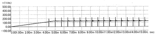
一方、起動用抵抗21には、FET3の動作状態にかかわらず、常に平滑コンデンサ1から放電電流が流れるので、起動用抵抗21による電力消費を低下させるために10MΩ以上の高抵抗値の抵抗が用いられる。従って、起動当初は、起動用コンデンサ12の充電速度も遅く、図10、図11に示すように、0.7乃至1.8msec程度のオフ期間が必然的に発生する間欠発振を繰り返す。
On the other hand, since a discharge current always flows from the
この自励式スイッチング電源回路100は、出力線20a、20bに流れる出力電流を監視する電流監視回路54と、出力線20a、20b間の出力電圧を監視する電圧監視回路55を有し、これらの監視値からトランス2の一次側で、出力電流と出力電圧を一定値である設定電流及び設定電圧以下に制御する出力制御回路56を備えている。
The self-excited switching power supply circuit 100 includes a
すなわち、出力制御回路56は、オフ期間中にトランス2の第2帰還巻線2dに発生するフライバック電圧で充電される駆動用コンデンサ37を備え、高圧側出力線20aと低圧側出力線20bに流れる出力電流若しくはこれらの間の出力電圧が設定電流若しくは設定電圧を越えると、フォトカプラ発光素子35が発光し、フォトカプラ発光素子35にフォトカップルするフォトカプラ受光素子36は、駆動用コンデンサ37からオフ制御トランジスタ5のベースへその受光量に比例した放電電流を流す。
That is, the
その結果、FET3がターンオンした後、一次巻線電流が流れることによる一次電流検出抵抗51に発生する電圧に、上記放電電流が電気抵抗52を流れることによる電圧がオフ制御トランジスタ5のベースに加わり、ベース電圧の上昇が加速される。これにより、オフ制御トランジスタ5は、速やかにオン動作してFET3がターンオフするので、オン時間が短縮され、出力電流若しくは出力電圧が低下して設定電流と設定電圧以下となることで定電流制御と定電圧制御が行われる。
As a result, after the
このうち設定電圧は、出力線20a、20b間に接続される負荷の動作電圧に設定され、設定電流は、自励式スイッチング電源回路100の各回路素子を保護するため、負荷が安定して動作する際の動作電流より高い値に設定される。
Among these, the set voltage is set to the operating voltage of the load connected between the
自励式スイッチング電源回路100の出力電流と出力電圧は、電源スイッチ4をONとしてスイッチ商用交流電源ACに接続した起動時から、上述したように間欠発振動作を繰り返しながら、出力電流が徐々に上昇し、図12のPS’で示すように、設定電流に達すると定電流制御下で徐々に出力電圧が上昇する。その後、出力電圧が負荷の動作電圧である設定電圧に達すると、定電圧制御化で出力電流が徐々に減少し、負荷の動作電流に達したときに、発振動作を繰り返しながら、負荷に見合った出力電圧と出力電流を安定出力する。
The output current and the output voltage of the self-excited switching power supply circuit 100 gradually increase from the start-up when the
この従来の自励式スイッチング電源回路100の出力線20a、20b間には、種々の負荷が接続されるが、モーターやDC−DCコンバータのような負荷は、安定動作するまでの動作電圧と動作電流が比例せず、例えば、図12にLで示すように、初期の動作電流が0.4A程度と高く、その後、動作電圧の上昇に伴って動作電流が緩やかに低下して、動作電圧5.5V、動作電流0.18A前後(図中S1)で安定動作を行う。
Various loads are connected between the
一方、自励式スイッチング電源回路100は、商用交流電源ACに接続した起動直後に間欠発振動作を繰り返すので、その出力特性は、図12のPS’で示すように、起動後の初期出力電流(短絡電流)が0.02A程度と低く、その後0.4V程度の出力電圧のまま出力電流が上昇する。従って、間欠発振動作を繰り返しながら、出力電流が上昇する図中S2において、その出力電圧と出力電流が、図中Lで示す負荷の動作特性に一致し、これを越えた電力を発生させる必要がないので、間欠発振動作の状態を繰り返す。その結果、自励式スイッチング電源回路100の出力は、負荷が安定動作する図中S1に達することがなく、いわゆる起動不良となる。 On the other hand, the self-excited switching power supply circuit 100 repeats the intermittent oscillation operation immediately after the start of connection to the commercial AC power supply AC. Current) is as low as about 0.02 A, and then the output current rises with an output voltage of about 0.4 V. Therefore, in S2 in the figure where the output current rises while repeating the intermittent oscillation operation, the output voltage and output current must match the operating characteristics of the load indicated by L in the figure, and it is necessary to generate power exceeding this. Since there is no, the state of intermittent oscillation operation is repeated. As a result, the output of the self-excited switching power supply circuit 100 does not reach S1 in FIG.
このような起動不良は、起動直後から起動用コンデンサ12の充電速度を上げて、間欠発振動作のオフ期間を短縮し、初期出力電流(短絡電流)を高くすることにより防止できるが、起動用抵抗21の抵抗値を下げる必要があり、抵抗値を下げた起動用抵抗21を用いると、負荷が接続されていない待機中であっても電流が流れることから待機消費電力が上昇してしまうという別の課題が生じる。
Such a startup failure can be prevented by increasing the charging speed of the
本発明は、このような従来の問題点を考慮してなされたものであり、高抵抗値の起動用抵抗を用いて待機消費電力を低下させたまま、起動直後から連続発振動作に移行し、起動不良が発生しない自励式スイッチング電源回路を提供することを目的とする。 The present invention has been made in consideration of such a conventional problem, and while transitioning to a continuous oscillation operation from immediately after startup while reducing standby power consumption using a high resistance startup resistor, It is an object of the present invention to provide a self-excited switching power supply circuit that does not cause a starting failure.
上述の目的を達成するため、請求項1に記載の自励式スイッチング電源回路は、高圧側端子と低圧側端子間に、商用交流電源を整流平滑化した直流入力電源を発生させる平滑コンデンサと、一次巻線と二次出力巻線と帰還巻線を有するトランスと、前記高圧側端子と低圧側端子間に、一次巻線と直列に接続された発振用電界効果トランジスタと、前記高圧側端子と発振用電界効果トランジスタのゲート間に接続された起動用抵抗と、一側が前記低圧側端子に接続する帰還巻線の他側と発振用電界効果トランジスタのゲート間に接続され、発振用電界効果トランジスタをオン制御する電圧をゲートへ印加する起動用コンデンサと、発振用電界効果トランジスタのゲートと前記低圧側端子間に接続され、発振用電界効果トランジスタがターンオンした所定時間後に、起動用コンデンサの充電電圧を放電し、発振用電界効果トランジスタをオフ制御する制御用スイッチング素子とを備え、発振用電界効果トランジスタがターンオフして二次出力巻線に発生するフライバック電圧を、整流平滑化して出力する自励式スイッチング電源回路において、前記高圧側端子と発振用電界効果トランジスタのゲートとの間に、起動用抵抗と並列にバイパス充電回路を接続し、バイパス充電回路は、直流入力電源の電圧が上昇する過渡期間の少なくとも一期間中に、前記高圧側端子から起動用コンデンサを充電する充電電流を流すことを最も主要な特徴とする。
In order to achieve the above-mentioned object, a self-excited switching power supply circuit according to
商用交流電源に接続した起動直後は、平滑コンデンサの充電電圧である直流入力電源の入力電圧は、0Vからピーク電圧まで上昇し、この0Vから上昇する過渡期間の少なくとも一期間に、起動用抵抗を介した充電路に加えて、バイパス充電回路を介した充電路で起動用コンデンサが充電される。その結果、高抵抗値の起動用抵抗を用いても、発振用電界効果トランジスタがターンオフしてから次にターンオンするまでのオフ期間が短縮され、過渡期間中であっても連続発振動作を行うので、起動直後に負荷の動作電流を上回る初期出力電流を出力し、起動不良が発生しない。 Immediately after start-up connected to the commercial AC power supply, the input voltage of the DC input power supply, which is the charging voltage of the smoothing capacitor, rises from 0 V to the peak voltage, and the start-up resistor is set at least during one of the transient periods rising from 0 V In addition to the charging path, the starting capacitor is charged in the charging path via the bypass charging circuit. As a result, even when a high-resistance start-up resistor is used, the off-period from when the oscillation field-effect transistor is turned off to when it is turned on is shortened, and continuous oscillation operation is performed even during the transient period. Immediately after startup, an initial output current exceeding the operating current of the load is output, and no startup failure occurs.
直流入力電源の電圧がピーク値に達するまでの過渡期間が経過した後の直流入力電源の電圧は、商用交流電源の半周期を周期としたリプル電圧が重畳する定常状態に移行し、定常状態に移行した後は、バイパス充電回路に流れる充電電流が停止するので、高抵抗値の起動用抵抗とすることにより、消費電力が低下する。 The voltage of the DC input power supply after the transition period until the voltage of the DC input power supply reaches the peak value transitions to a steady state in which a ripple voltage with a half cycle of the commercial AC power supply is superimposed, and enters the steady state. After the transition, the charging current flowing through the bypass charging circuit stops, so that the power consumption is reduced by using a high resistance starting resistor.
また、請求項2に記載の発明は、バイパス充電回路が、直列に接続した起動用補助抵抗と結合コンデンサとからなることを特徴とする。 According to a second aspect of the present invention, the bypass charging circuit includes a starting auxiliary resistor and a coupling capacitor connected in series.
起動用補助抵抗が直列に接続されることにより、結合コンデンサの充電電圧は、過渡期間に直流入力電源の入力電圧との間に電位差が生じ、結合コンデンサを充電する充電電流が直列に接続された起動用補助抵抗を介して起動用コンデンサに流れ、起動用コンデンサを補助充電する。 By connecting the starting auxiliary resistor in series, the charging voltage of the coupling capacitor has a potential difference with the input voltage of the DC input power supply during the transient period, and the charging current for charging the coupling capacitor is connected in series. It flows to the start capacitor via the start auxiliary resistor and auxiliary charge the start capacitor.
一方、直流入力電源の入力電圧が、定常状態でほぼ安定すると、結合コンデンサは飽和して、直流入力電源の電圧との電位差がなくなるので、起動用補助抵抗に充電電流が流れない。 On the other hand, when the input voltage of the DC input power supply is substantially stabilized in a steady state, the coupling capacitor is saturated and the potential difference from the voltage of the DC input power supply disappears, so that no charging current flows through the starting auxiliary resistor.
また、請求項3に記載の発明は、過渡期間が経過した後の直流入力電源の電圧よりツェナ電圧が低いツェナダイオードを、パイパス充電回路に直列に接続したことを特徴とする。
The invention described in
起動後に0Vから上昇する直流入力電源の電圧がツェナ電圧に達するまでは、結合コンデンサに充電電流が流れず、ツェナダイオードが結合コンデンサに直列に接続されることにより、過渡期間中の結合コンデンサの充電電圧と直流入力電源の電圧との電位差が減少する。その結果、パイパス充電回路から起動用コンデンサを充電する充電電流が減少するので、バイパス充電回路を設けることにより加速される起動用コンデンサの充電速度をツェナダイオードのツェナ電圧で遅らせることができる。 Charging current does not flow through the coupling capacitor until the voltage of the DC input power supply rising from 0V after startup reaches the Zener voltage, and the Zener diode is connected in series with the coupling capacitor, so that the coupling capacitor is charged during the transient period. The potential difference between the voltage and the voltage of the DC input power supply is reduced. As a result, since the charging current for charging the starting capacitor from the bypass charging circuit is reduced, the charging speed of the starting capacitor accelerated by providing the bypass charging circuit can be delayed by the Zener voltage of the Zener diode.
請求項1の発明によれば、高抵抗値の起動用抵抗を用いても、起動直後の直流入力電源の電圧が上昇する過渡期間に連続発振動作に移行させることができ、消費電力を増加させることなく、起動不良の発生を防止できる。 According to the first aspect of the present invention, even if a high-resistance startup resistor is used, it is possible to shift to a continuous oscillation operation during a transient period in which the voltage of the DC input power supply immediately after startup increases, thereby increasing power consumption. Therefore, it is possible to prevent the start-up failure.
請求項2の発明によれば、起動用補助抵抗と結合コンデンサを直列に接続する簡単な構成で、起動直後の過渡期間に起動用コンデンサを充電する充電電流が流れ、過渡期間が経過した後に、自然に充電電流が停止するバイパス充電回路を形成できる。
According to the invention of
請求項3の発明によれば、起動直後の起動用コンデンサの充電速度をツェナダイオードのツェナ電圧で任意に調整できるので、発振用電界効果トランジスタがターンオフしてからターンオンするまでのオフ期間を調整でき、トランスのエネルギー放出によって各巻線の極性が反転する前にターンオンし各回路素子に過大な逆電流が流れることを防止できる。
According to the invention of
以下、本発明の一実施の形態を図1乃至図7を用いて詳細に説明する。図1は、本発明の一実施の形態に係る自励式スイッチング電源回路10の構成を示す回路図である。本実施の形態に係る自励式スイッチング電源回路10は、図8で示した従来の自励式スイッチング電源回路100と主要な回路及び回路素子が共通するものであるので、同一の構成には同一の番号を付けて、その詳細な説明を省略する。 Hereinafter, an embodiment of the present invention will be described in detail with reference to FIGS. FIG. 1 is a circuit diagram showing a configuration of a self-excited switching power supply circuit 10 according to an embodiment of the present invention. The self-excited switching power supply circuit 10 according to the present embodiment has the same main circuit and circuit elements as the conventional self-excited switching power supply circuit 100 shown in FIG. The detailed description is omitted.
図1に示すように、自励式スイッチング電源回路10は、電源スイッチ4を介してブリッジ整流器7と平滑コンデンサ1からなるコンデンサインプット型整流平滑回路を100Vの商用交流電源ACに接続するもので、ピーク値が141Vの交流電圧をブリッジ整流器7で全波整流し、正弦波の半周期を繰り返す波形の電圧で平滑コンデンサ1を充電して平滑化し、平滑コンデンサ1の高圧側端子1aと低圧側端子1b間に発生するリプル電圧が重畳された直流電圧を、直流入力電源(以下、平滑コンデンサ1を単に直流入力電源といい、平滑コンデンサ1の充電電圧を入力電圧という)としている。従って、直流入力電源の入力電圧は、電源スイッチ4を閉じ、自励式スイッチング電源回路10が商用交流電源ACに接続した起動直後の0Vから141Vのピーク値に向かって上昇し(以下、商用交流電源ACに接続する前の電圧からピーク値まで上昇する期間を過渡期間という)、ピーク値に達すると、商用交流電源ACを全波整流した電圧波形により平滑コンデンサ1が充放電を繰り返し、ピーク値の近傍でリプル電圧波形が表れる定常状態に移行する。
As shown in FIG. 1, a self-excited switching power supply circuit 10 connects a capacitor input type rectifying / smoothing circuit comprising a bridge rectifier 7 and a smoothing
トランス2の一次巻線2aは、発振用電界効果型トランジスタ(以下、FETという)3と直列に、直流入力電源1に対して接続され、FET3のオンオフ動作によって、一次巻線2aに流れる電流がオンオフ制御される。FET3は、ここではMOSFETが用いられ、ドレインを一次巻線2aに接続し、ソースを一次電流検出抵抗51を介して直流入力電源1の低圧側端子1bに接続している。
The primary winding 2a of the
また、ゲートは、直流入力電源1に対して直列に接続された起動用抵抗21と電気抵抗25の接続点J1に、ゲートへの過大入力を阻止する電気抵抗24を介して接続している。起動用抵抗21と電気抵抗25のそれぞれの抵抗値は、図8に示す従来の回路と同様に、14.1MΩと750kΩであり、これにより141V前後の不安定な直流入力電源1が起動用抵抗21と電気抵抗25の両端に加わえられても、起動用抵抗21には約9.5μAの微弱な電流が流れるだけであり、起動用抵抗21による電力消費を著しく低下させることができる。
Further, the gate is connected to a connection point J1 of the starting
起動用抵抗21と電気抵抗25の接続点J1と、第1帰還巻線2bの間には、FET3のオン動作に作用する起動用コンデンサ12及び帰還抵抗11が直列に接続され、第1帰還巻線2bの他側は、直流入力電源1の低圧側端子1bに接続している。
A starting
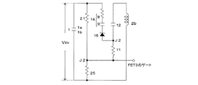
本実施の形態では、従来の回路と異なり、図2に示すように、この起動用コンデンサ12と帰還抵抗11の接続点J2と直流入力電源1の高圧側端子1a間に、バイパス充電回路14を構成する起動用補助抵抗8及び結合コンデンサ9と、ツェナダイオード15を直列に接続している。
In the present embodiment, unlike the conventional circuit, as shown in FIG. 2, a bypass charging circuit 14 is provided between the connection point J2 of the starting
ここで、起動用補助抵抗8の抵抗値は、470kΩ、結合コンデンサ9の容量は0.0047μFとして、結合コンデンサ9が飽和するまでの時間を、後述するように、起動後過渡期間が経過するまでの5msecより長い14msec前後としている(図3参照)。 Here, the resistance value of the starting auxiliary resistor 8 is 470 kΩ, the capacitance of the coupling capacitor 9 is 0.0047 μF, and the time until the coupling capacitor 9 is saturated until the transient period after startup elapses as will be described later. 14 msec, which is longer than 5 msec (see FIG. 3).
また、ツェナダイオード15は、カソードを高圧側端子1a側のバイパス充電回路14に、アノードを接続点J2に接続し、これにより直流入力電源1の電圧がツェナダイオード15のツェナ電圧に達するまでは、過渡期間中であってもバイパス充電回路14に充電電流が流れないようにしている。従って、ツェナ電圧は、少なくとも141Vのピーク値より低く、ここでは、ツェナ電圧が39Vのツェナダイオード15を用いている。
Further, the
起動用抵抗21と電気抵抗25の接続点J1と低圧側端子1b間には、FET3のゲート電圧を低下させてオフ制御するスイッチング素子であるオフ制御トランジスタ5が配置されている。ここでは、オフ制御トランジスタ5として、コレクタを接続点J1へ、エミッタを低圧側端子1bへ接続させたNPN型トランジスタを用いている。オフ制御トランジスタ5のベースは、オフ制御用コンデンサ53を介して低圧側端子1bに接続するとともに、電気抵抗52を介して一次電流検出抵抗51の高圧側に接続し、一次電流検出抵抗51による電圧降下が一定値以上となると、オフ制御用コンデンサ53の充電電圧で表されるベース電圧が上昇し、オフ制御トランジスタ5がオン動作するようになっている。
Between the connection point J1 of the starting
第2帰還巻線2dの一側は、直列に接続された整流ダイオード54と駆動用コンデンサ37を介して直流入力電源1の低圧側端子1bに接続し、また他側は、直接直流入力電源1の低圧側端子1bに接続し、これにより閉ループが形成される。整流ダイオード54は、駆動用コンデンサ37との接続方向を順方向として配設され、第2帰還巻線2dに発生するフライバック電圧で駆動用コンデンサ37が充電されるようになっている。整流ダイオード54と駆動用コンデンサ37の接続点は、フォトカプラ受光素子36を介してオフ制御トランジスタ5のベースへ接続している。
One side of the second feedback winding 2d is connected to the low-
フォトカプラ受光素子36は、トランス2の二次側のフォトカプラ発光素子35とフォトカップルして動作するもので、フォトカプラ発光素子35からの光を受光している間に、駆動用コンデンサ37から放電される放電電流をその受光量に比例して流す。
The photocoupler light-receiving
トランスの二次出力巻線2cには、二次出力巻線2cと直列に整流用ダイオードと、二次出力巻線2cと並列に平滑コンデンサとからなる出力側整流平滑回路26が接続している。
Connected to the secondary output winding 2c of the transformer is an output side rectifying / smoothing
出力電圧監視回路55は、高圧側出力線20aと低圧側出力線20b間の出力電圧が所定の値に設定した設定電圧となったときに、直列に接続された分圧抵抗30、31の分圧抵抗31による電圧降下が、NPNトランジスタ32が能動状態で動作するように、分圧抵抗30、31の各抵抗値が定められている。従って、出力電圧が設定電圧を超えると、その差電圧に比例する電流がフォトカプラ発光素子35に流れ、フォトカプラ発光素子35は、差電圧に応じた発光量で発光する。
When the output voltage between the high voltage
出力電流監視回路54は、低圧側出力線20bにシャント抵抗33が直列に接続され、シャント抵抗33に流れる出力電流が所定の値に設定した設定電流となったときに、シャント抵抗33による電圧降下で、NPNトランジスタ34が能動状態で動作するように定められている。従って、出力電流が設定電流を超えると、その差電流に比例する電流がフォトカプラ発光素子35に流れ、フォトカプラ発光素子35は、差電流に応じた発光量で発光する。
The output
フォトカプラ発光素子35は、前述したようにトランス2の一次側のフォトカプラ受光素子36とフォトカップリングしている。その結果、出力電流が設定電流を越え、若しくは出力電圧が設定電圧を超えると、FET3のオン期間中に、ターンオン前に充電されていた駆動用コンデンサ37から、その超えた値に応じた放電電流を電気抵抗52と一次電流検出抵抗51へ流す。電気抵抗52に放電電流が流れることにより、オフ制御用コンデンサ53の充電が加速され、オフ制御用コンデンサ53が速やかにオン動作することによりFET3のオン期間が短縮される。その結果、オン期間中にトランス2に蓄積されるエネルギーが減少し、設定値を超えていた出力電圧若しくは出力電流は設定電圧若しくは設定電流となるように制御される。
The photocoupler light-emitting
以下、このように構成された自励式スイッチング電源回路10の動作を、特に電源スイッチ4を閉じ操作し、商用交流電源ACに接続させた起動直後の動作を中心に説明する。電源スイッチ4をONとして商用交流電源ACに接続すると、ブリッジ整流回路7で整流された正弦波の半周期を繰り返す正弦波電圧により平滑コンデンサ1が充電される。平滑コンデンサ1に接続される抵抗成分を無視すれば、高圧側端子1aと低圧側端子1b間に、図9に示すように、0Vから141Vに向かって上昇する正弦波形の直流入力電源の入力電圧VINが表れる。
Hereinafter, the operation of the self-excited switching power supply circuit 10 configured as described above will be described with a focus on the operation immediately after startup, particularly when the
直流入力電源1の入力電圧VINが上昇する過渡期間には、直流入力電源1から起動用抵抗21を介して起動用コンデンサ12が充電される(図中下の電極が+で上が−の極性)。このとき、起動用コンデンサ12と帰還抵抗11の接続点J2と直流入力電源1の高圧側端子1a間にも直流入力電源1の入力電圧VINが加わるが、ツェナダイオード15のツェナ電圧(39V)に達するまでは、この間に電流が流れない。つまり、図3に示すように、直流入力電源1の入力電圧VINが0Vから39Vのツェナ電圧に達するまでの結合コンデンサ9の両端の充電電圧VCは、直流入力電源1の入力電圧VINに一致し、起動用コンデンサ12は、起動用抵抗21に流れる充電電流のみで充電される。
During the transition period in which the input voltage VIN of the DC
起動用コンデンサ12の充電電圧が徐々に上昇し、その充電電圧がFET3のスレッショルド電圧VTHに達すると、FET3のゲートに順方向バイアス電圧が印加され、FET3がターンオンする(ドレイン−ソース間が導通する)。FET3がターンオンし、直列に接続された一次巻線2aに直流入力電源1から励磁電流が流れ始めると、トランス2の各巻線に誘導起電力が生じ、トランス2にエネルギーが蓄積される。帰還巻線2bに発生する誘起電圧は、起動用コンデンサ12の充電電圧と重畳し、FET3のゲート電圧をそのスレッショルド電圧VTH以上の電圧(オン電圧)に維持する。
Starting ramping the charging voltage of the
FET3がオン動作しているオン期間中は、励磁電流が流れることによる一次電流検出抵抗51の両端の電圧で、オフ制御用コンデンサ53が充電され、ターンオン後の経過時に比例して上昇する励磁電流に伴って、オフ制御用コンデンサ53の充電電圧も上昇する。その充電電圧がオフ制御トランジスタ5のバイアス電圧に達すると、コレクタ−エミッタ間が導通状態になり、FET3のゲートはオフ制御トランジスタ5によって実質的に短絡状態となり、FET3がターンオフする。
During the ON period in which the
FET3のターンオフに伴って、各巻線には、いわゆるフライバック電圧(誘導逆起電力)が発生するが、平滑コンデンサ1への充電が進む過渡期間中、とりわけ、その初期段階では、直流入力電源1の入力電圧VINが十分に上昇していないため、トランス2に蓄積されるエネルギーが少なく、フライバック電圧の電圧値が小さい。従って、この期間では、帰還巻線2bのフライバック電圧による起動用コンデンサ12への充電が十分に行われない。
As the
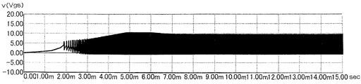
その一方で、平滑コンデンサ1への充電が進む過渡期間中に、直流入力電源1の入力電圧VINがツェナダイオード15のツェナ電圧(39V)を越えると、図3に示すように、結合コンデンサ9の両端の充電電圧VCと直流入力電源1の入力電圧VIN間に電位差が発生し、起動用補助抵抗8に結合コンデンサ9を充電しようとする充電電流が流れ始める。この充電電流は、高圧側端子1aから接続点J2の方向に流れるので、起動用コンデンサ12は、起動用抵抗21に流れる充電電流に、起動用補助抵抗8と結合コンデンサ9とからなるバイパス充電回路14に流れる充電電流が加わり充電される。その結果、FET3がターンオフ後にターンオンするまでのオフ期間が短縮され、この発振動作を繰り返すことにより、自励式スイッチング電源回路10は、従来の自励式スイッチング電源回路10の間欠発振動作(図9乃至図11参照)と異なり、図4乃至図6に示すように連続発振動作を行う。
On the other hand, when the input voltage VIN of the DC
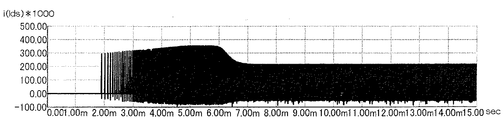
図4、図6に示すように、自励式スイッチング電源回路10は、起動直後の直流入力電源1の入力電圧VINが上昇する過渡期間中に連続発振動作に移行するので、図7の電源回路10の出力特性PSに示すように、起動後の初期出力電流(短絡電流)が0.5A以上となり、動作特性Lで初期の動作電流が0.4A程度の負荷が出力線20a、20b間に接続されていても、起動中の出力特性PSが動作特性Lに一致することなく、起動不良は発生しない。
As shown in FIGS. 4 and 6, the self-excited switching power supply circuit 10 shifts to a continuous oscillation operation during a transient period in which the input voltage VIN of the DC
平滑コンデンサ1への充電が進み、直流入力電源1の入力電圧VINが上昇した状態において、自励式スイッチング電源回路10が連続発振動作を行っている各発振周期のオフ期間は、トランス2に流れる電流が実質的に遮断され、各巻線には前述の通りフライバック電圧が生じ、二次出力巻線2cに発生するフライバック電圧は、出力側整流平滑回路26によって整流平滑化され、出力線20a、20b間に接続される負荷に供給される電力として出力される。また、第1帰還巻線2bに発生するフライバック電圧は、出力側に接続された負荷により二次巻線2cに発生するフライバック電圧と比例関係にあり、この第1帰還巻線2bに発生するフライバック電圧によっても、ツェナダイオード6を介して起動用コンデンサ12が充電される。充電過渡期間中の入力電圧VINの上昇に伴って、このフライバック電圧による起動用コンデンサ12への充電電流が次第に大きくなり、起動用コンデンサ12の充電は更に加速され、図4乃至図6に示すように、オフ期間が徐々に短縮される。
When the smoothing
連続発振する自励式スイッチング電源回路10は、起動後の0.5A以上の初期出力電流から出力電流が上昇し、設定電流を越えると、上述の通り、設定電流との差電流に応じて駆動用コンデンサ37の放電電流が電気抵抗52に流れ、オフ制御用コンデンサ53の充電が加速されてFET3のオン時間が短縮されることにより設定電流に定電流制御される。図7に示すように、定電流制御下で出力電圧は徐々に上昇し、設定電圧を超えると、電圧監視回路55が設定電圧との差電圧を検出し、同様に、差電圧に応じてFET3のオン時間が短縮される定電圧制御が行われる。ここでは、設定電圧を、接続される負荷の通常の動作電圧に設定し、定電圧制御下では、各発振周期毎にトランス2に蓄積されるエネルギーを負荷が消費し、フライバック電圧が低下するまで、起動用コンデンサ12の充電電圧では、FET3のゲート電圧をそのスレッショルド電圧VTH以上の電圧としないので、ターンオンが徐々に遅れ、出力電流が低下し、負荷の通常の動作電流に出力電流が一致しするS1(ここでは、出力電圧が5.5V、出力電流が約0.18A)で負荷のエネルギー消費に見合った安定した連続発振動作を繰り返す。
The self-excited switching power supply circuit 10 that continuously oscillates is driven according to the difference current from the set current as described above when the output current rises from the initial output current of 0.5 A or more after startup and exceeds the set current. The discharge current of the
本実施の形態では、図3に示すように、結合コンデンサ9の過渡期間が直流入力電源1の入力電圧VINの過渡期間、すなわち平滑コンデンサ1の過渡期間より長い時間となるように時定数が設定され、従って、入力電圧VINがピーク値(141V)に達する定常状態に移行した後、結合コンデンサ9の充電電圧VCは入力電圧VINに達し、バイパス充電回路14に流れる充電電流が停止する。その結果、定常状態で安定した連続発振動作に移行した後は、オフ期間中に起動用コンデンサ12は起動用抵抗21を介した入力電圧VINと第1帰還巻線2bに発生するフライバック電圧のみにより充電され、高抵抗値の起動用抵抗21を用いることにより、連続発振動作中や負荷が接続されていない待機期間中の電力消費を低減させることができる。
In the present embodiment, as shown in FIG. 3, the time constant is set so that the transient period of the coupling capacitor 9 is longer than the transient period of the input voltage VIN of the DC
このように入力電圧VINが上昇する過渡期間にバイパス充電回路14に流れる充電電流で起動用コンデンサ12の充電速度を加速させ、オフ期間を短縮させる本発明では、起動不良を防止できるが、一方、トランス2の二次側にフライバック電圧が残り、一次巻線2aに直流入力電源1と逆極性のフライバック電圧が発生している間であっても、FET3のゲート電圧がスレッショルド電圧VTHに達してターンオンし、ターンオンした際に過大な電流が発生して回路素子を破損させるという新た問題が発生する恐れが生じた。そこで、本実施の形態では、バイパス充電回路14に直列にツェナダイオード15を接続し、入力入力電圧VINがツェナ電圧に達した後に、バイパス充電回路14に充電電流を流すようにしている。つまり、ツェナダイオード15を接続することにより、図3に示す起動直後から充電電流が流れるまでの時間が延長され、また、入力電圧VINと結合コンデンサ9の充電電圧VCの差電圧、すなわち、起動用補助抵抗8を流れる充電電流を減少させることができるので、ツェナダイオード15のツェナ電圧で起動用コンデンサ12の充電速度を調整することができ、確実にフライバック電圧が消失した後にFET3がターンオンするようにオフ期間を調整できる。
As described above, in the present invention in which the charging speed of the starting
一方、接続する負荷によって、上記問題が生じる可能性がない場合には、ツェナダイオード15を接続せずに、起動直後の入力電圧VINが0Vであるときから、バイパス充電回路14に流れる充電電流で起動用コンデンサ12を充電し、より早期に連続発振動作に移行させてもよい。
On the other hand, if there is no possibility that the above problem occurs due to the load to be connected, the charging current flowing in the bypass charging circuit 14 from when the input voltage VIN immediately after startup is 0 V without connecting the
また、相互に直列に接続される起動用補助抵抗8、結合コンデンサ9及びツェナダイオード15の接続順は、ツェナダイオード15のカソードを直流入力電源1の高圧側端子1a側に接続するものであれば、上記実施の形態にかかわらず任意である。
The starting auxiliary resistor 8, the coupling capacitor 9 and the
本発明は、商用交流電源ACに接続するコンデンサインプット型のスイッチング電源回路に適している。 The present invention is suitable for a capacitor input type switching power supply circuit connected to a commercial AC power supply AC.
1 直流入力電源(平滑コンデンサ)
1a 高圧側端子
1b 低圧側端子
2 トランス
2a 一次巻線
2b 帰還巻線(第1帰還巻線)
2c 二次出力巻線
3 発振用電界効果トランジスタ
5 オフ制御トランジスタ(制御用スイッチング素子)
8 起動用補助抵抗
9 結合コンデンサ
10 自励式スイッチング電源回路
12 起動用コンデンサ
14 バイパス充電回路
15 ツェナダイオード
21 起動用抵抗
1 DC input power supply (smoothing capacitor)
1a High-
2c Secondary output winding 3 Oscillation
8 Auxiliary resistance for starting 9 Coupling capacitor 10 Self-excited switching
Claims (3)
一次巻線と二次出力巻線と帰還巻線を有するトランスと、
前記高圧側端子と低圧側端子間に、一次巻線と直列に接続された発振用電界効果トランジスタと、
前記高圧側端子と発振用電界効果トランジスタのゲート間に接続された起動用抵抗と、
一側が前記低圧側端子に接続する帰還巻線の他側と発振用電界効果トランジスタのゲート間に接続され、発振用電界効果トランジスタをオン制御する電圧をゲートへ印加する起動用コンデンサと、
発振用電界効果トランジスタのゲートと前記低圧側端子間に接続され、発振用電界効果トランジスタがターンオンした所定時間後に、起動用コンデンサの充電電圧を放電し、発振用電界効果トランジスタをオフ制御する制御用スイッチング素子とを備え、
発振用電界効果トランジスタがターンオフして二次出力巻線に発生するフライバック電圧を、整流平滑化して出力する自励式スイッチング電源回路において、
前記高圧側端子と発振用電界効果トランジスタのゲートとの間に、起動用抵抗と並列にバイパス充電回路を接続し、
バイパス充電回路は、直流入力電源の電圧が上昇する過渡期間の少なくとも一期間中に、前記高圧側端子から起動用コンデンサを充電する充電電流を流すことを特徴とする自励式スイッチング電源回路。 A smoothing capacitor for generating a DC input power source obtained by rectifying and smoothing a commercial AC power source between a high voltage side terminal and a low voltage side terminal;
A transformer having a primary winding, a secondary output winding and a feedback winding;
An oscillation field effect transistor connected in series with the primary winding between the high-voltage side terminal and the low-voltage side terminal;
A starting resistor connected between the high-voltage side terminal and the gate of the oscillation field effect transistor;
A starting capacitor that is connected between the other side of the feedback winding connected to the low-voltage side terminal and the gate of the oscillation field-effect transistor, and that applies a voltage for on-controlling the oscillation field-effect transistor to the gate;
Connected between the gate of the oscillation field effect transistor and the low-voltage side terminal, and after a predetermined time when the oscillation field effect transistor is turned on, the charging voltage of the starting capacitor is discharged and the oscillation field effect transistor is turned off. A switching element,
In the self-excited switching power supply circuit that outputs the rectified and smoothed flyback voltage generated in the secondary output winding by turning off the oscillation field effect transistor,
Between the high-voltage side terminal and the gate of the oscillation field effect transistor, a bypass charging circuit is connected in parallel with the starting resistor,
The bypass charging circuit is a self-excited switching power supply circuit characterized in that a charging current for charging the starting capacitor flows from the high-voltage side terminal during at least one transitional period in which the voltage of the DC input power supply rises.
Priority Applications (4)
| Application Number | Priority Date | Filing Date | Title |
|---|---|---|---|
| JP2011054258A JP5408161B2 (en) | 2011-03-11 | 2011-03-11 | Self-excited switching power supply circuit |
| US13/413,661 US8437151B2 (en) | 2011-03-11 | 2012-03-07 | Self-excited switching power supply circuit |
| CN201210061952.5A CN102723875B (en) | 2011-03-11 | 2012-03-09 | Self-excited switching power supply circuit |
| EP12158723A EP2498389A2 (en) | 2011-03-11 | 2012-03-09 | Self-excited switching power supply circuit |
Applications Claiming Priority (1)
| Application Number | Priority Date | Filing Date | Title |
|---|---|---|---|
| JP2011054258A JP5408161B2 (en) | 2011-03-11 | 2011-03-11 | Self-excited switching power supply circuit |
Publications (2)
| Publication Number | Publication Date |
|---|---|
| JP2012191794A true JP2012191794A (en) | 2012-10-04 |
| JP5408161B2 JP5408161B2 (en) | 2014-02-05 |
Family
ID=45976659
Family Applications (1)
| Application Number | Title | Priority Date | Filing Date |
|---|---|---|---|
| JP2011054258A Expired - Fee Related JP5408161B2 (en) | 2011-03-11 | 2011-03-11 | Self-excited switching power supply circuit |
Country Status (4)
| Country | Link |
|---|---|
| US (1) | US8437151B2 (en) |
| EP (1) | EP2498389A2 (en) |
| JP (1) | JP5408161B2 (en) |
| CN (1) | CN102723875B (en) |
Families Citing this family (5)
| Publication number | Priority date | Publication date | Assignee | Title |
|---|---|---|---|---|
| CN103458559B (en) * | 2012-06-04 | 2015-04-15 | 欧普照明股份有限公司 | Drive system of semiconductor light source and semiconductor illumination device |
| CN103199692A (en) * | 2013-03-14 | 2013-07-10 | 中国科学院微电子研究所 | Monolithic low power consumption starting circuit device arranged inside chip and used in switching power supply |
| JP2019047621A (en) * | 2017-09-01 | 2019-03-22 | ミツミ電機株式会社 | Semiconductor device for power supply control, power supply device, and discharge method of x capacitor |
| CN107505488B (en) * | 2017-10-13 | 2019-10-08 | 国网湖南省电力公司 | Lightning surge generator and its control method for arrester heavy-current discharge counter |
| DE202018000753U1 (en) * | 2018-02-14 | 2019-05-16 | Matrix Industries, Inc. | Starting circuit for energy harvesting circuits |
Citations (4)
| Publication number | Priority date | Publication date | Assignee | Title |
|---|---|---|---|---|
| JPH02131366A (en) * | 1988-11-08 | 1990-05-21 | Mitsubishi Electric Corp | Switching regulator |
| JP2005006477A (en) * | 2003-06-16 | 2005-01-06 | Smk Corp | Self-excitation type switching power supply circuit |
| JP2009219218A (en) * | 2008-03-10 | 2009-09-24 | Panasonic Corp | Switching apparatus |
| JP2011035988A (en) * | 2009-07-30 | 2011-02-17 | Aiphone Co Ltd | Switching power supply unit |
Family Cites Families (5)
| Publication number | Priority date | Publication date | Assignee | Title |
|---|---|---|---|---|
| JP3155715B2 (en) * | 1996-09-27 | 2001-04-16 | 東光株式会社 | Self-excited switching power supply circuit |
| JP3351464B2 (en) * | 1998-02-13 | 2002-11-25 | 株式会社村田製作所 | Self-oscillation type switching power supply |
| JP3675389B2 (en) * | 2001-03-26 | 2005-07-27 | 株式会社村田製作所 | Switching power supply device and electronic device using the same |
| JP3691479B2 (en) | 2002-11-25 | 2005-09-07 | 三洋電機株式会社 | Heart rate / respiration measurement device |
| CN100461603C (en) * | 2006-09-05 | 2009-02-11 | 广州金升阳科技有限公司 | Isolated self-oscillation reverse exciting inverter |
-
2011
- 2011-03-11 JP JP2011054258A patent/JP5408161B2/en not_active Expired - Fee Related
-
2012
- 2012-03-07 US US13/413,661 patent/US8437151B2/en not_active Expired - Fee Related
- 2012-03-09 EP EP12158723A patent/EP2498389A2/en not_active Withdrawn
- 2012-03-09 CN CN201210061952.5A patent/CN102723875B/en not_active Expired - Fee Related
Patent Citations (4)
| Publication number | Priority date | Publication date | Assignee | Title |
|---|---|---|---|---|
| JPH02131366A (en) * | 1988-11-08 | 1990-05-21 | Mitsubishi Electric Corp | Switching regulator |
| JP2005006477A (en) * | 2003-06-16 | 2005-01-06 | Smk Corp | Self-excitation type switching power supply circuit |
| JP2009219218A (en) * | 2008-03-10 | 2009-09-24 | Panasonic Corp | Switching apparatus |
| JP2011035988A (en) * | 2009-07-30 | 2011-02-17 | Aiphone Co Ltd | Switching power supply unit |
Also Published As
| Publication number | Publication date |
|---|---|
| JP5408161B2 (en) | 2014-02-05 |
| CN102723875B (en) | 2015-02-04 |
| CN102723875A (en) | 2012-10-10 |
| US20120230061A1 (en) | 2012-09-13 |
| US8437151B2 (en) | 2013-05-07 |
| EP2498389A2 (en) | 2012-09-12 |
Similar Documents
| Publication | Publication Date | Title |
|---|---|---|
| US10158282B1 (en) | Switching power supply device | |
| KR101168588B1 (en) | Power supply apparatus and image forming apparatus | |
| US9331583B2 (en) | Switch mode power supply, control circuit and associated control method | |
| JP3707436B2 (en) | Switching power supply | |
| JP4481879B2 (en) | Switching power supply | |
| US9787204B2 (en) | Switching power supply device | |
| US6178100B1 (en) | Switching power source | |
| JP4787350B2 (en) | Self-excited switching power supply circuit | |
| JP2006129548A (en) | Power converter | |
| JP6840032B2 (en) | Insulated switching power supply | |
| JP5408161B2 (en) | Self-excited switching power supply circuit | |
| JP3760379B2 (en) | Switching power supply | |
| US8582320B2 (en) | Self-excited switching power supply circuit | |
| US9490717B2 (en) | Switching power supply circuit | |
| JP3691498B2 (en) | Self-excited switching power supply circuit | |
| US9564819B2 (en) | Switching power supply circuit | |
| JP4339030B2 (en) | Self-excited switching power supply circuit oscillation control method | |
| JP4329113B2 (en) | Switching power supply | |
| JP2004015993A (en) | Power saving power supply under no load | |
| JP4484006B2 (en) | Switching power supply | |
| JP6942040B2 (en) | Insulated switching power supply | |
| JP2008193803A (en) | Switching power supply device | |
| JP2015128372A (en) | Power supply device and image forming apparatus | |
| JP2012138984A (en) | Ringing choke converter | |
| JP2013102689A (en) | Power supply device and image forming apparatus |
Legal Events
| Date | Code | Title | Description |
|---|---|---|---|
| A711 | Notification of change in applicant |
Free format text: JAPANESE INTERMEDIATE CODE: A711 Effective date: 20120713 |
|
| A521 | Request for written amendment filed |
Free format text: JAPANESE INTERMEDIATE CODE: A821 Effective date: 20120713 |
|
| A977 | Report on retrieval |
Free format text: JAPANESE INTERMEDIATE CODE: A971007 Effective date: 20130206 |
|
| A131 | Notification of reasons for refusal |
Free format text: JAPANESE INTERMEDIATE CODE: A131 Effective date: 20130312 |
|
| TRDD | Decision of grant or rejection written | ||
| A01 | Written decision to grant a patent or to grant a registration (utility model) |
Free format text: JAPANESE INTERMEDIATE CODE: A01 Effective date: 20131008 |
|
| A61 | First payment of annual fees (during grant procedure) |
Free format text: JAPANESE INTERMEDIATE CODE: A61 Effective date: 20131021 |
|
| R150 | Certificate of patent or registration of utility model |
Ref document number: 5408161 Country of ref document: JP Free format text: JAPANESE INTERMEDIATE CODE: R150 |
|
| LAPS | Cancellation because of no payment of annual fees |