JP2012191299A - Piezoelectric vibration element, piezoelectric vibrator, piezoelectric oscillator, and electronic device - Google Patents
Piezoelectric vibration element, piezoelectric vibrator, piezoelectric oscillator, and electronic device Download PDFInfo
- Publication number
- JP2012191299A JP2012191299A JP2011051311A JP2011051311A JP2012191299A JP 2012191299 A JP2012191299 A JP 2012191299A JP 2011051311 A JP2011051311 A JP 2011051311A JP 2011051311 A JP2011051311 A JP 2011051311A JP 2012191299 A JP2012191299 A JP 2012191299A
- Authority
- JP
- Japan
- Prior art keywords
- piezoelectric
- axis
- vibration element
- excitation
- piezoelectric vibration
- Prior art date
- Legal status (The legal status is an assumption and is not a legal conclusion. Google has not performed a legal analysis and makes no representation as to the accuracy of the status listed.)
- Granted
Links
Images


Abstract
Description
本発明は、厚み振動モードの圧電振動子に関し、特に所謂メサ型の構造を有する圧電振動素子、圧電振動子、圧電発振器及び電子デバイスに関する。 The present invention relates to a thickness vibration mode piezoelectric vibrator, and more particularly to a piezoelectric vibration element, a piezoelectric vibrator, a piezoelectric oscillator, and an electronic device having a so-called mesa structure.
ATカット水晶振動素子を用いた水晶振動素子は、その振動モードが厚みすべり振動であり、且つ周波数温度特性が優れた三次曲線を呈するので、電子機器等の多方面で使用されている。
特許文献1には、エネルギー閉じ込め効果が、ベベル構造やコンベックス構造と同程度の効果を有する、所謂、メサ型構造の圧電振動子(ATカット水晶振動子)が開示されている。
辺比(厚さに対する辺の長さの比)の小さな厚みすべり振動子は、辺比が適切に設定されないと、圧電基板の輪郭寸法に起因する輪郭振動(屈曲振動等)が主振動に結合し、主振動の特性を劣化させることが知られている。
特許文献2には、ATカット水晶振動子をメサ型構造で形成し、メサ部と薄肉部との境界の境界において、境界部の側壁が主面に対して90°であると励振電極から延出された引き出し電極(リード電極)が断線してしまうという問題に鑑みてなされたものであって、前記境界部の側壁を傾斜または曲面とすることにより、前記リード電極の断線を防止することができることが開示されている。また、振動部分の表面のあらさを、平均粗さで0.2ミクロンと小さな表面粗さとすることにより、CI値が低下し、副振動が抑圧されると開示されている。
また、特許文献3には、ATカット水晶振動子をメサ型構造で形成し、メサ部の側壁を、63°、35°と傾斜させて、厚みすべり振動と屈曲振動との結合を抑圧した水晶振動子が開示されている。
A crystal resonator element using an AT-cut crystal resonator element is used in various fields such as electronic equipment because its vibration mode is a thickness-shear vibration and exhibits a cubic curve having excellent frequency temperature characteristics.
If the side ratio (ratio of the length of the side to the thickness) is small, if the side ratio is not set appropriately, contour vibrations (bending vibration, etc.) due to the contour dimensions of the piezoelectric substrate will be coupled to the main vibration. However, it is known to deteriorate the characteristics of the main vibration.
In
Patent Document 3 discloses a crystal in which an AT-cut quartz crystal resonator is formed with a mesa structure, and the side wall of the mesa portion is inclined at 63 ° and 35 ° to suppress the coupling between thickness shear vibration and bending vibration. An oscillator is disclosed.
特許文献4には、水晶振動素子の周波数をf、水晶基板の長辺(X軸)の長さをX、メサ部(振動部)の厚みをt、メサ部の長辺の長さをMx、励振電極の長辺の長さをEx、水晶基板の長辺方向に生じる屈曲振動の波長をλとするとき、以下の4つの式、
λ/2=(1.332/f)−0.0024 (1)
(Mx−Ex)/2=λ/2 (2)
Mx/2=(n/2+1/4)λ(但しnは整数) (3)
X≧20t (4)
を満たすように各パラメータf、X、Mx、Exを設定することにより、厚みすべり振動と屈曲振動との結合を抑制できると開示されている。
In Patent Document 4, the frequency of the quartz resonator element is f, the length of the long side (X axis) of the quartz substrate is X, the thickness of the mesa portion (vibrating portion) is t, and the length of the long side of the mesa portion is Mx. When the length of the long side of the excitation electrode is Ex and the wavelength of the bending vibration generated in the long side direction of the quartz substrate is λ, the following four formulas:
λ / 2 = (1.332 / f) −0.0024 (1)
(Mx−Ex) / 2 = λ / 2 (2)
Mx / 2 = (n / 2 + 1/4) λ (where n is an integer) (3)
X ≧ 20t (4)
It is disclosed that the coupling between the thickness shear vibration and the bending vibration can be suppressed by setting the parameters f, X, Mx, and Ex so as to satisfy the above.
特許文献5には、メサ型構造の圧電基板のメサ部の高さ(段差部の堀量)yは、圧電基板の長辺の寸法をx、メサ部(振動部)の厚み寸法をtとした時に、板厚tを基準として、次式
y=−0.89×(x/t)+34±3(%)
を満たすように辺比を設定することにより、不要モードを抑圧できると開示されている。
特許文献6には、メサ型構造の圧電基板の短辺の長さをZとし、メサ部(振動部)の厚みをtとし、メサ部の短辺方向の電極寸法をMzとしたときに、
15.68≦Z/t≦15.84、かつ、0.77≦Mz/Z≦0.82
の関係を満たすように諸パラメータを設定することにより、不要モードを抑圧できると開示されている。
In
It is disclosed that the unnecessary mode can be suppressed by setting the side ratio to satisfy the above.
In Patent Document 6, when the length of the short side of the mesa-type piezoelectric substrate is Z, the thickness of the mesa part (vibration part) is t, and the electrode dimension in the short side direction of the mesa part is Mz,
15.68 ≦ Z / t ≦ 15.84 and 0.77 ≦ Mz / Z ≦ 0.82
It is disclosed that the unnecessary mode can be suppressed by setting various parameters so as to satisfy the above relationship.
しかし、更に辺比の小さな圧電振動子では、振動変位がX軸の端部で十分には減衰せずに、端面で不要な屈曲モードなどを励起し、これが主振動と結合するという課題があった。
特許文献7には、メサ構造を多段とすることにより、主振動の振動エネルギーをより完全に閉じ込めることが可能になる旨が開示されている。
特許文献8には、断面形状がコンベックス形状の圧電基板を、想定するコンベックス形状の包絡線に沿って階段形状に構成することにより、近似的に置き換えが可能であり、さらに、階段状の側面を斜面とすればより近似度合いが増すと開示されている。
However, in the piezoelectric vibrator having a smaller side ratio, the vibration displacement is not sufficiently attenuated at the end of the X axis, and an unnecessary bending mode is excited at the end face, which is coupled with the main vibration. It was.
Patent Document 7 discloses that the vibration energy of the main vibration can be more completely confined by using a multi-stage mesa structure.
In Patent Document 8, a piezoelectric substrate having a convex cross-sectional shape can be approximately replaced by constructing a stepped shape along an assumed convex-shaped envelope. It is disclosed that the degree of approximation increases if it is a slope.
特許文献9、特許文献10には、メサ型構造の圧電基板のメサ部を多段とすることにより、主振動のエネルギー閉じ込め効果を高め、不要モードを抑圧することができると開示されている。
特許文献11には、メサ型構造の段差部を導電性接着剤の流れ止めとし、メサ部への接着剤の流入防止を図ったメサ型振動デバイスが開示されている。このように、特許文献7乃至特許文献11には、圧電基板のメサ構造を多段メサ構造とし、エネルギー閉じ込めを深くすることが、主振動と屈曲振動との結合の抑圧に有用であると開示されている。
Patent Document 9 and
最近の小型圧電振動子にあっては、メサ型構造の圧電振動素子を表面実装用のパッケージ内に収容し蓋部材で密閉する際に、圧電振動素子の一方の端縁部分を導電性接着剤を用いてパッケージ内の素子搭載パッドに接着固定し、前記一方の端縁部分と対向する他方の端縁部分を自由端とする、所謂片持ち方式で支持するが、パッケージ形状が小さいため、必要量の導電性接着剤を用いることができずに接着力の低下を起こしやすく、圧電振動素子の主面が傾いて励振電極がパッケージ内底面に接触して作動不良を起こすという問題があった。
特許文献12には、レーザーを用いた多段メサ型構造のATカット水晶振動子の製造方法が開示されている。
また、特許文献13には、振動部がメサ型構造で、メサ部を挟んだ薄肉部の一端縁を厚肉突起部とし、これと対向する側の他端縁の少なくとも一部を厚肉突起部とした構造の圧電振動素子が開示されている。導電性接着剤を用いて他端縁の厚肉突起部をパッケージの素子搭載パッドに搭載した場合に、一端縁に設けた厚肉突起部がパッケージのキャビティー空間内に留まるか、パッケージ内の底面に当接するか、又は蓋部材に当接するかの何れかとなる。このため、メサ部に形成した励振電極がパッケージ内の底面、又は蓋部材に接触する虞がなく、圧電振動素子の振動が阻害されないため、安定した特性が得られると開示されている。
In recent small piezoelectric vibrators, when a piezoelectric vibration element having a mesa structure is accommodated in a surface mounting package and sealed with a lid member, one end portion of the piezoelectric vibration element is electrically conductive adhesive. It is supported by a so-called cantilever system in which the other edge part opposite to the one edge part is used as a free end, but it is necessary because the package shape is small. The amount of the conductive adhesive cannot be used, so that the adhesive force is liable to decrease, and the main surface of the piezoelectric vibration element is inclined to cause the excitation electrode to contact the bottom surface of the package, resulting in malfunction.
Patent Document 13 discloses that the vibrating portion has a mesa structure, one end edge of a thin portion sandwiching the mesa portion is a thick protrusion portion, and at least a part of the other end edge on the opposite side is a thick protrusion portion. A piezoelectric vibration element having a structure as a part is disclosed. When a thick protrusion on the other end edge is mounted on the device mounting pad of the package using a conductive adhesive, the thick protrusion provided on the one end edge remains in the cavity space of the package or Either contact with the bottom surface or contact with the lid member. For this reason, it is disclosed that there is no possibility that the excitation electrode formed in the mesa portion contacts the bottom surface or the lid member in the package, and the vibration of the piezoelectric vibration element is not hindered, so that stable characteristics can be obtained.
ところが、水晶振動素子の振動変位エネルギーは、励振電極の中央で最大で、中央から周辺に離れるにつれて減衰する。振動変位エネルギーが同値である部分をプロットすると、中央を中心とする略相似形の複数の等力線と称される楕円が描かれる。特許文献13の水晶振動素子では、長手方向(X軸方向)の一端縁に設けた厚肉突起部は、励振電極とパッケージとの当接防止の機能は有するが、水晶振動素子の振動変位エネルギーの一部は、一端縁に設けた厚肉突起部と干渉することによって損失するという問題があった。この損失は、水晶振動素子を小型化するほど影響度が大きくなり、水晶振動子の電気的特性を安定化させることが難しいという課題があった。
特許文献14には、片持ち支持される一端部と対向する他端部に突起部を設けたメサ型構造の圧電振動素子が開示されている。突起部は、他端部の幅方向中央部を除く角部の少なくとも1箇所に設けられている。メサ型構造の圧電振動素子の中央から最も離れている角部に突起部を設け、この突起部を収容部材と当接させるようにする。これによって、圧電振動素子が小型化されても、電気的特性の安定した圧電振動子が得られると開示されている。
However, the vibration displacement energy of the crystal resonator element is maximum at the center of the excitation electrode and attenuates as the distance from the center increases. When a portion where the vibration displacement energy is equal is plotted, an ellipse called a plurality of substantially similar contour lines centering on the center is drawn. In the crystal resonator element of Patent Document 13, the thick protrusion provided at one end edge in the longitudinal direction (X-axis direction) has a function of preventing contact between the excitation electrode and the package, but the vibration displacement energy of the crystal resonator element There is a problem that a part of is lost due to interference with a thick protrusion provided at one end edge. This loss has a greater effect as the crystal resonator element is made smaller, and there is a problem that it is difficult to stabilize the electrical characteristics of the crystal resonator.
しかしながら、長辺方向をX軸(水晶の結晶軸の一つである電気軸)と平行な方向とする多段メサ型構造の水晶基板を用いた厚みすべり振動素子では、X辺比(厚さtに対する長辺の寸法Xの比X/t)が小さい状態、例えばX/t=17以下となると、厚みすべり振動と、Z’軸(水晶の結晶軸の一つである光学軸を前記X軸を中心軸として所定の角度だけ回転させたときの軸)に平行な方向の輪郭振動(屈曲振動等)と、の結合が生じるという問題があった。
また、多段メサ型構造の水晶振動素子の端部に設けたパッドを、パッケージの内底面に形成した素子搭載パッドに搭載し、導電性接着剤で導通・固定して水晶振動子を構成する。このとき、素子搭載パッドに塗布する導電性接着の量や、その粘性により水晶振動素子の両主面とパッケージの底面とを並行に保つのが難しく、パッケージの底面や密封用の蓋部材に、水晶振動素子の励振電極が接触し、水晶振動子の電気的特性が劣化するという問題があった。
本発明は上記課題を解決するためになされたものであり、厚さ対長辺比が小さく、且つ長辺方向に多段メサ構造を形成した圧電基板の励振部に励振電極を設けた厚みすべり圧電振動素子であって、厚みすべり振動と、Z’軸方向の輪郭振動(屈曲振動等)と、の結合を抑圧すると共に、圧電基板の端部の表裏に圧電基板の主面と直交する突起部を夫々形成した圧電振動素子と、これを用いた圧電振動子、及び圧電デバイスを実現することを目的とする。
However, in a thickness shear vibration element using a quartz substrate having a multistage mesa structure in which the long side direction is parallel to the X axis (an electric axis that is one of crystal axes of the crystal), the X side ratio (thickness t When the ratio X / t of the long side dimension X with respect to is small, for example, X / t = 17 or less, the thickness-shear vibration and the Z ′ axis (the optical axis that is one of the crystal axes of the crystal is the X axis). There is a problem that coupling with contour vibrations (bending vibrations, etc.) in a direction parallel to the axis (when the shaft is rotated by a predetermined angle) is generated.
In addition, a pad provided at an end portion of a crystal resonator element having a multi-stage mesa structure is mounted on an element mounting pad formed on the inner bottom surface of the package, and is made conductive and fixed with a conductive adhesive to constitute a crystal resonator. At this time, it is difficult to keep both the main surface of the quartz crystal vibration element and the bottom surface of the package in parallel due to the amount of conductive adhesive applied to the element mounting pad and its viscosity. There is a problem that the excitation electrode of the crystal resonator element comes into contact with each other and the electrical characteristics of the crystal resonator are deteriorated.
The present invention has been made to solve the above-mentioned problems, and is a thickness-sliding piezoelectric element in which an excitation electrode is provided on an excitation part of a piezoelectric substrate having a small thickness to long side ratio and a multi-stage mesa structure formed in the long side direction. A vibration element that suppresses the coupling between thickness-shear vibration and contour vibration (bending vibration, etc.) in the Z′-axis direction, and protrusions orthogonal to the principal surface of the piezoelectric substrate on the front and back of the end portion of the piezoelectric substrate It is an object of the present invention to realize a piezoelectric vibration element in which each is formed, a piezoelectric vibrator using the same, and a piezoelectric device.
本発明は、上記の課題の少なくとも一部を解決するためになされたものであり、以下の形態又は適用例として実現することが可能である。 SUMMARY An advantage of some aspects of the invention is to solve at least a part of the problems described above, and the invention can be implemented as the following forms or application examples.
[適用例1]本発明に係る圧電振動素子は、圧電基板と、前記圧電基板の両主面の振動領域に夫々対向配置された各励振電極と、前記各励振電極から該圧電基板の一方の端部に向かって延びる引出電極と、前記引出電極と電気的に接続され前記圧電基板の2つの角隅部に夫々形成されたパッドと、を備えた圧電振動素子であって、前記圧電基板は、中央に位置する励振部と、前記励振部の厚みより薄肉で前記励振部の周縁に設けられた周辺部と、を有し、前記励振部の対向する2つの側面は夫々無段差状の平面であり、前記励振部の他の対向する2つの側面は夫々厚み方向に段差部を有し、前記励振部が励振されたときに振動変位が十分に減衰する領域の両主面上に、突起部を少なくとも一つ備えていることを特徴とする圧電振動素子である。 Application Example 1 A piezoelectric vibration element according to the present invention includes a piezoelectric substrate, excitation electrodes disposed opposite to the vibration regions of both main surfaces of the piezoelectric substrate, and one of the piezoelectric substrates from each excitation electrode. A piezoelectric vibration element comprising: an extraction electrode extending toward an end; and a pad electrically connected to the extraction electrode and formed at each of two corners of the piezoelectric substrate. And an excitation part located in the center and a peripheral part that is thinner than the thickness of the excitation part and provided at the periphery of the excitation part, and the two opposing side surfaces of the excitation part are stepless flat surfaces, respectively. The other two opposite side surfaces of the excitation part have step portions in the thickness direction, and protrusions are formed on both main surfaces in a region where vibration displacement is sufficiently attenuated when the excitation part is excited. A piezoelectric vibration element comprising at least one part
上記のように圧電振動素子を構成すると、厚みすべり振動と、無段差状の平面に直交する方向の輪郭振動等の不要モードと、の結合を抑制でき、CI値を低減することができるという効果がある。また、上記のように圧電基板上であって振動変位が十分に減衰する領域の両主面上に突起部を設けることにより、パッケージに実装する際に、励振部に形成した励振電極とパッケージの内側の面が接触する虞がのぞかれると言う効果がある。 When the piezoelectric vibration element is configured as described above, it is possible to suppress the coupling between the thickness shear vibration and the unnecessary mode such as the contour vibration in the direction orthogonal to the stepless plane, and the CI value can be reduced. There is. In addition, by providing protrusions on both main surfaces of the piezoelectric substrate on which the vibration displacement is sufficiently attenuated as described above, when mounting on the package, the excitation electrode formed on the excitation unit and the package There is an effect that there is a possibility that the inner surface comes into contact.
[適用例2]また圧電振動素子は、前記圧電基板が、水晶の結晶軸である、電気軸としてのX軸と、機械軸としてのY軸と、光学軸としてのZ軸と、からなる直交座標系の前記X軸を中心として、前記Z軸を前記Y軸の−Y方向へ傾けた軸をZ’軸とし、前記Y軸を前記Z軸の+Z方向へ傾けた軸をY’軸とし、前記X軸と前記Z’軸に平行な面で構成され、前記Y’軸に平行な方向を厚みとする水晶基板であり、前記水晶基板は、前記X軸に平行な辺を長辺とし前記Z’軸に平行な辺を短辺とし且つその中央に位置する励振部と、前記励振部より薄肉で前記励振部の周縁に形成された周辺部と、を有し、前記励振部の前記X軸と平行な2つの側面は夫々無段差状の平面であり、前記励振部の前記Z’軸と平行な他の2つの側面は夫々厚み方向に段差部を有していることを特徴とする適用例1に記載の圧電振動素子である。 Application Example 2 In the piezoelectric vibration element, the piezoelectric substrate includes a crystal axis of quartz, an X axis as an electric axis, a Y axis as a mechanical axis, and a Z axis as an optical axis. Centering on the X axis of the coordinate system, the Z axis is tilted in the −Y direction of the Y axis as the Z ′ axis, and the Y axis is tilted in the + Z direction of the Z axis as the Y ′ axis. A quartz substrate having a plane parallel to the X-axis and the Z′-axis and having a thickness in a direction parallel to the Y′-axis. The quartz substrate has a side parallel to the X-axis as a long side. An excitation part having a side parallel to the Z ′ axis as a short side and located at the center thereof, and a peripheral part formed thinner at the periphery of the excitation part than the excitation part, and the excitation part The two side surfaces parallel to the X axis are stepless planes, and the other two side surfaces parallel to the Z ′ axis of the excitation unit are thicker. A piezoelectric vibrating element according to Application Example 1, characterized in that has a step portion.
上記のように水晶を用いて圧電振動素子を構成すると、圧電振動素子の周波数温度特性が優れていると共に、厚みすべり振動とZ’軸方向の輪郭振動との結合を抑制でき、CI値を低減することができるという効果がある。また、上記のように圧電基板上であって振動変位が十分に減衰する領域の両主面上に突起部を設けることにより、パッケージに実装する際に、励振部に形成した励振電極とパッケージの内側の面が接触する虞がのぞかれるという効果がある。 When the piezoelectric vibration element is configured using quartz as described above, the frequency temperature characteristic of the piezoelectric vibration element is excellent, and the coupling between the thickness shear vibration and the contour vibration in the Z′-axis direction can be suppressed, and the CI value is reduced. There is an effect that can be done. In addition, by providing protrusions on both main surfaces of the piezoelectric substrate on which the vibration displacement is sufficiently attenuated as described above, when mounting on the package, the excitation electrode formed on the excitation unit and the package There is an effect that a possibility that the inner surface comes into contact is excluded.
[適用例3]また圧電振動素子は、前記突起部が、前記圧電基板の前記各パッドと対向する側の角隅部に設けられていること特徴とする適用例1又は2に記載の圧電振動素子である。 Application Example 3 In the piezoelectric vibration element, the piezoelectric vibration according to Application Example 1 or 2, wherein the protrusion is provided at a corner portion of the piezoelectric substrate facing the pads. It is an element.
上記のように、圧電基板の角隅部に突起部を設けると、圧電基板上に励起される主振動の厚みすべり振動の振動変位が十分に減衰しているので、その動作を阻害することなく、電気的特性には変化はない。しかも、突起部を有する圧電振動素子をパッケージに実装する際に、励振部に形成した励振電極とパッケージの内側の面とが接触する虞が除かれるので、圧電振動子を製作する際に、歩留まりが大幅に改善されるという効果がある。 As described above, when the protrusions are provided at the corners of the piezoelectric substrate, the vibration displacement of the thickness shear vibration of the main vibration excited on the piezoelectric substrate is sufficiently attenuated, so that the operation is not hindered. There is no change in electrical characteristics. In addition, when mounting a piezoelectric vibration element having a protrusion on a package, the possibility of contact between the excitation electrode formed on the excitation portion and the inner surface of the package is eliminated. Is greatly improved.
[適用例4]また圧電振動素子は、前記突起部が、前記圧電基板の前記パッドと対向する前記Z’軸に沿った端縁に沿って設けられていることを特徴とする適用例2に記載の圧電振動素子である。 Application Example 4 Further, in the piezoelectric vibration element, in the application example 2, the protrusion is provided along an edge along the Z ′ axis facing the pad of the piezoelectric substrate. It is a piezoelectric vibration element of description.
上記のように、圧電基板上のZ’軸に沿った端縁に沿って突起部を形成すると、エッチング等により突起部に多少の変形が生じてもその機能、即ちパッケージに実装する際に、励振電極とパッケージの内側の面とが接触する虞を除くという機能を損なうことはないので、圧電振動子を製作する際に、歩留まりが大幅に改善されるという効果がある。 As described above, when the protrusion is formed along the edge along the Z ′ axis on the piezoelectric substrate, even if the protrusion is slightly deformed by etching or the like, its function, that is, when mounted on the package, Since the function of eliminating the possibility of contact between the excitation electrode and the inner surface of the package is not impaired, there is an effect that the yield is greatly improved when the piezoelectric vibrator is manufactured.
[適用例5]また圧電振動素子は、前記突起部が、前記圧電基板の前記パッドと対向する前記Z’軸に沿った端縁に沿って設けられた第1の突起部分と、該第1の突起部分の長手方向両端部から夫々前記X軸に沿った方向へ屈曲して連設された第2の突起部分と、を備えていることを特徴とする適用例2に記載の圧電振動素子である。 Application Example 5 In the piezoelectric vibration element, the protrusion includes a first protrusion portion provided along an edge along the Z ′ axis facing the pad of the piezoelectric substrate, and the first protrusion portion. And a second projecting portion that is continuously bent from both ends in the longitudinal direction of the projecting portion in the direction along the X-axis. It is.
上記のように、圧電基板の端部にコ字状の突起部を形成すると、圧電振動素子がパッケージにX軸方向に回転して接着固定されても、励振電極がパッケージの内側の面に接触する虞がなく、圧電振動子を製作する際に、歩留まりが大幅に改善されるという効果がある。 As described above, when the U-shaped protrusion is formed at the end of the piezoelectric substrate, the excitation electrode contacts the inner surface of the package even when the piezoelectric vibration element rotates and adheres to the package in the X-axis direction. There is no risk that the yield will be greatly improved when the piezoelectric vibrator is manufactured.
[適用例6]また圧電振動素子は、表裏の突起部の各厚みと周辺部の厚みを合計した厚みが、前記励振部の厚さと等しいこと特徴とする適用例1乃至5の何れかに記載の圧電振動素子である。 [Application Example 6] The piezoelectric vibration element according to any one of Application Examples 1 to 5, wherein the total thickness of the front and back protrusions and the thickness of the peripheral part is equal to the thickness of the excitation part. This is a piezoelectric vibration element.
上記のように、前記励振部の厚さと、表裏の突起部の各厚みと周辺部の厚みを合計した厚みと、を等しくすることにより圧電基板の製造が容易であると共に、励振電極がパッケージの内側の面に接触する虞がなく、圧電振動子を製作する際に、歩留まりが大幅に改善されるという効果がある。 As described above, by making the thickness of the excitation portion equal to the total thickness of the thicknesses of the protrusions on the front and back sides and the thickness of the peripheral portion, it is easy to manufacture the piezoelectric substrate, and the excitation electrode is formed on the package. There is no risk of contact with the inner surface, and the yield is greatly improved when the piezoelectric vibrator is manufactured.
[適用例7]また圧電振動素子は、前記圧電基板の前記Z’軸に平行な方向の寸法をZとし、前記励振部の短辺の寸法をMzとし、前記励振部の厚みをtとするとき、8≦Z/t≦11、かつ、0.6≦Mz/Z≦0.8の関係を満たすことを特徴とする適用例2乃至5の何れか一項に記載の圧電振動素子である。 Application Example 7 In the piezoelectric vibration element, the dimension of the piezoelectric substrate in the direction parallel to the Z′-axis is Z, the dimension of the short side of the excitation unit is Mz, and the thickness of the excitation unit is t. The piezoelectric vibration element according to any one of Application Examples 2 to 5, wherein a relationship of 8 ≦ Z / t ≦ 11 and 0.6 ≦ Mz / Z ≦ 0.8 is satisfied. .
このように圧電振動素子を構成すれば、よりCI値の低減が図れると共に、励振電極とパッケージの内側の面との接触がないので、圧電振動子を製作する際に、歩留まりが大幅に改善されるという効果がある。 If the piezoelectric vibration element is configured in this way, the CI value can be further reduced, and since there is no contact between the excitation electrode and the inner surface of the package, the yield is greatly improved when the piezoelectric vibrator is manufactured. There is an effect that.
[適用例8]また圧電振動素子は、前記圧電基板の前記X軸に平行な方向の寸法をXとするとき、X/t≦17の関係を満たすことを特徴とする適用例2乃至6の何れか一項に記載の圧電振動素子である。 Application Example 8 In addition, in the piezoelectric vibration element, the relationship of X / t ≦ 17 is satisfied, where X is a dimension in the direction parallel to the X axis of the piezoelectric substrate. It is a piezoelectric vibration element as described in any one.
このように圧電振動素子を構成すれば、小型化を図りつつ、CI値の低減が図れると共に、励振電極とパッケージの内側の面との接触がないので、圧電振動子を製作する際に、歩留まりが大幅に改善されるという効果がある。 By configuring the piezoelectric vibration element in this way, it is possible to reduce the CI value while reducing the size, and since there is no contact between the excitation electrode and the inner surface of the package, the yield is reduced when the piezoelectric vibrator is manufactured. Is greatly improved.
[適用例9]本発明に係る圧電振動子は、適用例1乃至8のうち何れか一項に記載の圧電振動素子と、前記圧電振動素子を収容するパッケージと、を備えたことを特徴とする圧電振動子である。 Application Example 9 A piezoelectric vibrator according to the present invention includes the piezoelectric vibration element according to any one of Application Examples 1 to 8, and a package that accommodates the piezoelectric vibration element. This is a piezoelectric vibrator.
以上のように圧電振動子を構成すれば、本発明に係る圧電振動素子を備えているので、CI値の低減が図れると共に、励振電極とパッケージの内側の面との接触がないので、圧電振動子を製作する際に、歩留まりが大幅に改善されるという効果がある。 If the piezoelectric vibrator is configured as described above, since the piezoelectric vibration element according to the present invention is provided, the CI value can be reduced and the excitation electrode and the inner surface of the package are not in contact with each other. When producing a child, the yield is greatly improved.
[適用例10]本発明に係る圧電発振器は、適用例1乃至8のうち何れか一項に記載の圧電振動素子と、該圧電振動素子を駆動する発振回路と、パッケージと、を備えたことを特徴とする圧電発振器である。 Application Example 10 A piezoelectric oscillator according to the present invention includes the piezoelectric vibration element according to any one of Application Examples 1 to 8, an oscillation circuit that drives the piezoelectric vibration element, and a package. A piezoelectric oscillator characterized by the following.
以上のように圧電発振器を構成すれば、パッケージ内に本発明に係るCI値が小さな圧電振動素子と、発振回路とが備えられており、圧電発振器が小型化されると共に、発振回路の発振電流を小さくできるので、低消費電力化が図れるという効果がある。 If the piezoelectric oscillator is configured as described above, the package includes the piezoelectric vibration element having a small CI value according to the present invention and the oscillation circuit, and the piezoelectric oscillator is downsized and the oscillation current of the oscillation circuit is reduced. Therefore, there is an effect that power consumption can be reduced.
[適用例11]本発明に係る圧電発振器は、適用例9に記載の圧電振動子と、該圧電振動子を駆動する発振回路と、を備えたことを特徴とする圧電発振器である。 Application Example 11 A piezoelectric oscillator according to the present invention includes the piezoelectric vibrator according to Application Example 9 and an oscillation circuit that drives the piezoelectric vibrator.
以上のように圧電発振器を構成すれば、本発明に係るCI値が小さな圧電振動子を備えており、発振周波数が安定であると共に発振回路の電流を小さくできるので、圧電発振器の消費電力を低減することができるという効果がある。 If the piezoelectric oscillator is configured as described above, the piezoelectric vibrator having a small CI value according to the present invention is provided, and the oscillation frequency is stable and the current of the oscillation circuit can be reduced, so that the power consumption of the piezoelectric oscillator is reduced. There is an effect that can be done.
[適用例12]本発明に係る圧電発振器は、前記発振回路がICに搭載されていることを特徴とする適用例10又は11に記載の圧電発振器である。 Application Example 12 The piezoelectric oscillator according to the application example 10 or 11 is characterized in that the oscillation circuit according to the present invention is mounted on an IC.
以上のように圧電発振器を構成すれば、発振回路がIC化されることにより、圧電発振器が小型化されると共に、信頼性も向上するという効果がある。 If the piezoelectric oscillator is configured as described above, since the oscillation circuit is made into an IC, the piezoelectric oscillator can be reduced in size and the reliability can be improved.
[適用例13]本発明に係る電子デバイスは、適用例1乃至8のうち何れか一項に記載の圧電振動素子と、少なくとも一つ以上の電子部品と、をパッケージに備えたことを特徴とする電子デバイスである。 Application Example 13 An electronic device according to the present invention is characterized in that a package includes the piezoelectric vibration element according to any one of Application Examples 1 to 8 and at least one electronic component. It is an electronic device.
以上のように電子デバイスを構成すれば、本発明の圧電振動素子と電子部品とで電子デバイスを構成するので、CIの小さな圧電振動素子を有する電子デバイスが構成できるので、多方面の用途に利用できるという効果がある。 If the electronic device is configured as described above, the electronic device is configured by the piezoelectric vibration element and the electronic component of the present invention, and thus an electronic device having a piezoelectric vibration element with a small CI can be configured. There is an effect that can be done.
[適用例14]本発明に係る電子デバイスは、適用例13に記載の前記電子部品が、サーミスタ、コンデンサ、リアクタンス素子、半導体素子のうちのいずれかであることを特徴とする電子デバイスである。 Application Example 14 An electronic device according to the present invention is an electronic device characterized in that the electronic component according to Application Example 13 is any one of a thermistor, a capacitor, a reactance element, and a semiconductor element.
以上のように電子デバイスを構成すれば、サーミスタ、コンデンサ、リアクタンス素子、半導体素子のうち少なくとも一つの電子部品と、圧電振動素子とを用いて電子デバイスを構成るので、電子機器にとって有用なデバイスとなるという効果がある。 If an electronic device is configured as described above, an electronic device is configured using at least one electronic component among a thermistor, a capacitor, a reactance element, and a semiconductor element, and a piezoelectric vibration element. There is an effect of becoming.
以下、本発明を図面に示した実施形態に基づいて詳細に説明する。本発明は、以下の実施形態になんら限定されるものではなく、本発明の要旨を変更しない範囲において実施される各種の変形例を含む。なお、以下の実施形態で説明される構成の全てが本発明の必須構成要件であるとは限らない。 Hereinafter, the present invention will be described in detail based on embodiments shown in the drawings. The present invention is not limited to the following embodiments at all, and includes various modifications that are implemented within a range that does not change the gist of the present invention. Note that not all of the configurations described in the following embodiments are indispensable constituent requirements of the present invention.
1.圧電振動素子
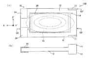
まず、本実施形態に係る圧電振動素子について、図面を参照しながら説明する。図1及び図2は、本発明の一実施形態に係る圧電振動素子100の構成を示す概略図である。図1(a)は、圧電振動素子100の平面図であり、図1(b)は、同図(a)のP1−P1断面図であり、図1(c)は、同図(a)のP2−P2断面図である。図2(a)は、図1(a)のQ1−Q1断面図であり、図2(b)は、図1(a)のQ2−Q2断面図、又はQ2’−Q2’断面図である。
本発明の圧電振動素子100は、中央に位置する多段メサ構造の励振部14、及び励振部14の周縁に連設形成された薄肉の周辺部12を有する圧電基板10と、励振部14の両主面上に夫々対向配置された励振電極20と、各励振電極20から圧電基板10の端部に向かって延びる引出電極22と、引出電極22の端部であり且つ圧電基板10の2つの角隅部に夫々形成されたパッド24と、を概略備えている。
励振部14は圧電基板の中央部を両主面方向へ突出させた厚肉部であり、周辺部12は励振部14の外周側面の少なくとも一部の厚み方向中間部から外径方向へ張出し形成されている。
1. Piezoelectric Vibration Element First, a piezoelectric vibration element according to this embodiment will be described with reference to the drawings. 1 and 2 are schematic views showing the configuration of a
The
The
圧電基板10は、その中央に位置し主たる振動領域となる励振部14と、励振部14より薄肉で励振部14の周縁に沿って形成された周辺部12と、を有している。平面形状がほぼ矩形である励振部14の対向する2つの側面(長手方向に沿った両側面)は夫々無段差状の1つの平面であり、励振部14の他の対向する2つの側面(短辺方向に沿った2つの側面)は夫々厚み方向に段差部を有した構造をしている。
各励振電極20に交番電圧を印加すると、圧電振動素子100は固有の振動周波数で励振される。励振された振動変位が十分に減衰する領域の周辺部12の表裏面には、圧電基板10の主面方向と直交する突起部11が少なくとも各一個形成されている。
突起部11は、図1、図2に示した例では、圧電基板10の2つの角隅部(図1(a)の左側)に夫々形成されたパッド24と対向する角隅部(図1(a)の右側)に表裏各2個形成されている。即ち、圧電基板10の周辺部12の角隅部に、周辺部12の表裏面に形成された突起部11が各2個設けられている。表裏の突起部11の厚さと周辺部12の厚さとの合計は、励振部14の中央の厚さと等しく構成することができる。
The
When an alternating voltage is applied to each
In the example shown in FIGS. 1 and 2, the
図3は、圧電振動素子100の平面図上に、圧電振動素子100が励振された際に生じる振動変位エネルギー(振動変位の二乗とその位置の質量との積)が等しい点を結んでできる等力線を一点鎖線で示している。図3に示す圧電振動素子100では、励振部14がX軸方向に長い矩形状をしているので、等力線はX軸方向の長径が大きく、Z’軸方向の短径が小さい楕円状となる。振動変位の大きさは励振部14の中心部で最大で、中心部から離間するにつれて小さくなる。即ち、励振電極20上ではX軸方向、Z’軸方向とも余弦上に分布し、励振電極20のない領域では指数関数的に減衰する。
図1に示す圧電振動素子100では、突起部11は振動変位エネルギーが十分に減衰した領域、即ち周辺部12の角隅部に設けている。このため、突起部11を設けても、圧電振動素子100の振動変位部に影響を及ぼすことはほぼない。つまり、圧電振動素子100の電気的特性は何ら変わる所はない。
FIG. 3 is formed on the plan view of the
In the
ところで、水晶等の圧電材料は三方晶系に属し、図4に示すように互いに直交する結晶軸X、Y、Zを有する。X軸、Y軸、Z軸は、夫々電気軸、機械軸、光学軸を呼称される。ATカット水晶基板101は、XZ面をX軸の回りに角度θだけ回転させた平面に沿って、水晶から切り出された平板である。ATカット水晶基板101の場合は、θは略35°15′である。なお、Y軸及びZ軸をX軸の周りにθ回転させ、夫々Y’軸、及びZ’軸とする。従って、ATカット水晶基板101は、直交する結晶軸X、Y’、Z’を有する。ATカット水晶基板101は、厚み方向がY’軸であって、Y’軸に直交するXZ’面(X軸及びZ’軸を含む面)が主面であり、厚みすべり振動が励振される。このATカット水晶基板101を加工して、圧電基板10を得ることができる。
即ち、圧電基板101は、図4に示すようにX軸(電気軸)、Y軸(機械軸)、Z軸(光学軸)からなる直交座標系のX軸を中心として、Z軸をY軸の−Y方向へ傾けた軸をZ’軸とし、Y軸をZ軸の+Z方向へ傾けた軸をY’軸とし、X軸とZ’軸に平行な面で構成され、Y’軸に平行な方向を厚みとするATカット水晶基板からなる。
By the way, piezoelectric materials such as quartz belong to the trigonal system and have crystal axes X, Y, and Z orthogonal to each other as shown in FIG. The X axis, the Y axis, and the Z axis are referred to as an electric axis, a mechanical axis, and an optical axis, respectively. The AT-cut
That is, as shown in FIG. 4, the
圧電基板10は、図1(a)に示すように、Y’軸に平行な方向(以下、「Y’軸方向」という)を厚み方向として、X軸に平行な方向(以下、「X軸方向」という)を長辺とし、Z’軸に平行な方向(以下、「Z’軸方向」という)を短辺とする矩形の形状を有することができる。圧電基板10は、励振部14と、励振部14の周縁に沿って形成された周辺部12と、を有する。ここで、「矩形の形状」とは、文字通り矩形状と、矩形の角部が面取りされた形も含むものとする。
周辺部12は、図1、図2に示すように、励振部14の周面(側面)の少なくとも一部に形成され、励振部14より小さい厚み(薄肉)を有する。
As shown in FIG. 1A, the
As shown in FIGS. 1 and 2, the
図1、図2に示すように本例に係る励振部14は、その全周を周辺部12に囲まれており、周辺部12のY’軸方向の厚みよりも大きい厚み(厚肉)を有する。即ち、励振部14は、図1(b)及び図2(a)に示すように、周辺部12に対してY’軸方向に突出している。図示の例では、励振部14は周辺部12に対して、+Y’軸側と−Y’軸側とに突出している。励振部14は、例えば対称の中心となる点(図示せず)を有し、この中心点に関して点対称となる形状を有することができる。
励振部14は、図1(a)に示すように、X軸方向を長辺とし、Z’軸方向を短辺とする矩形の形状を有する。即ち、励振部14はX軸に平行な辺を長辺とし、Z’軸に平行な辺を短辺としている。そのため、励振部14は、X軸方向に延びる側面14a、14bと、Z’軸方向に延びる側面14c、14dと、を有する。即ち、X軸方向に延びる側面14a、14bの長手方向は、X軸方向であり、Z’軸方向に延びる側面14c、14dの長手方向は、Z’軸方向である。図示の例では、側面14a、14bのうち、側面14aが+Z’軸側の側面であり、側面14bが−Z’軸側の側面である。また、側面14c、14dのうち、側面14cが−X軸側の側面であり、側面14dが+X軸側の側面である。
As shown in FIG. 1 and FIG. 2, the
As shown in FIG. 1A, the
X軸方向に延びる側面14aは、例えば図1(b)に示すように、周辺部12に対して、+Y’軸側と+Y’軸側とに夫々突出して形成されている。このことは側面14b、14c、14dについても同様である。X軸方向に延びる側面14a、14bの各々は、図1(b)に示すように1つの平面内にある無段差状となっている。即ち、+Y’軸側の側面14aは、1つの平面内であり、−Y’軸側の側面14aは、1つの平面内である。同様に、+Y’軸側の側面14bは、1つの平面内であり、−Y’軸側の側面14bは、1つの平面内である。
なお、本発明に係る記載において、「1つの平面内」とは、励振部14の側面が平坦な面である場合と、水晶の結晶の異方性の分だけ凹凸を有する場合と、を含む。即ち、フッ酸を含む溶液をエッチング液としてATカット水晶基板を加工すると、励振部14の側面は水晶結晶のR面が露出して、XY’面と平行な場合と、水晶結晶のm面が露出して、水晶の結晶異方性の分だけ凹凸を有する場合とがある。本発明に係る記載では、このような水晶結晶のm面による凹凸を有する側面についても「1つの平面内」にあるとしている。便宜上、図1(a)及び図2(a)では、m面による凹凸は省略している。なお、レーザーによってATカット水晶基板を加工することにより、水晶結晶のR面のみを露出することも可能である。
For example, as shown in FIG. 1B, the
In the description according to the present invention, “in one plane” includes the case where the side surface of the
Z’軸方向に延びる側面14c、14dの各々は、図2(a)に示すように、段差を有する。励振部14は、中央に位置する最大厚みを有した第1部分15と、第1部分15より小さい厚みを有する第2部分16と、を有し、側面14c、14dの段差は、第1部分15及び第2部分16の各厚みの差によって形成されている。図示の例では、側面14c、14dは、第1部分15のY’Z’平面に平行な面と、第2部分16のXZ’面に平行な面と、第2部分16のY’Z’平面に平行な面と、によって構成される。
Each of the side surfaces 14c and 14d extending in the Z′-axis direction has a step as shown in FIG. The
図1(a)及び図2(a)に示すように、例えば第2部分16は、第1部分15をX軸方向両側から挟むように形成されている。そのため、図1(b)に示すように、X軸方向に延びる側面14a、14bは、第1部分15の側面によって形成されている。このように励振部14は、厚みの異なる2種類の部分15、16を有しており、圧電振動素子100は、2段型(多段型)のメサ構造を有していると言える。
As shown in FIGS. 1A and 2A, for example, the
励振部14は、厚みすべり振動を主振動として振動することができる。励振部14が2段型のメサ構造であることによって、圧電振動素子100は、エネルギー閉じ込め効果を有することができる。
ここで、圧電基板10のZ’軸方向の寸法(短辺の寸法)をZとし、励振部14の短辺の寸法をMzとし、励振部の厚み(励振部14の第1部分15の厚み)をtとすると、下記式(1)の関係を満たすことが好ましい。
8≦Z/t≦11、且つ0.6≦Mz/Z≦0.8 (1)
これにより、厚みすべり振動と輪郭振動等の不要モードとの結合を抑圧することができ、CI値の低減と周波数温度特性の改善を図ることができる。(詳細は後述)。このような厚みすべり振動と輪郭振動との結合は、一般的に圧電基板の面積が小さいほど抑圧するのが難しい。そのため、例えば圧電基板10のX軸方向の寸法(長辺の寸法)をXとした場合に、下記式(2)の関係を満たすような小型の圧電振動素子100において、上記式(1)の関係を満たすように設計すると、より顕著に厚みすべり振動と輪郭振動との結合を抑圧することができる。
X/t≦17 (2)
The
Here, the dimension (short side dimension) in the Z′-axis direction of the
8 ≦ Z / t ≦ 11 and 0.6 ≦ Mz / Z ≦ 0.8 (1)
Thereby, the coupling between the thickness shear vibration and the unnecessary mode such as the contour vibration can be suppressed, and the CI value can be reduced and the frequency temperature characteristic can be improved. (Details will be described later). Such coupling between the thickness shear vibration and the contour vibration is generally difficult to suppress as the area of the piezoelectric substrate is smaller. Therefore, for example, in a small
X / t ≦ 17 (2)
励振電極20は励振部14に形成されている。図1(b)及び図2(a)に示す例では、励振電極20は励振部14を表裏に挟んで形成されている。より具体的には、励振電極20は、圧電基板10の両主面(XZ’面に平行な面)の振動領域(励振部14)に、表裏で対向するように配置されている。励振電極20は励振部14に電圧を印加することができる。励振電極20は、例えば引出電極22を介してパッド24と接続している。パッド24は、例えば圧電振動素子100を駆動するためのICチップ(図示せず)と電気的に接続されている。励振電極20、引出電極22、及びパッド24の材質としては、例えば、圧電基板10側からクロム、金をこの順で積層したものを用いることができる。
The
本実施形態に係る圧電振動素子100は、例えば以下の特徴を有する。
厚みすべり振動と、無段差状の平面と直交する方向の輪郭振動等の不要モードとの結合を抑制でき、CI値を低減することができるという効果がある。(詳細は後述)また、圧電基板上の振動変位が十分に減衰する領域の両主面上に突起部11を設けることにより、パッケージに実装する際に、励振部に形成した励振電極とパッケージの内側の面が接触する虞がなくなると言う効果がある
また、図1に示す実施形態例のように、水晶を用いて圧電振動素子を構成すると、圧電振動素子の周波数温度特性が優れていると共に、厚みすべり振動と、Z’軸方向の輪郭振動との結合を抑制でき、CI値を低減することができるという効果がある。また、圧電基板上であって振動変位が十分に減衰する領域の両主面上に突起部を設けることにより、パッケージに実装する際に、励振部に形成した励振電極とパッケージの内側の面が接触する虞がなくなるという効果がある。
The
Coupling between thickness shear vibration and unnecessary modes such as contour vibration in a direction orthogonal to the stepless plane can be suppressed, and the CI value can be reduced. (Details will be described later) Further, by providing the
図1に示す実施形態例のように、圧電基板10のパッド24と対向する周辺部12の角隅部に突起部11が設けられているので、圧電基板10上に励起される主振動の厚みすべり振動の振動変位が十分に減衰しており、その動作を阻害することなく、電気的特性には変化はない。しかも、突起部11を有する圧電振動素子100をパッケージに実装する際に、励振部に形成した励振電極とパッケージの内側の面とが接触する虞が除かれるので、圧電振動子を製作する際に、歩留まりが大幅に改善されるという効果がある。
また、圧電振動素子100によれば、上述のとおり、圧電基板10の短辺の寸法Z、励振部14の短辺の寸法Mz、及び励振部14の厚みtを式(1)の関係を満たすようにすることにより、CI値の低減を図ることができる。
圧電振動素子100によれば、上述のとおり、X辺比(X/t)を式(2)の関係を満たすようにすることにより、小型化を図りつつCI値の低減を図ることができる。
As in the embodiment shown in FIG. 1, since the
Further, according to the
According to the
2.圧電振動素子の製造方法
次に、本実施形態に係る圧電振動素子の製造方法について、図面を参照しながら説明する。図5乃至図11は、本実施形態に係る圧電振動素子100の製造工程を模式的に示す図である。なお、図5乃至図11において、(a)は平面図であり、(b)は(a)のP3−P3断面図であり、(c)は(a)のQ3−Q3断面図である。また、図9乃至図11において、(d)はQ4−Q4、又はQ4’−Q4’断面図である。
2. Next, a method for manufacturing a piezoelectric vibration element according to this embodiment will be described with reference to the drawings. 5 to 11 are diagrams schematically showing a manufacturing process of the piezoelectric vibrating
図5に示すように、ATカット水晶基板101の表裏主面(XZ’平面に平行な面)に耐蝕膜30を形成する。耐蝕膜30は、例えば、スパッタ法や真空蒸着法などによりクロム及び金をこの順で積層した後、このクロム及び金をパターニングすることによって形成される。パターニングは、例えば、フォトリソグラフィ技術及びエッチング技術によって行われる。耐蝕膜30は、ATカット水晶基板101を加工する際に、エッチング液となるフッ酸を含む溶液に対して耐蝕性を有する。
図6に示すように、耐蝕膜30上にポジ型のフォトレジスト膜を塗布した後、このフォトレジスト膜を露光及び現像して、所定の形状を有するレジスト膜40を形成する。レジスト膜40は、耐蝕膜30の一部を覆うように形成される。
As shown in FIG. 5, a corrosion-
As shown in FIG. 6, after applying a positive photoresist film on the corrosion-
次いで、図7に示すように、マスクMを用いて再度レジスト膜40の一部を露光して、感光部42を形成する。マスクMは、図7(a)に示すようにY’軸方向から見てレジスト膜40に対して交差するように配置する。即ち、マスクMのX軸方向の寸法はレジスト膜40のX軸方向の寸法より小さく、マスクMのZ’軸方向の寸法はレジスト膜40のZ’軸方向の寸法より大きい。このようなマスクMを用いて露光することにより、図7(c)に示すようにZ’軸方向から見てレジスト膜40の両側に感光部42を形成することができる。
次いで、図8に示すように、耐蝕膜30をマスクとしてATカット水晶基板101をエッチングする。エッチングは、例えば、フッ化水素酸(フッ酸)とフッ化アンモニウムとの混合液をエッチング液として行われる。これにより、図8(a)に示すように圧電基板10の外形(Y’軸方向から見たときの形状)が形成される。
Next, as shown in FIG. 7, a part of the resist
Next, as shown in FIG. 8, the AT cut
次いで、図9に示すように、レジスト膜40をマスクとして、所定のエッチング液で耐蝕膜30をエッチングした後、さらに、上述の混合液をエッチング液としてATカット水晶基板101を所定の深さまでハーフエッチングする。これにより、励振部14の外形と突起部11の外形とが形成される。
次いで、図10に示すように、レジスト膜40の感光部42を現像して除去する。これにより、耐蝕膜30の一部が露出する。なお、感光部42を現像する前に、例えば、真空又は減圧雰囲気下で放電によりつくられた酸素プラズマによって、レジスト膜40の表面に形成された変質層(図示せず)をアッシングする。これにより、確実に感光部42を現像して除去することができる。
次いで、図11に示すように、レジスト膜40をマスクとして、所定のエッチング液で耐蝕膜30の露出部分をエッチング除去した後、さらに、上述の混合液をエッチング液としてATカット水晶基板101を所定の深さまでハーフエッチングする。これにより、X軸方向に延びる側面14a、14bの各々を1つの平面内に形成することができる。また、Z’軸方向に延びる側面14c、14dの各々に段差を形成することができる。また、圧電基板10の周辺部12の表裏の角隅部に、周辺部12と直交する突起部11を夫々形成することができる。
Next, as shown in FIG. 9, after etching the corrosion-
Next, as shown in FIG. 10, the
Next, as shown in FIG. 11, using the resist
以上の工程により、周辺部12、励振部14、及び突起部11を有する圧電基板10を形成することができる。
図1、図2に示すように、レジスト膜40及び耐蝕膜30を除去した後、圧電基板10に励振電極20、引出電極22、及びパッド24を形成する。励振電極20、引出電極、及びパッド24は、例えばスパッタ法や真空蒸着法などにより、クロム及び金をこの順で積層した後、このクロム及び金をパターニングすることによって形成される。
Through the above steps, the
As shown in FIGS. 1 and 2, after removing the resist
以上の工程により、本実施形態に係る圧電振動素子100を製造することができる。
圧電振動素子100の製造方法によれば、励振部14の外形を形成するために用いたレジスト膜40を現像して感光部を除去した後、再度レジスト膜40を用いてX軸方向に延びる側面14a、14bを露出することができる。ここで、感光部42を形成するためのマスクMは、X軸方向の寸法がレジスト膜40の寸法より小さく、Z’軸方向の寸法がレジスト膜40の寸法より大きい。そのため、精度よく側面14a、14bの各々を1つの平面内に形成することができる。例えば、励振部14を形成するために、2回のレジスト膜を塗布する場合(例えば、第1レジスト膜を用いて励振部の外形を形成した後、第1のレジスト膜を剥離し、新たに第2レジスト膜を塗布して励振部の側面を露出する場合)は、第1のレジスト膜と第2のレジスト膜との間で合わせずれが生じ、励振部の側面を1つの平面内に形成できないことがある。圧電振動素子100の製造方法では、このような問題を解決することができる。
また、圧電振動素子100の製造方法によれば、圧電基板10の角隅部の2つのパッド24と対向する周辺部12の角隅部に、夫々周縁部12の表裏に直交する突起部11を形成することができる。
Through the above steps, the
According to the method for manufacturing the
In addition, according to the method for manufacturing the
3.圧電振動素子の変形例
次に、本実施形態の変形例に係る圧電振動素子について、図面を参照しながら説明する。図12(a)は、本実施形態の変形例に係る圧電振動素子200を模式的に示す平面図である。図12(b)は、(a)のP6−P6断面図であり、図12(c)は、(a)のP7−P7断面図である。図13(a)は、図12(a)のQ6−Q6断面図であり、図13(b)は、図12(a)のQ7−Q7断面図、又はQ7’−Q7’断面図である。以下、本実施形態の変形例に係る圧電振動素子200において、本実施形態に係る100の構成部材と同様な構造、機能を有する部材については同一符号を付し、その詳細な説明を省略する。
3. Next, a piezoelectric vibration element according to a modification of the present embodiment will be described with reference to the drawings. FIG. 12A is a plan view schematically showing a
圧電振動素子100の例では、図1、図2に示すように、厚みの異なる第1部分15、及び第2部分16を有する2段型のメサ構造について説明した。
これに対して、圧電振動素子200では、図12、図13に示すように、3段のメサ構造を有する。即ち、圧電振動素子200の励振部14は、第1部分15、第2部分16に加え、第2部分16より厚みの小さい第3部分17を有する。図12、図13に示す例では、第3部分17は、第1部分15、及び第2部分16をX軸方向から挟むように形成されている。
Z’軸方向に延びる側面14c、14dの段差は、図13(a)に示すように、第1部分15、第2部分16、及び第3部分17の厚みの差によって形成されている。図示の例では、側面14c、14dは、第1部分15のY’Z’平面に平行な面と、第2部分16のXZ’平面に平行な面と、第2部分16のY’Z’平面に平行な面と、第3部分17のXZ’平面に平行な面と、第3部分17のY’Z’平面に平行な面と、によって構成されている。また、第1部分15、第2部分16、及び第3部分17から成る励振部14は、第3部分17の周縁に沿って、第3部分17の厚みより薄い周辺部12が形成されている。励振部14に表裏対向して形成された励振電極20、各励振電極20からの引出電極22、及び各引出電極22の終端である2つのパッド24も、圧電振動素子100と同様に形成されている。圧電基板10の角隅部に設けた2つのパッド24に対向して、周辺部12の角隅部に周辺部12に直交して表裏に夫々突起部11が形成されている。
In the example of the
On the other hand, the
The steps of the side surfaces 14c and 14d extending in the Z′-axis direction are formed by the thickness differences of the
圧電振動素子200は、圧電振動素子100の製造方法を適用して製造することができる。即ち、図10に示すように感光部42を現像して除去した後、再度レジスト膜40を露光して所定形状の第2感光部(図示せず)を形成する。次に、第2感光部を有するレジスト膜40をマスクとして、耐蝕膜30及びATカット水晶基板101をエッチングする。次にアッシングを行ってレジスト膜40の変質層を除去した後、第2感光部を現像して除去する。次に、第2感光部が除去されたレジスト膜40をマスクとして、耐蝕膜30及びATカット水晶基板101をエッチングする。以上の工程により、3段型のメサ構造と、圧電基板10の周辺部12の角隅部の表裏に、周辺部12と直交する突起部11を夫々形成することができる。圧電基板10に3段型のメサ構造の励振部に対向する励振電極20と、各励振電極20からの引出電極22、及び引出電極22の終端である2個のパッド24を形成することにより、圧電振動素子200を製造することができる。
The
圧電振動素子200によれば、2段型のメサ構造を有する圧電振動素子100に比べて、エネルギー閉じ込め効果をより高めることができる。また、圧電振動素子200によれば、圧電基板10の角隅部の2つのパッド24と対向する周辺部12の角隅部に、夫々周縁部12の表裏に直交する突起部11を形成したので、パッケージに実装する際に歩留まりを大幅に改善することができる。
なお、上述の例では、3段型のメサ構造を有する圧電振動素子200について説明したが、本願に係る発明は多段型のメサ構造において、励振部のX軸方向に延びる側面の各々が1つの平面内にあれば、メサ構造の段数(段差の数)は特に限定されない。
According to the
In the above-described example, the
図14(a)は、圧電振動素子の他の変形例110(圧電振動素子100をベースに示しているが圧電振動素子200をベースにしてもよい)の平面図であり、同図(b)は、(a)のQ2−Q2断面図、又はQ2’−Q2’断面図である。圧電振動素子110は、中央部にメサ構造の励振部14が形成され、励振部14の周縁には薄肉の周辺部12が形成された圧電基板10と、励振部14の表裏に対向して形成された励振電極20と、各励振電極20から圧電基板10の端部に向かって延びる引出電極22と、引出電極22の終端であるパッド24と、を備えている。また、圧電基板10の角隅部に設けた2つのパッド24と対向する周辺部12上で、Z’軸(短辺)に沿った端縁に沿って設けられた第1の突起部分11aと、第1の突起部分11aの長手方向両端部から夫々X軸に沿った方向へ屈曲して連設された第2の突起部分11bと、を備えたコ字状の突起部11が表裏に形成されている。周辺部12の厚みと表裏の突起部11の厚みとを加算した厚さは、励振部14の中央の厚さと等しくすることができる。
FIG. 14A is a plan view of another modified example 110 of the piezoelectric vibration element (shown based on the
図15(a)は、圧電振動素子の他の変形例120の平面図であり、同図(b)は、(a)のQ1−Q1断面図である。圧電基板10の励振部14、励振電極20、引出電極22、パッド24は、図1、図2示した圧電振動素子100と同様であるので、説明を省略する。圧電基板10の角隅部に設けた2つのパッド24と対向する周辺部12上の表裏に、Z’軸(短辺)に沿った端縁に沿って細帯状の突起部11が夫々形成されている。
FIG. 15A is a plan view of another
図16(a)は、圧電振動素子の他の変形例130の平面図であり、同図(b)は、(a)のQ2−Q2断面図、又はQ2’−Q2’断面図である。圧電基板10の励振部14、励振電極20、引出電極22、パッド24は、図1、図2示した圧電振動素子100と同様であるので、説明を省略する。圧電基板10の角隅部に設けた2つのパッド24と対向する周辺部12の角隅部に、且つ周辺部12に直交した表裏に、圧電基板10の長辺(X軸方向)に沿って短尺な細帯状の突起部11が夫々形成されている。
FIG. 16A is a plan view of another
図14の実施形態例に示すように、圧電基板10の端部にコ字状の突起部11(11a、11b)を形成すると、圧電振動素子がパッケージにX軸方向に回転して接着固定されても、励振電極がパッケージの内側の面に接触する虞がなく、圧電振動子を製作する際に、歩留まりが大幅に改善されるという効果がある。
図15の実施形態例に示すように、圧電基板上のZ’軸に沿った端縁に沿ってその全長に渡って突起部11を形成すると、エッチング等により突起部に多少の変形が生じてもその機能、即ちパッケージに実装する際に、励振電極とパッケージの内側の面とが接触する虞を除くという機能を損なうことはないので、圧電振動子を製作する際に、歩留まりが大幅に改善されるという効果がある。
また、図1、図2、図12、図13、図14乃至図16の実施形態例に示すように、励振部14の厚さと、表裏の突起部11の各厚みと周辺部12の厚みを合計した厚みと、を等しくすることにより圧電基板の製造が容易であると共に、励振電極がパッケージの内側の面に接触する虞がなく、圧電振動子を製作する際に、歩留まりが大幅に改善されるという効果がある。
As shown in the embodiment of FIG. 14, when the U-shaped protrusion 11 (11a, 11b) is formed at the end of the
As shown in the embodiment of FIG. 15, when the
In addition, as shown in the embodiment examples of FIGS. 1, 2, 12, 13, and 14 to 16, the thickness of the
4.圧電振動子
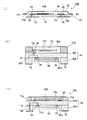
次に、本実施形態に係る圧電振動子について、図面を参照しながら説明する。図17は、本実施形態に係る圧電振動子300を模式的に示す断面図である。
図17(a)は、圧電振動子300の構成を示す長手方向(X軸方向)の断面図であり、図2(a)に示した圧電振動素子100の断面図と同様な位置における断面図である。図17(b)は、圧電振動子300の短手方向(Z’軸方向)の端部における長手方向(X軸方向)の断面図である。圧電振動子300は、図17(a)に示すように、本発明に係る圧電振動素子(図示の例では圧電振動素子100)と、パッケージ50と、を含む。
パッケージ50は、キャビティー52内に圧電振動素子100を収容することができる。パッケージ50の材質としては、例えば、セラミック、ガラス等が挙げられる。キャビティー52は、圧電振動素子100が動作するための空間となる。キャビティー52は密閉され、減圧空間や不活性ガス雰囲気とされる。
圧電振動素子100は、パッケージ50のキャビティー52内に収容されている。図示の例では、圧電振動素子100は、導電性接着剤60を介して、片持ち梁状にキャビティー52内に固定されている。導電性接着剤60としては、例えば、半田、銀ペーストを用いることができる。
4). Next, the piezoelectric vibrator according to the present embodiment will be described with reference to the drawings. FIG. 17 is a cross-sectional view schematically showing the
17A is a cross-sectional view in the longitudinal direction (X-axis direction) showing the configuration of the
The
The
図17(a)、(b)に示した図では、圧電振動素子100の両主面がパッケージ50の内底面図(又は蓋部材)と並行するように構成された例を示したが、導電性接着剤60の塗布量や粘度によっては、図17(c)に示す断面図のように、パッケージ50の内底面の方へ傾くか、逆に蓋部材の方へ反る場合がある。しかし、本発明の圧電振動素子(図示の例は圧電振動素子100)の場合は、圧電基板10の角隅部に設けたパッド24と対向する周辺部12の角隅部の表裏に突起部11を形成してあるので、圧電振動素子100がパッケージ50の内底面側に傾いた場合でも、逆に蓋部材側に反った場合でも、励振部14に形成した励振電極20が内底面、蓋部材の何れにも接触することがない。これは、図17(d)に示すように、一様な厚みの基板62の一方の側(図では左側)を基台65に接着剤60で固定した場合に、基板62が下方へ傾いても基板62の他方の側(図では右側)の下部先端Aが基台65の上面に接するが、基板62の他の部分は、基台65の上面に接しないことからも容易に理解される。
なお、図示はしないが、パッケージ50には、圧電振動素子100を発振させるためのICチップが収容されていてもよい。ICチップは、導電性接着剤60を介して、パッド24と電気的に接続されている。
図17の実施形態に示すように、圧電振動子300によれば、本発明に係る圧電振動素子100を有するので、CI値の低減を図ることができる。また、圧電振動子300によれば、圧電振動素子100のパッド24と対向する角隅部、又は対向する端縁に沿って突起部11を設けたので、圧電振動素子10をパッケージ50に収容する際に、励振電極20がパッケージ底面、又は蓋部材に接触することがないので、圧電振動子300の歩留まりが大幅に改善されるという効果がある。
17A and 17B illustrate an example in which both main surfaces of the
Although not shown, the
As shown in the embodiment of FIG. 17, according to the
5.実験例
以下に実験例を示し、本発明をより具体的に説明する。なお、本発明は、以下の実験例によってなんら限定されるものではない。
<5.1 圧電振動素子の構成>
実施例1として、図1、図2に示す2段型のメサ構造を有する圧電振動素子100を用いた。実施例1では、フッ酸を含む溶液によるウエットエッチングによりATカット水晶基板を加工し、周辺部12及び励振部14を有する圧電基板10を形成した。圧電基板10は、対称の中心となる点(図示せず)に関して点対称に形成した。励振部14(第1部分15)の厚みtを0.065mmとし、振動周波数を24MHzに設定した。また、圧電基板10の長辺の寸法Xを1.1mm(即ち、X辺比X/tを17)とし、圧電基板10の短辺の寸法Zを0.629mm(即ち、Z辺比Z/tを9.7)とし、励振部14の短辺寸法Mzを0.43mmとし、X軸方向に延びる側面14a、14bの各々を1つの平面内に形成した。
5. Experimental Example An experimental example is shown below to describe the present invention more specifically. The present invention is not limited by the following experimental examples.
<5.1 Configuration of Piezoelectric Vibration Element>
As Example 1, a
比較例としては、図18に示す圧電振動素子1000を用いた。図18(a)は平面図であり、図18(b)は、(a)のQ8−Q8断面図である。
比較例1では、励振部1014を図18(b)に示すように、X軸方向に延びる側面の各々が段差を有すること以外は、実施例1の励振部14と同様な形状に形成した。なお、図18に示した、周辺部1012、励振電極1020、引出電極1022、及びパッド1024は、夫々図1、図2に示した、周辺部12、励振電極20、引出電極22、及びパッド24に対応している。
As a comparative example, a
In Comparative Example 1, the
<5.2 CI値の分布測定結果>
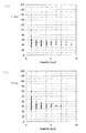
上述の実施例1及び比較例1を、夫々200個ずつ製作し、これらをパッケージに収容してCI値(室温)を測定した。図19は測定個数に対するCI値を示したグラフであり、図19(a)は実施例1の測定結果であり、図19(b)は比較例1の測定結果である。即ち、図19は、実施例1及び比較例1におけるCI値の分布を示している。
図19より、実施例1では全ての試料においてCI値は80Ω以下であり、比較例1よりCI値が低いことが分かった。さらに、実施例1では、比較例1に比べてCI値のばらつきが小さいことが分かった。即ち、励振部のX軸方向に延びる側面の各々を1つの平面内に形成することにより、CI値の低減を図ることができた。これは、X軸方向に延びる側面の各々を1つの平面内に形成することで、Z’軸方向における厚みすべり振動と輪郭振動等の不要モードとの結合を抑制できたためであると推察される。
<5.2 CI measurement result of distribution>
200 pieces of each of the above-described Example 1 and Comparative Example 1 were manufactured, and these were housed in a package, and the CI value (room temperature) was measured. FIG. 19 is a graph showing the CI value with respect to the measured number, FIG. 19A shows the measurement result of Example 1, and FIG. 19B shows the measurement result of Comparative Example 1. That is, FIG. 19 shows the CI value distribution in Example 1 and Comparative Example 1.
From FIG. 19, it was found that in all samples in Example 1, the CI value was 80Ω or less, which was lower than that in Comparative Example 1. Furthermore, in Example 1, it turned out that the dispersion | variation in CI value is small compared with the comparative example 1. FIG. That is, the CI value can be reduced by forming each of the side surfaces of the excitation unit extending in the X-axis direction in one plane. This is presumably because the formation of each side surface extending in the X-axis direction in one plane can suppress the coupling between the thickness shear vibration in the Z′-axis direction and unnecessary modes such as contour vibration. .
<5.3 Mz/Zに対するCI値評価>
実施例1の圧電振動素子において、励振部14の厚みtを0.065mm、及び励振部14の短辺Mzの寸法を0.43mmに固定し、圧電基板10の短辺の寸法Zを0.46mm、0.5mm、0.54mm、0.59mm、0.65mm、0.72mm、0.81mm、0.92mmと振って、CI値(室温)を測定した。測定は、圧電振動素子をパッケージに収容して行った。図20は、Mz/ZとCI値との関係を示したグラフである。
図20より、Mz/Zが0.6以上0.8以下の範囲では、CI値は60Ω程度と低いことが分かった。このときのZは0.54mm以上0.72mm以下であり、Z辺比(Z/t)は8以上11以下となる。以上より、Z辺比(Z/t)の範囲を8≦Z/t≦11とし、とし、且つMz/Zの範囲を0.6≦Mz/Z≦0.8とすることにより(即ち、上記式(1)を満たすことにより)、CI値の低減を図れることが分かった。これは、式(1)を満たすようにZ/t及びMz/Zを設計することにより、一層Z’軸方向における厚みすべり振動と輪郭振動等の不要モードとの結合を抑制できたためであると推察される。
なお、Mzを0.4mmとし、Zを0.65mmとした(即ち、Mz/Z=0.6)圧電振動素子、及びMzを0.48mmとし、Zを0.6mmとした(即ち、Mz/Z=0.8)圧電振動素子についてもCI値を測定したところ、共に60Ω程度であった。このことから、Mz=0.43mmの場合に限定されることなく、上記式(1)を満たす限り、CI値の低減を図ることができるといえる。
<CI value evaluation for 5.3 Mz / Z>
In the piezoelectric vibration element of Example 1, the thickness t of the
From FIG. 20, it was found that the CI value is as low as about 60Ω in the range where Mz / Z is 0.6 or more and 0.8 or less. At this time, Z is 0.54 mm or more and 0.72 mm or less, and the Z side ratio (Z / t) is 8 or more and 11 or less. From the above, by setting the range of the Z side ratio (Z / t) to 8 ≦ Z / t ≦ 11 and the range of Mz / Z to 0.6 ≦ Mz / Z ≦ 0.8 (that is, It was found that the CI value can be reduced by satisfying the above formula (1). This is because by designing Z / t and Mz / Z so as to satisfy Equation (1), the coupling between the thickness shear vibration in the Z′-axis direction and unnecessary modes such as contour vibration can be further suppressed. Inferred.
In addition, Mz was set to 0.4 mm and Z was set to 0.65 mm (that is, Mz / Z = 0.6), and Mz was set to 0.48 mm and Z was set to 0.6 mm (that is, Mz /Z=0.8) The CI value of the piezoelectric vibrating element was measured and found to be about 60Ω. From this, it can be said that the CI value can be reduced as long as the above formula (1) is satisfied without being limited to the case of Mz = 0.43 mm.
以上の実験例は、図1、図2に示した2段型のメサ構造を有する圧電振動素子について行ったが、本実験結果は、例えば図12、図13に示したような多段メサ型のメサ構造を有する圧電振動素子にも適用することができる。 Although the above experimental example was performed on the piezoelectric vibration element having the two-stage type mesa structure shown in FIGS. 1 and 2, the result of this experiment is, for example, a multistage mesa type as shown in FIGS. 12 and 13. The present invention can also be applied to a piezoelectric vibration element having a mesa structure.
図21(a)は、本発明の電子デバイス400に係る実施形態の一例の断面図である。電子デバイス400は、本発明の圧電振動素子100(図21(a)では圧電振動素子100を示したが、本発明の他の圧電振動素子であってもよい)と、感温素子であるサーミスタ58と、圧電振動素子100及びサーミスタ58を収容するパッケージ50と、を概略備えている。パッケージ50は、パッケージ本体50aと、蓋部材50cとを備えている。パッケージ本体50aは、上面側に圧電振動素子100を収容するキャビティー52が形成され、下面側にサーミスタ58を収容する凹部54aが形成されている。キャビティー52の内底面の端部に複数の素子搭載用パッド55aが設けられ、各素子搭載用パッド55aは内部導体57で複数の実装端子53と導通接続されている。素子搭載用パッド55aに圧電振動素子100を載置し、各パッド24と各素子搭載用パッド55aとを、導電性接着剤60を介して電気的に接続し、固定する。パッケージ本体50aの上部には、コバール等からなるシールリングリング50bが焼成されており、このシールリングリング50bに蓋部材50cを載置し、抵抗溶接機を用いて溶接し、キャビティー52を気密封止する。キャビティー52内は真空にしてもよいし、不活性ガスを封入してもよい。
一方、パッケージ本体50aの下面側中央には凹部54aが形成され、凹部54aの上面には電子部品搭載用パッド55bが焼成されている。サーミスタ58は、電子部品搭載用パッド55bに半田等を用いて搭載される。電子部品搭載用パッド55bは、内部導体57で複数の実装端子53と導通接続されている。
FIG. 21A is a cross-sectional view of an example of an embodiment according to the
On the other hand, a
図21(b)は、同図(a)の変形例の電子デバイス410であって、電子デバイス400と異なる点は、パッケージ本体50aのキャビティー52底面に凹部54bが形成され、この凹部54bの底面に焼成された電子部品搭載パッド55bに、金属バンプ等を介してサーミスタ58が接続されている所である。電子部品搭載パッド55bは実装端子53と導通されている。つまり、圧電振動素子100と感温素子のサーミスタ58とが、キャビティー52内に収容され、気密封止されている。
以上では、圧電振動素子100とサーミスタ58とをパッケージ50に収容した例を説明したが、パッケージ50収容する電子部品としては、サーミスタ、コンデンサ、リアクタンス素子、半導体素子のうち少なくとも一つを収容した電子デバイスを構成することが望ましい。
FIG. 21 (b) shows an
In the above, the example in which the
図21(a)、(b)に示す実施形態例は、圧電振動素子100とサーミスタ58とをパッケージ50に収容した例である。このように構成すると、感温素子のサーミスタ58が圧電振動素子100の極めて近くに位置しているので、圧電振動素子100の温度変化を素早く感知することができるという効果がある。また、本発明の圧電振動素子と上記の電子部品とで電子デバイスを構成することにより、CIの小さな圧電振動素子を有する電子デバイスが構成できるので、多方面の用途に利用できるという効果がある。
The embodiment shown in FIGS. 21A and 21B is an example in which the
次に、本発明に係る圧電振動素子を使用した圧電振動子のパッケージに対して、圧電振動子を駆動し、増幅する発振回路を搭載したIC部品を組み付けることにより、圧電発振器を構築することができる。
図22(a)は、本発明の圧電発振器500に係る実施形態の一例の断面図である。圧電発振器500は、本発明の圧電振動素子100(図22(a)では圧電振動素子100を示したが、本発明の他の圧電振動素子であってもよい)と、単層の絶縁基板70と、圧電振動素子100を駆動するIC(半導体素子)88と、圧電振動素子100及びIC88を含む絶縁基板70の表面空間を気密封止する凸状の蓋部材80と、を概略備えている。絶縁基板70は、表面に圧電振動素子100及びIC88を搭載するための複数の素子搭載パッド74a、電子部品搭載パッド74bを有すると共に、裏面に外部回路との接続用の実装端子76を備えている。素子搭載パッド74a及び電子部品搭載パッド74bと実装端子76とは、絶縁基板70を貫通する導体78により、導通されている。更に、絶縁基板70表面に形成された導体配線(図示せず)により、素子搭載パッド74aと電子部品搭載パッド74bとは導通が図られている。金属バンプ等を用いてIC88を電子部品搭載パッド74bに搭載した後、素子搭載パッド74aに導電性接着剤60を塗布し、その上に圧電振動素子100のパッド24を載置し、恒温槽内で硬化させて導通・固定を図る。凸状の蓋部材80と絶縁基板70とは、絶縁基板70の上面周縁に塗布した低融点ガラス85によって密封される。このとき、封止工程を真空中で行うことにより内部を真空にすることができる。
Next, a piezoelectric oscillator can be constructed by assembling an IC component equipped with an oscillation circuit for driving and amplifying the piezoelectric vibrator to the package of the piezoelectric vibrator using the piezoelectric vibrator according to the present invention. it can.
FIG. 22A is a cross-sectional view of an example of an embodiment according to the
図22(b)は、本発明の他の実施形態の圧電発振器510の断面図である。圧電発振器510は、本発明の圧電振動素子100と、パッケージ本体90と、圧電振動素子100を駆動するIC88と、圧電振動素子100を気密封止する蓋部材90cと、を概略備えている。パッケージ本体90は、圧電振動素子100を収容するキャビティー52を有する上部90aと、IC88を収容する凹部90dを有する下部90bとから成る、所謂H型構造のパッケージ本体である。圧電振動素子100は、キャビティー52底部の端部に形成された素子搭載パッド74aに、導電性接着剤60を塗布し、この上に載置し、熱硬化することにより導通・固定される。IC88は、パッケージ本体90の下面側の凹部90dの上面に形成された電子部品搭載パッド74bに、金属バンプ79により接続・固定される。素子搭載パッド74a及び電子部品搭載パッド74bは、内部導体78により導通接続されている。パッケージ本体90の上部に焼成されたシールリング(図示せず)に蓋部材90cを載置し、抵抗溶接機等を用いて溶接し、気密封止する。キャビティー52内は真空にしてもよいし、不活性ガスを封入してもよい。
FIG. 22B is a cross-sectional view of a
図22(c)は、本発明の他の実施形態の圧電発振器520の断面図である。圧電発振器520は、本発明の圧電振動子300と、パッケージ本体90と、圧電振動子300を駆動するIC88と、圧電振動子300気密封止する蓋部材90cと、を概略備えている。パッケージ本体90は、圧電振動子300を収容するキャビティー52を有する上部90aと、ICを収容する凹部90dを有する下部90bとから成る、所謂H型構造のパッケージ本体である。圧電振動子300は、キャビティー52底部の両端部に形成された素子搭載パッド74aに載置され、半田又は金属バンプ等により接続固定される。IC88は、パッケージ本体90の下面側の凹部90dの上面に形成された素子搭載パッド74bに、金属バンプ79により接続・固定される。素子搭載パッド74a及び電子部品搭載パッド74bは、内部導体78により導通されている。パッケージ本体90の上部に焼成されたシールリング(図示せず)に蓋部材90cを載置し、抵抗溶接機を用いて溶接する。圧電振動素子は二重に気密封止されている。
IC88は、圧電振動子300を駆動する発振回路と、圧電振動子300の周囲の温度を感知する感温素子と、圧電振動子300の周波数温度特性を補償する補償回路と、電圧可変容量素子等を含むことができる。
FIG. 22C is a cross-sectional view of a
The
図22(a)の実施形態の圧電発振器500は、パッケージ内に本発明に係るCI値が小さな圧電振動素子100と、IC(発振回路を含む)88とを備えており、圧電発振器が小型化されると共に、発振回路の発振電流を小さくできるので、低消費電力化が図れるという効果がある。
図22(b)の実施形態の圧電発振器510は、パッケージ内に本発明に係るCI値が小さな圧電振動素子100と、IC(発振回路を含む)88とを備えており、圧電発振器低消費電力化が図れるという効果がある。更に、IC88を外部より調整可能することができるため、より周波数温度特性が優れ、多機能の圧電発振器を構成できるという効果がある。
図22(c)の実施形態の圧電発振器520は、パッケージに収容した圧電振動子300を用いているので、エージング等の周波数安定度が優れ、多機能で信頼性のある圧電発振器を構成できるという効果がある。
A
The
Since the
本発明は、前述した実施形態に限定されるものではなく、種々の変形が可能である。例えば、本発明は、実施形態で説明した構成と実質的に同一の構成(例えば、機能、方法及び結果が同一構成、あるいは目的及び効果が同一の構成)を含む。また、本発明は、実施形態で説明した構成の本質的でない部分を置き換えた構成を含む。また、本発明は、実施形態で説明した構成と同一の効果を奏する構成又は同一の目的を達成することができる構成を含む。また、本発明は、実施形態で説明した構成に公知技術を付加した構成を含む。
なお、上述した圧電発振器等の電子デバイスにおいては、圧電振動子に半導体素子(IC)に代表される電子部品を備えた構成として説明したが、少なくとも一以上の電子部品を備えることが好適である。そして前記電子部品としては、サーミスタ、コンデンサ、リアクタンス素子等を適用することができ、圧電振動片を発振源として用いた電子デバイスを構築することができる。
The present invention is not limited to the embodiments described above, and various modifications are possible. For example, the present invention includes configurations that are substantially the same as the configurations described in the embodiments (for example, configurations that have the same functions, methods, and results, or configurations that have the same purposes and effects). In addition, the invention includes a configuration in which a non-essential part of the configuration described in the embodiment is replaced. In addition, the present invention includes a configuration that achieves the same effect as the configuration described in the embodiment or a configuration that can achieve the same object. In addition, the invention includes a configuration in which a known technique is added to the configuration described in the embodiment.
In the electronic device such as the piezoelectric oscillator described above, the piezoelectric vibrator is described as having a configuration including an electronic component typified by a semiconductor element (IC). However, it is preferable to include at least one electronic component. . As the electronic component, a thermistor, a capacitor, a reactance element, or the like can be applied, and an electronic device using a piezoelectric vibrating piece as an oscillation source can be constructed.
10…圧電基板、11…突起部、11a、11b…突起部分、12…周辺部、14…励振部、14a、14b…X軸方向に延びる側面、14c、14d…Z’軸方向に延びる側面、15…第1部分、16…第2部分、17…第3部分、20…励振電極、22…引出電極、24…パッド、30…耐蝕膜、40…レジスト膜、42…感光部、50…パッケージ、50a,90…パッケージ本体、50b…シールリングリング、50c,80,90c…蓋部材、52…キャビティー、53…実装端子、54a,54b,90d…凹部、55a,74a…素子搭載用パッド、55b,74b…電子部品搭載用パッド、57…内部導体、58…サーミスタ、60…導電性接着剤、70…絶縁基板、76…実装端子、78…導体、79金…属バンプ、85…低融点ガラス、88…IC(半導体素子)、100、110、120、130…圧電振動素子、101…ATカット水晶基板、200…圧電振動素子、300…圧電振動子、400、410…電子デバイス、500、510、520…圧電発振器
DESCRIPTION OF
Claims (14)
前記圧電基板は、中央に位置する励振部と、前記励振部の厚みより薄肉で前記励振部の周縁に設けられた周辺部と、を有し、
前記励振部の対向する2つの側面は夫々無段差状の平面であり、前記励振部の他の対向する2つの側面は夫々厚み方向に段差部を有し、
前記励振部が励振されたときに振動変位が十分に減衰する領域の両主面上に、突起部を少なくとも一つ備えていることを特徴とする圧電振動素子。 A piezoelectric substrate; excitation electrodes disposed opposite to vibration regions of both principal surfaces of the piezoelectric substrate; an extraction electrode extending from each excitation electrode toward one end of the piezoelectric substrate; and the extraction electrode A piezoelectric vibration element comprising a pad electrically connected and formed at each of two corners of the piezoelectric substrate,
The piezoelectric substrate has an excitation part located in the center, and a peripheral part that is thinner than the thickness of the excitation part and provided at the periphery of the excitation part,
Two opposing side surfaces of the excitation unit are stepless flat surfaces, and the other two opposing side surfaces of the excitation unit each have a step portion in the thickness direction,
A piezoelectric vibration element comprising at least one protrusion on both main surfaces of a region where vibration displacement is sufficiently attenuated when the excitation unit is excited.
前記水晶基板は、前記X軸に平行な辺を長辺とし前記Z’軸に平行な辺を短辺とし且つその中央に位置する励振部と、前記励振部より薄肉で前記励振部の周縁に形成された周辺部と、を有し、
前記励振部の前記X軸と平行な2つの側面は夫々無段差状の平面であり、前記励振部の前記Z’軸と平行な他の2つの側面は夫々厚み方向に段差部を有していることを特徴とする請求項1に記載の圧電振動素子。 The piezoelectric substrate is centered on the X axis of an orthogonal coordinate system consisting of an X axis as an electric axis, a Y axis as a mechanical axis, and a Z axis as an optical axis, which are crystal axes of quartz. The axis tilted in the -Y direction of the Y axis is the Z 'axis, the axis tilted in the + Z direction of the Z axis is the Y' axis, and is parallel to the X axis and the Z 'axis. A quartz substrate having a thickness in a direction parallel to the Y ′ axis,
The quartz substrate has a side parallel to the X axis as a long side and a side parallel to the Z ′ axis as a short side and is located in the center of the quartz substrate, and is thinner than the excitation unit on the periphery of the excitation unit. A formed peripheral portion, and
The two side surfaces parallel to the X axis of the excitation unit are stepless planes, and the other two side surfaces of the excitation unit parallel to the Z ′ axis each have a step portion in the thickness direction. The piezoelectric vibration element according to claim 1, wherein:
8≦Z/t≦11、かつ、0.6≦Mz/Z≦0.8の関係を満たすことを特徴とする請求項2乃至5の何れか一項に記載の圧電振動素子。 When the dimension of the piezoelectric substrate in the direction parallel to the Z ′ axis is Z, the dimension of the short side of the excitation part is Mz, and the thickness of the excitation part is t,
6. The piezoelectric vibration element according to claim 2, wherein the relationship of 8 ≦ Z / t ≦ 11 and 0.6 ≦ Mz / Z ≦ 0.8 is satisfied.
X/t≦17の関係を満たすことを特徴とする請求項2乃至6の何れか一項に記載の圧電振動素子。 When the dimension of the piezoelectric substrate in the direction parallel to the X axis is X,
The piezoelectric vibration element according to claim 2, wherein a relationship of X / t ≦ 17 is satisfied.
Priority Applications (5)
| Application Number | Priority Date | Filing Date | Title |
|---|---|---|---|
| JP2011051311A JP5772081B2 (en) | 2011-03-09 | 2011-03-09 | Piezoelectric vibration element, piezoelectric vibrator, piezoelectric oscillator, and electronic device |
| CN201210058926.7A CN102684636B (en) | 2011-03-09 | 2012-03-07 | Vibrating elements, oscillator, oscillator and electronic equipment |
| CN2012200836344U CN202535316U (en) | 2011-03-09 | 2012-03-07 | Vibrating element, vibrator, oscillator and electronic equipment |
| US13/416,612 US9030078B2 (en) | 2011-03-09 | 2012-03-09 | Vibrating element, vibrator, oscillator, and electronic device |
| US14/682,466 US9837982B2 (en) | 2011-03-09 | 2015-04-09 | Vibrating element, vibrator, oscillator, and electronic device with stepped excitation section |
Applications Claiming Priority (1)
| Application Number | Priority Date | Filing Date | Title |
|---|---|---|---|
| JP2011051311A JP5772081B2 (en) | 2011-03-09 | 2011-03-09 | Piezoelectric vibration element, piezoelectric vibrator, piezoelectric oscillator, and electronic device |
Publications (3)
| Publication Number | Publication Date |
|---|---|
| JP2012191299A true JP2012191299A (en) | 2012-10-04 |
| JP2012191299A5 JP2012191299A5 (en) | 2014-04-10 |
| JP5772081B2 JP5772081B2 (en) | 2015-09-02 |
Family
ID=47084015
Family Applications (1)
| Application Number | Title | Priority Date | Filing Date |
|---|---|---|---|
| JP2011051311A Active JP5772081B2 (en) | 2011-03-09 | 2011-03-09 | Piezoelectric vibration element, piezoelectric vibrator, piezoelectric oscillator, and electronic device |
Country Status (1)
| Country | Link |
|---|---|
| JP (1) | JP5772081B2 (en) |
Cited By (6)
| Publication number | Priority date | Publication date | Assignee | Title |
|---|---|---|---|---|
| US9231183B2 (en) | 2012-03-19 | 2016-01-05 | Seiko Epson Corporation | Resonator element, resonator, electronic device and electronic apparatus |
| JP2016034122A (en) * | 2014-07-31 | 2016-03-10 | セイコーエプソン株式会社 | Vibration piece, vibrator, vibration device, oscillator, electronic apparatus and mobile object |
| JP2016510192A (en) * | 2013-03-06 | 2016-04-04 | エプコス アクチエンゲゼルシャフトEpcos Ag | Electrical components suitable for miniaturization with reduced connectivity |
| JP2016140022A (en) * | 2015-01-29 | 2016-08-04 | セイコーエプソン株式会社 | Vibrating piece, vibrator, oscillation device, oscillator and mobile object |
| US9496480B2 (en) | 2012-03-21 | 2016-11-15 | Seiko Epson Corporation | Resonator element, resonator, electronic device and electronic apparatus |
| US9960751B2 (en) | 2015-10-20 | 2018-05-01 | Seiko Epson Corporation | Piezoelectric vibrator, electronic apparatus, and vehicle |
Citations (11)
| Publication number | Priority date | Publication date | Assignee | Title |
|---|---|---|---|---|
| JP2004200777A (en) * | 2002-12-16 | 2004-07-15 | Toyo Commun Equip Co Ltd | Piezoelectric substrate of mesa structure, piezoelectric vibration element, piezoelectric vibrator, and piezoelectric oscillator |
| JP2005268830A (en) * | 2004-03-16 | 2005-09-29 | Toyo Commun Equip Co Ltd | Piezoelectric vibrating element and the piezoelectric vibrator employing the same |
| JP2008011313A (en) * | 2006-06-30 | 2008-01-17 | Kyocera Kinseki Corp | Piezoelectric vibrator |
| JP4075893B2 (en) * | 2004-05-21 | 2008-04-16 | セイコーエプソン株式会社 | Quartz crystal manufacturing method, apparatus and crystal resonator |
| JP2008218951A (en) * | 2007-03-08 | 2008-09-18 | Epson Toyocom Corp | Piezoelectric device with convex vibration piece |
| JP2008263387A (en) * | 2007-04-11 | 2008-10-30 | Epson Toyocom Corp | Mesa piezoelectric vibration chip |
| JP2008306594A (en) * | 2007-06-08 | 2008-12-18 | Epson Toyocom Corp | Mesa-type oscillation piece and mesa-type oscillation device |
| JP2009130564A (en) * | 2007-11-22 | 2009-06-11 | Epson Toyocom Corp | Crystal vibration chip, crystal vibrator, and crystal oscillator |
| JP2009130543A (en) * | 2007-11-21 | 2009-06-11 | Epson Toyocom Corp | Mesa type oscillation piece, mesa type oscillation device, and manufacturing method of mesa type oscillation device |
| JP2010062723A (en) * | 2008-09-02 | 2010-03-18 | Epson Toyocom Corp | At-cut crystal vibrating piece, at-cut crystal vibrator and oscillator |
| JP2010114620A (en) * | 2008-11-06 | 2010-05-20 | Epson Toyocom Corp | Piezoelectric element, piezoelectric device, and method of manufacturing the piezoelectric element |
-
2011
- 2011-03-09 JP JP2011051311A patent/JP5772081B2/en active Active
Patent Citations (11)
| Publication number | Priority date | Publication date | Assignee | Title |
|---|---|---|---|---|
| JP2004200777A (en) * | 2002-12-16 | 2004-07-15 | Toyo Commun Equip Co Ltd | Piezoelectric substrate of mesa structure, piezoelectric vibration element, piezoelectric vibrator, and piezoelectric oscillator |
| JP2005268830A (en) * | 2004-03-16 | 2005-09-29 | Toyo Commun Equip Co Ltd | Piezoelectric vibrating element and the piezoelectric vibrator employing the same |
| JP4075893B2 (en) * | 2004-05-21 | 2008-04-16 | セイコーエプソン株式会社 | Quartz crystal manufacturing method, apparatus and crystal resonator |
| JP2008011313A (en) * | 2006-06-30 | 2008-01-17 | Kyocera Kinseki Corp | Piezoelectric vibrator |
| JP2008218951A (en) * | 2007-03-08 | 2008-09-18 | Epson Toyocom Corp | Piezoelectric device with convex vibration piece |
| JP2008263387A (en) * | 2007-04-11 | 2008-10-30 | Epson Toyocom Corp | Mesa piezoelectric vibration chip |
| JP2008306594A (en) * | 2007-06-08 | 2008-12-18 | Epson Toyocom Corp | Mesa-type oscillation piece and mesa-type oscillation device |
| JP2009130543A (en) * | 2007-11-21 | 2009-06-11 | Epson Toyocom Corp | Mesa type oscillation piece, mesa type oscillation device, and manufacturing method of mesa type oscillation device |
| JP2009130564A (en) * | 2007-11-22 | 2009-06-11 | Epson Toyocom Corp | Crystal vibration chip, crystal vibrator, and crystal oscillator |
| JP2010062723A (en) * | 2008-09-02 | 2010-03-18 | Epson Toyocom Corp | At-cut crystal vibrating piece, at-cut crystal vibrator and oscillator |
| JP2010114620A (en) * | 2008-11-06 | 2010-05-20 | Epson Toyocom Corp | Piezoelectric element, piezoelectric device, and method of manufacturing the piezoelectric element |
Cited By (7)
| Publication number | Priority date | Publication date | Assignee | Title |
|---|---|---|---|---|
| US9231183B2 (en) | 2012-03-19 | 2016-01-05 | Seiko Epson Corporation | Resonator element, resonator, electronic device and electronic apparatus |
| US9496480B2 (en) | 2012-03-21 | 2016-11-15 | Seiko Epson Corporation | Resonator element, resonator, electronic device and electronic apparatus |
| JP2016510192A (en) * | 2013-03-06 | 2016-04-04 | エプコス アクチエンゲゼルシャフトEpcos Ag | Electrical components suitable for miniaturization with reduced connectivity |
| JP2016034122A (en) * | 2014-07-31 | 2016-03-10 | セイコーエプソン株式会社 | Vibration piece, vibrator, vibration device, oscillator, electronic apparatus and mobile object |
| JP2016140022A (en) * | 2015-01-29 | 2016-08-04 | セイコーエプソン株式会社 | Vibrating piece, vibrator, oscillation device, oscillator and mobile object |
| US9712110B2 (en) | 2015-01-29 | 2017-07-18 | Seiko Epson Corporation | Resonator element, resonator, resonator device, oscillator, electronic apparatus, and moving object |
| US9960751B2 (en) | 2015-10-20 | 2018-05-01 | Seiko Epson Corporation | Piezoelectric vibrator, electronic apparatus, and vehicle |
Also Published As
| Publication number | Publication date |
|---|---|
| JP5772081B2 (en) | 2015-09-02 |
Similar Documents
| Publication | Publication Date | Title |
|---|---|---|
| US9837982B2 (en) | Vibrating element, vibrator, oscillator, and electronic device with stepped excitation section | |
| JP5708089B2 (en) | Piezoelectric vibration element, piezoelectric vibrator, piezoelectric oscillator, and electronic device | |
| JP5589167B2 (en) | Piezoelectric vibrating piece and piezoelectric vibrator | |
| JP5982898B2 (en) | Vibration element, vibrator, electronic device, oscillator, and electronic device | |
| JP5772082B2 (en) | Piezoelectric vibration element, piezoelectric vibrator, piezoelectric oscillator, and electronic device | |
| JP5796355B2 (en) | Piezoelectric vibration element, piezoelectric vibrator, electronic device, and electronic apparatus | |
| JP5772081B2 (en) | Piezoelectric vibration element, piezoelectric vibrator, piezoelectric oscillator, and electronic device | |
| JP5957997B2 (en) | Vibration element, vibrator, electronic device, oscillator, and electronic device | |
| JP5824967B2 (en) | Vibration element, vibrator, electronic device, and electronic apparatus | |
| JP2013042440A (en) | Piezoelectric vibrating element, piezoelectric vibrator, electronic device and electronic apparatus | |
| JP2004200777A (en) | Piezoelectric substrate of mesa structure, piezoelectric vibration element, piezoelectric vibrator, and piezoelectric oscillator | |
| WO2013027381A1 (en) | Vibrating element, resonator, electronic device, and electronic apparatus | |
| JP5910092B2 (en) | Piezoelectric vibration element, piezoelectric vibrator, electronic device, and electronic apparatus | |
| JP5824958B2 (en) | Vibration element, vibrator, electronic device, and electronic apparatus | |
| JP5741876B2 (en) | Piezoelectric vibrating piece and piezoelectric vibrator | |
| JP5668392B2 (en) | Piezoelectric vibration element, piezoelectric vibrator and piezoelectric oscillator | |
| JP2013162265A (en) | Vibration element, vibrator, electronic device, oscillator and electronic apparatus | |
| JP6327307B2 (en) | Piezoelectric vibrating piece and piezoelectric vibrator | |
| JP6137274B2 (en) | Vibration element, vibrator, electronic device, and electronic apparatus | |
| JP6008151B2 (en) | Piezoelectric vibrating piece and piezoelectric vibrator | |
| JP6278061B2 (en) | Vibration element, vibrator, electronic device, oscillator, and electronic device | |
| JP6687471B2 (en) | Crystal element and crystal device | |
| JP2008091971A (en) | Piezoelectric vibration device | |
| JP2006339692A (en) | Piezoelectric vibrator |
Legal Events
| Date | Code | Title | Description |
|---|---|---|---|
| A521 | Request for written amendment filed |
Free format text: JAPANESE INTERMEDIATE CODE: A523 Effective date: 20140225 |
|
| A621 | Written request for application examination |
Free format text: JAPANESE INTERMEDIATE CODE: A621 Effective date: 20140225 |
|
| A977 | Report on retrieval |
Free format text: JAPANESE INTERMEDIATE CODE: A971007 Effective date: 20141117 |
|
| A131 | Notification of reasons for refusal |
Free format text: JAPANESE INTERMEDIATE CODE: A131 Effective date: 20141209 |
|
| RD04 | Notification of resignation of power of attorney |
Free format text: JAPANESE INTERMEDIATE CODE: A7424 Effective date: 20150106 |
|
| A521 | Request for written amendment filed |
Free format text: JAPANESE INTERMEDIATE CODE: A523 Effective date: 20150206 |
|
| RD03 | Notification of appointment of power of attorney |
Free format text: JAPANESE INTERMEDIATE CODE: A7423 Effective date: 20150206 |
|
| TRDD | Decision of grant or rejection written | ||
| A01 | Written decision to grant a patent or to grant a registration (utility model) |
Free format text: JAPANESE INTERMEDIATE CODE: A01 Effective date: 20150602 |
|
| A61 | First payment of annual fees (during grant procedure) |
Free format text: JAPANESE INTERMEDIATE CODE: A61 Effective date: 20150615 |
|
| R150 | Certificate of patent or registration of utility model |
Ref document number: 5772081 Country of ref document: JP Free format text: JAPANESE INTERMEDIATE CODE: R150 |
|
| S531 | Written request for registration of change of domicile |
Free format text: JAPANESE INTERMEDIATE CODE: R313531 |
|
| R350 | Written notification of registration of transfer |
Free format text: JAPANESE INTERMEDIATE CODE: R350 |