JP2012190862A - Semiconductor integrated circuit power control system and power control method - Google Patents
Semiconductor integrated circuit power control system and power control method Download PDFInfo
- Publication number
- JP2012190862A JP2012190862A JP2011050913A JP2011050913A JP2012190862A JP 2012190862 A JP2012190862 A JP 2012190862A JP 2011050913 A JP2011050913 A JP 2011050913A JP 2011050913 A JP2011050913 A JP 2011050913A JP 2012190862 A JP2012190862 A JP 2012190862A
- Authority
- JP
- Japan
- Prior art keywords
- power supply
- voltage
- semiconductor integrated
- variable
- supply control
- Prior art date
- Legal status (The legal status is an assumption and is not a legal conclusion. Google has not performed a legal analysis and makes no representation as to the accuracy of the status listed.)
- Granted
Links
Images


Abstract
Description
本発明は、半導体集積回路の電源制御システムおよび電源制御方法に関し、特に電源ノイズを低減させる半導体集積回路の電源制御システムおよび電源制御方法に関する。 The present invention relates to a power supply control system and a power supply control method for a semiconductor integrated circuit, and more particularly to a power supply control system and a power supply control method for a semiconductor integrated circuit that reduce power supply noise.
本発明に関連するLSI(Large Scale Integrated circuit)内電源配線は、DC(Direct Current)的なIRドロップによる電源電圧の降下によりLSI内部素子が誤動作しないように、十分小さな抵抗値で設計されている。そのため、内部素子の動作により共振周波数成分が発生する場合、ノイズによる電源電圧降下分だけ外部電圧を上昇させる必要があり、消費電力が増大するという問題がある。また、ノイズ振幅が大きい場合には素子にかかる最大電圧が素子の耐性最大電圧を超えることで信頼性でも問題があった。 The power supply wiring in the LSI (Large Scale Integrated circuit) related to the present invention is designed with a sufficiently small resistance value so that the LSI internal element does not malfunction due to a power supply voltage drop caused by a direct current (DC) IR drop. . Therefore, when a resonance frequency component is generated by the operation of the internal element, it is necessary to increase the external voltage by the power supply voltage drop due to noise, and there is a problem that power consumption increases. In addition, when the noise amplitude is large, the maximum voltage applied to the element exceeds the resistance maximum voltage of the element, which causes a problem in reliability.
一方、本発明と同様のインダクタンス、内部素子容量および可変抵抗を有し、電源ノイズを抑制する発明が知られている(たとえば、特許文献1参照)。 On the other hand, an invention that has the same inductance, internal element capacitance, and variable resistance as those of the present invention and suppresses power supply noise is known (for example, see Patent Document 1).
上記のとおり、本発明の関連発明では、ノイズによる電源電圧降下分だけ外部電圧を上昇させる必要があり、このため消費電力が増大するという課題がある。 As described above, in the related invention of the present invention, it is necessary to increase the external voltage by the power supply voltage drop due to noise, and there is a problem that power consumption increases.
一方、特許文献1に記載の発明は、可変抵抗を有している点で本発明と共通するが、半導体集積回路の共振周波数をノイズ発生源である回路の動作周波数から一定周波数だけ遠ざけるために可変抵抗の値を変更している点で本発明と構成が全く相違する。
On the other hand, the invention described in
本発明では周波数を変更するために可変抵抗の値を変更するのではなく、半導体集積回路の周波数がノイズ発生源である回路の共振周波数に近い場合あるいはこの共振周波数から離れている場合に、電源配線のインピーダンスが下がるように可変抵抗の値を変更している。 In the present invention, instead of changing the value of the variable resistor in order to change the frequency, the power supply is used when the frequency of the semiconductor integrated circuit is close to or far from the resonance frequency of the circuit that is the noise generation source. The value of the variable resistor is changed so that the impedance of the wiring is lowered.
さらに、上記動作を可能とするため、本発明では電源は可変電源を用いている。これに対し、特許文献1に記載の発明では可変電源ではなく固定電源を用いている。
Further, in order to enable the above operation, the present invention uses a variable power source as the power source. On the other hand, the invention described in
このように、特許文献1に記載の発明は、構成および動作のいずれもが本発明と全く相違し、よって特許文献1に記載の発明により本発明の課題を解決することはできない。
As described above, the configuration and operation of the invention described in
そこで、本発明の目的は、半導体集積回路に電源ノイズが発生した場合に電源配線のインピーダンスおよび電源電圧を低下させることができ、これにより電源ノイズ振幅を抑えかつ消費電力を低減させることが可能な半導体集積回路の電源制御システムおよび電源制御方法を提供することにある。 Accordingly, an object of the present invention is to reduce the impedance and power supply voltage of power supply wiring when power supply noise occurs in a semiconductor integrated circuit, thereby suppressing power supply noise amplitude and reducing power consumption. It is an object to provide a power supply control system and a power supply control method for a semiconductor integrated circuit.
前記課題を解決するために、本発明による半導体集積回路の電源制御システムは、可変電圧源と、前記可変電圧源から電源が供給される半導体集積回路と、前記可変電圧源を制御する電源制御回路とを含み、前記半導体集積回路は、インダクタンスと内部素子容量とから構成される並列共振回路と、前記並列共振回路の電源配線上に設けられる可変抵抗と、前記可変電圧源から前記並列共振回路に供給される電圧と基準電圧とを比較しその比較結果を出力する電圧センサーとを含んでおり、前記電源制御回路は、前記電源配線に流れる信号の周波数に応じて前記可変抵抗の値を選択し、前記電圧センサーの出力結果に応じて前記可変電圧源に所定の電圧値を設定することを特徴とする。 In order to solve the above problems, a power supply control system for a semiconductor integrated circuit according to the present invention includes a variable voltage source, a semiconductor integrated circuit to which power is supplied from the variable voltage source, and a power supply control circuit for controlling the variable voltage source. The semiconductor integrated circuit includes: a parallel resonant circuit including an inductance and an internal element capacitance; a variable resistor provided on a power supply wiring of the parallel resonant circuit; and the variable voltage source to the parallel resonant circuit. A voltage sensor that compares a supplied voltage with a reference voltage and outputs a comparison result, and the power supply control circuit selects a value of the variable resistor according to a frequency of a signal flowing through the power supply wiring. A predetermined voltage value is set in the variable voltage source according to an output result of the voltage sensor.
また、本発明による電源制御方法は、可変電圧源と、前記可変電圧源から電源が供給される半導体集積回路と、前記可変電圧源を制御する電源制御回路とを含み、前記半導体集積回路は、インダクタンスと内部素子容量とから構成される並列共振回路と、前記並列共振回路の電源配線上に設けられる可変抵抗と、前記可変電圧源から前記並列共振回路に供給される電圧と基準電圧とを比較しその比較結果を出力する電圧センサーとを含む半導体集積回路の電源制御システムの電源制御方法であり、前記電源制御回路は、前記電源配線に流れる信号の周波数に応じて前記可変抵抗の値を選択し、前記電圧センサーの出力結果に応じて前記可変電圧源に所定の電圧値を設定することを特徴とする。 The power control method according to the present invention includes a variable voltage source, a semiconductor integrated circuit to which power is supplied from the variable voltage source, and a power control circuit for controlling the variable voltage source, and the semiconductor integrated circuit includes: A parallel resonance circuit composed of an inductance and an internal element capacitance, a variable resistor provided on a power supply wiring of the parallel resonance circuit, a voltage supplied from the variable voltage source to the parallel resonance circuit, and a reference voltage are compared. A power control method for a power supply control system of a semiconductor integrated circuit including a voltage sensor that outputs a comparison result, wherein the power supply control circuit selects a value of the variable resistor according to a frequency of a signal flowing through the power supply wiring A predetermined voltage value is set in the variable voltage source according to the output result of the voltage sensor.
また、本発明によるプログラムは、可変電圧源と、前記可変電圧源から電源が供給される半導体集積回路と、前記可変電圧源を制御する電源制御回路とを含み、前記半導体集積回路は、インダクタンスと内部素子容量とから構成される並列共振回路と、前記並列共振回路の電源配線上に設けられる可変抵抗と、前記可変電圧源から前記並列共振回路に供給される電圧と基準電圧とを比較しその比較結果を出力する電圧センサーとを含む半導体集積回路の電源制御システムの電源制御方法のプログラムであり、前記電源制御回路に、前記電源配線に流れる信号の周波数に応じて前記可変抵抗の値を選択し、前記電圧センサーの出力結果に応じて前記可変電圧源に所定の電圧値を設定する処理を実行させるためのものであることを特徴とする。 The program according to the present invention includes a variable voltage source, a semiconductor integrated circuit to which power is supplied from the variable voltage source, and a power supply control circuit for controlling the variable voltage source, wherein the semiconductor integrated circuit includes an inductance, A parallel resonance circuit composed of an internal element capacitance, a variable resistor provided on a power supply wiring of the parallel resonance circuit, a voltage supplied from the variable voltage source to the parallel resonance circuit, and a reference voltage are compared. A program of a power supply control method for a power supply control system of a semiconductor integrated circuit including a voltage sensor that outputs a comparison result, wherein the value of the variable resistor is selected for the power supply control circuit according to the frequency of a signal flowing through the power supply wiring The variable voltage source is configured to execute a process of setting a predetermined voltage value according to the output result of the voltage sensor.
本発明によれば、半導体集積回路に電源ノイズが発生した場合に電源配線のインピーダンスおよび電源電圧を低下させることができ、これにより電源ノイズ振幅を抑えかつ消費電力を低減させることが可能となる。 According to the present invention, when power supply noise is generated in the semiconductor integrated circuit, the impedance and power supply voltage of the power supply wiring can be reduced, thereby suppressing the power supply noise amplitude and reducing the power consumption.
まず、実施の形態の説明に入る前に、本発明の特徴について説明する。本発明は、LSIパッケージ(PKG)のインダクタンスとLSI内の内部素子容量で構成される並列共振回路による電源ノイズを、LSI内電源配線上に挿入された可変抵抗の抵抗値を外部より制御することで低減させる。 First, the features of the present invention will be described before the description of the embodiments. The present invention controls externally the resistance value of the variable resistor inserted on the power wiring in the LSI, and the power noise caused by the parallel resonance circuit composed of the inductance of the LSI package (PKG) and the internal element capacitance in the LSI. Reduce with.
本発明では、LSI内の電源配線上に可変抵抗を挿入し、LSI外部の電源制御回路により可変抵抗の値を制御することでLSI内電源のインピーダンスを最適化する。 In the present invention, a variable resistor is inserted on the power supply wiring in the LSI, and the value of the variable resistor is controlled by a power supply control circuit outside the LSI, thereby optimizing the impedance of the power supply in the LSI.
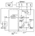
以下、本発明の実施の形態について添付図面を参照しながら説明する。図1は本発明に係る半導体集積回路の電源制御システムの一例の構成図である。同図を参照すると、本発明に係る半導体集積回路の電源制御システムの一例は、電源制御装置1と、電圧源(VRM)2と、LSIパッケージ(PKG)3と、LSI4と、プログラム格納部5とを含んで構成される。
Hereinafter, embodiments of the present invention will be described with reference to the accompanying drawings. FIG. 1 is a block diagram of an example of a power supply control system for a semiconductor integrated circuit according to the present invention. Referring to the figure, an example of a power supply control system for a semiconductor integrated circuit according to the present invention includes a power
電源制御装置1は電圧源(VRM)2と、LSI4とを制御する。電圧源(VRM)2は可変電圧源である。LSIパッケージ(PKG)3は電源配線のインダクタンス31(インダクタンス値を“L_PKG”と表示する)を含んでいる。LSI4は可変抵抗41(抵抗値を“R_DIE”と表示する)と、電圧センサー42と、内部素子43とを含んでいる。また、内部素子43は電流源43a(電流値を“I_DIE”と表示する)と、容量43b(容量値を“C_DIE”と表示する)とを含んでいる。
The power
電圧源(VRM)2の陽極はインダクタンス31の一方の端子と接続され、インダクタンス31の他方の端子は可変抵抗41の一方の端子と接続される。可変抵抗41の他方の端子は電圧センサー42の一方の入力端子および内部素子43内の後述する端子と接続される。 The anode of the voltage source (VRM) 2 is connected to one terminal of the inductance 31, and the other terminal of the inductance 31 is connected to one terminal of the variable resistor 41. The other terminal of the variable resistor 41 is connected to one input terminal of the voltage sensor 42 and a terminal to be described later in the internal element 43.
内部素子43は電流源43aと容量43bとが並列接続された回路であり、この並列接続回路の一方の接続端子と可変抵抗41の他方の端子とが接続される。この接続点にてLSI4内の電源電圧(電圧値を“V_DIE”と表示する)が観測される。並列接続回路の他方の接続端子と電圧源(VRM)2の陰極とが接続される。 The internal element 43 is a circuit in which a current source 43a and a capacitor 43b are connected in parallel, and one connection terminal of the parallel connection circuit and the other terminal of the variable resistor 41 are connected. At this connection point, the power supply voltage in the LSI 4 (the voltage value is displayed as “V_DIE”) is observed. The other connection terminal of the parallel connection circuit and the cathode of the voltage source (VRM) 2 are connected.
また、電源制御装置1は電圧制御信号(V_SET)で電圧源(VRM)2を制御し、可変抵抗制御信号(R_SET)で可変抵抗41を制御する。また、電源制御装置1は基準電圧信号(VMIN)を電圧センサー42の他方の入力端子へ出力し、電圧センサー42は電圧の比較結果情報(V_MON)を電源制御装置1へ出力する。
The power
プログラム格納部5には後述する電源制御方法のプログラムが格納されている。
The
電圧源(VRM)2と、インダクタンス31と、可変抵抗41と、内部素子43内の電流源43aおよび容量43bによる並列接続回路とで閉回路が構成される。また、この閉回路のインダクタンス31と容量43bとで並列共振回路が形成され、並列共振した場合はその並列共振信号が電源ノイズの発生源となる。 The voltage source (VRM) 2, the inductance 31, the variable resistor 41, and the parallel connection circuit including the current source 43 a and the capacitor 43 b in the internal element 43 constitute a closed circuit. In addition, a parallel resonance circuit is formed by the inductance 31 and the capacitor 43b of this closed circuit, and when parallel resonance occurs, the parallel resonance signal becomes a source of power supply noise.
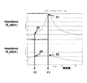
図2は可変抵抗41の抵抗値を変化させた場合のLSI4内の内部素子43から見たインピーダンスの一例を示す図である。同図にて横軸はLSI4内の内部素子43を流れる信号の周波数(Hz),縦軸はLSI内の内部素子から見たインピーダンス(Ω)を示す。 FIG. 2 is a diagram showing an example of impedance viewed from the internal element 43 in the LSI 4 when the resistance value of the variable resistor 41 is changed. In the figure, the horizontal axis represents the frequency (Hz) of the signal flowing through the internal element 43 in the LSI 4 and the vertical axis represents the impedance (Ω) viewed from the internal element in the LSI.
同図に示すように、LSI4内の内部素子43から見たインピーダンスは、図1のLSIパッケージ(PKG)3内のインダクタンス31の値(L_PKG)とLSI内の内部素子43の容量43bの値(C_DIE)とによる並列共振により、共振周波数にピークを持つ。共振周波数付近の周波数F1でのインピーダンスはR_DIEが小さいときはZ1,R_DIEが大きいときはZ2となり、Z1>Z2であり、R_DIEを大きくすることでインピーダンスを小さくすることが可能である。 As shown in the figure, the impedance viewed from the internal element 43 in the LSI 4 is the value of the inductance 31 (L_PKG) in the LSI package (PKG) 3 in FIG. 1 and the value of the capacitance 43b of the internal element 43 in the LSI ( C_DIE) has a peak at the resonance frequency due to parallel resonance. The impedance at the frequency F1 near the resonance frequency is Z1 when R_DIE is small, and Z2 when R_DIE is large. Z1> Z2, and it is possible to reduce the impedance by increasing R_DIE.
ところが、周波数F2のように共振周波数から離れた周波数では、インピーダンスはR_DIEが小さいときはZ3,R_DIEが大きいときはZ4となり、Z3<Z4であり、R_DIEを大きくするとインピーダンスは大きくなってしまう。 However, at a frequency far from the resonance frequency such as frequency F2, the impedance is Z3 when R_DIE is small and Z4 when R_DIE is large, and Z3 <Z4. When R_DIE is increased, the impedance becomes large.
本発明の電源制御システムでは、実際にLSI4を動作させた状態で、電源電圧をLSI4内の電圧センサー42でモニターし、R_DIEの値を変えることでLSI4内の電源インピーダンスを制御し、LSI4の電圧源(VRM)2の設定値を最適化することが可能となる。 In the power supply control system of the present invention, the power supply voltage is monitored by the voltage sensor 42 in the LSI 4 while the LSI 4 is actually operated, and the power impedance in the LSI 4 is controlled by changing the value of R_DIE. The set value of the source (VRM) 2 can be optimized.
次に、本電源制御システムの動作の一例について具体的に説明する。図3はLSI4内の内部素子43の消費電流(I_DIE)の周波数成分F1が共振周波数に近い場合の電圧源2の電圧(電圧値を“V_VRM”と表示する)、LSI4の電源電圧(電圧値を“V_DIE”と表示する)、可変抵抗41の抵抗(R_DIE)のシミュレーション結果、図4はLSI4内の内部素子43の消費電流(I_DIE)の周波数成分F2が共振周波数から離れた場合の電圧源2の電圧(電圧値を“V_VRM”と表示する)、LSI4の出力電圧(V_DIE)、可変抵抗41の抵抗(R_DIE)のシミュレーション結果、図5は本発明に係る電源制御システムの動作の一例を示すフローチャートをそれぞれ示している。
Next, an example of the operation of the power supply control system will be specifically described. 3 shows the voltage of the
まず、内部素子43の消費電流(I_DIE)の周波数成分F1が共振周波数に近い場合について説明する。 First, the case where the frequency component F1 of the consumption current (I_DIE) of the internal element 43 is close to the resonance frequency will be described.
図3は、図1に示す電源制御回路1の出力信号(V_SET)によりLSI4に電源を供給する電圧源(VRM)2の出力を電源の高い設定値から下げていき、LSI4内の電源電圧(V_DIE)が電源制御回路1の出力信号により設定された基準電圧(VMIN)になったときに、電圧センサー42の出力信号を電源制御回路1の入力信号(V_MON)で観測することで電圧制御信号の設定値(V_SET)を決定することを示している。
3 decreases the output of the voltage source (VRM) 2 that supplies power to the LSI 4 from the high power supply set value by the output signal (V_SET) of the power
図1に示す電源制御回路1の出力信号(R_SET)により、LSI4内部の電源配線に挿入された可変抵抗41の抵抗値(R_DIE)を小さく設定すると、電源配線のインピーダンスは高くなり、図3に示すようにV_DIE(R_DIE小)の振幅は小さくなるため、電源電圧(V_VRM)はVRM1に設定される。
When the resistance value (R_DIE) of the variable resistor 41 inserted in the power supply wiring inside the LSI 4 is set small by the output signal (R_SET) of the power
次に、電源制御回路1の出力信号(R_SET)により、LSI4内部の電源配線に挿入された可変抵抗41の抵抗値(R_DIE)を大きく設定すると、電源配線のインピーダンスは小さくなり、図3に示すようにV_DIE(R_DIE大)の振幅は大きくなるため、電源電圧(V_VRM)はVRM2に設定される。
Next, when the resistance value (R_DIE) of the variable resistor 41 inserted in the power supply wiring inside the LSI 4 is set to be large by the output signal (R_SET) of the power
すなわち、VRM1>VRM2であり、LSI4内内部素子43の消費電流(I_DIE)の周波数成分が共振周波数に近い場合(図5のステップS1にて“Y”の場合)、電源制御回路1の出力信号(R_SET)により、LSI4内部の電源配線に挿入された可変抵抗41の抵抗値(R_DIE)を大きく設定し(図5のステップS2)、電圧センサー42の出力が零となるように電圧源(VRM)の電圧を制御すると(図5のステップS3)、LSI4に電源を供給する電圧源(VRM)の出力電圧(V_VRM)を小さい値(VRM2)に設定することが可能となる。
That is, when VRM1> VRM2 and the frequency component of the current consumption (I_DIE) of the internal element 43 in the LSI 4 is close to the resonance frequency (“Y” in step S1 in FIG. 5), the output signal of the power
次に、内部素子43の消費電流(I_DIE)の周波数成分F2が共振周波数から離れた場合について説明する。 Next, the case where the frequency component F2 of the consumption current (I_DIE) of the internal element 43 is away from the resonance frequency will be described.
図4は、図1に示す電源制御回路1の出力信号(V_SET)によりLSI4に電源を供給する電圧源(VRM)2の出力を電源の高い設定値から下げていき、LSI4内の電源電圧(V_DIE)が電源制御回路1の出力信号により設定された基準電圧(VMIN)になったときに、電圧センサー42の出力信号を電源制御回路1の入力信号(V_MON)で観測することで電圧制御信号の設定値(V_SET)を決定することを示している。
4 decreases the output of the voltage source (VRM) 2 that supplies power to the LSI 4 from the high power supply set value by the output signal (V_SET) of the power
図1に示す電源制御回路1の出力信号(R_SET)により、LSI4内部の電源配線に挿入された可変抵抗41の抵抗値(R_DIE)を小さく設定すると、電源配線のインピーダンスは小さくなり、図4に示すようにV_DIE(R_DIE小)の振幅は小さくなるため、電源電圧(V_VRM)はVRM3に設定される。
When the resistance value (R_DIE) of the variable resistor 41 inserted in the power supply wiring inside the LSI 4 is set to be small by the output signal (R_SET) of the power
次に、電源制御回路1の出力信号(R_SET)により、LSI4内部の電源配線に挿入された可変抵抗41の抵抗値(R_DIE)を大きく設定すると、電源配線のインピーダンスは大きくなり、図4に示すようにV_DIE(R_DIE大)の振幅は大きくなるため、電源電圧(V_VRM)はVRM4に設定される。
Next, when the resistance value (R_DIE) of the variable resistor 41 inserted in the power supply wiring inside the LSI 4 is set large by the output signal (R_SET) of the power
すなわち、VRM3<VRM4であり、LSI4内内部素子43の消費電流(I_DIE)の周波数成分が共振周波数からはなれた場合(図5のステップS1にて“N”の場合)、電源制御回路1の出力信号(R_SET)により、LSI4内部の電源配線に挿入された可変抵抗41の抵抗値(R_DIE)を小さく設定し(図5のステップS4)、電圧センサー42の出力が零となるように電圧源(VRM)の電圧を制御すると(図5のステップS3)、LSI4に電源を供給する電圧源(VRM)の出力電圧(V_VRM)を小さい値(VRM3)に設定することが可能となる。
That is, when VRM3 <VRM4 and the frequency component of the current consumption (I_DIE) of the internal element 43 in the LSI 4 deviates from the resonance frequency (in the case of “N” in step S1 in FIG. 5), the output of the power
以上説明したように、本発明に係る電源制御システムによれば、LSI4内の電源配線のインピーダンスを最適化することで電源電圧を下げることが可能となり、これにより消費電力を低減することができるとともに、電源ノイズ振幅を抑えることでシステムの高信頼性化が可能となる。 As described above, according to the power supply control system of the present invention, it is possible to reduce the power supply voltage by optimizing the impedance of the power supply wiring in the LSI 4, thereby reducing the power consumption. By suppressing power supply noise amplitude, the system can be made highly reliable.
なお、可変抵抗41はMOS(Metal Oxide Semiconductor )素子の並列数を可変にすることでLSIで容易に構成することが可能である。 The variable resistor 41 can be easily configured by an LSI by changing the parallel number of MOS (Metal Oxide Semiconductor) elements.
次に、電源制御方法のプログラムについて説明する。図1に示すように、本発明に係る電源制御システムはプログラム格納部5を含んでいる。プログラム格納部5には図5にフローチャートで示す電源制御方法のプログラムが格納されている。電源制御回路1は、プログラム格納部5からそのプログラムを読み出し、そのプログラムにしたがって電圧源(VRM)2、可変抵抗41、電圧センサー42を制御する。その制御の内容については既に述べたので、ここでの説明は省略する。
Next, a program for the power supply control method will be described. As shown in FIG. 1, the power supply control system according to the present invention includes a
以上説明したように、本発明に係る電源制御方法のプログラムによれば、LSI4内の電源配線のインピーダンスを最適化することで電源電圧を下げることが可能となり、これにより消費電力を低減することができるとともに、電源ノイズ振幅を抑えることでシステムの高信頼性化が可能な電源制御方法のプログラムが得られる。 As described above, according to the program of the power supply control method according to the present invention, it is possible to reduce the power supply voltage by optimizing the impedance of the power supply wiring in the LSI 4, thereby reducing the power consumption. In addition, it is possible to obtain a program of a power supply control method capable of improving the reliability of the system by suppressing the power supply noise amplitude.
1 電源制御装置
2 電圧源(VRM)
3 LSIパッケージ(PKG)
4 LSI
5 プログラム格納部
31 インダクタンス
41 可変抵抗
42 電圧センサー
43 内部素子
43a 電流源
43b 容量
1 Power
3 LSI package (PKG)
4 LSI
5 Program storage unit 31 Inductance 41 Variable resistance 42 Voltage sensor 43 Internal element 43a Current source 43b Capacity
Claims (9)
前記可変電圧源から電源が供給される半導体集積回路と、
前記可変電圧源を制御する電源制御回路とを含み、
前記半導体集積回路は、インダクタンスと内部素子容量とから構成される並列共振回路と、前記並列共振回路の電源配線上に設けられる可変抵抗と、前記可変電圧源から前記並列共振回路に供給される電圧と基準電圧とを比較しその比較結果を出力する電圧センサーとを含んでおり、
前記電源制御回路は、前記電源配線に流れる信号の周波数に応じて前記可変抵抗の値を選択し、前記電圧センサーの出力結果に応じて前記可変電圧源に所定の電圧値を設定することを特徴とする半導体集積回路の電源制御システム。 A variable voltage source;
A semiconductor integrated circuit to which power is supplied from the variable voltage source;
A power supply control circuit for controlling the variable voltage source,
The semiconductor integrated circuit includes a parallel resonant circuit including an inductance and an internal element capacitance, a variable resistor provided on a power supply wiring of the parallel resonant circuit, and a voltage supplied from the variable voltage source to the parallel resonant circuit. And a voltage sensor that compares the reference voltage and outputs the comparison result,
The power supply control circuit selects a value of the variable resistor according to a frequency of a signal flowing through the power supply wiring, and sets a predetermined voltage value to the variable voltage source according to an output result of the voltage sensor. A power supply control system for semiconductor integrated circuits.
前記電源配線に流れる信号の周波数が前記並列共振回路の並列共振周波数に近い場合は、前記可変抵抗の値として第1値を選択し、前記電圧センサーから出力される電圧差が零となるように前記可変電圧源の電圧を制御するとともに、
前記電源配線に流れる信号の周波数が前記並列共振回路の並列共振周波数よりも離れている場合は、前記可変抵抗の値として前記第1値よりも小さい第2値を選択し、前記電圧センサーから出力される電圧差が零となるように前記可変電圧源の電圧を制御することを特徴とする請求項1記載の電源制御システム。 The power supply control circuit
When the frequency of the signal flowing through the power supply wiring is close to the parallel resonance frequency of the parallel resonance circuit, the first value is selected as the value of the variable resistor so that the voltage difference output from the voltage sensor becomes zero. Controlling the voltage of the variable voltage source;
When the frequency of the signal flowing through the power supply wiring is farther than the parallel resonance frequency of the parallel resonance circuit, a second value smaller than the first value is selected as the value of the variable resistor, and output from the voltage sensor The power supply control system according to claim 1, wherein the voltage of the variable voltage source is controlled so that a voltage difference to be zero becomes zero.
前記半導体集積回路パッケージに前記インダクタンスが設けられ、前記半導体集積回路本体に前記内部素子容量と前記可変抵抗と前記電圧センサーとが設けられることを特徴とする請求項1または2記載の電源制御システム。 The semiconductor integrated circuit includes a semiconductor integrated circuit package and a semiconductor integrated circuit body,
The power supply control system according to claim 1, wherein the inductance is provided in the semiconductor integrated circuit package, and the internal element capacitance, the variable resistor, and the voltage sensor are provided in the semiconductor integrated circuit main body.
前記電源制御回路は、前記電源配線に流れる信号の周波数に応じて前記可変抵抗の値を選択し、前記電圧センサーの出力結果に応じて前記可変電圧源に所定の電圧値を設定することを特徴とする電源制御方法。 A variable voltage source; a semiconductor integrated circuit to which power is supplied from the variable voltage source; and a power supply control circuit for controlling the variable voltage source. The semiconductor integrated circuit includes an inductance and an internal element capacitance. A parallel resonance circuit; a variable resistor provided on a power supply wiring of the parallel resonance circuit; a voltage sensor that compares a voltage supplied from the variable voltage source to the parallel resonance circuit with a reference voltage and outputs a comparison result; A power supply control method for a power supply control system of a semiconductor integrated circuit including:
The power supply control circuit selects a value of the variable resistor according to a frequency of a signal flowing through the power supply wiring, and sets a predetermined voltage value to the variable voltage source according to an output result of the voltage sensor. Power control method.
前記電源配線に流れる信号の周波数が前記並列共振回路の並列共振周波数に近い場合は、前記可変抵抗の値として第1値を選択し、前記電圧センサーから出力される電圧差が零となるように前記可変電圧源の電圧を制御するとともに、
前記電源配線に流れる信号の周波数が前記並列共振回路の並列共振周波数よりも離れている場合は、前記可変抵抗の値として前記第1値よりも小さい第2値を選択し、前記電圧センサーから出力される電圧差が零となるように前記可変電圧源の電圧を制御することを特徴とする請求項5記載の電源制御方法。 The power supply control circuit
When the frequency of the signal flowing through the power supply wiring is close to the parallel resonance frequency of the parallel resonance circuit, the first value is selected as the value of the variable resistor so that the voltage difference output from the voltage sensor becomes zero. Controlling the voltage of the variable voltage source;
When the frequency of the signal flowing through the power supply wiring is farther than the parallel resonance frequency of the parallel resonance circuit, a second value smaller than the first value is selected as the value of the variable resistor, and output from the voltage sensor 6. The power supply control method according to claim 5, wherein the voltage of the variable voltage source is controlled so that a voltage difference to be zero becomes zero.
前記半導体集積回路パッケージに前記インダクタンスが設けられ、前記半導体集積回路本体に前記内部素子容量と前記可変抵抗と前記電圧センサーとが設けられることを特徴とする請求項5または6記載の電源制御方法。 The semiconductor integrated circuit includes a semiconductor integrated circuit package and a semiconductor integrated circuit body,
The power supply control method according to claim 5 or 6, wherein the inductance is provided in the semiconductor integrated circuit package, and the internal element capacitance, the variable resistor, and the voltage sensor are provided in the semiconductor integrated circuit body.
前記電源制御回路に、前記電源配線に流れる信号の周波数に応じて前記可変抵抗の値を選択し、前記電圧センサーの出力結果に応じて前記可変電圧源に所定の電圧値を設定する処理を実行させるためのプログラム。 A variable voltage source; a semiconductor integrated circuit to which power is supplied from the variable voltage source; and a power supply control circuit for controlling the variable voltage source. The semiconductor integrated circuit includes an inductance and an internal element capacitance. A parallel resonance circuit; a variable resistor provided on a power supply wiring of the parallel resonance circuit; a voltage sensor that compares a voltage supplied from the variable voltage source to the parallel resonance circuit with a reference voltage and outputs a comparison result; A program of a power supply control method for a power supply control system of a semiconductor integrated circuit including:
In the power supply control circuit, the value of the variable resistor is selected according to the frequency of the signal flowing through the power supply wiring, and a predetermined voltage value is set in the variable voltage source according to the output result of the voltage sensor Program to let you.
Priority Applications (1)
| Application Number | Priority Date | Filing Date | Title |
|---|---|---|---|
| JP2011050913A JP5691670B2 (en) | 2011-03-09 | 2011-03-09 | Power supply control system and power supply control method for semiconductor integrated circuit |
Applications Claiming Priority (1)
| Application Number | Priority Date | Filing Date | Title |
|---|---|---|---|
| JP2011050913A JP5691670B2 (en) | 2011-03-09 | 2011-03-09 | Power supply control system and power supply control method for semiconductor integrated circuit |
Publications (2)
| Publication Number | Publication Date |
|---|---|
| JP2012190862A true JP2012190862A (en) | 2012-10-04 |
| JP5691670B2 JP5691670B2 (en) | 2015-04-01 |
Family
ID=47083747
Family Applications (1)
| Application Number | Title | Priority Date | Filing Date |
|---|---|---|---|
| JP2011050913A Expired - Fee Related JP5691670B2 (en) | 2011-03-09 | 2011-03-09 | Power supply control system and power supply control method for semiconductor integrated circuit |
Country Status (1)
| Country | Link |
|---|---|
| JP (1) | JP5691670B2 (en) |
Cited By (4)
| Publication number | Priority date | Publication date | Assignee | Title |
|---|---|---|---|---|
| JP2015135857A (en) * | 2014-01-16 | 2015-07-27 | 株式会社メガチップス | Power supply impedance optimization device |
| WO2015156940A3 (en) * | 2014-04-10 | 2015-12-23 | Qualcomm Incorporated | Die with resistor switch having an adjustable resistance |
| CN107017855A (en) * | 2015-10-14 | 2017-08-04 | 联发科技股份有限公司 | The method of the optimization resistance value of conductor integrated circuit device and setting damper |
| US9979597B2 (en) | 2014-04-04 | 2018-05-22 | Qualcomm Incorporated | Methods and apparatus for assisted radio access technology self-organizing network configuration |
-
2011
- 2011-03-09 JP JP2011050913A patent/JP5691670B2/en not_active Expired - Fee Related
Cited By (9)
| Publication number | Priority date | Publication date | Assignee | Title |
|---|---|---|---|---|
| JP2015135857A (en) * | 2014-01-16 | 2015-07-27 | 株式会社メガチップス | Power supply impedance optimization device |
| US9979597B2 (en) | 2014-04-04 | 2018-05-22 | Qualcomm Incorporated | Methods and apparatus for assisted radio access technology self-organizing network configuration |
| US10791027B2 (en) | 2014-04-04 | 2020-09-29 | Qualcomm Incorporated | Methods and apparatus for assisted radio access technology self-organizing network configuration |
| WO2015156940A3 (en) * | 2014-04-10 | 2015-12-23 | Qualcomm Incorporated | Die with resistor switch having an adjustable resistance |
| US9377804B2 (en) | 2014-04-10 | 2016-06-28 | Qualcomm Incorporated | Switchable package capacitor for charge conservation and series resistance |
| CN106170739A (en) * | 2014-04-10 | 2016-11-30 | 高通股份有限公司 | Tube core with the resistor switch with adjustable resistance |
| US9618957B2 (en) | 2014-04-10 | 2017-04-11 | Qualcomm Incorporated | Switchable package capacitor for charge conservation and series resistance |
| CN106170739B (en) * | 2014-04-10 | 2017-10-13 | 高通股份有限公司 | Tube core with the resistor switch with adjustable resistance |
| CN107017855A (en) * | 2015-10-14 | 2017-08-04 | 联发科技股份有限公司 | The method of the optimization resistance value of conductor integrated circuit device and setting damper |
Also Published As
| Publication number | Publication date |
|---|---|
| JP5691670B2 (en) | 2015-04-01 |
Similar Documents
| Publication | Publication Date | Title |
|---|---|---|
| JP5864220B2 (en) | Semiconductor integrated circuit | |
| CN103988422B (en) | Voltage-controlled oscillator with the single-ended electric capacity for reducing | |
| JP5691670B2 (en) | Power supply control system and power supply control method for semiconductor integrated circuit | |
| JP5241193B2 (en) | Semiconductor integrated circuit device | |
| US9843269B2 (en) | Switching power supply circuit control method | |
| JP2010191885A (en) | Voltage regulator | |
| TWI741061B (en) | Switching regulator synchronous node snubber circuit | |
| TWI665542B (en) | Voltage Regulator | |
| JP2017200385A (en) | Dc/dc converter | |
| JP2018106591A (en) | Semiconductor device, operation control method, and program | |
| JP6232232B2 (en) | Semiconductor device and current amount control method | |
| TWI439030B (en) | Soft start circuit and driving method thereof | |
| CN100539403C (en) | Electron-amplifier | |
| JP3739006B1 (en) | Power supply device and portable device | |
| JP4799651B2 (en) | Design support apparatus and design support method | |
| JP6253481B2 (en) | Voltage regulator and manufacturing method thereof | |
| JP2015027198A (en) | Semiconductor integrated circuit and power source management system | |
| JP6292325B1 (en) | Semiconductor integrated circuit, semiconductor system and method | |
| JP2009105221A (en) | Semiconductor integrated circuit device | |
| JP6138426B2 (en) | Switch circuit and igniter | |
| JP2008103808A (en) | Crystal oscillator | |
| JP4833455B2 (en) | Constant voltage generation circuit and semiconductor device | |
| JP2010041449A (en) | Oscillation circuit | |
| JP2006313493A (en) | Power supply circuit | |
| JP2012157151A (en) | Power supply unit and electronic apparatus using the same |
Legal Events
| Date | Code | Title | Description |
|---|---|---|---|
| RD04 | Notification of resignation of power of attorney |
Free format text: JAPANESE INTERMEDIATE CODE: A7424 Effective date: 20131112 |
|
| A621 | Written request for application examination |
Free format text: JAPANESE INTERMEDIATE CODE: A621 Effective date: 20140213 |
|
| TRDD | Decision of grant or rejection written | ||
| A977 | Report on retrieval |
Free format text: JAPANESE INTERMEDIATE CODE: A971007 Effective date: 20141225 |
|
| A01 | Written decision to grant a patent or to grant a registration (utility model) |
Free format text: JAPANESE INTERMEDIATE CODE: A01 Effective date: 20150106 |
|
| A61 | First payment of annual fees (during grant procedure) |
Free format text: JAPANESE INTERMEDIATE CODE: A61 Effective date: 20150119 |
|
| R150 | Certificate of patent or registration of utility model |
Ref document number: 5691670 Country of ref document: JP Free format text: JAPANESE INTERMEDIATE CODE: R150 |
|
| LAPS | Cancellation because of no payment of annual fees |