JP2009105221A - Semiconductor integrated circuit device - Google Patents
Semiconductor integrated circuit device Download PDFInfo
- Publication number
- JP2009105221A JP2009105221A JP2007275516A JP2007275516A JP2009105221A JP 2009105221 A JP2009105221 A JP 2009105221A JP 2007275516 A JP2007275516 A JP 2007275516A JP 2007275516 A JP2007275516 A JP 2007275516A JP 2009105221 A JP2009105221 A JP 2009105221A
- Authority
- JP
- Japan
- Prior art keywords
- power supply
- power
- circuit
- semiconductor integrated
- integrated circuit
- Prior art date
- Legal status (The legal status is an assumption and is not a legal conclusion. Google has not performed a legal analysis and makes no representation as to the accuracy of the status listed.)
- Pending
Links
Images


Classifications
-
- G—PHYSICS
- G11—INFORMATION STORAGE
- G11C—STATIC STORES
- G11C5/00—Details of stores covered by group G11C11/00
- G11C5/14—Power supply arrangements, e.g. power down, chip selection or deselection, layout of wirings or power grids, or multiple supply levels
- G11C5/143—Detection of memory cassette insertion or removal; Continuity checks of supply or ground lines; Detection of supply variations, interruptions or levels ; Switching between alternative supplies
Abstract
Description
本発明にかかる半導体集積回路装置は、特に電源スイッチによる電源制御が行なわれる半導体集積回路装置に関する。 The semiconductor integrated circuit device according to the present invention particularly relates to a semiconductor integrated circuit device in which power control is performed by a power switch.
近年、半導体集積回路装置では、消費電力を低減するために、使用状態に応じて内部回路の全部又は一部の動作の切り替え(例えば、内部回路における動作状態と停止状態を切り替える)が行なわれる。また、内部回路を構成するトランジスタの小型化及び消費電力の低減を目的として動作電源電圧の定電圧化が進んでいる。このような半導体集積回路装置においては、内部回路の動作の切り替えに応じて消費電流が変動する。このような消費電流の変動が生じた場合、半導体集積回路装置のパッケージあるいは内部回路に寄生する抵抗成分、コンデンサ成分、インダクタンス成分に起因して電源電圧にノイズが発生する。近年の動作電源電圧が低電圧化された半導体集積回路装置では、このノイズによる電源電圧変動によって回路に誤動作が生じる問題が顕著になってきている。 In recent years, in a semiconductor integrated circuit device, in order to reduce power consumption, operation of all or part of an internal circuit is switched (for example, switching between an operation state and a stop state in the internal circuit) according to a use state. In addition, the operation power supply voltage has been made constant for the purpose of downsizing the transistors constituting the internal circuit and reducing power consumption. In such a semiconductor integrated circuit device, current consumption fluctuates in accordance with switching of the operation of the internal circuit. When such fluctuations in current consumption occur, noise is generated in the power supply voltage due to resistance components, capacitor components, and inductance components parasitic on the package or internal circuit of the semiconductor integrated circuit device. In semiconductor integrated circuit devices in which the operating power supply voltage has been lowered in recent years, the problem of malfunction in the circuit due to fluctuations in the power supply voltage due to noise has become prominent.
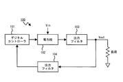
ここで、電源電圧の変動を抑制する技術として、電源電圧等の電圧を出力するレギュレータにおいて出力電圧のノイズを抑制する技術が特許文献1(以下、従来例1と称す)に開示されている。従来例1において開示されている出力レギュレータ100のブロック図を図15に示す。また、出力レギュレータ100の出力電圧Voutの変動を示すグラフを図16に示す。出力レギュレータ100は、出力電圧Voutが一定となるように負荷に電流を流す。このとき、出力レギュレータ100では、出力電圧Voutが出力センサ104を介してデジタルコントローラ101にフィードバックされる。そして、デジタルコントローラ101が出力電圧Voutの変動に応じて電力段102を制御する。また、電力段102の出力は出力フィルタ103を介して出力電圧Voutとなる。
Here, as a technique for suppressing fluctuations in the power supply voltage, a technique for suppressing noise in the output voltage in a regulator that outputs a voltage such as a power supply voltage is disclosed in Patent Document 1 (hereinafter referred to as Conventional Example 1). A block diagram of the
出力レギュレータ100では、デジタルコントローラ101に複数の電圧範囲(図16中のVL1−VH1、VL2−VH2、VL3−VH3)が予め設定されている。そして、デジタルコントローラ101は、出力電圧Voutが、最終的に最も狭い範囲となるVL1−VH1の範囲内にある電圧値V0に収束するように電力段102を制御する(図16参照)。これによって、出力レギュレータ101は、出力電圧Voutの変動を抑制している。この動作は一般的なレギュレータ動作に相当する。
In the
また、消費電流の変動に起因するノイズ及びノイズの低減方法が非特許文献1(以下、従来例2と称す)に開示されている。従来例2では、内部回路(ロジック回路)に動作電流を供給するパワーゲートスイッチの導通状態を動作電流の変動に応じて制御することで、電源ノイズを抑制している。
しかしながら、従来例1は、出力レギュレータ100の出力電圧の変動を抑制するものである。そのため、従来例1は、内部回路が停止状態から動作状態に切り替わったときに他の領域で発生した電圧変動を抑制することができない問題がある。
However, Conventional Example 1 suppresses fluctuations in the output voltage of the
また、従来例2では、パワーゲートスイッチの導通状態を予め定められた順序に従って制御しているため、例えば、パッケージの寄生成分のばらつきにより、電源電圧に予め設定した変動とは異なる変動が発生した場合、その変動に対応できない問題がある。 Further, in the conventional example 2, since the conduction state of the power gate switch is controlled according to a predetermined order, for example, a variation different from the variation set in advance in the power supply voltage occurs due to variations in the parasitic components of the package. In some cases, there is a problem that cannot cope with the fluctuation.
本発明の一態様は、内部回路に電源を供給する第1及び第2の電源配線と、前記第1の電源配線と前記第2の電源配線とを接続する電源スイッチと、前記内部回路の電源ノイズを測定する電源ノイズ測定回路と、前記電源ノイズ測定回路の測定結果に基づいて前記電源スイッチの導通状態を制御する制御回路と、を有する半導体集積回路装置である。 One embodiment of the present invention includes first and second power supply wirings that supply power to an internal circuit, a power switch that connects the first power supply wiring and the second power supply wiring, and a power supply for the internal circuit A semiconductor integrated circuit device comprising: a power supply noise measurement circuit that measures noise; and a control circuit that controls a conduction state of the power switch based on a measurement result of the power supply noise measurement circuit.
本発明にかかる半導体集積回路装置は、電源ノイズ測定回路によって測定される電源ノイズの大きさに基づき電源スイッチの導通状態を制御する。これにより、本発明にかかる半導体集積回路装置は、パッケージ等の寄生成分のばらつきに関わらず、実際に発生した電源ノイズの大きさによって電源スイッチの導通状態を制御することが可能となる。 The semiconductor integrated circuit device according to the present invention controls the conduction state of the power switch based on the magnitude of the power supply noise measured by the power supply noise measurement circuit. As a result, the semiconductor integrated circuit device according to the present invention can control the conduction state of the power switch according to the magnitude of the actually generated power noise regardless of variations in parasitic components such as packages.
本発明にかかる半導体集積回路装置によれば、パッケージ等の寄生成分のばらつきに関わらず、消費電流の変動に起因する電源ノイズを低減することができる。 According to the semiconductor integrated circuit device of the present invention, it is possible to reduce power supply noise caused by fluctuations in current consumption regardless of variations in parasitic components such as packages.
実施の形態1
以下、図面を参照して本発明の実施の形態について説明する。本実施の形態にかかる半導体集積回路装置1のブロック図を図1に示す。図1に示すように、半導体集積回路装置1は、パッケージ10とパッケージ10に納められる回路形成領域11を有する。回路形成領域11は、回路形成領域Aと回路形成領域Bとを有している。回路形成領域Aには内部回路として用いられる論理回路(不図示)、電源ノイズ測定回路12a、12b、判定回路13、制御回路14、メモリ15が形成される。回路形成領域Bは、回路形成領域Aの一部に形成される領域であり、周囲に電源スイッチ16が形成される。また、回路形成領域Bには、内部回路として用いられる論理回路(不図示)と電源ノイズ測定回路17が形成される。なお、以下の説明では、半導体集積回路装置1は、外部から供給される電源電圧及び接地電圧に基づき動作するものとする。また、図示しない内部回路は、半導体集積回路装置1における機能ブロックとして設けられる回路であるものとする。
Embodiments of the present invention will be described below with reference to the drawings. A block diagram of a semiconductor integrated
電源ノイズ測定回路12a、12bは、回路形成領域Aにおける電源ノイズ及び電源電圧レベルを測定する。電源ノイズ測定回路12aは、例えば、図面上において回路形成領域Bの上側に配置され、電源ノイズ測定回路12bは、回路形成領域Bの下側に配置される。つまり、電源ノイズ測定回路12a、12bは、回路形成領域Aの異なる部分における電源電圧値及び電源ノイズを測定する。電源ノイズ測定回路17は、回路形成領域Bにおける電源ノイズ及び電源電圧レベルを測定する。
The power supply
電源ノイズ測定回路12a、12b、17として用いられる回路に特に限定はないが、例えば、"Measurement Results of On-chip IR-drop", K.Kobayashi et al., CUSTOM INTEGRATED CIRCUITS CONFERENCE, 2002, Proceedings of the IEEE 2002, volume, issue, 2002 pp.521-524(以下、非特許文献2と称す)において示されるような測定回路回路が用いられる。非特許文献2に開示される測定回路は、レベルシフタとフリップフロップ回路を有する。そして、レベルシフタで電源電圧が基準電圧以下となったことを検出し、フリップフロップで電源電圧が基準電圧以下となっている時間を測定する。つまり。非特許文献2に開示されている測定回路では、電源電圧の低下を測定することで電源ノイズの大きさを測定する。
There are no particular limitations on the circuits used as the power supply
メモリ15は、予め設定される判定電圧値及び基準電圧値を格納する。判定回路13は、判定電圧値及び基準電圧値と電源ノイズ測定回路12a、12b、17が出力する測定結果とを比較して、電源電圧の電圧レベル及び電源ノイズが所定の範囲内にあるか否かを判定する。そして判定の結果に基づき、制御信号及び終了信号を出力する。判定回路においける電圧値及び電圧レベルの判定方法についての詳細は後述する。
The
制御回路14は、判定回路13が出力する制御信号に基づき電源スイッチ16の導通状態を制御する。電源スイッチ16は、回路形成領域Bの周囲に形成される。ここで、電源スイッチ16の詳細な構成を図2に示す。図2に示すように、回路形成領域Aには、第1の電源配線VDD_Aがメッシュ状に形成される。また、回路形成領域Bは、第1の電源配線VDD_Aによって構成されるメッシュの一区画の中に形成される。そして、回路形成領域Bの周囲には第2の電源配線VDD_Bが形成される。電源スイッチ16は、第1の電源配線VDD_Aと第2の電源配線VDD_Bの間に形成され、2つの電源配線の接続を切り替える。
The
電源スイッチ16は、複数のパワーゲートスイッチSTrを有する。図2に示す例では、回路形成領域Bの各辺にそれぞれ3つのパワーゲートスイッチSTrが形成される。また、図2に示す例では、複数のパワーゲートスイッチSTrのゲートが共通の配線によって制御回路14に接続される。図2に示す例は、制御回路14は、スイッチ制御信号として連続した電圧値(以下、アナログ電圧値と称す)によってパワーゲートスイッチSTrの導通状態を制御する。パワーゲートスイッチSTrは、例えば、NMOSトランジスタであって、ゲートに供給される電圧値によってドレイン・ソース間の抵抗値を変化させる。つまり、パワーゲートスイッチSTrは、ゲートに供給される電圧値に応じてドレイン・ソース間に流すことができる電流値が変化する。
The
NMOSトランジスタにおける、ゲート・ソース間電圧と、ドレイン・ソース間電流との関係を図3に示す。図3に示すように、NMOSトランジスタは、ゲート・ソース間電圧に応じて線形領域動作と飽和領域動作とを有する。線形領域動作では、ゲート・ソース間電圧が増加し、閾値電圧を超えるとドレイン・ソース間に電流が流れ始め、ゲート・ソース間電圧の大きさに応じてドレイン・ソース間の電流値が大きく変化する。一方、線形領域動作では、ゲート・ソース間電圧が増加した場合であっても、線形領域動作ほどドレイン・ソース間の電流値は変化しない。本実施の形態では、パワーゲートスイッチSTrに与えるアナログ電圧値を線形動作範囲で変動させることで回路形成領域Bに流れ込む電流を制御する。 FIG. 3 shows the relationship between the gate-source voltage and the drain-source current in the NMOS transistor. As shown in FIG. 3, the NMOS transistor has a linear region operation and a saturation region operation in accordance with the gate-source voltage. In the linear region operation, the gate-source voltage increases, and when the threshold voltage is exceeded, current begins to flow between the drain and source, and the current value between the drain and source varies greatly depending on the magnitude of the gate-source voltage. To do. On the other hand, in the linear region operation, even when the gate-source voltage increases, the current value between the drain and the source does not change as in the linear region operation. In the present embodiment, the current flowing into the circuit formation region B is controlled by changing the analog voltage value applied to the power gate switch STr within the linear operation range.
また、電源スイッチ16の別の例を図4に示す。図4に示す例では、パワーゲートスイッチSTrが第1の電源配線VDD_A及び第2の電源配線VDD_Bに接続される構成は、図2に示す例と同じである。しかし、図4に示す例では、制御回路14は、複数のスイッチ制御信号を出力している。図4に示す例では、回路形成領域Bの各辺にそれぞれ3つのパワーゲートスイッチSTrが接続されるが、一つのスイッチ制御信号によって12個のパワーゲートスイッチSTrのうち4つが制御される。また、図4に示す例では、スイッチ制御信号はデジタル信号であり、スイッチ制御信号がロウレベルであれば、パワーゲートスイッチSTrは遮断状態となり、スイッチ制御信号がハイレベルであれば、パワーゲートスイッチSTrは導通状態(飽和領域の動作)となる。
Another example of the
ここで、半導体集積回路装置1における電源ノイズにいて説明する。電源ノイズを説明するための半導体集積回路装置1のブロック図を図5に示す。図5に示す例では、パッケージ10の中に回路形成領域11が格納されており、回路形成領域11が回路形成領域Aと回路形成領域Bとを有している。回路形成領域Aは、電源ノイズの測定箇所である。また、回路形成領域Bの周囲には電源スイッチ16が形成されている。図5に示す半導体集積回路装置1の等価回路図を図6に示す。
Here, power supply noise in the semiconductor integrated
図6に示すように、図5に示す半導体集積回路装置1は、パッケージモデルとオンチップモデルを有する等価回路によってあらわすことができる。パッケージモデルは、電源VDC、コイルL1、L2、容量C1、抵抗R1、R2を有している。電源VDCは、−端子が接地配線に接続されており、+端子に電源配線が接続される。電源配線には、コイルL1と抵抗R1が直列に接続されている。そして、電源配線は、コイルL1と抵抗R1を介してオンチップモデル側に電源電圧を伝達する。接地配線には、コイルL2と抵抗R2が直列に接続されている。そして、接地配線は、コイルL2と抵抗R2を介してオンチップモデル側に接地電圧を伝達する。また、容量C1は、接地配線と電源配線との間に接続される。
As shown in FIG. 6, the semiconductor integrated
オンチップモデルは、抵抗R3〜R6、容量C2、C3、インバータINVを有している。抵抗R3は電源配線に直列に挿入され、抵抗R4は接地配線に直列に挿入される。抵抗R3、R4のパッケージモデル側の端子の間には容量C2が接続される。なお、容量C2の両端は、後述するシミュレーションにおける電源電圧NVDD及び接地電圧NGNDの測定箇所となる。抵抗R3、R4のパッケージモデル側とは反対の端子にはインバータINVが接続される。インバータINVの出力端子は抵抗R5を介して容量C3の一端に接続される。容量C3の他端は、抵抗R6を介して接地配線に接続される。ここで、インバータINVは、入力信号Vinが入力され、入力信号Vinを反転した出力電圧Voutを出力する。また、インバータINVを介して電源配線から容量C3に流れ込む電流をioutと称す。 The on-chip model has resistors R3 to R6, capacitors C2 and C3, and an inverter INV. The resistor R3 is inserted in series with the power supply wiring, and the resistor R4 is inserted in series with the ground wiring. A capacitor C2 is connected between the terminals on the package model side of the resistors R3 and R4. Note that both ends of the capacitor C2 serve as measurement points for the power supply voltage NVDD and the ground voltage NGND in a simulation described later. The inverter INV is connected to the terminal opposite to the package model side of the resistors R3 and R4. The output terminal of the inverter INV is connected to one end of the capacitor C3 via the resistor R5. The other end of the capacitor C3 is connected to the ground wiring via the resistor R6. Here, the inverter INV receives the input signal Vin and outputs an output voltage Vout obtained by inverting the input signal Vin. A current flowing from the power supply wiring into the capacitor C3 through the inverter INV is referred to as iout.
なお、抵抗R3は回路形成領域Aにおける電源配線の等価抵抗であり、抵抗R4は回路形成領域Aにおける接地配線の等価抵抗である。容量C2は回路形成領域Aに形成される回路の等価容量であり、容量C3は回路形成領域Bに形成される回路の等価容量である。抵抗R5、R6は、電源スイッチ16の等価抵抗である。
The resistor R3 is an equivalent resistance of the power supply wiring in the circuit formation region A, and the resistor R4 is an equivalent resistance of the ground wiring in the circuit formation region A. The capacitance C2 is an equivalent capacitance of a circuit formed in the circuit formation region A, and the capacitance C3 is an equivalent capacitance of a circuit formed in the circuit formation region B. The resistors R5 and R6 are equivalent resistors of the
ここで、図6に示す等価回路のシミュレーション結果を示す。このシミュレーションでは、抵抗R1〜R6の抵抗値を1mΩとし、容量C1の容量値を5pF、容量C2、C3の容量値を10pFとし、コイルL1、L2のインダクタンスを50nHとした。また、電源スイッチ16のオン・オフの切り替わりは、入力信号Vinによって再現している。シミュレーション結果の波形を図7に示す。
Here, a simulation result of the equivalent circuit shown in FIG. 6 is shown. In this simulation, the resistance values of the resistors R1 to R6 were 1 mΩ, the capacitance value of the capacitor C1 was 5 pF, the capacitance values of the capacitors C2 and C3 were 10 pF, and the inductances of the coils L1 and L2 were 50 nH. The on / off switching of the
図7に示すように、入力信号Vinが立ち下がり、それに応じて出力信号Voutが立ち上がると、容量C3に流れ込む電流ioutが急激に増加する。そして、電流ioutは振幅を減衰させながら所定の電流値に収束する。また、電流ioutの急激な変化によって、容量C2の両端で観測される電源電圧NVDD及び接地電圧NGNDには、電源ノイズが発生する。この電源ノイズは、パッケージモデルにおける抵抗R1、R2、コイルL1、L2、容量C1によって引き起こされるものである。また、電源電圧NVDDと接地電圧NGNDとの電圧差に着目した波形の拡大図を図8に示す。図8に示すように、電流ioutが急激な増加をすることで、電源電圧NVDDと接地電圧NGNDとの電圧差は大きく変動する。本実施の形態では、この電源電圧NVDDと接地電圧NGNDとの電圧差を測定し、測定結果に応じて電源スイッチを制御することで、この電圧差の変動を抑制する。 As shown in FIG. 7, when the input signal Vin falls and the output signal Vout rises accordingly, the current iout flowing into the capacitor C3 increases rapidly. The current iout converges to a predetermined current value while the amplitude is attenuated. Further, due to a rapid change in the current iout, power supply noise is generated in the power supply voltage NVDD and the ground voltage NGND observed at both ends of the capacitor C2. This power supply noise is caused by the resistors R1 and R2, the coils L1 and L2, and the capacitor C1 in the package model. FIG. 8 shows an enlarged view of a waveform focusing on the voltage difference between the power supply voltage NVDD and the ground voltage NGND. As shown in FIG. 8, when the current iout increases rapidly, the voltage difference between the power supply voltage NVDD and the ground voltage NGND varies greatly. In the present embodiment, the voltage difference between the power supply voltage NVDD and the ground voltage NGND is measured, and the power switch is controlled according to the measurement result, thereby suppressing fluctuations in the voltage difference.
以下で、半導体集積回路装置1の動作について説明する。半導体集積回路装置1の動作を示すフローチャートを図9に示す。図9では、電源スイッチとして図4に示した回路を用いるものとする。また、図9に示す例は、回路形成領域Aの電源はすでに投入されている状態で、電源スイッチ16を導通状態とすることで、回路形成領域Bの回路を起動する場合を示すものである。
Hereinafter, the operation of the semiconductor integrated
図9に示すように、まず、制御回路14が電源スイッチ16のパワーゲートスイッチSTrを全てオンにする(ステップS1)。これによって、回路形成領域Bの回路の動作が開始される。次に、電源ノイズ測定回路17によって回路形成領域Bの電源電圧レベルを測定する(ステップS2)。そして、判定回路13によって電源ノイズ測定回路17が測定した電源電圧レベルと判定電圧値とを比較して電源電圧レベルが判定電圧値を超えたか否かを判定する(ステップS3)。
As shown in FIG. 9, the
ステップS3における判定では、回路形成領域Bが停止状態から起動状態に移行する段階であるか、起動状態から停止状態に移行する段階であるかで、用いる判定電圧値が異なる。例えば、停止状態から起動状態に移行する段階においては上側判定電圧値DHを用い、起動状態から停止状態に移行する段階においては下側判定電圧値DLを用いる。判定電圧値と電源電圧との関係を図10、11に示す。 In the determination in step S <b> 3, the determination voltage value to be used differs depending on whether the circuit formation region B is in the stage of transition from the stopped state to the activated state or the stage of transition from the activated state to the stopped state. For example, the upper determination voltage value DH is used at the stage of transition from the stop state to the startup state, and the lower determination voltage value DL is used at the stage of transition from the startup state to the stop state. The relationship between the determination voltage value and the power supply voltage is shown in FIGS.
図10は、上側判定電圧値DHと電源電圧との関係を示すものである。図10に示すように、上側判定電圧値DHは、本来到達すべき理想電源電圧よりも若干低い電圧値が設定される。そして、回路形成領域Bの回路に対する起動動作が開始され、電源電圧が上昇し、上側判定電圧を超えるまでの期間に半導体集積回路装置1は、後述するステップS3に続く制御を行なう。一方、図11は、下側判定電圧値DLと電源電圧との関係を示すものである。図11に示すように、下側判定電圧値DLは、本来到達すべき接地電圧よりも若干高い電圧値が設定される。そして、回路形成領域Bの回路に対する停止動作が開始され、電源電圧が低下し、下側判定電圧を超えるまでの期間に半導体集積回路装置1は、後述するステップS3に続く制御を行なう。
FIG. 10 shows the relationship between the upper determination voltage value DH and the power supply voltage. As shown in FIG. 10, the upper determination voltage value DH is set to a voltage value slightly lower than the ideal power supply voltage that should be reached. Then, the semiconductor integrated
なお、電源電圧の電圧レベルが判定電圧を超えた場合、半導体集積回路装置1は、判定回路13から終了信号を出力する(ステップS8)。また、終了処理において、制御回路14による電源スイッチ16の制御を停止する(ステップS9)。
If the voltage level of the power supply voltage exceeds the determination voltage, the semiconductor integrated
続いて、ステップS3において電源電圧の電圧レベルが判定電圧に未だ達していない場合の制御について説明する。ステップS3に続くステップS4では、回路形成領域Aの電源ノイズを電源ノイズ測定回路12a、12bによって測定する。そして、判定回路13によって電源ノイズ測定回路12a、12bが測定した電源ノイズの大きさと基準電圧値とを比較して電源ノイズが判定電圧値よりも大きいか否かを判定する(ステップS5)。ここで、本実施の形態では、判定電圧値は所定の範囲を示すものであって、上側基準電圧値RHと下側基準電圧値RLとを含む。この上側基準電圧値RH及び下側基準電圧値RLは、本来の電源電圧レベルを中心にして所定の範囲を設定するものである。つまり、ステップS5において用いる判定電圧値は、上側基準電圧値RH及び下側基準電圧値RLの2つの値が入力される。
Next, the control when the voltage level of the power supply voltage has not yet reached the determination voltage in step S3 will be described. In step S4 following step S3, the power supply noise in the circuit formation region A is measured by the power supply
ステップS5において、判定電圧値により定められる所定の範囲よりも電源ノイズの大きさが大きかった場合、制御回路14は、電源ノイズの大きさに応じてオフさせるパワーゲートスイッチSTrを選択する(ステップS6)。そして、制御回路14は、パワーゲートスイッチSTrをオフさせる(ステップS7)。これにより、電源スイッチ16における抵抗値が高くなるため、回路形成領域Bに流れ込む電流が減少し、回路形成領域Aにおける電流の変動が抑制されるため、回路形成領域Aにおける電源ノイズが低減される。そして、ステップS7の動作が終了した後、再度ステップS2に戻り、回路形成領域Bにおける電源レベルの測定を行なう。
If the magnitude of the power supply noise is larger than the predetermined range determined by the determination voltage value in step S5, the
一方、ステップS5において、判定電圧値により定められる所定の範囲よりも電源ノイズの大きさが小さかった場合、ステップS1に戻り、制御回路14は、全てのパワーゲートスイッチSTrをオンさせる。
On the other hand, when the magnitude of the power supply noise is smaller than the predetermined range determined by the determination voltage value in step S5, the process returns to step S1 and the
ここで、図9に示すフローチャートに従って電源スイッチ16を制御した場合における電源ノイズの変化を図12に示す。図12では、上段のグラフに電源ノイズの波形を示し、下段のグラフに制御によってオン状態となるパワーゲートスイッチSTrの個数を示した。図12に示すように、回路形成領域Bの回路の動作が開始された状態では、パワーゲートスイッチSTrは全てオン状態である。
Here, FIG. 12 shows changes in power supply noise when the
そして、電源ノイズが大きくなり電源電圧が下側基準電圧値RLを下回った場合、オンさせるパワーゲートスイッチSTrの個数を減らす(タイミングT1)。これにより、電源スイッチ16にかかる抵抗値を増加させ、回路形成領域Bに流れ込む電流を抑制することで、電源ノイズの増大を防止する。図12に示すように、本実施の形態における電源ノイズの増加は電源スイッチ16を制御しない場合に比べて小さくなる。
When the power supply noise increases and the power supply voltage falls below the lower reference voltage value RL, the number of power gate switches STr to be turned on is reduced (timing T1). Thereby, the resistance value applied to the
一方、電源ノイズが大きくなり電源電圧が上側基準電圧値RHを上回った場合も、オンさせるパワーゲートスイッチSTrの個数を減らす(タイミングT2)。これにより、電源スイッチ16にかかる抵抗値を増加させ、回路形成領域Bに流れ込む電流を抑制することで、電源ノイズの増大を防止する。図12に示すように、本実施の形態における電源ノイズの増加は電源スイッチ16を制御しない場合に比べて小さくなる。
On the other hand, when the power supply noise increases and the power supply voltage exceeds the upper reference voltage value RH, the number of power gate switches STr to be turned on is reduced (timing T2). Thereby, the resistance value applied to the
上記説明より、本実施の形態にかかる半導体集積回路装置1では、電源スイッチ16を介して電源が供給される回路形成領域Bの回路が動作する場合に、回路形成領域Aの電源ノイズの大きさを測定し、その測定結果に応じて電源スイッチ16の導通状態を制御する。このように、電源ノイズの測定結果に基づき電源スイッチを制御することで、パッケージの寄生成分のばらつきに関わらず、電源ノイズを抑制することができる。
From the above description, in the semiconductor integrated
また、本実施の形態では、回路形成領域Bにおける電源電圧の電圧レベルが判定電圧を上回った場合に判定回路が終了信号を出力する。この終了信号は、図示しない論理回路等に送信される。半導体集積回路装置1では、動作状態を回路形成領域Aに形成される回路が、この終了信号に基づき回路形成領域Bに形成される回路の動作状態を把握することができる。この終了信号を用いることで、例えば、回路形成領域Aの回路は、回路形成領域Bの回路の動作可能か否かを判断することができる。なお、終了信号を電源ノイズの大きさが所定の範囲に収束した場合に出力しても良い。
In the present embodiment, the determination circuit outputs an end signal when the voltage level of the power supply voltage in the circuit formation region B exceeds the determination voltage. This end signal is transmitted to a logic circuit (not shown). In the semiconductor integrated
さらに、本実施の形態では、測定回路による測定結果に応じて終了信号を出力できるため、終了信号が出力されるタイミングを早めることができる。終了信号が出力されるタイミングについて、測定回路を用いた場合と用いない場合との比較例を図13に示す。図13に示す例では、上段に予め設定された順序に応じて電源スイッチ16を制御した場合における終了信号の出力タイミングを示し、下段に測定回路の測定結果に応じて電源スイッチ16を制御した場合における終了信号の出力タイミングを示した。
Furthermore, in the present embodiment, since the end signal can be output according to the measurement result by the measurement circuit, the timing at which the end signal is output can be advanced. FIG. 13 shows a comparative example of when the end signal is output when the measurement circuit is used and when it is not used. In the example shown in FIG. 13, the output timing of the end signal when the
図13に示すように、予め設定された順序に応じて電源スイッチ16を制御した場合、実際には制御開始から時刻te0が経過したときに電源ノイズが収束している場合であっても、パッケージの寄生成分のばらつきを考慮して所定のマージンを設ける必要がある。従って、終了信号は、実際に電源ノイズが収束する時刻te0よりも長い時刻te1が経過した後に出力されることになる。一方、測定回路の測定結果に応じて電源スイッチ16を制御した場合(本実施の形態の場合)、上記のようなマージンは必要なく、電源ノイズの収束と同時に終了信号を出力することができる。つまり、本実施の形態における半導体集積回路装置1は、図13の上段に示す例よりも終了信号を早いタイミング(時刻te2)で出力することができる。図13では、電源ノイズの大きさに対する終了信号の出力タイミングについて説明したが、電源電圧の大きさに対して終了信号を出力する場合においても電源ノイズの場合と同様に、終了信号を出力するタイミングを早めることができる。
As shown in FIG. 13, when the
実施の形態2
実施の形態2にかかる半導体集積回路装置2は、半導体集積回路装置1を拡張するものである。半導体集積回路装置2のブロック図を図14に示す。図14に示すように、半導体集積回路装置2は、半導体集積回路装置1に対して電源ノイズ測定回路21、22、24、電源スイッチ23、回路形成領域Cが追加されている。ここで、電源ノイズ測定回路24は、回路形成領域Cの内部に形成されているものであり、電源スイッチ23は、回路形成領域Cの周囲に形成される。電源ノイズ測定回路21、22は、電源ノイズ測定回路12a、12bと同じものであり、電源スイッチ23は電源スイッチ16と同じものであり、電源ノイズ測定回路24は電源ノイズ測定回路17と同じものである。
A semiconductor integrated
つまり、実施の形態2にかかる半導体集積回路装置2は、半導体集積回路装置1に対して電源スイッチにより電源が供給される回路形成領域を増やし、かつ、回路形成領域Aにおける電源ノイズの観測点を増やしたものである。つまり、本発明は、電源スイッチによって電源が供給される回路形成領域の数に関わらず適用可能である。また、回路形成領域Aにおける観測点を増やすことで、回路形成領域全体の亘って均等に電源ノイズを低減することが可能となる。
That is, the semiconductor integrated
なお、本発明は上記実施の形態に限られたものではなく、趣旨を逸脱しない範囲で適宜変更することが可能である。例えば、測定回路については半導体集積回路装置の使用に応じて適宜変更することが可能である。 Note that the present invention is not limited to the above-described embodiment, and can be changed as appropriate without departing from the spirit of the present invention. For example, the measurement circuit can be appropriately changed according to the use of the semiconductor integrated circuit device.
1、2 半導体集積回路装置
10 パッケージ
11 回路形成領域
12a、12b、17、21、22、24 電源ノイズ測定回路
13 判定回路
14 制御回路
15 メモリ
16、23 電源スイッチ
STr パワーゲートスイッチ
VDD_A、VDD_B 電源配線
A、B、C 回路形成領域
L1、L2 コイル
C1〜C3 容量
R1〜R6 抵抗
INV インバータ
DH 上側判定電圧値
DL 下側判定電圧値
RH 上側判定電圧値
RL 下側判定電圧値
Vin 入力信号
Vout 出力信号
iout 電流
NGND 接地電圧
NVDD 電源電圧
DESCRIPTION OF
Claims (8)
前記第1の電源配線と前記第2の電源配線とを接続する電源スイッチと、
前記内部回路の電源ノイズを測定する電源ノイズ測定回路と、
前記電源ノイズ測定回路の測定結果に基づいて前記電源スイッチの導通状態を制御する制御回路と、
を有する半導体集積回路装置。 First and second power supply lines for supplying power to the internal circuit;
A power switch connecting the first power supply wiring and the second power supply wiring;
A power supply noise measuring circuit for measuring power supply noise of the internal circuit;
A control circuit for controlling the conduction state of the power switch based on the measurement result of the power noise measurement circuit;
A semiconductor integrated circuit device.
Priority Applications (2)
| Application Number | Priority Date | Filing Date | Title |
|---|---|---|---|
| JP2007275516A JP2009105221A (en) | 2007-10-23 | 2007-10-23 | Semiconductor integrated circuit device |
| US12/289,197 US20090102287A1 (en) | 2007-10-23 | 2008-10-22 | Semiconductor integrated circuit device |
Applications Claiming Priority (1)
| Application Number | Priority Date | Filing Date | Title |
|---|---|---|---|
| JP2007275516A JP2009105221A (en) | 2007-10-23 | 2007-10-23 | Semiconductor integrated circuit device |
Publications (1)
| Publication Number | Publication Date |
|---|---|
| JP2009105221A true JP2009105221A (en) | 2009-05-14 |
Family
ID=40562766
Family Applications (1)
| Application Number | Title | Priority Date | Filing Date |
|---|---|---|---|
| JP2007275516A Pending JP2009105221A (en) | 2007-10-23 | 2007-10-23 | Semiconductor integrated circuit device |
Country Status (2)
| Country | Link |
|---|---|
| US (1) | US20090102287A1 (en) |
| JP (1) | JP2009105221A (en) |
Cited By (4)
| Publication number | Priority date | Publication date | Assignee | Title |
|---|---|---|---|---|
| JP2011124339A (en) * | 2009-12-09 | 2011-06-23 | Fujitsu Ltd | Semiconductor device |
| JP2011210788A (en) * | 2010-03-29 | 2011-10-20 | Hitachi Ltd | Semiconductor device and control method therefor |
| JP2017506328A (en) * | 2014-01-16 | 2017-03-02 | クゥアルコム・インコーポレイテッドQualcomm Incorporated | Voltage-dependent die RC modeling for system-level power distribution networks |
| JP2017175371A (en) * | 2016-03-23 | 2017-09-28 | 富士通株式会社 | Electronic apparatus, power circuit and integrated circuit |
Citations (2)
| Publication number | Priority date | Publication date | Assignee | Title |
|---|---|---|---|---|
| JP2003168735A (en) * | 2001-11-30 | 2003-06-13 | Hitachi Ltd | Semiconductor integrated circuit device |
| WO2007108383A1 (en) * | 2006-03-16 | 2007-09-27 | Fujitsu Limited | Semiconductor device capable of suppressing power supply noise |
Family Cites Families (12)
| Publication number | Priority date | Publication date | Assignee | Title |
|---|---|---|---|---|
| JP3608361B2 (en) * | 1997-12-26 | 2005-01-12 | 株式会社日立製作所 | Low noise semiconductor integrated circuit device |
| US6366061B1 (en) * | 1999-01-13 | 2002-04-02 | Carnegie Mellon University | Multiple power supply circuit architecture |
| US6977492B2 (en) * | 2002-07-10 | 2005-12-20 | Marvell World Trade Ltd. | Output regulator |
| US6842027B2 (en) * | 2002-10-07 | 2005-01-11 | Intel Corporation | Method and apparatus for detection and quantification of on-die voltage noise in microcircuits |
| US6823293B2 (en) * | 2002-12-31 | 2004-11-23 | International Business Machines Corporation | Hierarchical power supply noise monitoring device and system for very large scale integrated circuits |
| JP3775416B2 (en) * | 2003-02-10 | 2006-05-17 | オムロン株式会社 | Inverter device |
| JP4158856B2 (en) * | 2003-04-17 | 2008-10-01 | 松下電器産業株式会社 | Boost power supply circuit |
| JP4223379B2 (en) * | 2003-12-10 | 2009-02-12 | 三菱電機株式会社 | Switching device control device and motor drive circuit control device |
| JP4367700B2 (en) * | 2004-03-30 | 2009-11-18 | 株式会社ルネサステクノロジ | Semiconductor integrated circuit device |
| US7126330B2 (en) * | 2004-06-03 | 2006-10-24 | Honeywell International, Inc. | Integrated three-dimensional magnetic sensing device and method to fabricate an integrated three-dimensional magnetic sensing device |
| US7355435B2 (en) * | 2005-02-10 | 2008-04-08 | International Business Machines Corporation | On-chip detection of power supply vulnerabilities |
| JP4820571B2 (en) * | 2005-04-15 | 2011-11-24 | ルネサスエレクトロニクス株式会社 | Semiconductor device |
-
2007
- 2007-10-23 JP JP2007275516A patent/JP2009105221A/en active Pending
-
2008
- 2008-10-22 US US12/289,197 patent/US20090102287A1/en not_active Abandoned
Patent Citations (2)
| Publication number | Priority date | Publication date | Assignee | Title |
|---|---|---|---|---|
| JP2003168735A (en) * | 2001-11-30 | 2003-06-13 | Hitachi Ltd | Semiconductor integrated circuit device |
| WO2007108383A1 (en) * | 2006-03-16 | 2007-09-27 | Fujitsu Limited | Semiconductor device capable of suppressing power supply noise |
Cited By (4)
| Publication number | Priority date | Publication date | Assignee | Title |
|---|---|---|---|---|
| JP2011124339A (en) * | 2009-12-09 | 2011-06-23 | Fujitsu Ltd | Semiconductor device |
| JP2011210788A (en) * | 2010-03-29 | 2011-10-20 | Hitachi Ltd | Semiconductor device and control method therefor |
| JP2017506328A (en) * | 2014-01-16 | 2017-03-02 | クゥアルコム・インコーポレイテッドQualcomm Incorporated | Voltage-dependent die RC modeling for system-level power distribution networks |
| JP2017175371A (en) * | 2016-03-23 | 2017-09-28 | 富士通株式会社 | Electronic apparatus, power circuit and integrated circuit |
Also Published As
| Publication number | Publication date |
|---|---|
| US20090102287A1 (en) | 2009-04-23 |
Similar Documents
| Publication | Publication Date | Title |
|---|---|---|
| US6876252B2 (en) | Non-abrupt switching of sleep transistor of power gate structure | |
| TWI498702B (en) | Voltage regulator | |
| JP5241193B2 (en) | Semiconductor integrated circuit device | |
| US7851948B2 (en) | Semiconductor device | |
| Andersen et al. | 20.3 A feedforward controlled on-chip switched-capacitor voltage regulator delivering 10W in 32nm SOI CMOS | |
| US7948819B2 (en) | Integrated circuit having a memory with process-voltage-temperature control | |
| JP5814876B2 (en) | Synchronous rectification type power supply circuit and adjustment method thereof | |
| JP6232232B2 (en) | Semiconductor device and current amount control method | |
| KR100813535B1 (en) | Apparatus for attenuating power noise of semiconductor integrated circuit | |
| JP2009105221A (en) | Semiconductor integrated circuit device | |
| JP5107790B2 (en) | regulator | |
| JP4713896B2 (en) | Method and apparatus for robust mode selection with low power consumption | |
| JP3989358B2 (en) | Semiconductor integrated circuit device and electronic system | |
| US8476966B2 (en) | On-die voltage regulation using p-FET header devices with a feedback control loop | |
| US7479767B2 (en) | Power supply step-down circuit and semiconductor device | |
| US7460966B1 (en) | Microcontroller that maintains capacitors of an analog circuit in a charged state during low power operation | |
| JPH0856144A (en) | Initializing circuit | |
| JP4900471B2 (en) | I / O circuit device | |
| JP7385383B2 (en) | Semiconductor devices, systems and control methods | |
| JP2011014629A (en) | Semiconductor device | |
| JP2008067323A (en) | Rush current controller and rush current control method | |
| US6118311A (en) | Output circuit capable of suppressing bounce effect | |
| JP2020174323A (en) | Semiconductor device | |
| JP2014134862A (en) | Semiconductor device | |
| JP6889047B2 (en) | Switching control circuit |
Legal Events
| Date | Code | Title | Description |
|---|---|---|---|
| A621 | Written request for application examination |
Free format text: JAPANESE INTERMEDIATE CODE: A621 Effective date: 20100512 |
|
| A977 | Report on retrieval |
Free format text: JAPANESE INTERMEDIATE CODE: A971007 Effective date: 20121128 |
|
| A02 | Decision of refusal |
Free format text: JAPANESE INTERMEDIATE CODE: A02 Effective date: 20130813 |