JP2012189571A - Semiconductor device and method of manufacturing the same - Google Patents

Semiconductor device and method of manufacturing the same Download PDF

Info

Publication number
JP2012189571A
JP2012189571A JP2011190906A JP2011190906A JP2012189571A JP 2012189571 A JP2012189571 A JP 2012189571A JP 2011190906 A JP2011190906 A JP 2011190906A JP 2011190906 A JP2011190906 A JP 2011190906A JP 2012189571 A JP2012189571 A JP 2012189571A
Authority
JP
Japan
Prior art keywords
wiring
semiconductor device
heater
gas flow
flow path
Prior art date
Legal status (The legal status is an assumption and is not a legal conclusion. Google has not performed a legal analysis and makes no representation as to the accuracy of the status listed.)
Pending
Application number
JP2011190906A
Other languages
Japanese (ja)
Inventor
Akira Tanabe
昭 田辺
Current Assignee (The listed assignees may be inaccurate. Google has not performed a legal analysis and makes no representation or warranty as to the accuracy of the list.)
Renesas Electronics Corp
Original Assignee
Renesas Electronics Corp
Priority date (The priority date is an assumption and is not a legal conclusion. Google has not performed a legal analysis and makes no representation as to the accuracy of the date listed.)
Filing date
Publication date
Application filed by Renesas Electronics Corp filed Critical Renesas Electronics Corp
Priority to JP2011190906A priority Critical patent/JP2012189571A/en
Priority to US13/396,273 priority patent/US20120217609A1/en
Priority to CN2012100448199A priority patent/CN102650648A/en
Publication of JP2012189571A publication Critical patent/JP2012189571A/en
Pending legal-status Critical Current

Links

Images

Classifications

    • GPHYSICS
    • G01MEASURING; TESTING
    • G01PMEASURING LINEAR OR ANGULAR SPEED, ACCELERATION, DECELERATION, OR SHOCK; INDICATING PRESENCE, ABSENCE, OR DIRECTION, OF MOVEMENT
    • G01P15/00Measuring acceleration; Measuring deceleration; Measuring shock, i.e. sudden change of acceleration
    • G01P15/18Measuring acceleration; Measuring deceleration; Measuring shock, i.e. sudden change of acceleration in two or more dimensions
    • GPHYSICS
    • G01MEASURING; TESTING
    • G01PMEASURING LINEAR OR ANGULAR SPEED, ACCELERATION, DECELERATION, OR SHOCK; INDICATING PRESENCE, ABSENCE, OR DIRECTION, OF MOVEMENT
    • G01P15/00Measuring acceleration; Measuring deceleration; Measuring shock, i.e. sudden change of acceleration
    • G01P15/02Measuring acceleration; Measuring deceleration; Measuring shock, i.e. sudden change of acceleration by making use of inertia forces using solid seismic masses
    • G01P15/08Measuring acceleration; Measuring deceleration; Measuring shock, i.e. sudden change of acceleration by making use of inertia forces using solid seismic masses with conversion into electric or magnetic values
    • G01P15/0897Measuring acceleration; Measuring deceleration; Measuring shock, i.e. sudden change of acceleration by making use of inertia forces using solid seismic masses with conversion into electric or magnetic values by thermal pick-up

Abstract

PROBLEM TO BE SOLVED: To solve a problem with manufacture of an acceleration sensor based on MEMS technology, where although the acceleration sensor having a complicated configuration can be obtained, a MEMS-specific process is required to be passed, thereby causing a low affinity for a normal semiconductor manufacturing process.SOLUTION: A semiconductor device 100 comprises: a laminate 10 provided with a concave gas passage 22; a heater 40 provided for the laminate 10 and exposed from the bottom of the gas passage 22; a plurality of thermal sensors 30 and 50 provided for the laminate 10, exposed from the bottom of the gas passage 22, and arranged so as to sandwich the heater 40 in the extension direction of the gas passage 22. This can provide an acceleration sensor having a high affinity for a normal semiconductor manufacturing process.

Description

本発明は、半導体装置及びその製造方法に関し、例えば、ガス式加速度センサに適用される。   The present invention relates to a semiconductor device and a manufacturing method thereof, and is applied to, for example, a gas acceleration sensor.

近年、携帯情報機器の高性能化に伴って、これらの機器に各種センサが搭載されるようになっている。加速度センサは、ゲーム機のコントローラ、携帯電話等の移動体通信端末等にとって必須のデバイスとなっている。   In recent years, as the performance of portable information devices has increased, various sensors have been mounted on these devices. The acceleration sensor is an indispensable device for a game machine controller, a mobile communication terminal such as a mobile phone.

加速度センサは、光学式、静電容量式、ピエゾ抵抗式、ガス温度分布方式等が知られている。光学式の加速度センサは、光ファイバを構成要素とするため、小型化/集積化には限界がある。他の3方式は、MEMS技術をベースとして製造される。なお、小型な電子機器に対して加速度センサを組み込む場合、MEMS(Micro Electro Mechanical Systems)技術をベースとして製造された加速度センサを用いることが一般的である。   As the acceleration sensor, an optical type, a capacitance type, a piezoresistive type, a gas temperature distribution type, and the like are known. Since an optical acceleration sensor includes an optical fiber as a component, there is a limit to miniaturization / integration. The other three systems are manufactured based on MEMS technology. When an acceleration sensor is incorporated into a small electronic device, an acceleration sensor manufactured based on MEMS (Micro Electro Mechanical Systems) technology is generally used.

特許文献1には、次の熱型加速度センサが開示されている。半導体基板上に熱分離された3本の梁を設け、中央の梁にヒータを設ける。左側の梁と中央の梁上に熱電対を設ける。同様に、右側の梁と中央の梁にも熱電対を設ける。各熱電対の起電力は、増幅器で増幅され、演算処理される。各熱電対の出力の差分を求めることで、加速度出力信号が生成される。   Patent Document 1 discloses the following thermal acceleration sensor. Three heat-isolated beams are provided on the semiconductor substrate, and a heater is provided in the central beam. A thermocouple is installed on the left beam and the central beam. Similarly, thermocouples are provided on the right beam and the central beam. The electromotive force of each thermocouple is amplified by an amplifier and processed. An acceleration output signal is generated by obtaining a difference between outputs of the thermocouples.

特許文献2にも、ガス式角速度検出器が開示されている。絶縁板に穴を設け、絶縁板の一面側にて絶縁板の穴を跨ぐように加熱ワイヤを設け、絶縁板の他面側にて絶縁板の穴を跨ぐようにヒートセンサを設ける構成が特許文献2に開示されている。   Patent Document 2 also discloses a gas angular velocity detector. A configuration in which a hole is provided in the insulating plate, a heating wire is provided so as to straddle the hole of the insulating plate on one side of the insulating plate, and a heat sensor is provided so as to straddle the hole of the insulating plate on the other side of the insulating plate. It is disclosed in Document 2.

特許文献3には、発熱体を交流駆動によって加熱することで、一組のヒータの出力波形の位相差を検知し、これに基づいて角速度を算出することが開示されている。   Patent Document 3 discloses that a heating element is heated by AC driving to detect a phase difference between output waveforms of a pair of heaters and calculate an angular velocity based on the detected phase difference.

特開2000−65850号公報JP 2000-65850 A 特開平6−27124号公報JP-A-6-27124 特開平6−174738号公報JP-A-6-174738

MEMS技術をベースとして加速度センサを製造する場合、複雑構成の加速度センサを得ることができるものの、MEMS特有の製造プロセスを経る必要があり、通常の半導体製造プロセスとの親和性は低いという問題がある。   When manufacturing an acceleration sensor based on MEMS technology, an acceleration sensor with a complicated configuration can be obtained, but it is necessary to go through a manufacturing process unique to MEMS, and there is a problem of low affinity with a normal semiconductor manufacturing process. .

本発明に係る半導体装置は、凹状のガス流路が設けられた積層体と、前記積層体に対して設けられると共に、前記ガス流路の底面にて露出する発熱部と、前記積層体に対して設けられると共に、前記ガス流路の前記底面にて露出し、かつ前記ガス流路の延在方向において前記発熱部を挟み込むように配置された複数の感温部と、を備える。   A semiconductor device according to the present invention includes a stacked body provided with a concave gas flow path, a heat generating portion that is provided on the stacked body, exposed at a bottom surface of the gas flow path, and the stacked body. And a plurality of temperature sensing parts that are exposed at the bottom surface of the gas flow path and are disposed so as to sandwich the heat generating part in the extending direction of the gas flow path.

ガス流路、発熱部及び複数の感温部を積層体に設け、ガス流路の底面にて発熱部及び複数の感温部を露出させる。これによって、通常の半導体プロセスに対して親和性が高い加速度センサを提供することが可能になる。   A gas flow path, a heat generating part, and a plurality of temperature sensitive parts are provided in the laminate, and the heat generating part and the plurality of temperature sensitive parts are exposed at the bottom of the gas flow path. As a result, it is possible to provide an acceleration sensor having high affinity for a normal semiconductor process.

本発明に係る半導体装置の製造方法は、積層体に対して発熱部を形成し、前記積層体に対して、前記発熱部を挟み込む態様にて、複数の感温部を形成し、前記発熱部及び複数の前記感温部の配置方向に沿って延在し、前記発熱部及び複数の前記感温部を底面において露出させる凹状のガス流路を設ける。   The method for manufacturing a semiconductor device according to the present invention includes forming a heat generating portion with respect to a stacked body, forming a plurality of temperature sensitive portions in a manner of sandwiching the heat generating portion with respect to the stacked body, and And a concave gas flow path extending along the arrangement direction of the plurality of temperature sensing parts and exposing the heat generating part and the plurality of temperature sensing parts on the bottom surface.

本発明によれば、通常の半導体製造プロセスに対して親和性が高い加速度センサを提供することができる。   ADVANTAGE OF THE INVENTION According to this invention, an acceleration sensor with high affinity with respect to a normal semiconductor manufacturing process can be provided.

本発明の実施の形態1にかかる半導体装置の概略的な上面図である。1 is a schematic top view of a semiconductor device according to a first embodiment of the present invention. 本発明の実施の形態1にかかる半導体装置の概略的な断面模式図である。1 is a schematic cross-sectional schematic view of a semiconductor device according to a first embodiment of the present invention. 本発明の実施の形態1にかかる半導体装置の概略的な断面模式図である。1 is a schematic cross-sectional schematic view of a semiconductor device according to a first embodiment of the present invention. 本発明の実施の形態1にかかるヒータの概略的な上面図である。It is a schematic top view of the heater concerning Embodiment 1 of this invention. 本発明の実施の形態1にかかるヒータの駆動回路を示す回路図である。It is a circuit diagram which shows the drive circuit of the heater concerning Embodiment 1 of this invention. 本発明の実施の形態1にかかる熱検出回路を示す回路図である。It is a circuit diagram which shows the heat detection circuit concerning Embodiment 1 of this invention. 本発明の実施の形態1にかかる加速度の検出原理の説明図である。It is explanatory drawing of the detection principle of the acceleration concerning Embodiment 1 of this invention. 本発明の実施の形態1にかかる加速度の検出原理の説明図である。It is explanatory drawing of the detection principle of the acceleration concerning Embodiment 1 of this invention. 本発明の実施の形態1にかかる加速度の検出構成を示すブロック図である。It is a block diagram which shows the detection structure of the acceleration concerning Embodiment 1 of this invention. 本発明の実施の形態2にかかる半導体装置の概略的な断面模式図である。FIG. 6 is a schematic cross-sectional schematic diagram of a semiconductor device according to a second embodiment of the present invention. 本発明の実施の形態2にかかる半導体装置の概略的な上面図である。It is a schematic top view of the semiconductor device concerning Embodiment 2 of this invention. 本発明の実施の形態2にかかる熱検出回路を示す回路図である。It is a circuit diagram which shows the heat detection circuit concerning Embodiment 2 of this invention. 本発明の実施の形態3にかかる熱検出回路を示す回路図である。It is a circuit diagram which shows the heat detection circuit concerning Embodiment 3 of this invention. 本発明の実施の形態3にかかる熱検出回路の動作原理を示す図である。It is a figure which shows the principle of operation of the heat detection circuit concerning Embodiment 3 of this invention. 本発明の実施の形態4にかかるヒータの駆動回路を示す回路図である。It is a circuit diagram which shows the drive circuit of the heater concerning Embodiment 4 of this invention. 本発明の実施の形態4にかかるヒータの駆動回路の動作を示すタイミングチャートである。It is a timing chart which shows operation | movement of the drive circuit of the heater concerning Embodiment 4 of this invention. 本発明の実施の形態5にかかる半導体装置の概略的な断面模式図である。FIG. 10 is a schematic cross-sectional schematic diagram of a semiconductor device according to a fifth embodiment of the present invention. 本発明の実施の形態6にかかる半導体装置の概略的な断面模式図である。FIG. 10 is a schematic cross-sectional schematic diagram of a semiconductor device according to a sixth embodiment of the present invention. 本発明の実施の形態7にかかる半導体装置の概略的な断面模式図である。It is a schematic cross-sectional schematic diagram of a semiconductor device according to a seventh embodiment of the present invention. 本発明の実施の形態8にかかる半導体装置の概略的な断面模式図である。FIG. 10 is a schematic cross-sectional schematic diagram of a semiconductor device according to an eighth embodiment of the present invention. 本発明の実施の形態9にかかるヒータを示す概略図である。It is the schematic which shows the heater concerning Embodiment 9 of this invention. 本発明の実施の形態10にかかる半導体装置の概略的な模式図である。It is a schematic model diagram of a semiconductor device according to a tenth embodiment of the present invention. 本発明の実施の形態11にかかる加速度の検出構成を示すブロック図である。It is a block diagram which shows the detection structure of the acceleration concerning Embodiment 11 of this invention. 本発明の実施の形態12にかかる半導体装置の概略的な断面模式図である。It is a schematic cross section of a semiconductor device according to a twelfth embodiment of the present invention. 本発明の実施の形態12にかかる半導体装置の概略的な断面模式図である。It is a schematic cross section of a semiconductor device according to a twelfth embodiment of the present invention. 本発明の実施の形態13にかかる半導体装置の概略的な上面模式図である。It is a schematic upper surface schematic diagram of the semiconductor device concerning Embodiment 13 of this invention. 参考例による加速度センサの概略的な模式図である。It is a schematic model diagram of the acceleration sensor by a reference example. 本発明の実施の形態14にかかる半導体装置の概略的な模式図である。It is a schematic diagram of the semiconductor device concerning Embodiment 14 of this invention. 本発明の実施の形態14にかかる半導体装置の製造方法を示す断面模式図である。It is a cross-sectional schematic diagram which shows the manufacturing method of the semiconductor device concerning Embodiment 14 of this invention. 本発明の実施の形態15にかかる半導体装置の概略的な模式図である。FIG. 17 is a schematic schematic diagram of a semiconductor device according to a fifteenth embodiment of the present invention. 本発明の実施の形態16にかかる半導体装置の概略的な模式図である。FIG. 20 is a schematic schematic diagram of a semiconductor device according to a sixteenth embodiment of the present invention. 本発明の実施の形態16にかかる半導体装置の製造方法を示す断面模式図である。It is a cross-sectional schematic diagram which shows the manufacturing method of the semiconductor device concerning Embodiment 16 of this invention. 本発明の実施の形態17にかかる半導体装置の概略的な模式図である。It is a schematic model diagram of the semiconductor device concerning Embodiment 17 of this invention. 本発明の実施の形態18にかかる半導体装置の概略的な模式図である。FIG. 20 is a schematic schematic diagram of a semiconductor device according to an eighteenth embodiment of the present invention. 本発明の実施の形態19にかかる半導体装置の概略的な模式図である。FIG. 20 is a schematic diagram of a semiconductor device according to a nineteenth embodiment of the present invention. 本発明の実施の形態20にかかる半導体装置の概略的な模式図である。FIG. 20 is a schematic diagram of a semiconductor device according to a twentieth embodiment of the present invention. 本発明の実施の形態21にかかる半導体装置の概略的な上面模式図である。FIG. 38 is a schematic top view of a semiconductor device according to a twenty-first embodiment of the present invention. 本発明の実施の形態22にかかるヒータまたは熱センサの概略的な上面模式図である。It is a schematic upper surface schematic diagram of the heater or thermal sensor concerning Embodiment 22 of this invention. 本発明の実施の形態23にかかるヒータ及び熱センサの概略的な上面模式図である。It is a schematic upper surface schematic diagram of a heater and a thermal sensor according to a twenty-third embodiment of the present invention. 本発明の実施の形態24にかかるヒータまたは熱センサの概略的な斜視図である。It is a schematic perspective view of the heater or thermal sensor concerning Embodiment 24 of this invention. 参考例による半導体装置の概略的な上面模式図である。It is a schematic upper surface schematic diagram of the semiconductor device by a reference example. 本発明の実施の形態25にかかる半導体装置の概略的な上面模式図である。FIG. 28 is a schematic top view of a semiconductor device according to a twenty-fifth embodiment of the present invention. 本発明の実施の形態25にかかる半導体装置の概略的な断面模式図である。FIG. 28 is a schematic cross-sectional view of a semiconductor device according to a twenty-fifth embodiment of the present invention. 本発明の実施の形態26にかかる半導体装置の概略的な上面模式図である。FIG. 38 is a schematic top view of a semiconductor device according to a twenty-sixth embodiment of the present invention. 本発明の実施の形態27にかかる半導体装置の概略的な上面模式図である。42 is a schematic top view of a semiconductor device according to a twenty-seventh embodiment of the present invention; FIG. 本発明の実施の形態28にかかる抵抗読み出し回路を示す回路図である。It is a circuit diagram which shows the resistance read-out circuit concerning Embodiment 28 of this invention. 本発明の実施の形態29にかかる抵抗読み出し回路を示す回路図である。FIG. 38 is a circuit diagram showing a resistance readout circuit according to a twenty-ninth embodiment of the present invention. 本発明の実施の形態29にかかる抵抗読み出し回路の概略的な断面模式図である。FIG. 34 is a schematic cross-sectional schematic diagram of a resistance readout circuit according to a twenty-ninth embodiment of the present invention. 本発明の実施の形態30にかかる抵抗読み出し回路を示す回路図である。It is a circuit diagram which shows the resistance read-out circuit concerning Embodiment 30 of this invention. 本発明の実施の形態31にかかる半導体装置の概略的な模式図である。42 is a schematic schematic diagram of a semiconductor device according to a thirty-first embodiment of the present invention; FIG. 本発明の実施の形態32にかかる半導体装置の概略的な模式図である。FIG. 38 is a schematic schematic diagram of a semiconductor device according to a thirty-second embodiment of the present invention. 本発明の実施の形態33にかかる熱検出回路を示す回路図である。It is a circuit diagram which shows the heat detection circuit concerning Embodiment 33 of this invention. 本発明の実施の形態33にかかる熱検出回路の検出原理の説明図である。It is explanatory drawing of the detection principle of the heat detection circuit concerning Embodiment 33 of this invention. 本発明の実施の形態34にかかる半導体装置の測定構成を示すブロック図である。It is a block diagram which shows the measurement structure of the semiconductor device concerning Embodiment 34 of this invention. 本発明の実施の形態34にかかる読み出し回路を示す回路図である。FIG. 38 is a circuit diagram showing a readout circuit according to a thirty-fourth embodiment of the present invention. 本発明の実施の形態34にかかる半導体装置の測定結果を示すグラフである。It is a graph which shows the measurement result of the semiconductor device concerning Embodiment 34 of this invention. 本発明の実施の形態35にかかる熱検出回路を示す回路図である。It is a circuit diagram which shows the heat detection circuit concerning Embodiment 35 of this invention. 本発明の実施の形態36にかかる熱検出回路を示す回路図である。It is a circuit diagram which shows the heat detection circuit concerning Embodiment 36 of this invention. 本発明の実施の形態37にかかる比較器を示す回路図である。It is a circuit diagram which shows the comparator concerning Embodiment 37 of this invention. 本発明の実施の形態37にかかる比較器を示す回路図である。It is a circuit diagram which shows the comparator concerning Embodiment 37 of this invention. 本発明の実施の形態37にかかる比較器を示す回路図である。It is a circuit diagram which shows the comparator concerning Embodiment 37 of this invention.

以下、図面を参照しつつ、本発明の実施形態について説明する。以降説明する各実施形態は、個々に独立したものではなく、適宜、組み合わせることが可能であり、かつ、その組み合わせの効果も主張可能なものとする。同一の要素には同一の符号を付し、重複説明は省略する。図面は、発明説明を目的として作成されたものであり、これを理由として本願発明を限定解釈することは許されない。   Hereinafter, embodiments of the present invention will be described with reference to the drawings. The embodiments described below are not individually independent but can be combined as appropriate, and the effects of the combinations can be claimed. The same elements are denoted by the same reference numerals, and redundant description is omitted. The drawings are prepared for the purpose of explaining the invention, and the invention is not allowed to be limitedly interpreted for this reason.

実施の形態1
以下、図面を参照して本発明の実施の形態について説明する。図1は、半導体装置の概略的な上面図である。図2及び図3は、半導体装置の概略的な断面模式図である。図4は、ヒータの概略的な上面図である。図5は、ヒータの駆動回路を示す回路図である。図6は、熱検出回路を示す回路図である。図7及び図8は、加速度の検出原理の説明図である。図9は、加速度の検出構成を示すブロック図である。
Embodiment 1
Embodiments of the present invention will be described below with reference to the drawings. FIG. 1 is a schematic top view of a semiconductor device. 2 and 3 are schematic cross-sectional views of the semiconductor device. FIG. 4 is a schematic top view of the heater. FIG. 5 is a circuit diagram showing a heater drive circuit. FIG. 6 is a circuit diagram showing a heat detection circuit. 7 and 8 are explanatory diagrams of the principle of acceleration detection. FIG. 9 is a block diagram showing an acceleration detection configuration.

後述の説明から明らかになるが、本実施形態では、ガス流路、発熱部及び複数の感温部を積層体に設け、ガス流路の底面にて発熱部及び複数の感温部を露出させる。ガス流路は、通常の半導体プロセス技術(層堆積、フォトリソグラフィー、エッチング、リフトオフ、基板の貼り合せ、スピンコート、メッキ等)を活用して積層体に対して設けることができる。発熱部及び感温部も、同様、通常の半導体プロセス技術を活用して、積層体に対して設けることができる。これによって、MEMS特有のプロセスを経る必要なく、通常の半導体プロセスを活用して加速度センサを製造することができる。また、半導体回路チップに対して加速度センサを集積化することも可能になる。   As will be apparent from the description below, in the present embodiment, the gas flow path, the heat generating part, and the plurality of temperature sensitive parts are provided in the laminate, and the heat generating part and the plurality of temperature sensitive parts are exposed at the bottom surface of the gas flow path. . The gas flow path can be provided to the stacked body by utilizing a normal semiconductor process technology (layer deposition, photolithography, etching, lift-off, substrate bonding, spin coating, plating, etc.). Similarly, the heat generating part and the temperature sensitive part can be provided to the stacked body by utilizing a normal semiconductor process technology. As a result, an acceleration sensor can be manufactured using a normal semiconductor process without having to go through a process unique to MEMS. In addition, the acceleration sensor can be integrated with the semiconductor circuit chip.

半導体回路チップに対する加速度センサの集積化により得られるメリットは、様々なものが考えられる。例えば、半導体回路チップに対する加速度センサの集積化によって、その全体コストを低下させることが可能になると共に、従来必要であった加速度センサのアセンブリ手間を省くことが可能になる。なお、ガス流路、発熱部、感温部の具体的構成、個数等は任意であり、後述の開示に限定されるべきものではない。積層体の具体的な構成についても同様である。発熱部に対する感温部の間隔等も適宜変更可能である。   There are various merits that can be obtained by integrating the acceleration sensor with the semiconductor circuit chip. For example, the integration of the acceleration sensor with the semiconductor circuit chip can reduce the overall cost, and can save the time and effort required to assemble the acceleration sensor. In addition, the specific configuration, the number, and the like of the gas flow path, the heat generation unit, and the temperature sensing unit are arbitrary, and should not be limited to the disclosure described below. The same applies to the specific configuration of the laminate. The interval of the temperature sensing part with respect to the heat generating part can be changed as appropriate.

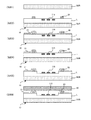
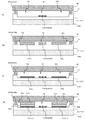
以下、具体的に説明する。図1に示すように、半導体装置100は、積層体10、配線層(最上層配線構造)20、少なくとも2つの熱センサ(感温部)30及び熱センサ(感温部)50、及びヒータ(発熱部)40を有する。図2に示すように、積層体10は、半導体基板SUB、及び配線構造層L1〜L3を含む。なお、配線層20は、積層体10の構成層であり、積層体10に含まれる。図3に示すように、配線構造層L3の上面S10は、保護層21によって被覆されている。保護層21は、壁配線20a、20b間の上面S10には形成されていない。積層体10に保護層21が含まれると把握しても良い。図3に示すように、半導体基板SUBには、MOSトランジスタM100が形成されている。なお、図2は、図1に示すX2−X2に沿う概略的断面模式図であり、図3は、図1に示すX3−X3に沿う部分を含む概略的な断面模式図である。   This will be specifically described below. As shown in FIG. 1, the semiconductor device 100 includes a stacked body 10, a wiring layer (uppermost wiring structure) 20, at least two thermal sensors (temperature sensing parts) 30, a thermal sensor (temperature sensing part) 50, and a heater ( Exothermic part) 40 is included. As illustrated in FIG. 2, the stacked body 10 includes a semiconductor substrate SUB and wiring structure layers L1 to L3. The wiring layer 20 is a constituent layer of the stacked body 10 and is included in the stacked body 10. As shown in FIG. 3, the upper surface S <b> 10 of the wiring structure layer L <b> 3 is covered with the protective layer 21. The protective layer 21 is not formed on the upper surface S10 between the wall wirings 20a and 20b. It may be grasped that the protective layer 21 is included in the laminate 10. As shown in FIG. 3, a MOS transistor M100 is formed in the semiconductor substrate SUB. 2 is a schematic cross-sectional schematic diagram along X2-X2 shown in FIG. 1, and FIG. 3 is a schematic cross-sectional schematic diagram including a portion along X3-X3 shown in FIG.

図1乃至図3に示した半導体装置100は、任意の大きさの半導体IC(Integrated Circuit)チップに設けられており、かつ、不活性ガス(窒素ガス等)が充填されたパッケージ内に気密封止状態で収納されている。パッケージング構成、気密封止方法等は、既存の様々な技術を活用して実現することができる。   The semiconductor device 100 shown in FIGS. 1 to 3 is provided on a semiconductor IC (Integrated Circuit) chip of an arbitrary size and is hermetically sealed in a package filled with an inert gas (nitrogen gas or the like). It is stored in a stopped state. The packaging configuration, hermetic sealing method, and the like can be realized by utilizing various existing technologies.

積層体10は、通常の半導体プロセスによって半導体基板上に複数の層が積層されたものである。積層体10は、半導体基板SUB上に、配線構造層L1〜L3、配線層20、及び保護層21を順に形成することによって形成される。配線構造層L1は、絶縁層に対して配線層を設けたものであり、その余の配線構造層L2、L3についても同様である。なお、図1乃至図3に示す構成は、通常の半導体プロセス(層堆積、フォトリソグラフィー、エッチング、リフトオフ、アニール、スピンコート等)の活用により製造されるものであるが、当業者には自明のため、詳細説明は省略する。   The laminated body 10 is obtained by laminating a plurality of layers on a semiconductor substrate by a normal semiconductor process. The stacked body 10 is formed by sequentially forming the wiring structure layers L1 to L3, the wiring layer 20, and the protective layer 21 on the semiconductor substrate SUB. The wiring structure layer L1 is obtained by providing a wiring layer with respect to the insulating layer, and the same applies to the remaining wiring structure layers L2 and L3. The structure shown in FIGS. 1 to 3 is manufactured by utilizing a normal semiconductor process (layer deposition, photolithography, etching, lift-off, annealing, spin coating, etc.), but is obvious to those skilled in the art. Therefore, detailed description is omitted.

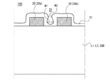
配線層20は、フォトリソグラフィー等によってパターニングされた導電層である。配線層20は、凸状の壁配線20a、および壁配線20bを有する。壁配線20aと壁配線20b間には、ガス流路22が形成されている。壁配線20aは、y軸に沿って延在する長尺な線状配線である。壁配線20bも同様である。ガス流路22も、y軸に沿って延在する。壁配線、及びガス流路は、積層体10の積層方向(z軸方向)に対して直交する軸線に沿って延在する。壁配線は、ヒータやセンサと同じ配線層、若しくはこれらよりも上層の配線層であり、ヒータやセンサを囲うように配置される。これにより、壁配線が配線層構造の上部に形成する凸状の段差が壁となり、その内側にガス流路が形成される。この壁配線は、その表面に酸化膜・ポリイミドなどの絶縁物の皮膜が形成されていてもよく、皮膜がなくとも良い。この場合、特許文献1との比較において、積層体10に対して貫通穴を設ける必要なく、ガス流路を追加の工程なしに設けることができる。また、壁配線を長尺形状とすることによって、同一の半導体基板SUB上に設けられる他の素子の配線空間を十分に確保することができる。換言すれば、同一基板上に設けられる他の素子の配線空間の空きの空間を活用して、一組の壁配線を形成することができるため、チップサイズの大型化は抑制される。   The wiring layer 20 is a conductive layer patterned by photolithography or the like. The wiring layer 20 has convex wall wiring 20a and wall wiring 20b. A gas flow path 22 is formed between the wall wiring 20a and the wall wiring 20b. The wall wiring 20a is a long linear wiring extending along the y-axis. The same applies to the wall wiring 20b. The gas flow path 22 also extends along the y axis. The wall wiring and the gas flow path extend along an axis orthogonal to the stacking direction (z-axis direction) of the stacked body 10. The wall wiring is the same wiring layer as the heater or sensor, or a wiring layer higher than these wiring layers, and is arranged so as to surround the heater or sensor. Thereby, the convex step formed by the wall wiring on the upper part of the wiring layer structure becomes the wall, and the gas flow path is formed inside thereof. This wall wiring may be formed with an insulating film such as an oxide film or polyimide on its surface, or may not have a film. In this case, in comparison with Patent Document 1, it is not necessary to provide a through hole in the stacked body 10, and the gas flow path can be provided without an additional step. In addition, by making the wall wiring into a long shape, a sufficient wiring space for other elements provided on the same semiconductor substrate SUB can be secured. In other words, since a set of wall wirings can be formed by utilizing the space of the wiring space of other elements provided on the same substrate, an increase in chip size is suppressed.

熱センサ30、ヒータ40、および熱センサ50は、露出した態様で、ガス流路22の底面に設けられる。熱センサ30、ヒータ40、および熱センサ50は、配線構造層L3上においてパターニング形成された導電層(好適には、銅(Cu)、アルミニウム(Al)、タングステン(W)、ニッケル(Ni)、チタン(Ti)、クロム(Cr)、鉄(Fe)、金(Au)、白金(Pt)、バナジウム(V)等の金属配線、若しくはそれらの合金、それらの酸化物、窒化物)である。ヒータ40は、熱センサ30、50によって挟まれる。ヒータ40から見て、熱センサ30、50は略等しい位置に配置されている。熱センサ30、50は、ガス流路22に存在するガスを介して、ヒータ40に対して熱接続されている。ヒータ40に対する各熱センサ30、50の間隔を完全に等しいものとする必要はなく、加速度センサのコントローラ側の処理によって、適宜、オフセット調整がされ得るものである。   The heat sensor 30, the heater 40, and the heat sensor 50 are provided on the bottom surface of the gas flow path 22 in an exposed manner. The thermal sensor 30, the heater 40, and the thermal sensor 50 are conductive layers (preferably copper (Cu), aluminum (Al), tungsten (W), nickel (Ni), patterned) formed on the wiring structure layer L3. Metal wiring such as titanium (Ti), chromium (Cr), iron (Fe), gold (Au), platinum (Pt), vanadium (V), or alloys thereof, oxides or nitrides thereof. The heater 40 is sandwiched between the thermal sensors 30 and 50. When viewed from the heater 40, the thermal sensors 30 and 50 are disposed at substantially equal positions. The thermal sensors 30 and 50 are thermally connected to the heater 40 via the gas present in the gas flow path 22. It is not necessary to make the interval between the thermal sensors 30 and 50 with respect to the heater 40 completely equal, and offset adjustment can be appropriately performed by processing on the controller side of the acceleration sensor.

ここで、望ましくは、熱センサ30、ヒータ40、および熱センサ50の表面は極力多くの部分がガスに接することが望ましい。図2をみると、熱センサ30、ヒータ40、および熱センサ50は底面のみが、絶縁物である配線層構造に接しているのみで、側面および上面はガスに接している。この表面積をさらに大きくするために、熱センサ30、ヒータ40、および熱センサ50の表面をエッチングもしくはCVD、もしくはメッキにより凸凹の形状とすると良い。   Here, it is desirable that as many portions of the surfaces of the thermal sensor 30, the heater 40, and the thermal sensor 50 as possible contact the gas. Referring to FIG. 2, only the bottom surfaces of the thermal sensor 30, the heater 40, and the thermal sensor 50 are in contact with the wiring layer structure that is an insulator, and the side surfaces and the top surface are in contact with the gas. In order to further increase the surface area, the surfaces of the thermal sensor 30, the heater 40, and the thermal sensor 50 may be formed into an uneven shape by etching, CVD, or plating.

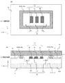
熱センサ30は、上面視矩形状の配線部分(以下、これを単にランドと呼ぶ場合がある)31、上面視矩形状のランド32、およびパターン配線部33を有し、パターニング領域R30に配置される。パターン配線部33は、凸状の配線がy軸に沿って波状に引き回された部分である。パターン配線部は、必ずしも波状でなくとも良い。パターン配線部33を構成する配線の一端は、島状のランド31に対して接続され、その他端は、島状のランド32に対して接続される。パターニング領域R30は、一組の壁配線間に設けられる。   The thermal sensor 30 includes a wiring portion having a rectangular shape when viewed from the top (hereinafter may be simply referred to as a land) 31, a land 32 having a rectangular shape when viewed from the top, and a pattern wiring portion 33, and is disposed in the patterning region R30. The The pattern wiring portion 33 is a portion where the convex wiring is routed in a wave shape along the y-axis. The pattern wiring part does not necessarily have a wave shape. One end of the wiring configuring the pattern wiring portion 33 is connected to the island-shaped land 31, and the other end is connected to the island-shaped land 32. The patterning region R30 is provided between a set of wall wirings.

熱センサ30と同様に、ヒータ40は、ランド41、ランド42、およびパターン配線部43を有し、パターニング領域R40に配置される。熱センサ30と同様に、熱センサ50は、ランド51、ランド52、およびパターン配線部53を有し、パターニング領域R50に配置される。パターン配線部43、53の構成は、パターン配線部33と同様である。パターニング領域R30〜R50は、略等しい面積を有するが、これに限られるべきものではない。ランド31、32、41、42、51、52は、直線状に配置されているが、ランドの配置態様は任意であり、本開示に限定されるべきものではない。パターニング領域R30、R40、R50は、縦幅及び横幅10μM〜30μM程度の大きさの矩形領域である。より高精度な加速度検知を実現するべく、各パターニング領域は、このように微小領域に形成される。   Similar to the thermal sensor 30, the heater 40 includes a land 41, a land 42, and a pattern wiring portion 43, and is disposed in the patterning region R40. Similar to the thermal sensor 30, the thermal sensor 50 includes a land 51, a land 52, and a pattern wiring portion 53, and is disposed in the patterning region R50. The configuration of the pattern wiring parts 43 and 53 is the same as that of the pattern wiring part 33. The patterning regions R30 to R50 have substantially the same area, but should not be limited to this. The lands 31, 32, 41, 42, 51, 52 are arranged in a straight line, but the arrangement form of the lands is arbitrary and should not be limited to the present disclosure. The patterning regions R30, R40, and R50 are rectangular regions having a size of about 10 μM to 30 μM in width and width. In order to realize highly accurate acceleration detection, each patterning region is thus formed in a minute region.

図2に模式的に示すように、配線構造層L3上に設けられた各ランドは、配線構造層L3に設けられたトレンチ配線を介して、配線構造層L2上に設けられた配線層に対して接続される。一例をあげると、ランド31は、トレンチ配線T31を介して、配線層ML31に接続される。なお、トレンチ配線は、絶縁層に対して貫通穴を形成し、この貫通穴に対して導電性材料を充填することによって形成される。   As schematically shown in FIG. 2, each land provided on the wiring structure layer L3 is connected to the wiring layer provided on the wiring structure layer L2 via a trench wiring provided on the wiring structure layer L3. Connected. As an example, the land 31 is connected to the wiring layer ML31 via the trench wiring T31. The trench wiring is formed by forming a through hole in the insulating layer and filling the through hole with a conductive material.

図3に模式的に示すように、半導体基板SUBに形成されたトランジスタM100は、ソース領域(S)、ゲート構造(G)、ドレイン領域(D)を有する。ソース領域は、トレンチ配線Tsを介して、ソース配線層Msに接続される。ゲート電極は、トレンチ配線Tgを介して、ゲート配線層Mgに接続される。ドレイン領域は、トレンチ配線Tdを介して、ドレイン配線層Mdに接続される。ソース配線Msは、不図示の配線接続を介して、他の回路素子に接続される。ゲート配線Mg、ドレイン配線Md、についても同様である。配線構造層L3上には、制御信号入力パッドP1、基準電位供給パッドP2、及び信号出力パッドP3が設けられる。例えば、トランジスタM100が回路素子として含む機能回路は、制御信号入力パッドP1から入力した制御信号に応じて動作する。なお、パッドp1〜p3の配置位置は、通常、チップの周縁部分に配置されるが、ここでは説明の便宜上簡略的な表示している。   As schematically shown in FIG. 3, the transistor M100 formed on the semiconductor substrate SUB has a source region (S), a gate structure (G), and a drain region (D). The source region is connected to the source wiring layer Ms through the trench wiring Ts. The gate electrode is connected to the gate wiring layer Mg via the trench wiring Tg. The drain region is connected to the drain wiring layer Md through the trench wiring Td. The source wiring Ms is connected to other circuit elements via a wiring connection (not shown). The same applies to the gate wiring Mg and the drain wiring Md. A control signal input pad P1, a reference potential supply pad P2, and a signal output pad P3 are provided on the wiring structure layer L3. For example, a functional circuit included in the transistor M100 as a circuit element operates in accordance with a control signal input from the control signal input pad P1. In addition, although the arrangement positions of the pads p1 to p3 are usually arranged at the peripheral portion of the chip, they are simply shown here for convenience of explanation.

図1乃至図3を参酌すれば明らかなように、熱センサ30、ヒータ40、及び熱センサ50を構成する配線パターンは、他の配線構造(例えば、図3に示すパッドP1〜P3)と同層、若しくは、壁配線よりも下層に形成される。これによって、既存の製造プロセスを大幅に変更することなく、熱センサ30、ヒータ40、及び熱センサ50を積層体10に対して組み込むことが可能になる。配線空間の空き空間を活用して上述の配線パターンを形成すれば、既存のチップサイズの拡大を伴うことなく既存のICチップに対して加速度センサを組み込むことができる。   As is clear from FIGS. 1 to 3, the wiring patterns constituting the thermal sensor 30, the heater 40, and the thermal sensor 50 are the same as those of other wiring structures (for example, the pads P1 to P3 shown in FIG. 3). It is formed in a layer or a lower layer than the wall wiring. As a result, the thermal sensor 30, the heater 40, and the thermal sensor 50 can be incorporated into the stacked body 10 without significantly changing the existing manufacturing process. If the above-described wiring pattern is formed by utilizing the free space of the wiring space, the acceleration sensor can be incorporated into the existing IC chip without enlarging the existing chip size.

図4に、ヒータ40の上面視構成を示す。図4に示すように、パターン配線部43に存在する配線の幅は、ヒーターとヒーター駆動回路を結ぶ配線部分の幅よりも狭い。この幅狭配線は、上下に引き回されながら、y軸に沿って波状に延在する。幅狭配線は、通電に応じて発熱する発熱部材であり、上述のように幅狭配線が高密度に敷設されることによって、ガス流路22の底部に微小な熱源が設けられることになる。電源電圧をV、ヒータの抵抗値をRとすると、ヒータの消費電力Pは、P=V/Rであるため、ヒータの抵抗値をある程度確保することがヒータの消費電力の低下につながる。従って、幅狭配線によってヒータの抵抗値を大きくすることで、ヒータの消費電力を低減することが可能になる。なお、ヒータのパターニング構造を単層にて構成する必要はなく、多層(例えば、4層)の配線層を活用してヒータを構成しても良い。これによって、より微小領域にヒータを設けることができ、加速度センサの精度向上を期待できる。 FIG. 4 shows a top view configuration of the heater 40. As shown in FIG. 4, the width of the wiring existing in the pattern wiring portion 43 is narrower than the width of the wiring portion connecting the heater and the heater driving circuit. The narrow wiring extends in a wave shape along the y-axis while being routed up and down. The narrow wiring is a heat generating member that generates heat in response to energization, and the narrow wiring is laid at a high density as described above, whereby a minute heat source is provided at the bottom of the gas flow path 22. If the power supply voltage is V and the heater resistance value is R, the heater power consumption P is P = V 2 / R. Therefore, securing the heater resistance value to some extent leads to a reduction in heater power consumption. Therefore, the power consumption of the heater can be reduced by increasing the resistance value of the heater with the narrow wiring. The heater patterning structure does not need to be configured as a single layer, and the heater may be configured using a multilayer wiring layer (for example, four layers). As a result, a heater can be provided in a finer region, and an improvement in accuracy of the acceleration sensor can be expected.

本実施形態では、パターン配線部43自体は、配線構造層L1〜L3に存在する絶縁層を介して、半導体基板SUBから熱分離されている。ヒータ40のパターン配線部43で生じる熱が半導体基板SUBに対して伝達してしまうと、半導体基板SUBに設けられる素子の動作に影響を与えてしまうおそれがある。本実施形態では、上述のように、パターン配線部43は、配線構造部L1〜L3に存在する絶縁層を介して半導体基板SUB上に形成されているため、半導体基板SUBから見て、パターン配線部43が熱分離された状態となる。パターン配線部43から半導体基板SUBへの熱伝達を抑制することによって、半導体装置100の動作の信頼性を効果的に高めることができる。グランド配線層を活用して、パターン配線部43から半導体基板SUB側への接続配線を介した熱伝達を妨げても良い。   In the present embodiment, the pattern wiring part 43 itself is thermally separated from the semiconductor substrate SUB via the insulating layers present in the wiring structure layers L1 to L3. If the heat generated in the pattern wiring portion 43 of the heater 40 is transferred to the semiconductor substrate SUB, there is a possibility of affecting the operation of elements provided on the semiconductor substrate SUB. In the present embodiment, as described above, the pattern wiring portion 43 is formed on the semiconductor substrate SUB via the insulating layers present in the wiring structure portions L1 to L3. Therefore, the pattern wiring portion 43 is viewed from the semiconductor substrate SUB. The part 43 is in a state of being thermally separated. By suppressing heat transfer from the pattern wiring portion 43 to the semiconductor substrate SUB, the reliability of the operation of the semiconductor device 100 can be effectively increased. The ground wiring layer may be used to prevent heat transfer from the pattern wiring portion 43 to the semiconductor substrate SUB via the connection wiring.

熱センサ30、50は、図4に示したヒータ40と略同様の構成を有する。ただし、熱センサ30、50は、熱を生じさせる必要はないが、周囲の温度変化による抵抗値の変化を検出可能とするために、ヒータ40と同様に幅狭な配線を引き回す構成とする。   The thermal sensors 30 and 50 have substantially the same configuration as the heater 40 shown in FIG. However, although it is not necessary to generate heat, the thermal sensors 30 and 50 have a configuration in which a narrow wiring is routed like the heater 40 in order to detect a change in resistance value due to a change in ambient temperature.

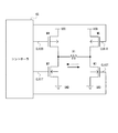
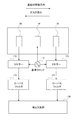
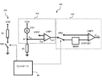
図5を参照してヒータの駆動回路の構成例について説明する。なお、本駆動回路は、図2に示す半導体基板SUB上に設けられるものとする。図5に示すように、ヒータ駆動回路は、電源電位VDDと接地電位GND間に直列接続されたMOSトランジスタM1及び抵抗R1を有する。MOSトランジスタのオン/オフは、コントローラ60によって制御される。図1乃至図3に示したヒータ40は、図5の抵抗R1に相当する。例えば、コントローラ60は、駆動パルスをMOSトランジスタM1のゲート端子に供給する。MOSトランジスタM1は、駆動パルスに応じてオンする。MOSトランジスタM1がオンしている期間、抵抗R1には電流が流れ、ヒータ40は発熱する。   A configuration example of the heater drive circuit will be described with reference to FIG. This drive circuit is provided on the semiconductor substrate SUB shown in FIG. As shown in FIG. 5, the heater drive circuit includes a MOS transistor M1 and a resistor R1 connected in series between the power supply potential VDD and the ground potential GND. On / off of the MOS transistor is controlled by the controller 60. The heater 40 shown in FIGS. 1 to 3 corresponds to the resistor R1 in FIG. For example, the controller 60 supplies a drive pulse to the gate terminal of the MOS transistor M1. The MOS transistor M1 is turned on in response to the drive pulse. While the MOS transistor M1 is on, a current flows through the resistor R1, and the heater 40 generates heat.

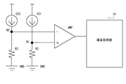
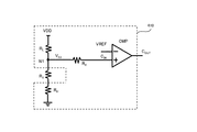
図6を参照して、熱検出回路の構成例について説明する。なお、本熱検出回路は、図2に示す半導体基板SUB上に設けられるものとする。熱検出回路は、熱センサの構成配線の抵抗の温度変化を検出する。シリコン基板上に形成されるメタル配線(銅、アルミニウム等)は、温度1℃について、シート抵抗が1〜2%上昇する。熱検出回路は、この抵抗変化をセンスして、温度を検出する。また、より熱に対する温度変化の大きい酸化バナジウムを使用することも出来る。   A configuration example of the heat detection circuit will be described with reference to FIG. The heat detection circuit is provided on the semiconductor substrate SUB shown in FIG. The heat detection circuit detects a temperature change of the resistance of the constituent wiring of the heat sensor. Metal wiring (copper, aluminum, etc.) formed on a silicon substrate increases sheet resistance by 1 to 2% at a temperature of 1 ° C. The heat detection circuit senses this resistance change and detects the temperature. Further, vanadium oxide having a larger temperature change with respect to heat can also be used.

図6に示すように、熱検出回路は、電流源CS1、抵抗R2、増幅器AMP、演算処理部61を有する。電流源CS1、および抵抗R2は、電源電位VDDと接地電位GND間に直列接続される。増幅器AMPの正入力には、電流源CS1と抵抗R2間の接点が接続される。増幅器AMPの負端子には、参照電圧VREFが接続される。増幅器AMPの出力は、演算処理部61に供給される。図1乃至図3に示した熱センサ30は、図6に示した抵抗R2に相当する。抵抗R2の温度は、ガスを介して伝達するヒータ40の温度に応じて変化する。増幅器AMPの正端子に入力する電圧は、抵抗R2の抵抗値の変化に応じて変動する。増幅器AMPは、参照電圧VREFと入力電圧の差分値を増幅して出力する。なお、図6に示した熱検出回路は、熱センサ50に対しても適用されるものとする。演算処理部61は、各熱センサ30、50に接続された回路から出力される値を演算処理し、加速度を算出する。   As shown in FIG. 6, the heat detection circuit includes a current source CS1, a resistor R2, an amplifier AMP, and an arithmetic processing unit 61. Current source CS1 and resistor R2 are connected in series between power supply potential VDD and ground potential GND. A contact between the current source CS1 and the resistor R2 is connected to the positive input of the amplifier AMP. A reference voltage VREF is connected to the negative terminal of the amplifier AMP. The output of the amplifier AMP is supplied to the arithmetic processing unit 61. The thermal sensor 30 shown in FIGS. 1 to 3 corresponds to the resistor R2 shown in FIG. The temperature of the resistor R2 changes according to the temperature of the heater 40 that is transmitted through the gas. The voltage input to the positive terminal of the amplifier AMP varies according to the change in the resistance value of the resistor R2. The amplifier AMP amplifies and outputs a difference value between the reference voltage VREF and the input voltage. The heat detection circuit shown in FIG. 6 is also applied to the heat sensor 50. The arithmetic processing unit 61 performs arithmetic processing on values output from the circuits connected to the thermal sensors 30 and 50 to calculate acceleration.

図7及び図8を参照して加速度の算出原理/方法について説明する。なお、上述のように、ヒータ40から見て、各熱センサ30、50は略等しい距離をあけて配置されている。従って、半導体装置100が移動してしないとき、各熱センサ30、50は、略同じ熱量を感知する。なお、ヒータに対する熱センサの配置間隔のバラツキの影響を低減するため、熱センサ30、50間に生じるオフセットを調整することが望ましい。これによって、より精度良く加速度を検出することが可能になる。   The acceleration calculation principle / method will be described with reference to FIGS. As described above, when viewed from the heater 40, the thermal sensors 30 and 50 are arranged at substantially equal distances. Accordingly, when the semiconductor device 100 is not moved, the thermal sensors 30 and 50 sense substantially the same amount of heat. Note that it is desirable to adjust the offset generated between the thermal sensors 30 and 50 in order to reduce the influence of the variation in the arrangement interval of the thermal sensors with respect to the heater. This makes it possible to detect the acceleration with higher accuracy.

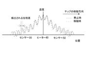
図7に示すように、各熱センサ30、50の温度差に基づいて加速度を算出しても良い。図7に模式的に示すように、半導体装置100が移動すると、半導体装置100から見て、実線で示された熱分布は、点線で示された熱分布へと推移する。熱センサ30の温度は増加し、熱センサ50の温度は減少する。静止時の時刻t1と移動時の時刻t2間では、熱センサ30に温度差が生じる。静止時の時刻t1と移動後の時刻t2間では、熱センサ50に温度差が生じる。各熱センサ30、50が感じる温度差から加速度が算出される。なお、加速度の算出式は、実験的に求められるものであり、その詳細な説明は省略する。   As shown in FIG. 7, the acceleration may be calculated based on the temperature difference between the thermal sensors 30 and 50. As schematically shown in FIG. 7, when the semiconductor device 100 moves, the heat distribution indicated by the solid line transitions to the heat distribution indicated by the dotted line as viewed from the semiconductor device 100. The temperature of the thermal sensor 30 increases and the temperature of the thermal sensor 50 decreases. There is a temperature difference in the thermal sensor 30 between the time t1 when stationary and the time t2 when moving. There is a temperature difference in the thermal sensor 50 between the time t1 at rest and the time t2 after movement. The acceleration is calculated from the temperature difference felt by each of the thermal sensors 30, 50. The acceleration calculation formula is obtained experimentally, and a detailed description thereof is omitted.

ここで、静止時の各熱センサ30、50よりの出力電圧は、センサの位置や、素子ばらつき等で必ずしも一致しない。この場合、加速がかかっていない時の各熱センサの出力を保存しておき、加速がかかっている状態ではこの保存した値との差によって加速を検知する。   Here, the output voltages from the thermal sensors 30 and 50 at rest do not necessarily match due to the position of the sensors, element variations, and the like. In this case, the output of each thermal sensor when acceleration is not applied is stored, and acceleration is detected based on the difference from the stored value when acceleration is applied.

ヒータから熱センサへの熱の伝達経路は、ガスによる経路以外にも層間絶縁膜やシリコン基板を経由するものがある。しかし、ガス以外の経路による熱伝導は本チップに加速がかかっている状態と加速がかかっていない状態で変わらないので、加速がかかっていない時の各熱センサの出力を基準に加速を検知することでこれらの影響を排除できる。   The heat transfer path from the heater to the thermal sensor may be via an interlayer insulating film or a silicon substrate in addition to the gas path. However, the heat conduction through the path other than the gas does not change between when the chip is accelerated and when it is not accelerated, so the acceleration is detected based on the output of each thermal sensor when acceleration is not applied. These effects can be eliminated.

図8に示すように、ヒータ40をパルス駆動させて、各熱センサ30、50の温度変化波形の位相差に基づいて加速度を算出しても良い。図8に模式的に示すように、ヒータ40をパルス駆動すると、ヒータ40を中心として周囲に波状の熱分布が形成される。熱波形の頂部は、オン状態のヒータ40に対応し、熱波形の底部は、オフ状態のヒータ40に対応する。熱センサ30の温度は、時間的に変化する熱波形に応じて変化する。熱センサ50の温度についても同様である。   As shown in FIG. 8, the heater 40 may be pulse-driven and the acceleration may be calculated based on the phase difference between the temperature change waveforms of the thermal sensors 30 and 50. As schematically shown in FIG. 8, when the heater 40 is pulse-driven, a wavy heat distribution is formed around the heater 40. The top of the thermal waveform corresponds to the heater 40 in the on state, and the bottom of the thermal waveform corresponds to the heater 40 in the off state. The temperature of the thermal sensor 30 changes according to the thermal waveform that changes over time. The same applies to the temperature of the thermal sensor 50.

図8に模式的に示すように、半導体装置100が移動すると、半導体装置100から見て、実線で示された熱分布は、点線で示された熱分布へと推移する。これに応じて、熱センサ30の温度変化は、実線に示された熱分布に対応する位相から、点線で示された熱分布に対応する位相へと変化する。図8に模式的に示す熱分布の位相差は、熱センサ30の温度変化の位相変化として検知される。各熱センサ30、50の温度変化の位相差に基づいて、加速度が算出される。なお、加速度の算出式は、実験的に求められるものであり、その詳細な説明は省略する。   As schematically illustrated in FIG. 8, when the semiconductor device 100 moves, the heat distribution indicated by the solid line transitions to the heat distribution indicated by the dotted line as viewed from the semiconductor device 100. In response to this, the temperature change of the thermal sensor 30 changes from the phase corresponding to the heat distribution indicated by the solid line to the phase corresponding to the heat distribution indicated by the dotted line. The phase difference of the heat distribution schematically shown in FIG. 8 is detected as the phase change of the temperature change of the thermal sensor 30. Based on the phase difference of the temperature change of each thermal sensor 30, 50, the acceleration is calculated. The acceleration calculation formula is obtained experimentally, and a detailed description thereof is omitted.

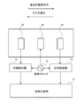
図9を参酌して、図8に示した方式にて加速度を算出する場合の回路構成例について説明する。図9に示すように、基準クロック71は、ヒータ40に対して供給され、位相検出器72、73に個別供給される。ヒータ40は、供給される基準クロック71に応じてパルス駆動される。熱センサ30の温度変化の位相は、基準クロックとの比較に基づいて、位相検出器73により検出される。熱センサ50の温度変化の位相は、基準クロックとの比較に基づいて、位相検出器72により検出される。なお、位相検出器72、73には、図6に示した増幅器AMPの出力が供給されるものとする。位相比較部74は、位相検出器72から供給される波形と位相検出器73から供給される波形間の位相差を検出する。   With reference to FIG. 9, a circuit configuration example in the case of calculating acceleration by the method shown in FIG. 8 will be described. As shown in FIG. 9, the reference clock 71 is supplied to the heater 40 and individually supplied to the phase detectors 72 and 73. The heater 40 is pulse-driven according to the supplied reference clock 71. The phase of the temperature change of the thermal sensor 30 is detected by the phase detector 73 based on the comparison with the reference clock. The phase of the temperature change of the thermal sensor 50 is detected by the phase detector 72 based on the comparison with the reference clock. It is assumed that the phase detectors 72 and 73 are supplied with the output of the amplifier AMP shown in FIG. The phase comparison unit 74 detects a phase difference between the waveform supplied from the phase detector 72 and the waveform supplied from the phase detector 73.

図9に示すように、半導体装置100が移動すると、半導体装置100から見て、ガスは逆方向に流れる。従って、ヒータ40からみて移動方向にある熱センサ30に対してヒータ40からの熱が伝達する時間は、逆側に対する熱センサ50に対してヒータ40から熱が伝達するまでの時間よりも長くなる。図9に示す場合には、この時間差を熱センサの温度変化の位相差として検出し、これに基づいて加速度を算出する。熱センサ30に対する伝達時間(位相検出器73から出力されるパルスの立ち上がりタイミング等から検知する)と熱センサ50に対する伝達時間(位相検出器72から出力されるパルスの立ち上がりタイミング等から検知する)との差分に基づいて加速度を算出することによって、絶対的な温度の検出精度バラツキ等の影響を低減した態様で加速度を算出することができる。図8及び図9に示す方式では、温度の交流的な時間変化検出するため、温度の絶対値は加速度の算出精度に影響を与えない。従って、温度の絶対値を検出する方式に比べて、より精度高く加速度を算出することが可能になる。   As shown in FIG. 9, when the semiconductor device 100 moves, the gas flows in the opposite direction as viewed from the semiconductor device 100. Therefore, the time for which the heat from the heater 40 is transmitted to the heat sensor 30 in the moving direction as viewed from the heater 40 is longer than the time for the heat to be transmitted from the heater 40 to the heat sensor 50 for the opposite side. . In the case shown in FIG. 9, this time difference is detected as the phase difference of the temperature change of the thermal sensor, and the acceleration is calculated based on this. Transmission time to the thermal sensor 30 (detected from the rising timing of the pulse output from the phase detector 73) and transmission time to the thermal sensor 50 (detected from the rising timing of the pulse output from the phase detector 72) By calculating the acceleration based on the difference, the acceleration can be calculated in a manner that reduces the influence of variations in absolute temperature detection accuracy. In the method shown in FIG. 8 and FIG. 9, since an AC time change of temperature is detected, the absolute value of the temperature does not affect the calculation accuracy of the acceleration. Therefore, the acceleration can be calculated with higher accuracy than the method of detecting the absolute value of the temperature.

なお、半導体装置100の具体的な製造手順は任意であり、当業者であれば、適宜、変更等を為すことができる。図1乃至図3に開示した構成は、あくまで例示的なものである。図1乃至図3は、ICチップの部分的な構成を簡略表示したものであり、様々な機能回路/素子が集積されたICチップの全体を表示するものではない。   Note that a specific manufacturing procedure of the semiconductor device 100 is arbitrary, and those skilled in the art can make changes and the like as appropriate. The configurations disclosed in FIGS. 1 to 3 are merely exemplary. FIGS. 1 to 3 simply show a partial configuration of an IC chip, and do not display the entire IC chip on which various functional circuits / elements are integrated.

冒頭で説明したように、本実施形態では、ガス流路22、ヒータ40及び熱センサ30、50を積層体10に設け、ガス流路22の底面にてヒータ40及び熱センサ30、50を露出させる。ガス流路22は、通常の半導体プロセス技術(層堆積、フォトリソグラフィー、エッチング、リフトオフ、基板の貼り合せ、スピンコート、メッキ等)を活用して積層体10に対して設けることができる。ヒータ40及び熱センサ30、50も、同様、通常の半導体プロセス技術を活用して、積層体10に対して設けることができる。これによって、MEMS特有プロセスを経ることなく、通常の半導体プロセスを活用して加速度センサを製造することができる。また、半導体回路チップに対して加速度センサを集積化することも可能になる。   As described at the beginning, in this embodiment, the gas flow path 22, the heater 40 and the thermal sensors 30 and 50 are provided in the laminate 10, and the heater 40 and the thermal sensors 30 and 50 are exposed at the bottom surface of the gas flow path 22. Let The gas flow path 22 can be provided to the stacked body 10 by utilizing a normal semiconductor process technology (layer deposition, photolithography, etching, lift-off, substrate bonding, spin coating, plating, etc.). Similarly, the heater 40 and the thermal sensors 30 and 50 can be provided for the stacked body 10 by utilizing a normal semiconductor process technology. As a result, an acceleration sensor can be manufactured using a normal semiconductor process without going through a MEMS specific process. In addition, the acceleration sensor can be integrated with the semiconductor circuit chip.

半導体回路チップに対する加速度センサの集積化により得られるメリットは、様々なものが考えられる。例えば、半導体回路チップに対する加速度センサの集積化によって、その全体コストを低下させることが可能になると共に、従来必要であった加速度センサのアセンブリの手間を省くことが可能になる。なお、ガス流路、ヒータ、熱センサの具体的構成、個数等は任意である。積層体の具体的な構成についても同様である。   There are various merits that can be obtained by integrating the acceleration sensor with the semiconductor circuit chip. For example, the integration of the acceleration sensor with the semiconductor circuit chip can reduce the overall cost, and can save the time required for the assembly of the acceleration sensor, which has been conventionally required. The specific configuration, number, etc. of the gas flow path, the heater, and the thermal sensor are arbitrary. The same applies to the specific configuration of the laminate.

実施の形態2
図10乃至図12を参照して、実施の形態2について説明する。本実施形態では、実施の形態1とは異なり、熱センサに接続されたPN接合の順方向電圧の変化を検出することによって、熱センサの温度変化、すなわち、熱センサ上に存するガスの温度変化を検出する。抵抗に代えて、PN接合を活用することによって、より精度良く温度変化を検出することが可能になる。なお、PN接合から成るダイオードの順方向電圧は、温度1℃あたり2mV程度変化する。従って、10℃程度の温度変化が生じると、20mV程度の信号を得ることができる。
Embodiment 2
The second embodiment will be described with reference to FIGS. 10 to 12. In this embodiment, unlike Embodiment 1, by detecting a change in the forward voltage of the PN junction connected to the thermal sensor, the temperature change of the thermal sensor, that is, the temperature change of the gas existing on the thermal sensor. Is detected. By using a PN junction instead of a resistor, it becomes possible to detect a temperature change with higher accuracy. Note that the forward voltage of a diode composed of a PN junction changes by about 2 mV per 1 ° C. Therefore, when a temperature change of about 10 ° C. occurs, a signal of about 20 mV can be obtained.

図10は、半導体装置の概略的な断面模式図である。図11は、半導体装置の概略的な上面図である。図12は、熱検出回路を示す回路図である。   FIG. 10 is a schematic cross-sectional schematic view of a semiconductor device. FIG. 11 is a schematic top view of the semiconductor device. FIG. 12 is a circuit diagram showing a heat detection circuit.

図10に示すように、半導体基板SUB(p型基板)には、Nウェル領域11、13が不純物の熱拡散により形成される。Nウェル領域11内には、不純物の熱拡散によりPウェル領域12が形成される。Nウェル領域13内には、Pウェル領域14が形成される。熱センサ30のランド31は、配線構造層に設けられたトレンチ配線T31、T31_2、T31_1、配線ML31、ML31_2を介して、Pウェル領域12に接続される。熱センサ50のランド51は、配線構造層に設けられたトレンチ配線T51、T51_2、T51_1、配線ML51、ML51_2を介して、Pウェル領域14に接続される。   As shown in FIG. 10, N well regions 11 and 13 are formed in a semiconductor substrate SUB (p-type substrate) by thermal diffusion of impurities. A P well region 12 is formed in the N well region 11 by thermal diffusion of impurities. A P well region 14 is formed in the N well region 13. The land 31 of the thermal sensor 30 is connected to the P well region 12 via trench wirings T31, T31_2, T31_1, and wirings ML31, ML31_2 provided in the wiring structure layer. The land 51 of the thermal sensor 50 is connected to the P well region 14 via trench wirings T51, T51_2, T51_1, and wirings ML51, ML51_2 provided in the wiring structure layer.

図11に示すように、Pウェル領域12は、ランド31の直下に形成される。Pウェル領域12の形成範囲は、ランド31の形成範囲よりも広い。Pウェル領域14は、ランド51の直下に形成される。Pウェル領域14の形成範囲は、ランド51の形成範囲よりも広い。なお、Pウェル領域とランド間の相対的な位置関係は任意であり、この例に限られるべきものではない。   As shown in FIG. 11, the P well region 12 is formed immediately below the land 31. The formation range of the P well region 12 is wider than the formation range of the lands 31. The P well region 14 is formed immediately below the land 51. The formation range of the P well region 14 is wider than the formation range of the lands 51. Note that the relative positional relationship between the P well region and the land is arbitrary, and should not be limited to this example.

図12に示す熱検出回路は、図6と比較すると、抵抗R2がダイオードD1に置き換えられている。このようにダイオードD1のカソード電圧の変動に基づいて温度変化を検出することで、より高精度に熱センサの温度を検出することが可能になる。なお、図12において、図11に示す各熱センサ30、50の配線部分は、ダイオードD1のカソード端子と電流源CS1間にある接点N1と電流源CS1間に設けられるものとする。   In the heat detection circuit shown in FIG. 12, the resistor R2 is replaced with a diode D1 as compared with FIG. Thus, by detecting the temperature change based on the fluctuation of the cathode voltage of the diode D1, it becomes possible to detect the temperature of the thermal sensor with higher accuracy. In FIG. 12, the wiring portions of the thermal sensors 30 and 50 shown in FIG. 11 are provided between the contact N1 between the cathode terminal of the diode D1 and the current source CS1 and the current source CS1.

本実施形態においても、パターン配線部43は、配線構造層L1〜L3に存在する絶縁層を介して、半導体基板SUBから熱分離されている。ヒータ40のパターン配線部43で生じる熱が半導体基板SUBに対して伝達してしまうと、半導体基板SUBに設けられるダイオードの動作に影響を与えてしまうおそれがある。本実施形態では、上述のように、パターン配線部43は、配線構造部L1〜L3に存在する絶縁層を介して半導体基板SUB上に形成されているため、半導体基板SUBから見て、パターン配線部43が熱分離された状態となる。パターン配線部43から半導体基板SUBへの熱伝達を抑制することによって、半導体装置100の動作の信頼性を効果的に高めることができる。   Also in the present embodiment, the pattern wiring portion 43 is thermally isolated from the semiconductor substrate SUB via the insulating layers present in the wiring structure layers L1 to L3. If the heat generated in the pattern wiring portion 43 of the heater 40 is transferred to the semiconductor substrate SUB, there is a possibility of affecting the operation of the diode provided on the semiconductor substrate SUB. In the present embodiment, as described above, the pattern wiring portion 43 is formed on the semiconductor substrate SUB via the insulating layers present in the wiring structure portions L1 to L3. Therefore, the pattern wiring portion 43 is viewed from the semiconductor substrate SUB. The part 43 is in a state of being thermally separated. By suppressing heat transfer from the pattern wiring portion 43 to the semiconductor substrate SUB, the reliability of the operation of the semiconductor device 100 can be effectively increased.

実施の形態3
図13及び図14を参照して、実施の形態3について説明する。本実施形態では、熱検出回路は、参照電圧生成回路を含む。このような場合であっても、上述の実施形態と同様の効果を得ることができる。
Embodiment 3
The third embodiment will be described with reference to FIGS. 13 and 14. In the present embodiment, the heat detection circuit includes a reference voltage generation circuit. Even in such a case, the same effect as that of the above-described embodiment can be obtained.

図13は、熱検出回路を示す回路図である。図14は、熱検出回路の動作原理を示す図である。   FIG. 13 is a circuit diagram showing a heat detection circuit. FIG. 14 is a diagram illustrating the operation principle of the heat detection circuit.

図13に示すように、電流源CS3と抵抗R3間の接点が増幅器(比較器)AMPの負端子に接続される。抵抗R3の熱容量は、抵抗R2と比較して大幅に大きい。抵抗R3は、抵抗R2に対して近接配置され、同タイミングに略同じ温度となる。図14の実線は、ヒータ40の間欠的駆動に応じた抵抗R2の温度変化を示す。図14の破線は、ヒータ40の間欠的駆動に応じて抵抗R3の温度変化を示す。図14から明らかなように、熱容量が大きな抵抗R3は、ガスを介して伝わる熱の影響をあまり受けない。増幅器AMPの負端子に入力する電圧は、略一定なものとなる。抵抗R2、R3の抵抗値の大小は、温度変化に追従して入れ替わるため、増幅器AMPは、温度変動の位相を検出することができる。これによって、比較的単純な構成で熱検出回路を形成することができる。抵抗R2と抵抗R3の相違点は、主として、ガス流路22内での露出面積であり、製造プロセス的に考慮しても大きな負担とはならない。   As shown in FIG. 13, the contact between the current source CS3 and the resistor R3 is connected to the negative terminal of the amplifier (comparator) AMP. The heat capacity of the resistor R3 is significantly larger than that of the resistor R2. The resistor R3 is disposed close to the resistor R2, and has substantially the same temperature at the same timing. The solid line in FIG. 14 shows the temperature change of the resistor R2 according to the intermittent driving of the heater 40. The broken line in FIG. 14 shows the temperature change of the resistor R3 according to the intermittent driving of the heater 40. As is apparent from FIG. 14, the resistor R3 having a large heat capacity is not significantly affected by the heat transmitted through the gas. The voltage input to the negative terminal of the amplifier AMP is substantially constant. Since the resistance values of the resistors R2 and R3 are switched following the temperature change, the amplifier AMP can detect the phase of the temperature fluctuation. As a result, the heat detection circuit can be formed with a relatively simple configuration. The difference between the resistor R2 and the resistor R3 is mainly the exposed area in the gas flow path 22, and it does not become a big burden even if it is considered in the manufacturing process.

実施の形態4
図15及び図16を参照して、実施の形態4について説明する。本実施形態では、抵抗R1、つまり、ヒータ40は、時分割して順方向及び逆方向に通電される。上述の実施形態において説明したように、ヒータ40は、通電発熱する幅狭配線を有するため、通電方向を固定した場合には、エレクトロマイグレーションによって幅狭配線が劣化してしまうおそれがある。本実施形態では、この点に考慮し、ヒータ40の通電方向を適当な間隔で逆方向として、ヒータ40の構成配線の劣化を抑制する。これによって、ヒータ40の寿命を延ばし、より信頼性高い加速度センサを提供することが可能になる。
Embodiment 4
The fourth embodiment will be described with reference to FIGS. 15 and 16. In the present embodiment, the resistor R1, that is, the heater 40 is energized in the forward direction and the reverse direction in a time-sharing manner. As described in the above-described embodiment, the heater 40 has a narrow wiring that generates electricity and generates heat. Therefore, when the energization direction is fixed, the narrow wiring may be deteriorated by electromigration. In this embodiment, considering this point, the energization direction of the heater 40 is reversed at an appropriate interval to suppress deterioration of the constituent wiring of the heater 40. Accordingly, it is possible to extend the life of the heater 40 and provide a more reliable acceleration sensor.

図15は、ヒータの駆動回路を示す回路図である。図16は、ヒータの駆動回路の動作を示すタイミングチャートである。   FIG. 15 is a circuit diagram showing a heater drive circuit. FIG. 16 is a timing chart showing the operation of the heater drive circuit.

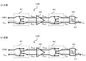
図15に示すように、ヒータ40の駆動回路は、MOSトランジスタM2〜M5、抵抗R1、コントローラ65を有する。MOSトランジスタM2、M4は、電源電位VDDと接地電位GND間に直列接続される。MOSトランジスタM3、M5は、電源電位VDDと接地電位GND間に直列接続される。抵抗R1は、MOSトランジスタM2とMOSトランジスタM4間の接点とMOSトランジスタM3とMOSトランジスタM5間の接点との間に設けられる。各MOSトランジスタのオン/オフは、コントローラ65によって図16に示すように制御される。   As shown in FIG. 15, the drive circuit of the heater 40 includes MOS transistors M2 to M5, a resistor R1, and a controller 65. MOS transistors M2 and M4 are connected in series between power supply potential VDD and ground potential GND. MOS transistors M3 and M5 are connected in series between power supply potential VDD and ground potential GND. The resistor R1 is provided between the contact between the MOS transistor M2 and the MOS transistor M4 and the contact between the MOS transistor M3 and the MOS transistor M5. On / off of each MOS transistor is controlled by the controller 65 as shown in FIG.

図16に示すように、時刻t1と時刻t2の期間、トランジスタM3、M4がオンし、トランジスタM2、M5がオフする。図15を正面視して、抵抗R1には、左から右方向へ(順方向へ)電流が流れる。時刻t2と時刻t3の期間、トランジスタM2〜M5がオンし、抵抗R1には電流が流れない。時刻t3と時刻t4の期間、トランジスタM3、M4がオフし、トランジスタM2、M5がオンする。図15を正面視して、抵抗R1には、右から左方向へ(逆方向へ)電流が流れる。時刻t4と時刻t5の期間、トランジスタM2〜M5がオンし、抵抗R1には電流が流れない。このようなサイクルを繰り返すことによって、抵抗R1、すなわちヒータ40には時分割して順方向/逆方向に電流が流れ、ヒータ40の経年劣化を抑制することができる。   As shown in FIG. 16, during the period between time t1 and time t2, the transistors M3 and M4 are turned on and the transistors M2 and M5 are turned off. When FIG. 15 is viewed from the front, a current flows through the resistor R1 from the left to the right (forward). During the period between time t2 and time t3, the transistors M2 to M5 are turned on, and no current flows through the resistor R1. During the period between time t3 and time t4, the transistors M3 and M4 are turned off and the transistors M2 and M5 are turned on. When FIG. 15 is viewed from the front, a current flows from the right to the left (in the reverse direction) through the resistor R1. During the period between time t4 and time t5, the transistors M2 to M5 are turned on, and no current flows through the resistor R1. By repeating such a cycle, current flows through the resistor R1, that is, the heater 40 in a time-sharing manner in the forward / reverse direction, and the aging of the heater 40 can be suppressed.

実施の形態5
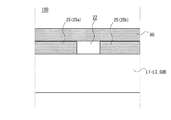
図17を参照して、実施の形態5について説明する。本実施形態では、上述の実施形態の構成に加えて、図17に示すように、保護層21上にカバー板(カバー部材)80を配置し、ガス流路22を上方から被覆する。これによって、ガス流路22の上方が閉じた状態となり、ヒータ40からガス流路22内のガスに伝達した熱が上方へ拡散してしまうことを効果的に抑制することができる。好適には、熱導電性が半導体よりも低いガラス板、セラミック板をカバー板80として採用すると良い。ガス流路22を覆うカバー部材は、カバー板80のような平板状部材に限られるべきものではない。
Embodiment 5
The fifth embodiment will be described with reference to FIG. In this embodiment, in addition to the configuration of the above-described embodiment, as shown in FIG. 17, a cover plate (cover member) 80 is disposed on the protective layer 21, and the gas flow path 22 is covered from above. Thereby, the upper part of the gas flow path 22 is closed, and it is possible to effectively suppress the heat transmitted from the heater 40 to the gas in the gas flow path 22 from diffusing upward. Preferably, a glass plate or a ceramic plate whose thermal conductivity is lower than that of a semiconductor is used as the cover plate 80. The cover member that covers the gas flow path 22 should not be limited to a flat plate member such as the cover plate 80.

実施の形態6
図18を参照して、実施の形態6について説明する。本実施形態では、上述の実施形態の構成に加えて、図18に示すように、壁配線20aと壁配線20b間に存在する保護層21によってガス流路22を形成する。壁配線間へ保護層が侵入できないと、壁配線間には図18に示すように、ガス流路として機能する空洞が形成される。図18に示すように、ガス流路22の幅は、半導体基板SUBから離間する方向に沿って幅狭くなる(W1>W2)。これによって、ガス流路22の上方を絞った状態とすることができ、ヒータ40により加熱されたガスが上方へ逃げることを抑制することができる。ガス流路22内にヒータ40により加熱されたガスを閉じ込めることによって、熱センサ30、50によるガス温度の検出精度を高めることができる。
Embodiment 6
Embodiment 6 will be described with reference to FIG. In the present embodiment, in addition to the configuration of the above-described embodiment, as shown in FIG. 18, the gas flow path 22 is formed by the protective layer 21 existing between the wall wiring 20a and the wall wiring 20b. If the protective layer cannot penetrate between the wall wirings, a cavity functioning as a gas flow path is formed between the wall wirings as shown in FIG. As shown in FIG. 18, the width of the gas flow path 22 becomes narrower along the direction away from the semiconductor substrate SUB (W1> W2). Thus, the upper portion of the gas flow path 22 can be narrowed, and the gas heated by the heater 40 can be prevented from escaping upward. By confining the gas heated by the heater 40 in the gas flow path 22, the detection accuracy of the gas temperature by the thermal sensors 30 and 50 can be increased.

実施の形態7
図19を参照して、実施の形態7について説明する。本実施形態では、上述の実施形態とは異なり、配線層20のパターニングによりガス流路22を形成するのではなく、長尺な開口が設けられた板状部材を基板上(配線構造層上)に配置することによってガス流路22を形成する。このような場合であって、上述の実施形態と同様の効果を得ることができる。
Embodiment 7
The seventh embodiment will be described with reference to FIG. In the present embodiment, unlike the above-described embodiment, the gas flow path 22 is not formed by patterning the wiring layer 20, but a plate-like member provided with a long opening is provided on the substrate (on the wiring structure layer). The gas flow path 22 is formed by arrange | positioning. In such a case, the same effect as that of the above-described embodiment can be obtained.

図19に示すように、基板(半導体基板SUB、配線構造層L1〜L3)上には、板状部材(最上層配線構造)25が配置される。板状部材25は、例えば、ガラス板、セラミック板等である。板状部材25には、開口が設けられており、これがガス流路22として機能する。なお、図19では、説明の便宜上、ヒータ、熱センサ等の図示は省略されている。基板上に板状部材を積層する具体的な方法は任意である。例えば、基板に対して板状部材を貼り合わせることによって、基板上に板状部材を積層すると良い。基板に対する板状部材の固定方法は任意である。例えば、板状部材は、接着剤を介して、基板上に固定される。この場合、接着剤は、ガス流路22には侵入しない範囲で塗布される。   As shown in FIG. 19, a plate-like member (uppermost layer wiring structure) 25 is disposed on a substrate (semiconductor substrate SUB, wiring structure layers L1 to L3). The plate-like member 25 is, for example, a glass plate or a ceramic plate. The plate-like member 25 is provided with an opening, which functions as the gas flow path 22. In FIG. 19, for convenience of explanation, illustration of a heater, a heat sensor, and the like is omitted. A specific method for laminating the plate-like member on the substrate is arbitrary. For example, the plate member may be stacked on the substrate by bonding the plate member to the substrate. The method for fixing the plate-like member to the substrate is arbitrary. For example, the plate-like member is fixed on the substrate via an adhesive. In this case, the adhesive is applied in a range that does not enter the gas flow path 22.

実施の形態8
図20を参照して、実施の形態8について説明する。本実施形態では、図19に対して図17に開示のカバー板80を適用する。このような場合であっても、上述の実施形態と同様の効果を得ることができる。
Embodiment 8
The eighth embodiment will be described with reference to FIG. In the present embodiment, the cover plate 80 disclosed in FIG. 17 is applied to FIG. Even in such a case, the same effect as that of the above-described embodiment can be obtained.

実施の形態9
図21を参照して、実施の形態9について説明する。本実施形態では、図4とは異なる態様にて配線を施してヒータを構成する。このような場合であっても、上述の実施形態と同様の効果を得ることができる。図21に示すように、ヒータは、渦巻き状に巻かれた配線から構成される。配線の一端は、トレンチを介して、配線構造層内の配線に接続される。配線の他端についても同様である。図21に示すヒータは、一辺が9.6μM程度の大きさの矩形領域に設けられる。熱センサの配線引き回し態様についても、図21と同様としても良い。
Embodiment 9
A ninth embodiment will be described with reference to FIG. In the present embodiment, the heater is configured by wiring in a manner different from that in FIG. Even in such a case, the same effect as that of the above-described embodiment can be obtained. As shown in FIG. 21, the heater is composed of wiring wound in a spiral shape. One end of the wiring is connected to the wiring in the wiring structure layer through the trench. The same applies to the other end of the wiring. The heater shown in FIG. 21 is provided in a rectangular region having a side of about 9.6 μM. The wiring pattern of the thermal sensor may be the same as in FIG.

実施の形態10
図22を参照して、実施の形態10について説明する。本実施形態では、熱検出回路及びヒータ駆動回路は、ヒータ40の発熱による特性変動を回避するために、熱センサ30、ヒータ40、熱センサ50から離れた位置に設ける。より好適には、図22に模式的に示した配置間隔から読み取れるように、ヒータ40と熱センサ30との間隔(例えば、間隔W90)よりも、ヒータ40とヒータ駆動回路間の間隔(例えば、間隔W91)のほうが広い。同様に、ヒータ40と熱センサ30との間隔よりも、熱センサ30と熱検出回路間の間隔(例えば、間隔W92)のほうが広い。これによって、好適に、ヒータ40で生じる熱影響によって、各回路特性が変動してしまうことを抑制することが可能になる。なお、その余の点は、上述の実施形態と同様であり、重複説明は省略する。本実施形態においても上述の実施形態で説明したものと同様の効果を得ることができる。
Embodiment 10
Embodiment 10 will be described with reference to FIG. In the present embodiment, the heat detection circuit and the heater drive circuit are provided at positions away from the heat sensor 30, the heater 40, and the heat sensor 50 in order to avoid characteristic fluctuation due to heat generation of the heater 40. More preferably, as can be read from the arrangement interval schematically shown in FIG. 22, the interval between the heater 40 and the heater drive circuit (for example, the interval W90) is larger than the interval between the heater 40 and the thermal sensor 30 (for example, the interval W90). The interval W91) is wider. Similarly, the interval between the heat sensor 30 and the heat detection circuit (for example, the interval W92) is wider than the interval between the heater 40 and the heat sensor 30. Accordingly, it is possible to suppress the fluctuation of each circuit characteristic due to the thermal effect generated by the heater 40. The remaining points are the same as in the above-described embodiment, and a duplicate description is omitted. Also in this embodiment, the same effects as those described in the above embodiment can be obtained.

実施の形態11
図23を参照して、実施の形態11について説明する。本実施形態では、図23に示す検出構成を採用する。図23に示すように、熱センサ50の出力とヒータ40のクロック信号をミキシングし、ミキサー172の出力信号からローパスフィルタ174を介して低周波成分を選択通過させる。また、熱センサ30の出力とヒータ40のクロック信号をミキシングし、ミキサー173の出力信号からローパスフィルタ175を介して低周波成分を選択通過させる。電圧比較部176は、ローパスフィルタ174、175からの各入力電圧値を比較する。
Embodiment 11
The eleventh embodiment will be described with reference to FIG. In this embodiment, the detection configuration shown in FIG. 23 is adopted. As shown in FIG. 23, the output of the thermal sensor 50 and the clock signal of the heater 40 are mixed, and the low-frequency component is selectively passed through the low-pass filter 174 from the output signal of the mixer 172. Further, the output of the thermal sensor 30 and the clock signal of the heater 40 are mixed, and the low frequency component is selectively passed through the low pass filter 175 from the output signal of the mixer 173. The voltage comparison unit 176 compares the input voltage values from the low pass filters 174 and 175.

熱センサ30、50の出力信号は、半導体装置100に加速がかかっていない状態では、ヒータ40のクロック信号にほぼ一致するが、半導体装置100に加速がかかっている状態では、ガスによる熱伝導分だけクロック信号が変調される。熱センサ30、50から出力される変調信号を、クロック信号とミキシングすると、クロック信号の2倍の周波成分を持つ信号とDC近辺の低周波信号とが合成された信号となる。ローパスフィルタによって低域通過させるとDC近辺の信号を抽出することができる。ローパスフィルタの出力電圧値は、ガスによる熱伝導による変調分だけ変化する。この原理に基づいて、電圧比較部176は、各ローパスフィルタ174、175の出力電圧値を比較する。電圧比較部176による比較結果に基づいて加速度を検知することが可能になる。なお、その余の点は、上述の実施形態と同様であり、重複説明は省略する。本実施形態においても上述の実施形態で説明したものと同様の効果を得ることができる。   The output signals of the thermal sensors 30 and 50 substantially coincide with the clock signal of the heater 40 when the semiconductor device 100 is not accelerated. However, when the semiconductor device 100 is accelerated, the heat conduction component due to the gas. Only the clock signal is modulated. When the modulation signals output from the thermal sensors 30 and 50 are mixed with a clock signal, a signal having a frequency component twice that of the clock signal and a low-frequency signal near DC are combined. When a low-pass filter is used to pass a low band, a signal in the vicinity of DC can be extracted. The output voltage value of the low-pass filter changes by the amount of modulation due to heat conduction by gas. Based on this principle, the voltage comparison unit 176 compares the output voltage values of the low-pass filters 174 and 175. The acceleration can be detected based on the comparison result by the voltage comparison unit 176. The remaining points are the same as in the above-described embodiment, and a duplicate description is omitted. Also in this embodiment, the same effects as those described in the above embodiment can be obtained.

実施の形態12
図24及び図25を参照して、実施の形態12について説明する。本実施形態では、図24に示すように、N領域13とP領域14間の接合位置を熱センサ30から離れた位置とする。同様に、N領域11とP領域12間の接合位置を熱センサ50から離れた位置とする。このようにダイオード間の距離を確保することによって、半導体基板SUBを介したダイオード間の熱伝導の影響を低減することができる。なお、W200<W201<W202<W204の関係が成立している。
Embodiment 12
The twelfth embodiment will be described with reference to FIGS. 24 and 25. FIG. In the present embodiment, as shown in FIG. 24, the joining position between the N region 13 and the P region 14 is a position away from the thermal sensor 30. Similarly, the joining position between the N region 11 and the P region 12 is a position away from the thermal sensor 50. By ensuring the distance between the diodes in this way, it is possible to reduce the influence of heat conduction between the diodes via the semiconductor substrate SUB. Note that the relationship of W200 <W201 <W202 <W204 is established.

図25に示すように、ヒータ40と半導体基板SUB間、端的にはヒータ40の直下に放熱用の配線ML200を配置すると良い。これによって、ヒータ40から半導体基板SUBを介してダイオードに伝わる熱伝導の経路を遮断することができ、ガス経由で伝わる熱による熱センサの感度を高めることができる。好適には、配線ML200は、グランド若しくは一定電位に固定することが望ましい。配線ML200の電位固定用の引き出し配線は、熱伝導の経路となるため、ヒータ駆動用配線に近付けて配置することが望ましく、この引き出し配線をグランド又は一定電位に接続する接続点はヒータ駆動回路近辺に配置することが望ましい。その余の点は、上述の実施形態と同様であり、重複説明は省略する。本実施形態においても上述の実施形態で説明したものと同様の効果を得ることができる。   As shown in FIG. 25, it is preferable to dispose a heat radiation wiring ML200 between the heater 40 and the semiconductor substrate SUB, that is, directly below the heater 40. As a result, the heat conduction path transmitted from the heater 40 to the diode via the semiconductor substrate SUB can be cut off, and the sensitivity of the heat sensor due to the heat transmitted via the gas can be increased. The wiring ML200 is preferably fixed to the ground or a constant potential. Since the lead wire for fixing the potential of the wire ML200 serves as a heat conduction path, it is desirable to place it close to the heater drive wire. The connection point for connecting the lead wire to the ground or a constant potential is near the heater drive circuit. It is desirable to arrange in. The other points are the same as those in the above-described embodiment, and a duplicate description is omitted. Also in this embodiment, the same effects as those described in the above embodiment can be obtained.

実施の形態13
図26を参照して、実施の形態13について説明する。本実施形態では、図26に示すように、ヒータ40の周囲に4つの熱センサ30(50)を配置する。4つの熱センサ30は、ヒータ40を中心として、ある熱センサを90度ずつ回転させた位置に配置されている。
Embodiment 13
A thirteenth embodiment will be described with reference to FIG. In this embodiment, as shown in FIG. 26, four thermal sensors 30 (50) are arranged around the heater 40. The four thermal sensors 30 are arranged at positions where a certain thermal sensor is rotated 90 degrees around the heater 40.

換言すると、次のように説明できる。熱センサ30aと熱センサ30cは、ヒータ40を中心に挟んで対称配置されている。熱センサ30bと熱センサ30dは、ヒータ40を中心に挟んで対称配置されている。熱センサ30aと熱センサ30cの組の配置方向は、熱センサ30bと熱センサ30dの配置方向に対して略直交する。   In other words, it can be explained as follows. The heat sensor 30a and the heat sensor 30c are arranged symmetrically with the heater 40 as the center. The thermal sensor 30b and the thermal sensor 30d are arranged symmetrically with the heater 40 as the center. The arrangement direction of the set of the thermal sensor 30a and the thermal sensor 30c is substantially orthogonal to the arrangement direction of the thermal sensor 30b and the thermal sensor 30d.

この構成を採用することによって、熱センサ30aと熱センサ30cの組の出力の比較によってx軸方向の加速度を検出し、熱センサ30bと熱センサ30dの組の出力の比較によってy軸方向の加速度を検出することが可能となる。これにより、よりコンパクトな構成にて複数方向の変位を検出することが可能となる。なお、その余の点は、上述の実施形態と同様であり、重複説明は省略する。本実施形態においても上述の実施形態で説明したものと同様の効果を得ることができる。   By adopting this configuration, the acceleration in the x-axis direction is detected by comparing the output of the set of the thermal sensor 30a and the thermal sensor 30c, and the acceleration in the y-axis direction is detected by comparing the output of the set of the thermal sensor 30b and the thermal sensor 30d. Can be detected. Thereby, it becomes possible to detect displacement in a plurality of directions with a more compact configuration. The remaining points are the same as in the above-described embodiment, and a duplicate description is omitted. Also in this embodiment, the same effects as those described in the above embodiment can be obtained.

なお、本発明は上記実施の形態に限られたものではなく、趣旨を逸脱しない範囲で適宜変更することが可能である。最上層配線構造の具体的な材質は任意であり、絶縁層により構成しても良い。ヒータ、熱センサ等の構成配線をポリシリコン等により構成しても良い。ガス流路の延在態様は、任意であり、直線状に限られない。   Note that the present invention is not limited to the above-described embodiment, and can be changed as appropriate without departing from the spirit of the present invention. The specific material of the uppermost layer wiring structure is arbitrary and may be constituted by an insulating layer. Constituent wiring such as a heater and a heat sensor may be made of polysilicon or the like. The extending aspect of the gas flow path is arbitrary and is not limited to a straight line.

実施の形態14
ここで、本発明と従来技術との相違を明確にするために、本発明適用前の参考例について説明する。図27(a)及び(b)は、特許文献1に記載された熱型加速度センサを封止形成した参考例の上面断面図及び側面断面図である。
Embodiment 14
Here, in order to clarify the difference between the present invention and the prior art, a reference example before application of the present invention will be described. 27A and 27B are a top sectional view and a side sectional view of a reference example in which the thermal acceleration sensor described in Patent Document 1 is sealed.

参考例の加速度センサ900では、シリコン基板901の内部に、ガスを封入するチャンバー(空洞部)902が掘りこまれて形成されている。チャンバー902の上面視中央かつ側面視中央には、ヒータ903が配置されている。ヒータ903は、加速度センサ900の一方の側面から対向する他方の側面まで延在配置されている。ヒータ903の両側には、熱センサ904、905が配置されている。熱センサ904,905は、ヒータ903と平行に加速度センサ900の一方の側面から対向する他方の側面まで延在配置されている。すなわち、参考例の加速度センサ900では、シリコン基板901を削り取って形成しているため、内部のチャンバー902は、シリコン基板901の外形と同様、上面断面及び側面断面が長方形状である。また、ヒータ903、熱センサ904、905は、チャンバー902の中空に浮いた状態で形成されている。   In the acceleration sensor 900 of the reference example, a chamber (hollow part) 902 that encloses a gas is dug inside the silicon substrate 901. A heater 903 is disposed in the center of the chamber 902 in the top view and the side view. The heater 903 extends from one side surface of the acceleration sensor 900 to the other side surface facing the heater 903. Thermal sensors 904 and 905 are disposed on both sides of the heater 903. The thermal sensors 904 and 905 are arranged in parallel with the heater 903 so as to extend from one side surface of the acceleration sensor 900 to the opposite side surface. That is, in the acceleration sensor 900 of the reference example, since the silicon substrate 901 is cut and formed, the inner chamber 902 has a rectangular top surface and side surface cross section, similar to the outer shape of the silicon substrate 901. The heater 903 and the thermal sensors 904 and 905 are formed in a state of floating in the hollow of the chamber 902.

参考例の加速度センサ900では、ヒータ903によりチャンバー902内のガスが加熱され、ガスの温度を熱センサ904、905が検出する。参考例の加速度センサ900が移動するとチャンバー902内のガスは、加速度センサ900の動きに追従できないため、加速度センサ900の移動方向とは逆に流れる。そうすると、ガスの温度分布が、ヒータ903の両側の熱センサ904の位置と熱センサ905の位置とで非対称となる。そこで、参考例の加速度センサ900では、熱センサ903、904の出力を比較することで、加速度センサ900に印加される加速度を検出している。   In the acceleration sensor 900 of the reference example, the gas in the chamber 902 is heated by the heater 903, and the temperature of the gas is detected by the thermal sensors 904 and 905. When the acceleration sensor 900 of the reference example moves, the gas in the chamber 902 cannot follow the movement of the acceleration sensor 900 and flows in the direction opposite to the movement direction of the acceleration sensor 900. Then, the temperature distribution of the gas becomes asymmetric between the position of the thermal sensor 904 on both sides of the heater 903 and the position of the thermal sensor 905. Therefore, in the acceleration sensor 900 of the reference example, the acceleration applied to the acceleration sensor 900 is detected by comparing the outputs of the thermal sensors 903 and 904.

次に、図28を用いて、本実施形態に係る半導体装置100について説明する。図28(a)及び(b)は、本実施形態に係る半導体装置100の上面断面図及び側面断面図である。   Next, the semiconductor device 100 according to the present embodiment will be described with reference to FIG. 28A and 28B are a top sectional view and a side sectional view of the semiconductor device 100 according to the present embodiment.

図1では、半導体装置100の一部を記載していたため、Y方向に延びる壁配線20a、20bのみが記載されていたが、図28では、ガスを封入する空洞部を形成するための壁配線の全体が記載されている。   Since only a part of the semiconductor device 100 is described in FIG. 1, only the wall wirings 20 a and 20 b extending in the Y direction are illustrated. However, in FIG. 28, the wall wiring for forming a cavity that encloses gas is illustrated. The whole is described.

図28に示すように、半導体装置100は、積層体10、最上層配線構造20(壁配線20a、20b)、熱センサ30、熱センサ50、及びヒータ40を有する。なお、壁配線は連続した配線として形成されるため、以下では、壁配線全体を20aもしくは20bと称する。   As shown in FIG. 28, the semiconductor device 100 includes a stacked body 10, an uppermost layer wiring structure 20 (wall wirings 20 a and 20 b), a thermal sensor 30, a thermal sensor 50, and a heater 40. Since the wall wiring is formed as a continuous wiring, the entire wall wiring is hereinafter referred to as 20a or 20b.

積層体10は、シリコン基板である半導体基板SUB、及び配線構造層Lを含む。配線構造層Lは、図2等と同様に、配線構造層L1〜L3を含み、各配線構造層は層間絶縁膜及び配線層を含んでいる。また、最上層配線構造20は、最上層に形成されたメタル配線(配線層)であり、壁配線20aを構成している。   The stacked body 10 includes a semiconductor substrate SUB, which is a silicon substrate, and a wiring structure layer L. Similar to FIG. 2 and the like, the wiring structure layer L includes wiring structure layers L1 to L3, and each wiring structure layer includes an interlayer insulating film and a wiring layer. The uppermost layer wiring structure 20 is a metal wiring (wiring layer) formed in the uppermost layer and constitutes a wall wiring 20a.

この例では、壁配線20a、ヒータ40及び熱センサ30、50は、同じ最上層に形成されている。積層体10の最上層に、ヒータ40を配置し、そのY方向両側に熱センサ30、50を配置する。なお、ヒータ40、熱センサ30及び50の各配線あるいは全ての配線をヒータ・熱センサ配線110とも称する。   In this example, the wall wiring 20a, the heater 40, and the thermal sensors 30, 50 are formed in the same uppermost layer. The heater 40 is disposed on the uppermost layer of the laminated body 10, and the thermal sensors 30 and 50 are disposed on both sides in the Y direction. In addition, each wiring or all wiring of the heater 40 and the thermal sensors 30 and 50 is also referred to as a heater / thermal sensor wiring 110.

上面視で、ヒータ・熱センサ配線110の周囲を略長方形状に囲うように、ガス流を制限する壁配線20a(20b)が配置される。配線構造層Lの上面S10及び壁配線20aは、保護層(カバー膜)21によって被覆されている。保護層21は、壁配線20aの内側の上面S10には形成されていない。すなわち、ヒータ・熱センサ配線110は、保護層21に覆われていない状態であり、配線の表面がガスに露出している。   Wall wiring 20a (20b) for restricting the gas flow is arranged so as to surround the heater / thermal sensor wiring 110 in a substantially rectangular shape when viewed from above. The upper surface S10 and the wall wiring 20a of the wiring structure layer L are covered with a protective layer (cover film) 21. The protective layer 21 is not formed on the upper surface S10 inside the wall wiring 20a. That is, the heater / thermal sensor wiring 110 is not covered with the protective layer 21, and the surface of the wiring is exposed to gas.

また、図17と同様に、突出した保護層21上にカバー板80が配置される。カバー板80は、ガラス基板やシリコン基板等である。壁配線20aの上面全体に、保護層21を介してカバー板80が張り付けられている。   Similarly to FIG. 17, the cover plate 80 is disposed on the protruding protective layer 21. The cover plate 80 is a glass substrate, a silicon substrate, or the like. A cover plate 80 is attached to the entire upper surface of the wall wiring 20a via a protective layer 21.

壁配線20aがカバー板80と接触すると、壁配線20aで囲まれた領域は閉鎖された空洞部24となる。すなわち、空洞部24は、上面側をカバー板80に覆われ、底面側を最上層に接する配線構造層L(L3)の層間絶縁膜に覆われ、側面側を壁配線20aに覆われて封止形成されている。空洞部24の空間のうち、ヒータ・熱センサ配線110近傍の領域をガス流路22、ガス流路22のY方向(ガスの流れる方向)両側の領域をキャビティ23(23a、23b)と称する。この空洞部24に、大気、窒素、もしくはアルゴンなどのガスが封入されている。   When the wall wiring 20 a comes into contact with the cover plate 80, the region surrounded by the wall wiring 20 a becomes a closed cavity 24. That is, the cavity 24 is covered with the cover plate 80 on the upper surface side, covered with the interlayer insulating film of the wiring structure layer L (L3) in contact with the uppermost layer, and covered with the wall wiring 20a on the side surface side. It is stopped. Of the space of the cavity 24, a region in the vicinity of the heater / thermal sensor wiring 110 is referred to as a gas flow path 22, and regions on both sides in the Y direction (gas flow direction) of the gas flow path 22 are referred to as cavities 23 (23 a, 23 b). The cavity 24 is filled with a gas such as air, nitrogen, or argon.

図28のような構造の半導体装置100において、図7や図8で示したように、ヒータ40で空洞部24内のガスを加熱し、ガスの温度分布を熱センサ30、50で測定し、熱センサ30,50の温度差により、加速度を検知することができる。   In the semiconductor device 100 having the structure as shown in FIG. 28, as shown in FIGS. 7 and 8, the gas in the cavity 24 is heated by the heater 40, and the temperature distribution of the gas is measured by the thermal sensors 30 and 50. The acceleration can be detected by the temperature difference between the thermal sensors 30 and 50.

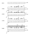
次に、図29を用いて、図28で示した半導体装置100の製造方法について説明する。まず、S101において、半導体基板SUBを用意し、半導体基板SUB上に、不図示の熱検出回路等を構成するMISFET(Metal Insulator Semiconductor Field Effect Transistor)を形成する。   Next, a method for manufacturing the semiconductor device 100 shown in FIG. 28 will be described with reference to FIG. First, in S101, a semiconductor substrate SUB is prepared, and a MISFET (Metal Insulator Semiconductor Field Effect Transistor) constituting a heat detection circuit (not shown) or the like is formed on the semiconductor substrate SUB.

次いで、S102において、S101で形成した半導体基板SUB上に配線構造層L及び最上層配線構造20を形成する。すなわち、半導体基板SUB上に配線層及び層間絶縁膜を含む配線構造層Lを積層形成し、配線構造層L上に最上層配線として、壁配線20a、ヒータ・熱センサ配線110を形成する。層間絶縁膜にはシリコン酸化物もしくはシリコン酸化物に炭素を混入させたものを使用する。   Next, in S102, the wiring structure layer L and the uppermost layer wiring structure 20 are formed on the semiconductor substrate SUB formed in S101. That is, a wiring structure layer L including a wiring layer and an interlayer insulating film is stacked on the semiconductor substrate SUB, and the wall wiring 20a and the heater / thermal sensor wiring 110 are formed on the wiring structure layer L as the uppermost layer wiring. As the interlayer insulating film, silicon oxide or silicon oxide mixed with carbon is used.

次いで、S103において、S102で形成した積層体10の上面全体に保護層21を堆積させる。すなわち、配線構造層L、壁配線20a及びヒータ・熱センサ配線110の上面全体を覆うように保護層21を形成する。ここで保護層21の材料はポリイミドとする。   Next, in S103, the protective layer 21 is deposited on the entire top surface of the laminate 10 formed in S102. That is, the protective layer 21 is formed so as to cover the entire upper surface of the wiring structure layer L, the wall wiring 20a, and the heater / thermal sensor wiring 110. Here, the material of the protective layer 21 is polyimide.

次いで、S104において、S103で形成した積層体10の上面に対し露光を行うことにより、ヒータ・熱センサ配線110周辺の保護層21を除去する。すなわち、壁配線20aの内側における配線構造層L及びヒータ・熱センサ配線110の上面を露光し保護層21を除去することで、配線構造層Lの層間絶縁膜及びヒータ・熱センサ配線110を露出させる。   Next, in S104, the protective layer 21 around the heater / thermal sensor wiring 110 is removed by exposing the upper surface of the laminate 10 formed in S103. That is, by exposing the upper surface of the wiring structure layer L and the heater / thermal sensor wiring 110 inside the wall wiring 20a and removing the protective layer 21, the interlayer insulating film of the wiring structure layer L and the heater / thermal sensor wiring 110 are exposed. Let

次いで、S105において、S104で形成した積層体10の上部に、張り合わせによりカバー板80を接合する。すなわち、保護層21のうち、壁配線20aによって、他の部分よりも突出している部分に、カバー板80を接触させ接合する。以上の工程により、図28の半導体装置100が形成される。   Next, in S105, the cover plate 80 is bonded to the upper portion of the laminate 10 formed in S104 by bonding. That is, the cover plate 80 is brought into contact with and joined to a portion of the protective layer 21 that protrudes from the other portion by the wall wiring 20a. Through the above steps, the semiconductor device 100 of FIG. 28 is formed.

このように、本実施形態の半導体装置では、積層体最上層の壁配線によりガスを封入する空洞部を形成し、空洞部内にヒータと複数の熱センサを配置する。積層体上部の空気をヒータで加熱し、熱センサで温度を検知することにより、半導体装置に加えられた加速度を検出することができる。   As described above, in the semiconductor device according to the present embodiment, the hollow portion that encloses the gas is formed by the wall wiring in the uppermost layer of the stacked body, and the heater and the plurality of thermal sensors are arranged in the hollow portion. The acceleration applied to the semiconductor device can be detected by heating the air above the stacked body with a heater and detecting the temperature with a thermal sensor.

上記のように、図27のような参考例の加速度センサでは、シリコン基板を削り取ってチャンバーを形成し、チャンバーの中空にヒータ及び熱センサを配置する必要があるため、加速度センサの製造が非常に困難であった。本発明では、加速度センサを図28のような半導体装置の構成とすることにより、加速度センサを図29のように一般的な半導体プロセスで製造することができるため、製造効率の向上や高集積化を図ることができる。   As described above, in the acceleration sensor of the reference example as shown in FIG. 27, it is necessary to scrape the silicon substrate to form a chamber, and to arrange a heater and a thermal sensor in the hollow of the chamber. It was difficult. In the present invention, since the acceleration sensor can be manufactured by a general semiconductor process as shown in FIG. 29 by adopting the structure of the semiconductor device as shown in FIG. 28, the manufacturing efficiency is improved and the integration is increased. Can be achieved.

実施の形態15
図30を用いて、本実施形態に係る半導体装置100について説明する。図30(a)及び(b)は、本実施形態に係る半導体装置100の上面断面図及び側面断面図である。
Embodiment 15
The semiconductor device 100 according to this embodiment will be described with reference to FIG. 30A and 30B are a top sectional view and a side sectional view of the semiconductor device 100 according to the present embodiment.

図30の半導体装置100では、図28の半導体装置100と比べて、ヒータ・熱センサ配線110上にカバー膜111が形成されている。その他の構成は、図28と同様である。   In the semiconductor device 100 of FIG. 30, a cover film 111 is formed on the heater / thermal sensor wiring 110 as compared to the semiconductor device 100 of FIG. Other configurations are the same as those in FIG.

すなわち、ヒータ・熱センサ配線110表面の露出部分を、ヒータ・熱センサ用のカバー膜111で囲う。ヒータ・熱センサ配線110のガスに触れる上面及び側面の全体を覆うようにカバー膜111を形成する。カバー膜111の材料には、ポリイミドなどの有機物や、SiOなどの酸化膜、SiN、TiN、TaNなどの窒化膜を使用する。 That is, the exposed portion of the surface of the heater / thermal sensor wiring 110 is surrounded by the cover film 111 for the heater / thermal sensor. A cover film 111 is formed so as to cover the entire upper surface and side surfaces of the heater / thermal sensor wiring 110 that are in contact with the gas. The material of the cover film 111, use or organic materials such as polyimide, an oxide film such as SiO 2, SiN, TiN, a nitride film such as TaN.

上記のように、ヒータ・熱センサ配線110上にカバー膜を形成することにより、ヒータ・熱センサ配線110が直接ガスに触れることがない。したがって、ガスに触れることによるヒータ・熱センサ配線110のメタル材料の腐食、断線を防ぐことができる。   As described above, by forming the cover film on the heater / thermal sensor wiring 110, the heater / thermal sensor wiring 110 does not directly contact the gas. Therefore, corrosion and disconnection of the metal material of the heater / thermal sensor wiring 110 due to contact with the gas can be prevented.

また、カバー膜111は、壁配線20a等の他の部分の保護層(保護膜)よりも薄く形成することが好ましい。カバー膜111を薄膜とすることで、熱伝導がよくなるため、ヒータの発熱効率や熱センサの検出感度を向上することができる。   The cover film 111 is preferably formed thinner than the protective layer (protective film) in other parts such as the wall wiring 20a. By making the cover film 111 a thin film, heat conduction is improved, so that the heat generation efficiency of the heater and the detection sensitivity of the heat sensor can be improved.

実施の形態16
図31を用いて、本実施形態に係る半導体装置100について説明する。図31(a)及び(b)は、本実施形態に係る半導体装置100の上面断面図及び側面断面図である。図31の半導体装置100と図28の半導体装置とを比べると、ヒータ・熱センサ配線110が形成される配線層の階層が異なっており、その他の構成は同様である。図28の半導体装置100では、ヒータ・熱センサ配線110は壁配線20aと同じ最上層に形成されており、図31に示す本実施形態の半導体装置100では、ヒータ・熱センサ配線110は、壁配線20aよりも下層の配線層に形成される。
Embodiment 16
The semiconductor device 100 according to this embodiment will be described with reference to FIG. 31A and 31B are a top sectional view and a side sectional view of the semiconductor device 100 according to this embodiment. When the semiconductor device 100 of FIG. 31 and the semiconductor device of FIG. 28 are compared, the layers of the wiring layer in which the heater / thermal sensor wiring 110 is formed are different, and the other configurations are the same. In the semiconductor device 100 of FIG. 28, the heater / thermal sensor wiring 110 is formed in the same uppermost layer as the wall wiring 20a. In the semiconductor device 100 of this embodiment shown in FIG. It is formed in a wiring layer below the wiring 20a.

例えば、配線構造層Lは、配線構造層L1〜L3を含んでおり、最上層の1つ下層である配線構造層L3(中間層)の配線層に、ヒータ・熱センサ配線110が形成される。壁配線20aの内側では、配線構造層L2の上面まで、積層体の表面が掘り下げられている。   For example, the wiring structure layer L includes wiring structure layers L1 to L3, and the heater / thermal sensor wiring 110 is formed in the wiring layer of the wiring structure layer L3 (intermediate layer) which is one lower layer of the uppermost layer. . Inside the wall wiring 20a, the surface of the laminate is dug down to the upper surface of the wiring structure layer L2.

空洞部24は、上面側をカバー板80に覆われ、底面側を中間層の配線構造層L(L2)の層間絶縁膜に覆われ、側面側を壁配線20a及び最上層に接する配線構造層L(L3)の層間絶縁膜に覆われて封止形成されている。すなわち、図31の空洞部24は、図28の空洞部24に比べて、配線構造層L3の厚さ分だけ深く形成されている。   The cavity 24 is covered with the cover plate 80 on the upper surface side, covered with the interlayer insulating film of the intermediate wiring structure layer L (L2) on the bottom surface side, and the wiring structure layer in contact with the wall wiring 20a and the uppermost layer on the side surface side. It is covered with an L (L3) interlayer insulating film and sealed. That is, the cavity 24 in FIG. 31 is formed deeper than the cavity 24 in FIG. 28 by the thickness of the wiring structure layer L3.

次に、図32を用いて、図31で示した半導体装置100の製造方法について説明する。なお、図32では、図29と比べて、ヒータ・熱センサ配線110の形成位置と、ヒータ・熱センサ配線110を露出するためのエッチング工程とが異なっており、その他については同様である。   Next, a method for manufacturing the semiconductor device 100 shown in FIG. 31 will be described with reference to FIG. 32 is different from FIG. 29 in the formation position of the heater / thermal sensor wiring 110 and the etching process for exposing the heater / thermal sensor wiring 110, and the other is the same.

まず、S201において、半導体基板SUBを用意し、半導体基板SUB上に、不図示の熱検出回路等を構成するMISFETを形成する。   First, in S201, a semiconductor substrate SUB is prepared, and a MISFET constituting a heat detection circuit (not shown) or the like is formed on the semiconductor substrate SUB.

次いで、S202において、S201で形成した半導体基板SUB上に配線構造層L及び最上層配線構造20を形成する。すなわち、半導体基板SUB上に配線層及び層間絶縁膜を含む配線構造層Lを積層形成し、配線構造層L3の配線層に中間層配線としてヒータ・熱センサ配線110を形成する。ヒータ・熱センサ配線110上には層間絶縁膜が形成され、その層間絶縁膜上に、最上層配線として壁配線20aを形成する。   Next, in S202, the wiring structure layer L and the uppermost layer wiring structure 20 are formed on the semiconductor substrate SUB formed in S201. That is, a wiring structure layer L including a wiring layer and an interlayer insulating film is stacked on the semiconductor substrate SUB, and the heater / thermal sensor wiring 110 is formed as an intermediate layer wiring in the wiring layer of the wiring structure layer L3. An interlayer insulating film is formed on the heater / thermal sensor wiring 110, and a wall wiring 20a is formed on the interlayer insulating film as the uppermost layer wiring.

次いで、S203において、S202で形成した積層体10の上面全体に保護層21を堆積させる。すなわち、配線構造層L及び壁配線20a上面全体を覆うように保護層21を形成する。   Next, in S203, the protective layer 21 is deposited on the entire top surface of the laminate 10 formed in S202. That is, the protective layer 21 is formed so as to cover the entire upper surface of the wiring structure layer L and the wall wiring 20a.

次いで、S204において、S203で形成した積層体10の上面に対し露光により、ヒータ・熱センサ配線110の上部周辺の保護層21を除去する。すなわち、壁配線20aの内側における配線構造層Lの上面を露光し保護層21を除去することで、配線構造層Lの層間絶縁膜を露出させる。   Next, in S204, the protective layer 21 around the upper part of the heater / thermal sensor wiring 110 is removed by exposing the upper surface of the laminate 10 formed in S203. That is, the upper surface of the wiring structure layer L inside the wall wiring 20a is exposed to remove the protective layer 21, thereby exposing the interlayer insulating film of the wiring structure layer L.

次いで、S205において、S204で形成した積層体10の上面に対し、保護層21をマスクとして、配線構造層Lの層間絶縁膜をドライエッチングにより除去する。すなわち、壁配線20aの内側について、配線構造層L3の層間絶縁膜をエッチングし、配線構造層L3の配線層であるヒータ・熱センサ配線110と、配線構造層L2の層間絶縁膜とを露出させる。   Next, in S205, with respect to the upper surface of the stacked body 10 formed in S204, the interlayer insulating film of the wiring structure layer L is removed by dry etching using the protective layer 21 as a mask. That is, the inner layer insulating film of the wiring structure layer L3 is etched inside the wall wiring 20a to expose the heater / thermal sensor wiring 110 that is the wiring layer of the wiring structure layer L3 and the interlayer insulating film of the wiring structure layer L2. .

次いで、S206において、S205で形成した積層体10の上部に、張り合わせによりカバー板80を接合する。以上の工程により、図31の半導体装置100が形成される。   Next, in S206, the cover plate 80 is bonded to the upper part of the laminate 10 formed in S205 by bonding. Through the above steps, the semiconductor device 100 of FIG. 31 is formed.

このように、本実施形態の半導体装置では、積層体最上層の壁配線及び下層の層間絶縁膜による段差でガスを封入する空洞部を形成した。この空洞部内にヒータと複数の熱センサを配置し、積層体上部の空気をヒータで加熱して熱センサで温度を検知することにより、図28と同様に、半導体装置の移動速度を検出することができる。また、図29と同様に、一般的な半導体プロセスにより加速度センサを製造することができる。   As described above, in the semiconductor device of this embodiment, the hollow portion that encloses the gas is formed by the step due to the uppermost wall wiring of the stacked body and the lower interlayer insulating film. The moving speed of the semiconductor device can be detected in the same manner as in FIG. 28 by arranging a heater and a plurality of heat sensors in the cavity, and heating the air above the stack with the heater and detecting the temperature with the heat sensor. Can do. Similarly to FIG. 29, the acceleration sensor can be manufactured by a general semiconductor process.

さらに、ヒータ・熱センサ配線110を、掘り下げた配線構造層Lに形成することにより、空洞部24をより広くすることができる。本実施形態では、壁配線20aの厚みや上面視の面積が図28と同様であっても、空洞部24の容積を図28よりも大きくすることができる。空洞部が狭いとガスが流れ難くなるため、空洞部を広くすることによって、ガスが流れやすくなり、加速度センサの感度を向上することができる。   Furthermore, by forming the heater / thermal sensor wiring 110 in the wiring structure layer L that has been dug down, the cavity 24 can be made wider. In the present embodiment, the volume of the cavity 24 can be made larger than that in FIG. 28 even if the thickness of the wall wiring 20a and the area in top view are the same as those in FIG. Since the gas is difficult to flow when the hollow portion is narrow, the gas can easily flow by widening the hollow portion, and the sensitivity of the acceleration sensor can be improved.

実施の形態17
図33を用いて、本実施形態に係る半導体装置100について説明する。図33(a)及び(b)は、本実施形態に係る半導体装置100の上面断面図及び側面断面図である。
Embodiment 17
The semiconductor device 100 according to this embodiment will be described with reference to FIG. 33A and 33B are a top sectional view and a side sectional view of the semiconductor device 100 according to the present embodiment.

図33の半導体装置100では、図31の半導体装置100と比べて、壁配線20aの配置パターン及び壁配線20aにより区画されて形成される空洞部24の形状が異なっている。その他の構成については、図31と同様である。図33の半導体装置100では、図31の半導体装置100と同様に、ヒータ・熱センサ配線110は、最上層よりも下層の配線層に形成されている。これにより、ヒータ・熱センサ配線110の上部にガスを流すための空間を広く設けることが出来る。   The semiconductor device 100 of FIG. 33 differs from the semiconductor device 100 of FIG. 31 in the arrangement pattern of the wall wiring 20a and the shape of the cavity 24 formed by being partitioned by the wall wiring 20a. Other configurations are the same as those in FIG. In the semiconductor device 100 of FIG. 33, similarly to the semiconductor device 100 of FIG. 31, the heater / thermal sensor wiring 110 is formed in a lower wiring layer than the uppermost layer. As a result, a large space for flowing gas can be provided above the heater / thermal sensor wiring 110.

本実施形態における、壁配線20aの配置パターンにより形成される空洞部24の形状について説明する。図31の半導体装置100では、空洞部24の上面断面がY方向を長辺方向とする略長方形状であり、キャビティ23aからガス流路22を介してキャビティ23bまでの上面断面の幅が同じである。   The shape of the cavity 24 formed by the arrangement pattern of the wall wiring 20a in the present embodiment will be described. In the semiconductor device 100 of FIG. 31, the cross section of the upper surface of the cavity portion 24 is substantially rectangular with the Y direction as the long side direction, and the width of the upper surface cross section from the cavity 23a to the cavity 23b through the gas flow path 22 is the same. is there.

これに対し、図33に示す本実施形態の半導体装置100では、空洞部24は、熱センサ30,50の近傍と他の部分とで、上面断面のX方向(ガスの流れと垂直方向)の幅が大きく異なる。すなわち、熱センサ30,50が配置されているガス流路22では幅が狭く、ガス流路22の両側に幅の広いキャビティ23a、23bが形成されている。   On the other hand, in the semiconductor device 100 of the present embodiment shown in FIG. 33, the cavity 24 is in the vicinity of the thermal sensors 30 and 50 and in other parts in the X direction (perpendicular to the gas flow) in the upper surface cross section. The width varies greatly. That is, the gas flow path 22 in which the thermal sensors 30 and 50 are disposed has a narrow width, and wide cavities 23 a and 23 b are formed on both sides of the gas flow path 22.

図33では、キャビティ23a、23bは、上面断面がX方向を長辺方向とする略長方形状であり、長辺の長さが、ガス流路22の幅よりも長い。なお、キャビティ23a、23bは、ガス流路22よりも幅が広ければよいため、長方形に限らず、略正方形でもよいし、その他の多角形状等であってもよい。また、少なくとも、熱センサ30、50の近傍において、ガス流路22の幅が狭くなればよい。例えば、ヒータ40の近傍が、熱センサ30、50の近傍よりも、幅が広くなっていてもよい。   In FIG. 33, the cavities 23 a and 23 b have a substantially rectangular shape in which the top cross section has the X direction as the long side direction, and the length of the long side is longer than the width of the gas flow path 22. The cavities 23a and 23b need only be wider than the gas flow path 22. Therefore, the cavities 23a and 23b are not limited to a rectangle but may be a substantially square shape or other polygonal shapes. Further, at least in the vicinity of the thermal sensors 30 and 50, the width of the gas flow path 22 may be narrowed. For example, the vicinity of the heater 40 may be wider than the vicinity of the thermal sensors 30 and 50.

半導体装置100が移動すると、空洞部24内のガスは半導体装置100の動きに追従できないため、半導体装置100の動きと逆の方向にガスの流れが発生する。キャビティ23aのガスがキャビティ23bへ移動するには、熱センサ30,50近傍のガス流路22を通る必要がある。広い空間であるキャビティ23aのガスが、狭い空間(隘路)のガス流路22を通過しようとすると、体積の大きいガスが狭い隘路に急激に入り込むためガスの圧力が高まる。   When the semiconductor device 100 moves, the gas in the cavity 24 cannot follow the movement of the semiconductor device 100, and thus a gas flow is generated in the direction opposite to the movement of the semiconductor device 100. In order for the gas in the cavity 23a to move to the cavity 23b, it is necessary to pass through the gas flow path 22 in the vicinity of the thermal sensors 30 and 50. When the gas in the cavity 23a, which is a large space, tries to pass through the gas passage 22 in the narrow space (bottle), the gas pressure increases because the gas having a large volume rapidly enters the narrow bottleneck.

したがって、ガス流路22を通るときのガスの流速は、キャビティ23a、23bの部分よりも速くなる。ガス流路22においてガスの流速が速くなると、ガスの流れによって熱も速く伝わり、かつ、伝わる熱量も大きくなる。よって、狭い隘路が無い場合に比べると、センサの温度変化がより速く、かつ、より大きくなるため、加速度センサの感度を高めることが出来る。   Therefore, the flow rate of the gas when passing through the gas flow path 22 is faster than that of the cavities 23a and 23b. When the flow velocity of the gas is increased in the gas flow path 22, heat is transferred quickly by the gas flow, and the amount of heat transferred is increased. Therefore, the sensitivity of the acceleration sensor can be increased because the temperature change of the sensor is faster and larger than when there is no narrow bottleneck.

上記のように、図27の参考例や図31等のような加速度センサでは、熱センサの部分と他の部分とでガスを密閉する空洞部の形状に変化はなく、ガスの流速にも変化はなかった。したがって、ガスの流速を制御することはできず、加速度センサの感度を向上させるためには、空洞部やヒータ・熱センサ配線を大きくする必要があった。   As described above, in the acceleration sensor as shown in the reference example of FIG. 27, FIG. 31, etc., the shape of the cavity that seals the gas between the thermal sensor and the other part does not change, and the flow rate of the gas also changes. There was no. Therefore, the flow rate of the gas cannot be controlled, and in order to improve the sensitivity of the acceleration sensor, it is necessary to enlarge the cavity and the heater / heat sensor wiring.

本実施形態では、積層体上部のガスの流れを検出する加速度センサにおいて、ガスの流れる領域を局所的に狭くすることで、その部分のガスの流速を他の部分よりも速くする。この流速の速い部分に熱センサを配置することで、ガスの温度の検出感度を高めることができる。   In this embodiment, in the acceleration sensor that detects the gas flow in the upper part of the stacked body, the gas flow region is locally narrowed so that the flow velocity of the gas in that portion is faster than in other portions. By arranging the thermal sensor in the portion where the flow velocity is fast, the detection sensitivity of the gas temperature can be increased.

実施の形態18
図34を用いて、本実施形態に係る半導体装置100について説明する。図34(a)及び(b)は、本実施形態に係る半導体装置100の上面断面図及び側面断面図である。
Embodiment 18
The semiconductor device 100 according to this embodiment will be described with reference to FIG. 34A and 34B are a top sectional view and a side sectional view of the semiconductor device 100 according to this embodiment.

図34の半導体装置100では、図33の半導体装置100と比べて、壁配線20aの配置パターン及び壁配線20aにより区画されて形成される空洞部24のうちのキャビティの形状が異なっている。その他の構成については、図33と同様である。   The semiconductor device 100 of FIG. 34 differs from the semiconductor device 100 of FIG. 33 in the arrangement pattern of the wall wirings 20a and the shape of the cavities 24 of the cavity portions 24 that are defined by the wall wirings 20a. Other configurations are the same as those in FIG.

図33の半導体装置100では、キャビティ23a、23bがX方向を長辺方向とする略長方形状である。ガス流路22の辺(壁配線)に対し、キャビティ23a、23bの辺(壁配線)が直角に接している。   In the semiconductor device 100 of FIG. 33, the cavities 23a and 23b have a substantially rectangular shape with the X direction as the long side direction. The sides (wall wiring) of the cavities 23a and 23b are in contact with the side (wall wiring) of the gas flow path 22 at a right angle.

これに対し、図34の本実施形態の半導体装置100では、ガス流路22の辺(壁配線)に対し、キャビティ23a、23bの辺(壁配線)が、直角よりも緩やかな角度で接している。すなわち、壁配線20aにより形成される空洞部24の幅が、熱センサ30,50を配置するガス流路22近傍が最も狭く、熱センサ30,50から離れるに従って徐々に広くなっている。また、空洞部24の幅が、熱センサ30,50から最も遠い部分が最も広く、熱センサ30,50に近づくに従って徐々に狭くなっているとも言える。少なくとも、ガス流路22に接するキャビティ23a、23bの辺が、X方向(ガスの流れる方向)に対し、斜めであればよく、キャビティ23a、23bの形状は、どのような形状であってもよい。   On the other hand, in the semiconductor device 100 of this embodiment shown in FIG. 34, the sides (wall wiring) of the cavities 23a and 23b are in contact with the sides (wall wiring) of the gas flow path 22 at a gentler angle than the right angle. Yes. That is, the width of the cavity 24 formed by the wall wiring 20a is the narrowest in the vicinity of the gas flow path 22 in which the thermal sensors 30 and 50 are disposed, and gradually increases as the distance from the thermal sensors 30 and 50 increases. Further, it can be said that the width of the cavity 24 is the widest at the portion farthest from the thermal sensors 30 and 50 and gradually becomes narrower as the thermal sensors 30 and 50 are approached. At least the sides of the cavities 23a and 23b in contact with the gas flow path 22 may be oblique with respect to the X direction (the direction of gas flow), and the cavities 23a and 23b may have any shape. .

このように、本実施形態では、キャビティの形状を熱センサに近づくに従って徐々に変化するようにした。これにより、図33のようにキャビティの角がガス流路に対し直角な形状の場合よりも空気抵抗が小さくなり、ガスの流れがスムーズとなるため、加速度センサの感度をより向上することができる。例えば、空洞部24に封入される物質が、壁配線による抵抗を受けやすい物の場合、キャビティの辺をガス流路に対し斜めにし、空気抵抗を減らすことで、流れを大幅に速くすることができる。   Thus, in this embodiment, the shape of the cavity is gradually changed as it approaches the thermal sensor. As a result, the air resistance becomes smaller and the gas flow becomes smoother than in the case where the corner of the cavity is perpendicular to the gas flow path as shown in FIG. 33, so that the sensitivity of the acceleration sensor can be further improved. . For example, when the substance enclosed in the cavity 24 is easily subject to resistance due to wall wiring, the flow can be greatly increased by making the sides of the cavity oblique to the gas flow path and reducing the air resistance. it can.

実施の形態19
図33や図34では、空洞部24の上面断面の形状が熱センサ近傍で変化する例について説明した。本実施形態では、空洞部24の側面断面の形状が熱センサ近傍で変化する例について説明する。
Embodiment 19
In FIG. 33 and FIG. 34, the example in which the shape of the upper surface cross section of the cavity 24 changes in the vicinity of the thermal sensor has been described. In the present embodiment, an example will be described in which the shape of the side cross section of the cavity 24 changes in the vicinity of the thermal sensor.

図35(a)及び(b)は、本実施形態に係る半導体装置100の上面断面図及び側面断面図である。   35A and 35B are a top sectional view and a side sectional view of the semiconductor device 100 according to this embodiment.

図35の半導体装置100では、図28や図31の半導体装置100と比べて、ヒータもしくは熱センサが形成される配線層の位置(階層)が異なっている。その他の構成については、図28や図31と同様である。   The semiconductor device 100 of FIG. 35 differs from the semiconductor device 100 of FIGS. 28 and 31 in the position (layer) of the wiring layer in which the heater or the thermal sensor is formed. Other configurations are the same as those in FIGS. 28 and 31.

図28や図31の半導体装置100では、ヒータ40と熱センサ30、50とは、同じ配線層に形成されている。これに対し、図35の本実施形態の半導体装置100では、ヒータ40と熱センサ30、50とは、別の配線層に形成される。   In the semiconductor device 100 of FIGS. 28 and 31, the heater 40 and the thermal sensors 30 and 50 are formed in the same wiring layer. On the other hand, in the semiconductor device 100 of the present embodiment shown in FIG. 35, the heater 40 and the thermal sensors 30 and 50 are formed in different wiring layers.

図35に示すように、熱センサ30、50は壁配線20aと同じ最上層に形成され、ヒータ40は、壁配線20aよりも下の配線構造層Lに形成される。例えば、配線構造層Lは、配線構造層L1〜L3を含んでおり、最上層の1つ下層である配線構造層L3(中間層)の配線層に、ヒータ40が形成される。熱センサ30と熱センサ50に挟まれたヒータ40近傍では、配線構造層L2の層間絶縁膜上面まで、積層体の表面が掘り下げられている。すなわち、ヒータ40近傍では、空洞部24のZ方向の深さが深く、熱センサ30、50近傍では、空洞部24のZ方向の深さが浅くなっている。   As shown in FIG. 35, the thermal sensors 30 and 50 are formed in the same uppermost layer as the wall wiring 20a, and the heater 40 is formed in the wiring structure layer L below the wall wiring 20a. For example, the wiring structure layer L includes wiring structure layers L1 to L3, and the heater 40 is formed in the wiring layer of the wiring structure layer L3 (intermediate layer), which is one lowermost layer. In the vicinity of the heater 40 sandwiched between the thermal sensor 30 and the thermal sensor 50, the surface of the stacked body is dug down to the upper surface of the interlayer insulating film of the wiring structure layer L2. That is, in the vicinity of the heater 40, the depth of the cavity 24 in the Z direction is deep, and in the vicinity of the thermal sensors 30, 50, the depth of the cavity 24 in the Z direction is shallow.

このように、本実施形態では、熱センサ30,50を最上層に形成し、ヒータ40を最上層より掘り下げた下層の配線層に形成するようにした。これにより、空洞部の空間が、ヒータ40近傍で広くなり、熱センサ30,50近傍で狭くなる。したがって、図33や図34と同様に、熱センサ近傍におけるガスの流速を速くすることができ、加速度センサの感度を向上することができる。   Thus, in this embodiment, the thermal sensors 30 and 50 are formed in the uppermost layer, and the heater 40 is formed in the lower wiring layer dug down from the uppermost layer. As a result, the space of the cavity becomes wider near the heater 40 and becomes narrow near the thermal sensors 30 and 50. Therefore, similarly to FIG. 33 and FIG. 34, the gas flow velocity in the vicinity of the thermal sensor can be increased, and the sensitivity of the acceleration sensor can be improved.

実施の形態20
本実施形態では、空洞部24の側面断面の形状が熱センサ近傍で変化する他の例について説明する。図36(a)及び(b)は、本実施形態に係る半導体装置100の上面断面図及び側面断面図である。
Embodiment 20
In the present embodiment, another example in which the shape of the side cross section of the cavity 24 changes in the vicinity of the thermal sensor will be described. 36A and 36B are a top sectional view and a side sectional view of the semiconductor device 100 according to the present embodiment.

図36の半導体装置100では、図28の半導体装置100と比べて、キャビティが接する層が異なっている。また、図36の半導体装置100では、図31の半導体装置100と比べて、ヒータ・熱センサ配線が形成される層の位置が異なっている。その他の構成については、図28や図31と同様である。   The semiconductor device 100 in FIG. 36 differs from the semiconductor device 100 in FIG. 28 in the layer in contact with the cavity. 36 differs from the semiconductor device 100 of FIG. 31 in the position of the layer where the heater / thermal sensor wiring is formed. Other configurations are the same as those in FIGS. 28 and 31.

図28や図31の半導体装置100では、ヒータ・熱センサ配線110が配置される配線層と、キャビティ23a、23bが接する層とが同じ階層である。これに対し、図36の本実施形態の半導体装置100では、ヒータ・熱センサ配線110が配置される配線層と、キャビティ23a、23bが接する層とが、別の階層である。   In the semiconductor device 100 of FIGS. 28 and 31, the wiring layer in which the heater / thermal sensor wiring 110 is disposed and the layer in contact with the cavities 23a and 23b are on the same level. On the other hand, in the semiconductor device 100 of this embodiment shown in FIG. 36, the wiring layer in which the heater / thermal sensor wiring 110 is disposed and the layer in contact with the cavities 23a and 23b are in different layers.

図36に示すように、ヒータ・熱センサ配線110は壁配線20aと同じ最上層に形成されている。キャビティ23a、23bは壁配線20aよりも下層の配線構造層Lに接している。例えば、配線構造層Lは、配線構造層L1〜L3を含んでおり、壁配線20aと熱センサ30、50とに挟まれたキャビティ23a、23bでは、配線構造層L2の層間絶縁膜上面まで、積層体の表面が掘り下げられている。すなわち、キャビティ23a、23b近傍では、空洞部24のZ方向の深さが深く、熱センサ30、50近傍では、空洞部24のZ方向の深さが浅くなっている。   As shown in FIG. 36, the heater / thermal sensor wiring 110 is formed on the same uppermost layer as the wall wiring 20a. The cavities 23a and 23b are in contact with the wiring structure layer L below the wall wiring 20a. For example, the wiring structure layer L includes the wiring structure layers L1 to L3. In the cavities 23a and 23b sandwiched between the wall wiring 20a and the thermal sensors 30 and 50, up to the upper surface of the interlayer insulating film of the wiring structure layer L2, The surface of the laminate is dug down. That is, the depth in the Z direction of the cavity 24 is deep in the vicinity of the cavities 23a and 23b, and the depth in the Z direction of the cavity 24 is shallow in the vicinity of the thermal sensors 30 and 50.

このように、本実施形態では、ヒータ・熱センサ配線110を最上層に形成し、キャビティ23a、23bに接する配線構造層を下層まで掘り下げるようにした。これにより、空洞部の空間が、キャビティ23a、23b近傍で広く、熱センサ30,50近傍で狭くなる。したがって、図35と同様に、熱センサ近傍におけるガスの流速を速くすることができ、加速度センサの感度を向上することができる。   Thus, in this embodiment, the heater / thermal sensor wiring 110 is formed in the uppermost layer, and the wiring structure layer in contact with the cavities 23a and 23b is dug down to the lower layer. Thereby, the space of the cavity is wide near the cavities 23 a and 23 b and narrow near the thermal sensors 30 and 50. Therefore, similarly to FIG. 35, the gas flow velocity in the vicinity of the thermal sensor can be increased, and the sensitivity of the acceleration sensor can be improved.

実施の形態21
本実施形態では、空洞部24の上面断面の形状が熱センサ近傍で変化する他の例について説明する。図37は、本実施形態に係る半導体装置100の上面断面図である。なお、半導体装置100の側面断面図については、図33(b)等と同様である。
Embodiment 21
In the present embodiment, another example in which the shape of the upper surface cross section of the cavity 24 changes in the vicinity of the thermal sensor will be described. FIG. 37 is a top cross-sectional view of the semiconductor device 100 according to the present embodiment. Note that a side sectional view of the semiconductor device 100 is the same as FIG.

図33の半導体装置100では、X方向に延びるガス流路を形成し、その両端にキャビティを形成している。これに対し、図37の本実施形態の半導体装置100では、図33の構成に加えて、Y方向に延びるガス流路を形成し、その両端にキャビティを形成する。   In the semiconductor device 100 of FIG. 33, a gas flow path extending in the X direction is formed, and cavities are formed at both ends thereof. On the other hand, in the semiconductor device 100 of the present embodiment of FIG. 37, in addition to the configuration of FIG. 33, a gas flow path extending in the Y direction is formed, and cavities are formed at both ends thereof.

図37に示すように、ヒータ40を中心に配置し、そのX方向及びY方向に隣接して4つの熱センサ30(50)を配置する。Y方向では、熱センサ30a(50)、ヒータ40、熱センサ30b(50)の順に並ぶように配置し、X方向では、熱センサ30c(50)、ヒータ40、熱センサ30d(50)の順に並ぶように配置する。   As shown in FIG. 37, the heater 40 is arranged at the center, and the four thermal sensors 30 (50) are arranged adjacent to the X direction and the Y direction. In the Y direction, the heat sensor 30a (50), the heater 40, and the heat sensor 30b (50) are arranged in this order. In the X direction, the heat sensor 30c (50), the heater 40, and the heat sensor 30d (50) are arranged in this order. Arrange them side by side.

熱センサ30a、30bの配置される位置に、Y方向に延びるガス流路22a、22bが形成される。ガス流路22aとガス流路22bとからガス流路22yが構成され、ガス流路22yの両端にキャビティ23a、23bが形成される。   Gas flow paths 22a and 22b extending in the Y direction are formed at positions where the thermal sensors 30a and 30b are arranged. A gas flow path 22y is constituted by the gas flow path 22a and the gas flow path 22b, and cavities 23a and 23b are formed at both ends of the gas flow path 22y.

また、熱センサ30c、30dの配置される位置に、X方向に延びるガス流路22c、22dが形成される。ガス流路22cとガス流路22dとからガス流路22xが構成され、ガス流路22xの両端にキャビティ23c、23dが形成される。   In addition, gas flow paths 22c and 22d extending in the X direction are formed at positions where the thermal sensors 30c and 30d are disposed. A gas flow path 22x is constituted by the gas flow path 22c and the gas flow path 22d, and cavities 23c and 23d are formed at both ends of the gas flow path 22x.

ガス流路22yとガス流路22xは、十字型に直交交差し、ガス流路が交差する位置にヒータ40が配置されるとも言える。ヒータ40から一定距離の各ガス流路内に4つの熱センサ30が配置されている。なお、キャビティの形状は、図33や図34と同様にその他の形状であってもよい。   It can be said that the gas flow path 22y and the gas flow path 22x intersect at right angles in a cross shape, and the heater 40 is disposed at a position where the gas flow paths intersect. Four thermal sensors 30 are arranged in each gas flow path at a constant distance from the heater 40. The shape of the cavity may be other shapes as in FIG. 33 and FIG.

このように、本実施形態では、X方向にヒータを挟むように熱センサを配置するとともに、Y方向にヒータを挟むように熱センサを配置することにより、図26と同様に、4つ熱センサでX方向及びY方向の2軸の加速度を検出することができる。   As described above, in this embodiment, the thermal sensor is arranged so as to sandwich the heater in the X direction, and the thermal sensor is arranged so that the heater is sandwiched in the Y direction, so that four thermal sensors are arranged as in FIG. Thus, the biaxial acceleration in the X direction and the Y direction can be detected.

また、本実施形態では、空洞部の幅を、4つの熱センサの配置されるX方向及びY方向のガス流路部分では狭く、その外側の4つのキャビティでは広くしている。これにより、図33等と同様に、ガス流路部分のガスの流速を速くすることができ、加速度センサとしての感度を高めることが出来る。   Further, in the present embodiment, the width of the cavity is narrow in the gas flow path portions in the X direction and the Y direction where the four thermal sensors are arranged, and wide in the four cavities outside the cavity. Thereby, similarly to FIG. 33 etc., the flow velocity of the gas of a gas flow-path part can be made quick, and the sensitivity as an acceleration sensor can be improved.

実施の形態22
図38を用いて、本実施形態に係るヒータ・熱センサ配線110の配線パターンについて説明する。図38は、ヒータ40もしくは熱センサ30,50の上面視の配線パターンである。
Embodiment 22
A wiring pattern of the heater / thermal sensor wiring 110 according to the present embodiment will be described with reference to FIG. FIG. 38 is a wiring pattern in the top view of the heater 40 or the thermal sensors 30 and 50.

上述のように半導体装置100では、ヒータ40及び熱センサ30,50はメタルの配線で構成され、配線の寄生抵抗を利用することによりヒータ及び熱センサとして動作する。このため、ヒータ40及び熱センサ30,50を効果的に動作させるためには、メタル配線の抵抗値を大きくする必要がある。   As described above, in the semiconductor device 100, the heater 40 and the thermal sensors 30, 50 are configured by metal wiring, and operate as a heater and a thermal sensor by utilizing the parasitic resistance of the wiring. For this reason, in order to operate the heater 40 and the thermal sensors 30 and 50 effectively, it is necessary to increase the resistance value of the metal wiring.

そこで、配線の抵抗値を大きくするため、図38に示すように、本実施形態では、ヒータ・熱センサ配線110を細長く配置する。図38は、ミアンダ形状の配線の3つの配線パターン例を示している。   Therefore, in order to increase the resistance value of the wiring, as shown in FIG. 38, in this embodiment, the heater / thermal sensor wiring 110 is elongated. FIG. 38 shows three wiring pattern examples of meander-shaped wiring.

図38に示すように、ヒータ・熱センサ配線110をミアンダ形状に配置することで、細長い配線を狭い面積に効率よく配置することができる。ミアンダ形状の配線とは、ジグザグ状の配線パターンの配線であり、一方向と反対の他方向とに交互に折り返しながら敷設された配線である。   As shown in FIG. 38, by arranging the heater / thermal sensor wiring 110 in a meander shape, it is possible to efficiently arrange the elongated wiring in a narrow area. The meander-shaped wiring is a wiring having a zigzag wiring pattern, and is a wiring laid while being alternately folded back in one direction and the other direction.

図38(a)、(b)は、Y軸正方向及びY軸負方向(ガスの流れる方向)に向かって左右非対称の配線パターンであり、図38(c)は、Y軸正方向及びY軸負方向に向かって左右対称の配線パターンである。   FIGS. 38A and 38B are asymmetrical wiring patterns in the Y-axis positive direction and the Y-axis negative direction (gas flow direction), and FIG. 38C shows the Y-axis positive direction and the Y-axis positive direction. It is a wiring pattern that is symmetrical in the left-right direction.

図38(a)の配線パターン120では、ヒータ・熱センサ配線110は、ミアンダ形状のミアンダ配線部110aと直線状の戻り配線部110bとを有している。配線パターン120では、Y軸方向正側に、ミアンダ配線部110aが配置され、Y軸方向負側に、戻り配線部110bが配置されている。   In the wiring pattern 120 of FIG. 38A, the heater / thermal sensor wiring 110 has a meander-shaped meander wiring portion 110a and a linear return wiring portion 110b. In the wiring pattern 120, the meander wiring part 110a is arranged on the Y axis direction positive side, and the return wiring part 110b is arranged on the Y axis direction negative side.

ミアンダ配線部110aは、一端が太幅配線113aを介してトレンチ配線(ビア)112aに接続され、他端が戻り配線部110bに接続される。ミアンダ配線部110aは、ガスの流れる方向(Y方向)に沿って延在配置する配線を交互に折り返しながら形成される。   The meander wiring portion 110a has one end connected to the trench wiring (via) 112a via the thick wiring 113a and the other end connected to the return wiring portion 110b. The meander wiring portion 110a is formed by alternately folding back wirings that extend along the gas flow direction (Y direction).

戻り配線部110bは、一端がミアンダ配線部110aに接続され、他端が太幅配線113bを介してトレンチ配線112bに接続される。戻り配線部110bは、ガスの流れる方向と直交する方向(X方向)に向かって、ミアンダ配線部110aの他端から、トレンチ配線112a近傍のトレンチ配線112bまで直線状に延在配置される。   The return wiring portion 110b has one end connected to the meander wiring portion 110a and the other end connected to the trench wiring 112b via the thick wiring 113b. The return wiring portion 110b is linearly extended from the other end of the meander wiring portion 110a to the trench wiring 112b in the vicinity of the trench wiring 112a in a direction (X direction) orthogonal to the gas flow direction.

例えば、配線パターン120を実際に形成する場合の一例として、配線材料を銅とし、配線幅0.2μm、配線間隔0.2μm、膜厚0.3μm、配線長1m、抵抗値は700Ωとする。このとき、配線パターン120全体のX方向の長さを50μm、Y方向の長さを15μmとして形成する。   For example, as an example when the wiring pattern 120 is actually formed, the wiring material is copper, the wiring width is 0.2 μm, the wiring interval is 0.2 μm, the film thickness is 0.3 μm, the wiring length is 1 m, and the resistance value is 700Ω. At this time, the entire wiring pattern 120 is formed with a length in the X direction of 50 μm and a length in the Y direction of 15 μm.

図38(b)の配線パターン121では、配線パターン120と同様のミアンダ配線部110aと戻り配線部110bとを有している。配線パターン121では、ミアンダ配線部110a及び戻り配線部110bの配置位置が、配線パターン120と反対になっている。すなわち、Y軸方向負側に、ミアンダ配線部110aが配置され、Y軸方向正側に、戻り配線部110bが配置されている。   The wiring pattern 121 of FIG. 38B has a meander wiring portion 110a and a return wiring portion 110b similar to the wiring pattern 120. In the wiring pattern 121, the arrangement positions of the meander wiring part 110 a and the return wiring part 110 b are opposite to the wiring pattern 120. That is, the meander wiring portion 110a is disposed on the Y axis direction negative side, and the return wiring portion 110b is disposed on the Y axis direction positive side.

図38(c)の配線パターン122では、ヒータ・熱センサ配線110は、2つのミアンダ配線部110a、110cを有している。2つのミアンダ配線部110a、110cがY方向に並んで配置される。   In the wiring pattern 122 of FIG. 38C, the heater / thermal sensor wiring 110 has two meander wiring portions 110a and 110c. Two meander wiring portions 110a and 110c are arranged side by side in the Y direction.

一方のミアンダ配線部110aは、一端が太幅配線113aを介してトレンチ配線112aに接続され、他端がミアンダ配線部110cに接続される。同様に他方のミアンダ配線部110cは、一端が太幅配線113bを介してトレンチ配線112bに接続され、他端がミアンダ配線部110aに接続される。   One meander wiring portion 110a has one end connected to the trench wiring 112a via the thick wiring 113a and the other end connected to the meander wiring portion 110c. Similarly, the other meander wiring portion 110c has one end connected to the trench wiring 112b via the thick wiring 113b and the other end connected to the meander wiring portion 110a.

このように、ヒータ40、熱センサ30,50を構成するヒータ・熱センサ配線110をミアンダ形状に配置することにより、効率よく配線を敷設することができる。そして、配線が延在配置される方向(長辺方向)をガスの流れる方向と平行になるようにすることで、配線によるガスの流れの乱れが低減するため、ガスの流れを乱すことが無くなり、加速度センサの感度を向上することができる。   Thus, by arranging the heater / thermal sensor wiring 110 constituting the heater 40 and the thermal sensors 30, 50 in a meander shape, the wiring can be laid efficiently. And by making the direction (long side direction) in which the wiring extends and parallel to the gas flow direction, the disturbance of the gas flow due to the wiring is reduced, the gas flow is not disturbed. The sensitivity of the acceleration sensor can be improved.

また、ヒータ・熱センサ配線と他の回路の間をつなぐ接続配線は、ヒータ・熱センサ配線よりも下層のメタル配線とし、ヒータ・熱センサ配線と下層の配線とはトレンチ配線を介して接続する。ヒータ・熱センサ配線以外の配線は、下層配線としガスに露出しないようにすることで、ガスの流れに対する影響を抑え、加速度センサの感度向上を図ることができる。   The connection wiring that connects between the heater / thermal sensor wiring and other circuits is a metal wiring below the heater / thermal sensor wiring, and the heater / thermal sensor wiring and the lower wiring are connected via a trench wiring. . Wiring other than the heater / thermal sensor wiring is formed as a lower layer wiring so as not to be exposed to the gas, thereby suppressing the influence on the gas flow and improving the sensitivity of the acceleration sensor.

さらに、ヒータ・熱センサ配線は、トレンチ配線との接続部分の幅を、他の部分の幅よりも太くする。これにより、トレンチ配線部分のEM(Electro Migration)耐性を保つことができる。   Further, in the heater / thermal sensor wiring, the width of the connection portion with the trench wiring is made wider than the width of the other portions. Thereby, EM (Electro Migration) tolerance of the trench wiring part can be maintained.

実施の形態23
図39を用いて、本実施形態に係るヒータ・熱センサ配線110の配線パターンの組み合わせについて説明する。図39は、ヒータ40及び熱センサ30,50の上面視の配線パターンであり、図38で示した配線パターン120〜122を半導体装置100に適用する場合の配線パターンの組み合わせの例を示している。
Embodiment 23
A combination of wiring patterns of the heater / thermal sensor wiring 110 according to the present embodiment will be described with reference to FIG. FIG. 39 is a top view wiring pattern of the heater 40 and the thermal sensors 30 and 50, and shows an example of a combination of wiring patterns when the wiring patterns 120 to 122 shown in FIG. 38 are applied to the semiconductor device 100. .

図39(a)は、ヒータ40を、配線パターン122による配線とし、熱センサ30を、配線パターン120による配線とし、熱センサ50を、配線パターン121による配線とした例である。図39(b)は、ヒータ40を、配線パターン122による配線とし、熱センサ30を、配線パターン121による配線とし、熱センサ50を、配線パターン120による配線とした例である。   FIG. 39A shows an example in which the heater 40 is a wiring by the wiring pattern 122, the thermal sensor 30 is a wiring by the wiring pattern 120, and the thermal sensor 50 is a wiring by the wiring pattern 121. FIG. 39B shows an example in which the heater 40 is a wiring by the wiring pattern 122, the thermal sensor 30 is a wiring by the wiring pattern 121, and the thermal sensor 50 is a wiring by the wiring pattern 120.

ヒータ40は、熱センサ30、50に向かって、ほぼ等しく熱を伝える必要があるため、ガスの流れる方向に向かって左右対象な配線パターン122を採用することが好ましい。   Since the heater 40 needs to transmit heat almost equally toward the heat sensors 30 and 50, it is preferable to employ the left and right wiring patterns 122 in the gas flow direction.

熱センサ30、50は、ヒータ40から発生される熱を、同程度の感度で検出する必要があるため、ヒータ40から見て対象となる配線パターンが好ましい。すなわち、図39(a)では、熱センサ30,50は、ヒータ40に近い側にミアンダ配線部110aが配置され、ヒータ40から遠い側に戻り配線部110bが配置されており、ヒータ40から見て対象になっている。   Since it is necessary for the heat sensors 30 and 50 to detect the heat generated from the heater 40 with the same degree of sensitivity, a wiring pattern to be viewed from the heater 40 is preferable. That is, in FIG. 39A, the thermal sensors 30 and 50 have the meander wiring portion 110 a disposed on the side closer to the heater 40, and the return wiring portion 110 b disposed on the side far from the heater 40. It is targeted.

図39(b)では、熱センサ30,50は、ヒータ40に近い側に戻り配線部110bが配置され、ヒータ40から遠い側にミアンダ配線部110aが配置されており、ヒータ40から見て対象になっている。なお、左右対称の配線パターン122を、ヒータ40、熱センサ30,50に採用しても同様の効果が得られる。   In FIG. 39 (b), the thermal sensors 30, 50 have a return wiring portion 110 b disposed on the side closer to the heater 40 and a meander wiring portion 110 a disposed on the side far from the heater 40. It has become. It should be noted that the same effect can be obtained even when the wiring pattern 122 that is symmetric is employed in the heater 40 and the thermal sensors 30 and 50.

特に、図39(a)のように、熱センサ30,50のミアンダ配線部110aを、ヒータ40に近くに配置することで、ヒータ40の熱をより近くで検出できるため、熱センサの感度を向上することができる。   In particular, as shown in FIG. 39A, by arranging the meander wiring portion 110a of the thermal sensors 30 and 50 close to the heater 40, the heat of the heater 40 can be detected closer, so the sensitivity of the thermal sensor is increased. Can be improved.

実施の形態24
図40を用いて、本実施形態に係るヒータ・熱センサ配線110の配線パターンの他の例について説明する。図40は、ヒータ・熱センサ配線110の配線パターンの斜視図であり、図38で示したミアンダ形状の配線パターンの折れ曲がり部分を示している。
Embodiment 24
Another example of the wiring pattern of the heater / thermal sensor wiring 110 according to this embodiment will be described with reference to FIG. 40 is a perspective view of the wiring pattern of the heater / thermal sensor wiring 110, and shows a bent portion of the meander-shaped wiring pattern shown in FIG.

図40(a)は、単一の配線層のみでヒータ・熱センサ配線110の折れ曲がり部分を形成する例である。この場合、折れ曲がり部分はガスの流れに対して垂直に配置されることになり、ガスの流れを妨げる可能性がある。   FIG. 40A shows an example in which a bent portion of the heater / thermal sensor wiring 110 is formed by only a single wiring layer. In this case, the bent portion is arranged perpendicular to the gas flow, which may hinder the gas flow.

図40(b)は、折れ曲がり部分に下層配線を使用する例である。この場合、折れ曲がり部分でトレンチ配線T110を介し、下層配線ML110に接続する。下層配線ML110により、ヒータ・熱センサ配線110が折り返すように、トレンチ配線T110間を接続する。これにより、ガスの流れを妨げる部分に壁配線が形成されないため、ガスの流速を速くすることができる。   FIG. 40B shows an example in which a lower layer wiring is used at a bent portion. In this case, the bent portion is connected to the lower layer wiring ML110 via the trench wiring T110. The trench wiring T110 is connected by the lower layer wiring ML110 so that the heater / thermal sensor wiring 110 is folded back. Thereby, since a wall wiring is not formed in the part which blocks | prevents the flow of gas, the flow rate of gas can be made quick.

ただし、トレンチ配線部分はEM耐性が劣り断線の可能性があるため、図40(a)のように単一の配線層で折れ曲がり部を形成することが好ましい。すなわち、ヒータ・熱センサ配線110は、図38のように細長く敷設することから、EM耐性を保つために、極力トレンチ配線(ビア)を設けないことが望ましい。なお、図40(b)のようにトレンチ配線を使用する場合には、断線を防ぐために、ヒータに流しうる最大の電流を図40(a)よりも小さくすることが好ましい。   However, since the trench wiring portion is inferior in EM resistance and may be disconnected, it is preferable to form a bent portion with a single wiring layer as shown in FIG. That is, since the heater / thermal sensor wiring 110 is laid long and thin as shown in FIG. 38, it is desirable not to provide trench wiring (via) as much as possible in order to maintain EM resistance. When trench wiring is used as shown in FIG. 40B, it is preferable to make the maximum current that can flow through the heater smaller than that in FIG. 40A in order to prevent disconnection.

実施の形態25
本実施形態では、半導体装置100にダミーメタルを配置する場合における、ダミーメタルの配線パターン(ダミーパターン)について説明する。
Embodiment 25
In the present embodiment, a dummy metal wiring pattern (dummy pattern) when a dummy metal is disposed in the semiconductor device 100 will be described.

Cu配線プロセスでは微細配線を形成するために、ダミーメタルをチップ全面に配置する必要がある。通常、一定領域に配線がレイアウトされない場合、ダミーメタルが所定のパターンで配置される。   In the Cu wiring process, a dummy metal needs to be disposed on the entire surface of the chip in order to form fine wiring. Usually, when the wiring is not laid out in a certain area, the dummy metal is arranged in a predetermined pattern.

図41は、図28や図31で示した半導体装置100に、単純にダミーメタルを配置した参考例である。この参考例では、キャビティ23a、23bに配線が形成されないため、キャビティ23a、23bに複数のダミーメタルが配置される。図41のように、通常は粒状(略正方形状)のダミーパターンが使用され、キャビティ23a、23bを埋めるように粒状のダミーメタル130a、130bが配置される。   41 is a reference example in which dummy metals are simply arranged in the semiconductor device 100 shown in FIG. 28 or FIG. In this reference example, since no wiring is formed in the cavities 23a and 23b, a plurality of dummy metals are arranged in the cavities 23a and 23b. As shown in FIG. 41, a granular (substantially square) dummy pattern is normally used, and granular dummy metals 130a and 130b are arranged so as to fill the cavities 23a and 23b.

しかしながら、図41のように粒状のダミーパターンを使用すると、ダミーメタルによりガスの流れが妨げられてガスの流れが乱れるため、加速度センサの感度が低下してしまう。   However, when a granular dummy pattern is used as shown in FIG. 41, the gas flow is disturbed by the dummy metal and the gas flow is disturbed, so that the sensitivity of the acceleration sensor is lowered.

そこで、本実施形態では、図42に示すようなダミーパターンとした。図42は、図28や図31と同様の半導体装置100の上面断面図である。   Therefore, in this embodiment, a dummy pattern as shown in FIG. 42 is used. 42 is a top cross-sectional view of the semiconductor device 100 similar to FIG. 28 and FIG.

図42に示すように本実施形態の半導体装置100では、長方形状に長く延びるダミーパターンによりダミーメタルを形成する。半導体装置100で配線の無いキャビティ23a、23bに、長方形のダミーメタル131a、131bを、ガスの流れるY方向に沿って延びるように配置する。ダミーメタル131a、131bは、長辺がY方向に延びる長方形である。キャビティ23a、23bには、複数のダミーメタル131a、131bが所定間隔で平行に配置されている。なお、個々のダミー配線をダミーメタルと呼ぶ場合もあるし、複数のダミー配線をダミーメタルと呼ぶ場合もある。   As shown in FIG. 42, in the semiconductor device 100 of this embodiment, a dummy metal is formed by a dummy pattern extending long in a rectangular shape. In the semiconductor device 100, rectangular dummy metals 131a and 131b are arranged in the cavities 23a and 23b having no wiring so as to extend along the Y direction in which the gas flows. The dummy metals 131a and 131b are rectangles whose long sides extend in the Y direction. In the cavities 23a and 23b, a plurality of dummy metals 131a and 131b are arranged in parallel at predetermined intervals. Each dummy wiring may be referred to as a dummy metal, and a plurality of dummy wirings may be referred to as a dummy metal.

図43は、図42に示した半導体装置100の側面断面図であり、ダミーメタル131とヒータ・熱センサ配線110の深さ方向(Z方向)の位置関係の例を示している。   43 is a side cross-sectional view of the semiconductor device 100 shown in FIG. 42 and shows an example of the positional relationship between the dummy metal 131 and the heater / thermal sensor wiring 110 in the depth direction (Z direction).

図43(a)は、ヒータ・熱センサ配線110を最上層よりも下層の配線層に形成し、ダミーメタルを形成しない例である。すなわち、図31の半導体装置100と同様の構成である。例えば、ヒータ・熱センサ配線110をAl配線とする場合には、ダミーメタルが必要ないため、図43(a)のような構成となる。   FIG. 43A shows an example in which the heater / thermal sensor wiring 110 is formed in a wiring layer lower than the uppermost layer and no dummy metal is formed. That is, the configuration is the same as that of the semiconductor device 100 of FIG. For example, when the heater / thermal sensor wiring 110 is made of Al wiring, since a dummy metal is not required, the configuration shown in FIG.

図43(b)は、ヒータ・熱センサ配線110を最上層配線に形成し、ダミーメタル131も同じ最上層配線に配置した例である。すなわち、図28の半導体装置100の構成において、キャビティ23a、23bに、ダミーメタル131a、131bを最上層に形成した例である。なお、この場合、配線構造層Lの中の配線層にもダミーメタルを配置する場合があるが、図では省略している。   FIG. 43B shows an example in which the heater / thermal sensor wiring 110 is formed in the uppermost layer wiring, and the dummy metal 131 is also arranged in the same uppermost layer wiring. That is, in the configuration of the semiconductor device 100 of FIG. 28, dummy metals 131a and 131b are formed in the uppermost layer in the cavities 23a and 23b. In this case, a dummy metal may be disposed in the wiring layer in the wiring structure layer L, but is omitted in the drawing.

図43(c)は、ヒータ・熱センサ配線110を最上層よりも下層の配線層に形成し、同じ下層の配線層にのみダミーメタル131を形成した例である。すなわち、図31の半導体装置100の構成において、キャビティ23a、23bに、ヒータ・熱センサ配線110と同じ配線層でダミーメタル131a、131bを形成した例である。最上層配線にダミーメタルが必要ないプロセスの場合にはこのような配置となる。   FIG. 43C shows an example in which the heater / thermal sensor wiring 110 is formed in a lower wiring layer than the uppermost layer, and the dummy metal 131 is formed only in the same lower wiring layer. That is, in the configuration of the semiconductor device 100 of FIG. 31, dummy metals 131a and 131b are formed in the cavities 23a and 23b with the same wiring layer as the heater / thermal sensor wiring 110. This arrangement is used in a process that does not require a dummy metal for the uppermost layer wiring.

図43(d)は、ヒータ・熱センサ配線110を最上層よりも下層の配線に形成し、最上層配線層及び下層配線層にダミーメタル131を配置する場合の例である。すなわち、図31の半導体装置100の構成において、キャビティ23a、23bに、ヒータ・熱センサ配線110と同じ下層配線層(配線構造層L3の配線層)でダミーメタル131a、131bを形成し、さらに最上層配線でもダミーメタル131a、131bを形成する。最上層のダミーメタル131a、131bと下層のダミーメタル131a、131bとの間には、配線構造層L3の層間絶縁膜132a、132bが形成されている。各配線層のダミーメタルは同じ形状であり、ダミーメタル同士は層間絶縁膜を介して上下(Z方向)に重なる位置に配置される。なお、この場合、ヒータ・熱センサ配線110の直上にはダミーメタルは配置しなくてもよい。   FIG. 43D shows an example in which the heater / thermal sensor wiring 110 is formed in a lower layer than the uppermost layer, and the dummy metal 131 is disposed in the uppermost layer and the lower layer wiring layer. That is, in the configuration of the semiconductor device 100 of FIG. 31, dummy metals 131a and 131b are formed in the cavities 23a and 23b with the same lower wiring layer as the heater / thermal sensor wiring 110 (wiring layer of the wiring structure layer L3). Dummy metals 131a and 131b are also formed in the upper layer wiring. Interlayer insulating films 132a and 132b of the wiring structure layer L3 are formed between the uppermost dummy metals 131a and 131b and the lower dummy metals 131a and 131b. The dummy metals of the respective wiring layers have the same shape, and the dummy metals are arranged at positions that overlap vertically (Z direction) with an interlayer insulating film interposed therebetween. In this case, the dummy metal may not be disposed immediately above the heater / thermal sensor wiring 110.

このように、本実施形態では、長方形の細長いダミーメタルを使用し、ダミーメタルの長辺方向がガスの流れる向きと平行になるように配置した。これにより、ダミーパターンによるガスの流れの乱れが低減されるので、ガスの流速を上げることができ、加速度センサの感度を向上することができる。   As described above, in the present embodiment, a rectangular long and narrow dummy metal is used, and the long side direction of the dummy metal is arranged so as to be parallel to the gas flow direction. Thereby, since the disturbance of the gas flow due to the dummy pattern is reduced, the gas flow rate can be increased, and the sensitivity of the acceleration sensor can be improved.

実施の形態26
本実施形態では、半導体装置100にダミーメタルを配置する場合の他の例について説明する。図44は、本実施形態に係る半導体装置100の上面断面図であり、図33の半導体装置100に対し、図25と同様のダミーメタルを適用した例である。
Embodiment 26
In the present embodiment, another example in which a dummy metal is disposed in the semiconductor device 100 will be described. FIG. 44 is a top cross-sectional view of the semiconductor device 100 according to this embodiment, and is an example in which the same dummy metal as in FIG. 25 is applied to the semiconductor device 100 of FIG.

図44に示すように、キャビティ23a、23b及びガス流路22を含む空洞部24のうちで、ヒータ・熱センサ配線110が形成されない空き領域に、長方形の細長いダミーメタルを配置する。図44では、X方向及びY方向に向かってダミーメタルを配置している。   As shown in FIG. 44, a rectangular elongated dummy metal is disposed in an empty area where the heater / thermal sensor wiring 110 is not formed in the cavity 24 including the cavities 23a and 23b and the gas flow path 22. In FIG. 44, dummy metals are arranged in the X direction and the Y direction.

キャビティ23aには、ダミーメタル131aが、ガスの流れるY方向に複数平行に配置される。ダミーメタル131aは、キャビティ23aのY方向端部(長方形の長辺側)からガス流路22の熱センサ30近傍まで延在配置されている。空洞部24の幅が、ガス流路22では狭く、キャビティ23aでは広くなっているため、ダミーメタル131aの本数はガス流路22から離れるに従って増えている。このように、ダミーメタル131aを配置することにより、キャビティ23a内のガスが、キャビティ23aのY方向端部からガス流路22側へ流れやすくなる。   A plurality of dummy metals 131a are arranged in the cavity 23a in parallel with the Y direction in which the gas flows. The dummy metal 131a extends from the end of the cavity 23a in the Y direction (long rectangular side) to the vicinity of the heat sensor 30 in the gas flow path 22. Since the width of the cavity 24 is narrow in the gas flow path 22 and wide in the cavity 23 a, the number of dummy metals 131 a increases as the distance from the gas flow path 22 increases. Thus, by arranging the dummy metal 131a, the gas in the cavity 23a can easily flow from the Y-direction end of the cavity 23a to the gas flow path 22 side.

さらに、キャビティ23aの熱センサ30側の角部に、ダミーメタル131c、131dが、X方向に複数平行に配置される。ダミーメタル131c、131dは、キャビティ23aのX方向端部(長方形の短辺側)から、キャビティ23aの中央部へ向かって、ダミーメタル131a近傍まで延在配置されている。このように、ダミーメタル131c、131dを配置することにより、キャビティ23a内のガスが、キャビティ23aのX方向端部からガス流路22側へ流れやすくなる。   Further, a plurality of dummy metals 131c and 131d are arranged in parallel to the X direction at the corner of the cavity 23a on the heat sensor 30 side. The dummy metals 131c and 131d are arranged so as to extend from the X direction end (rectangular short side) of the cavity 23a toward the vicinity of the dummy metal 131a toward the center of the cavity 23a. Thus, by arranging the dummy metals 131c and 131d, the gas in the cavity 23a can easily flow from the X direction end of the cavity 23a to the gas flow path 22 side.

なお、キャビティ23aの他の角部等、空いている領域にさらにダミーメタルを配置してもよい。   In addition, you may arrange | position a dummy metal further to the vacant area | regions, such as another corner | angular part of the cavity 23a.

キャビティ23aと同様に、キャビティ23bには、Y方向にダミーメタル131bが配置され、X方向にダミーメタル131e、131fが配置される。これらのダミーメタルにより、キャビティ23b内のガスが、キャビティ23bのY方向端部及びX方向端部から、ガス流路22側へ流れやすくなる。   Similar to the cavity 23a, the dummy metal 131b is disposed in the Y direction and the dummy metals 131e and 131f are disposed in the X direction in the cavity 23b. These dummy metals make it easier for the gas in the cavity 23b to flow from the Y-direction end and the X-direction end of the cavity 23b to the gas flow path 22 side.

実施の形態27
本実施形態では、半導体装置100にダミーメタルを配置する場合の他の例について説明する。図45は、本実施形態に係る半導体装置100の上面断面図であり、図34の半導体装置100に対し、図25と同様のダミーメタルを適用した例である。
Embodiment 27
In the present embodiment, another example in which a dummy metal is disposed in the semiconductor device 100 will be described. FIG. 45 is a top cross-sectional view of the semiconductor device 100 according to the present embodiment, and is an example in which the same dummy metal as in FIG. 25 is applied to the semiconductor device 100 of FIG.

図45に示すように、ヒータ・熱センサ配線110が形成されないキャビティ23a、23bの空き領域に、長方形の細長いダミーメタルを配置する。図45では、X軸及びY軸に対し斜め方向に向かってダミーメタルを配置している。   As shown in FIG. 45, rectangular elongated dummy metals are arranged in the empty areas of the cavities 23a and 23b where the heater / thermal sensor wiring 110 is not formed. In FIG. 45, the dummy metal is disposed obliquely with respect to the X axis and the Y axis.

図45では、キャビティ23a、23bが、熱センサ30,50を配置する部分が最も狭く、熱センサ30,50から離れるに従って徐々に広くなっている。ダミーメタル131a、131bは、キャビティ23a、23bの形状に合わせて、ダミーメタルの間隔が、熱センサ30,50近傍では狭く、熱センサ30,50から離れるに従って広くなるように配置されている。すなわち、キャビティの内側の幅に合わせてダミーメタルのビッチを変化させている。   In FIG. 45, the cavities 23 a and 23 b are narrowest at the portions where the thermal sensors 30 and 50 are disposed, and gradually increase as the distance from the thermal sensors 30 and 50 increases. The dummy metals 131a and 131b are arranged in accordance with the shape of the cavities 23a and 23b so that the interval between the dummy metals is narrow in the vicinity of the thermal sensors 30 and 50 and becomes wider as the distance from the thermal sensors 30 and 50 increases. That is, the dummy metal bitch is changed in accordance with the inner width of the cavity.

このように、ダミーメタル131a、131bを、熱センサ30,50へ向かって斜め方向に配置することにより、キャビティ23a、23b内のガスが、キャビティ23a、23bのY方向端部からガス流路22側へより流れやすくなる。   As described above, by arranging the dummy metals 131a and 131b in an oblique direction toward the heat sensors 30 and 50, the gas in the cavities 23a and 23b is allowed to flow from the Y direction end portions of the cavities 23a and 23b to the gas flow path 22. It becomes easier to flow to the side.

実施の形態28
本実施形態では、半導体装置100の熱検出回路に含まれる抵抗読み出し回路の構成について説明する。抵抗読み出し回路とは、熱センサの抵抗値を読み出すための回路である。例えば、図6で示した熱検出回路のうち、抵抗R2の抵抗値を読み出すための電流源CS1及び増幅器AMPが抵抗読み出し回路である。
Embodiment 28.
In the present embodiment, the configuration of a resistance readout circuit included in the heat detection circuit of the semiconductor device 100 will be described. The resistance reading circuit is a circuit for reading the resistance value of the thermal sensor. For example, in the heat detection circuit shown in FIG. 6, the current source CS1 and the amplifier AMP for reading the resistance value of the resistor R2 are the resistance reading circuit.

図46は、本実施形態に係る抵抗読み出し回路の構成を示している。図46に示すように、この抵抗読み出し回路410は、センサ抵抗Rの抵抗値を読み出すための負荷抵抗R及び比較器CMPを有している。図46と図6の対応関係を説明すると、図46の負荷抵抗R、センサ抵抗R、比較器CMPは、図6の電流源CS1、抵抗R2、増幅器AMPに相当する。 FIG. 46 shows a configuration of the resistance read circuit according to the present embodiment. As shown in FIG. 46, the resistance readout circuit 410 includes a load resistance RL and a comparator CMP for reading out the resistance value of the sensor resistance RS . 46 and FIG. 6 will be explained. The load resistance R L , the sensor resistance R S , and the comparator CMP in FIG. 46 correspond to the current source CS1, the resistor R2, and the amplifier AMP in FIG.

負荷抵抗R及びセンサ抵抗Rは、電源電位VDDと接地電位GND間に直列に接続されており、負荷抵抗R及びセンサ抵抗Rの接点N1が、比較器CMPの正端子(CIN)に入力される。センサ抵抗Rは、熱センサ30もしくは熱センサ50の配線による抵抗である。負荷抵抗Rは、センサ抵抗Rにバイアス電圧を印加するための抵抗である。比較器CMPは、接点N1から読み出す電圧VN1と参照電圧VREFとを比較し、その差分値を増幅して読み出し電圧COUTを出力する。 The load resistor RL and the sensor resistor RS are connected in series between the power supply potential VDD and the ground potential GND, and the contact N1 of the load resistor RL and the sensor resistor RS is connected to the positive terminal (C IN ) of the comparator CMP. ). The sensor resistance RS is a resistance due to the wiring of the thermal sensor 30 or the thermal sensor 50. The load resistor RL is a resistor for applying a bias voltage to the sensor resistor RS . The comparator CMP compares the voltage V N1 read from the contact N1 with the reference voltage VREF, amplifies the difference value, and outputs the read voltage C OUT .

図46では、センサ抵抗Rを温度係数の大きい抵抗とし、負荷抵抗Rを温度係数の小さい抵抗とする。温度係数の大きいセンサ抵抗Rは、熱センサ30,50として、ガスに触れる部分に配置される。温度係数の小さい負荷抵抗Rは、ガスに触れない部分ならばどこに配置しても良い。シリコンチップ上で一般的に用いられる抵抗体の中で、CuやAlなどの金属配線は比較的温度係数が大きいので、温度係数の大きいセンサ抵抗Rとして使用し、温度係数が金属の1/10程度であるポリシリコンを温度係数の小さい負荷抵抗Rとして使用する。 In FIG. 46, the sensor resistance RS is a resistance having a large temperature coefficient, and the load resistance RL is a resistance having a small temperature coefficient. The sensor resistor R S having a large temperature coefficient is disposed as a thermal sensor 30 or 50 at a portion that comes into contact with the gas. The load resistance RL having a small temperature coefficient may be arranged anywhere as long as it does not touch the gas. Among resistors generally used on a silicon chip, a metal wiring such as Cu or Al has a relatively large temperature coefficient. Therefore, it is used as a sensor resistor RS having a large temperature coefficient. Polysilicon which is about 10 is used as the load resistance RL having a small temperature coefficient.

図46で、センサ抵抗Rと負荷抵抗Rは、直列に接続されているため、ガスに触れているセンサ抵抗Rから負荷抵抗Rに熱が伝わる。 In FIG. 46, since the sensor resistance RS and the load resistance RL are connected in series, heat is transmitted from the sensor resistance RS touching the gas to the load resistance RL .

ここで、温度変化による図46の接点N1での電圧VN1を以下に計算する。まず、センサ抵抗Rと負荷抵抗Rの抵抗値は、それぞれ以下の数1、数2で与えられるものとする

Figure 2012189571
Figure 2012189571
数1、数2において、RS0とRL0は、センサ抵抗Rと負荷抵抗Rの基準となる温度での抵抗値であり、KとKは、センサ抵抗Rと負荷抵抗Rの温度係数である。ΔTは基準となる温度からの差分の温度である。 Here, the voltage V N1 at the contact point N1 of FIG. 46 due to temperature change is calculated as follows. First, the resistance values of the sensor resistor RS and the load resistor RL are given by the following equations 1 and 2, respectively.
Figure 2012189571
Figure 2012189571
In Equations 1 and 2, R S0 and R L0 are resistance values at temperatures serving as references for the sensor resistance R S and the load resistance R L , and K S and K L are the sensor resistance R S and the load resistance R L is the temperature coefficient. ΔT is a temperature difference from the reference temperature.

数1、数2を用いて、基準となる温度からΔTだけの温度変化があったとき、図46の接点N1の電圧VN1を求めると以下の数3のようになる。

Figure 2012189571
数3より、もしも、K=Kならば電圧VN1は温度によらず一定となる。つまり、K=Kの場合、この抵抗読み出し回路は出力が一定となるため、温度を検知することができない。本実施形態では、K>>Kとしたため、センサ抵抗Rにより熱に応じて電圧VN1を出力でき、負荷抵抗Rによる感度の低下を防ぐことができる。 When the temperature changes by ΔT from the reference temperature using Equations 1 and 2, the voltage V N1 at the contact N1 in FIG. 46 is obtained as shown in Equation 3 below.
Figure 2012189571
From Equation 3, if K S = K L , the voltage V N1 is constant regardless of the temperature. That is, when K S = K L, the output of the resistance read circuit is constant, and thus the temperature cannot be detected. In the present embodiment, since K S >> K L , the voltage V N1 can be output according to heat by the sensor resistance R S , and a decrease in sensitivity due to the load resistance R L can be prevented.

このように、本実施形態では、温度係数の大きい抵抗素子と温度係数の小さい抵抗素子を直列に接続し、温度係数の大きい抵抗素子でガスの温度を検出するようにした。温度係数の大きい抵抗素子から、温度係数の小さい抵抗素子に熱が伝わるが、温度係数の小さい抵抗素子は抵抗値変化が小さいため、ガスの温度検出に与える影響を抑えることができ、確実に温度を検出することができる。   As described above, in this embodiment, a resistor element having a large temperature coefficient and a resistor element having a small temperature coefficient are connected in series, and the temperature of the gas is detected by the resistor element having a large temperature coefficient. Heat is transferred from a resistance element with a large temperature coefficient to a resistance element with a low temperature coefficient, but the resistance value of a resistance element with a small temperature coefficient has a small change in resistance value. Can be detected.

実施の形態29
本実施形態では、半導体装置100の抵抗読み出し回路の他の構成例について説明する。図47は、本実施形態に係る抵抗読み出し回路の構成を示している。図47の抵抗読み出し回路410では、図46の読み出し回路に対し、抵抗RI1が追加されており、その他の構成は、図46と同様である。
Embodiment 29.
In the present embodiment, another configuration example of the resistance readout circuit of the semiconductor device 100 will be described. FIG. 47 shows a configuration of the resistance readout circuit according to the present embodiment. In the resistor read circuit 410 of FIG. 47, a resistor R I1 is added to the read circuit of FIG. 46, and the other configuration is the same as that of FIG.

図47では、センサ抵抗R及び負荷抵抗Rの接点N1(電圧出力端子)と、比較器CMPの正端子(CIN)との間に、抵抗RI1を接続する。抵抗RI1は、センサ抵抗Rよりも熱伝導率の低い抵抗である。例えば、熱伝導率の低い抵抗体として、ポリシリコンやTiN、TaNを使用する。 In FIG. 47, the resistor R I1 is connected between the contact N1 (voltage output terminal) of the sensor resistor RS and the load resistor RL and the positive terminal (C IN ) of the comparator CMP. The resistor R I1 is a resistor having a lower thermal conductivity than the sensor resistor R S. For example, polysilicon, TiN, or TaN is used as a resistor having low thermal conductivity.

ここで、本実施形態の動作原理の理解を助けるため、比較器CMPをMISFETで構成する場合の半導体チップ断面を図48に示す。図48のように比較器CMPを構成するMISFETは、半導体基板SUBの上面内部にソース領域S、ドレイン領域Dが形成され、ソース領域Sとドレイン領域Dに挟まれた領域の半導体基板SUB上にゲート端子(ゲート構造)Gが形成される。ここで、比較器CMPの正端子CINは、ゲート端子Gとなる。 Here, in order to help understanding of the operation principle of the present embodiment, FIG. 48 shows a cross section of a semiconductor chip in the case where the comparator CMP is formed of a MISFET. As shown in FIG. 48, in the MISFET constituting the comparator CMP, the source region S and the drain region D are formed inside the upper surface of the semiconductor substrate SUB, and the region between the source region S and the drain region D is formed on the semiconductor substrate SUB. A gate terminal (gate structure) G is formed. Here, the positive terminal C IN of the comparator CMP becomes a gate terminal G.

ゲート端子Gは直接はシリコン基板に接しないが、ゲート端子Gとシリコン基板の間の絶縁膜は配線の層間絶縁膜の1/100以下の厚さであるため、熱を伝えやすい。さらに、シリコンは熱伝導率が高いため、シリコン基板は熱を逃がしやすい。したがって、図46のようにセンサ抵抗RSと比較器CMPの正端子CINを直接接続すると、センサ抵抗RSの熱が、図48の熱経路の方向へ向かって、比較器CMPの正端子Cから半導体基板SUBへ逃げてしまう。このため、熱センサ30,50により温度を精度よく検出することができない。 Although the gate terminal G is not in direct contact with the silicon substrate, the insulating film between the gate terminal G and the silicon substrate has a thickness of 1/100 or less of the interlayer insulating film of the wiring, and thus heat is easily transferred. Furthermore, since silicon has a high thermal conductivity, the silicon substrate easily releases heat. Therefore, when directly connecting the positive terminal C IN of the comparator CMP and the sensor resistance RS as shown in Figure 46, the thermal sensor resistor RS, towards the direction of the thermal path 48, the positive terminal C I of the comparator CMP To the semiconductor substrate SUB. For this reason, the temperature cannot be accurately detected by the thermal sensors 30 and 50.

そこで、本実施形態では、接点N1と比較器CMP(MISFET)の入力端子の間を、図47のように熱伝導率の低い抵抗RI1を挟むようにした。これにより、センサ抵抗Rの熱が比較器CMP側へ逃げることを防ぐことができるため、熱センサの感度を向上させることができる。 Therefore, in the present embodiment, the resistor R I1 having low thermal conductivity is sandwiched between the contact N1 and the input terminal of the comparator CMP (MISFET) as shown in FIG. As a result, the heat of the sensor resistor RS can be prevented from escaping to the comparator CMP side, so that the sensitivity of the thermal sensor can be improved.

実施の形態30
本実施形態では、半導体装置100の抵抗読み出し回路の他の構成例について説明する。図49は、本実施形態に係る抵抗読み出し回路の構成を示している。図49の抵抗読み出し回路410では、図47の抵抗読み出し回路に対し、抵抗RI2が追加されており、その他の構成は、図47と同様である。
Embodiment 30
In the present embodiment, another configuration example of the resistance readout circuit of the semiconductor device 100 will be described. FIG. 49 shows a configuration of the resistance readout circuit according to the present embodiment. In the resistance readout circuit 410 of FIG. 49, a resistor RI2 is added to the resistance readout circuit of FIG. 47, and the other configuration is the same as that of FIG.

図49では、センサ抵抗R及び負荷抵抗Rの接点N1(電圧出力端子)と、比較器CMPの正端子(CIN)との間に、熱伝導率の低い抵抗RI1を接続する。 In FIG. 49, a resistor R I1 having low thermal conductivity is connected between the contact N1 (voltage output terminal) of the sensor resistor RS and load resistor RL and the positive terminal (C IN ) of the comparator CMP.

本実施形態では、さらに、センサ抵抗Rと接地電位GNDとの間に、抵抗RI2を接続する。抵抗RI2は、抵抗RI1と同様に、センサ抵抗RSよりも熱伝導率の低い抵抗である。例えば、熱伝導率の低い抵抗体として、ポリシリコンやTiN、TaNを使用する。 In the present embodiment, a resistor R I2 is further connected between the sensor resistor RS and the ground potential GND. The resistor R I2 is a resistor having lower thermal conductivity than the sensor resistor RS, like the resistor R I1 . For example, polysilicon, TiN, or TaN is used as a resistor having low thermal conductivity.

接地電位GNDに接続される配線は、通常、ウェルコンタクト(Well Contacts)を介してシリコン基板に接続されている。したがって、図47のように、センサ抵抗Rと接地電位GNDとを直接接続すると、センサ抵抗Rの熱が接地電池GNDへ逃げてしまう。このため、熱センサ30,50により温度を精度よく検出することができない。 The wiring connected to the ground potential GND is normally connected to the silicon substrate via well contacts. Therefore, as shown in FIG. 47, when the sensor resistance RS and the ground potential GND are directly connected, the heat of the sensor resistance RS escapes to the ground battery GND. For this reason, the temperature cannot be accurately detected by the thermal sensors 30 and 50.

そこで、本実施形態では、センサ抵抗Rと接地電位GNDとの間に熱伝導率の低い抵抗RI2を接続するようにした。これにより、センサ抵抗RSから接地電位GNDへの経路の熱伝導率が低くなり、センサ抵抗Rの熱が接地電位GND側へ逃げることを防ぐことができるため、熱センサの感度を向上させることができる。 Therefore, in the present embodiment, the resistor R I2 having low thermal conductivity is connected between the sensor resistor RS and the ground potential GND. Thus, the thermal conductivity of the path from the sensor resistance RS to the ground potential GND is reduced, since the heat of the sensor resistance R S can be prevented from escaping to the ground potential GND side, to improve the sensitivity of the thermal sensor Can do.

実施の形態31
本実施形態では、半導体装置100における、ヒータ・熱センサ配線から抵抗読み出し回路(比較器)までの配線例について説明する。
Embodiment 31
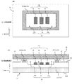
In the present embodiment, an example of wiring from the heater / thermal sensor wiring to the resistance readout circuit (comparator) in the semiconductor device 100 will be described.

図50(a)及び(b)は、本実施形態に係る半導体装置100の上面断面図及び側面断面図である。図50は、図31の半導体装置100に、ヒータ・熱センサ配線から比較器CMPまでの配線が追加されており、その他の構成は、図31と同様である。   50A and 50B are a top sectional view and a side sectional view of the semiconductor device 100 according to the present embodiment. In FIG. 50, wiring from the heater / thermal sensor wiring to the comparator CMP is added to the semiconductor device 100 of FIG. 31, and the other configurations are the same as those of FIG.

図50は、図31と同様に、ヒータ・熱センサ配線110を最上層より下層に形成した例である。なお、図28のように、ヒータ・熱センサ配線110を最上層に形成していてもよい。   FIG. 50 shows an example in which the heater / thermal sensor wiring 110 is formed below the uppermost layer, as in FIG. 31. As shown in FIG. 28, the heater / thermal sensor wiring 110 may be formed in the uppermost layer.

図50では、配線構造層Lは、図2と同様に、複数の層の配線構造層を含み、各配線構造層は、配線層及び層間絶縁膜を含んでいる。ここでは、配線構造層Lは、配線構造層L1〜L4を含んでいるものとして説明する。   In FIG. 50, the wiring structure layer L includes a plurality of wiring structure layers as in FIG. 2, and each wiring structure layer includes a wiring layer and an interlayer insulating film. Here, the wiring structure layer L will be described as including the wiring structure layers L1 to L4.

半導体装置100では、最上層に最上層配線構造20が形成され、その下層の配線構造層L4の配線層にヒータ・熱センサ配線110が形成されている。ヒータ・熱センサ配線110より下層の配線構造層L3の配線層に、配線ML210(ML210a、ML210b)が形成されている。配線ML210より下層の配線構造層L2の配線層に、配線ML200、配線ML220(ML220a、ML220b)が形成されている。配線ML200、配線ML220より下層の配線構造層L1及び半導体基板SUBに、抵抗読み出し回路である比較器CMPを構成するトランジスタM230(M230a,M230b)が形成されている。   In the semiconductor device 100, the uppermost wiring structure 20 is formed in the uppermost layer, and the heater / thermal sensor wiring 110 is formed in the wiring layer of the lower wiring structure layer L4. Wiring ML210 (ML210a, ML210b) is formed in the wiring layer of wiring structure layer L3 below heater / thermal sensor wiring 110. A wiring ML200 and a wiring ML220 (ML220a, ML220b) are formed in the wiring layer of the wiring structure layer L2 below the wiring ML210. Transistors M230 (M230a and M230b) constituting the comparator CMP which is a resistance read circuit are formed in the wiring ML200, the wiring structure layer L1 below the wiring ML220, and the semiconductor substrate SUB.

なお、ヒータ40の下方の配線ML200は、図25と同様に、ヒータ40からシリコン基板への熱伝導を遮断するための配線である。   Note that the wiring ML200 below the heater 40 is a wiring for cutting off heat conduction from the heater 40 to the silicon substrate, as in FIG.

熱センサ30、50は、図38に示したような配線構造となっており、熱センサ30、50の配線端部が、トレンチ配線(ビア)T210a、T210bを介して下層の配線ML210a、ML210bの一端に接続されている。ML210a、ML210bの他端は、トレンチ配線T220a、T220bを介して、さらに下層の配線ML220a、ML220bの一端に接続されている。ML220a、ML220bの他端は、トレンチ配線(コンタクト)T230a、T230bを介してトランジスタM230a、ML230bのゲート端子Gに接続されている。   The thermal sensors 30 and 50 have a wiring structure as shown in FIG. 38, and the wiring ends of the thermal sensors 30 and 50 are connected to the lower wirings ML210a and ML210b via the trench wirings (vias) T210a and T210b. Connected to one end. The other ends of ML210a and ML210b are connected to one end of lower layer wirings ML220a and ML220b via trench wirings T220a and T220b. The other ends of ML220a and ML220b are connected to gate terminals G of transistors M230a and ML230b via trench wirings (contacts) T230a and T230b.

抵抗読み出し回路(M230a,M230b)は、ヒータ40による熱の影響を避けるため、ヒータ40から離れた位置に配置される。そのため、配線ML210a、ML210bは、側面視でヒータ40から離れる方向に向かって形成されるとともに、上面視でヒータ40と反対側に折れ曲がって形成され、熱センサ30,50と読み出し回路とを接続している。   The resistance read circuits (M230a, M230b) are arranged at positions away from the heater 40 in order to avoid the influence of heat from the heater 40. For this reason, the wirings ML210a and ML210b are formed in a direction away from the heater 40 in a side view, and are bent in a direction opposite to the heater 40 in a top view, and connect the heat sensors 30 and 50 to the readout circuit. ing.

このように、熱センサと抵抗読み出し回路とを、熱センサよりも下層の配線を介して接続することにより、配線が空洞部に露出しないため、加速度センサの感度に影響を与えることなく、自由に配線を敷設することができる。   In this way, by connecting the thermal sensor and the resistance readout circuit via the lower layer wiring than the thermal sensor, the wiring is not exposed to the cavity, so it can be freely controlled without affecting the sensitivity of the acceleration sensor. Wiring can be laid.

実施の形態32
本実施形態では、半導体装置100における、ヒータ・熱センサ配線から抵抗読み出し回路(比較器)までの他の配線例について説明する。
Embodiment 32.
In the present embodiment, another wiring example from the heater / thermal sensor wiring to the resistance readout circuit (comparator) in the semiconductor device 100 will be described.

図51(a)及び(b)は、本実施形態に係る半導体装置100の上面断面図及び側面断面図である。図51では、図50の構成に対し、さらに、抵抗R231を追加した例である。抵抗R231は、図47の抵抗RI1に相当し、熱センサと比較器CMPとの間に接続される、熱伝導率の低い抵抗である。抵抗R231には、熱伝導率の小さい抵抗としてポリシリコンを用いるため、上層の配線層からトレンチ配線(コンタクト)を経由して下層のポリシリコン層まで下がって接続され、さらに、下層のポリシリコン層から上層の配線層に引き上げて接続される。   51A and 51B are a top sectional view and a side sectional view of the semiconductor device 100 according to the present embodiment. FIG. 51 is an example in which a resistor R231 is further added to the configuration of FIG. The resistor R231 corresponds to the resistor RI1 in FIG. 47, and is a resistor having low thermal conductivity that is connected between the thermal sensor and the comparator CMP. Since the polysilicon is used as the resistor having a low thermal conductivity, the resistor R231 is connected from the upper wiring layer to the lower polysilicon layer via the trench wiring (contact), and further connected to the lower polysilicon layer. To the upper wiring layer to be connected.

半導体装置100では、最上層に最上層配線構造20が形成され、その下層の配線構造層L4の配線層にヒータ・熱センサ配線110が形成されている。ヒータ・熱センサ配線110より下層の配線構造層L3の配線層に、配線ML210(ML210a、ML210b)、ML211(ML211a、ML211b)が形成されている。配線ML210より下層の配線構造層L2の配線層に、配線ML200、配線ML220(ML220a、ML220b)、配線ML221(ML221a、ML221b)、配線ML222(ML222a、ML222b)が形成されている。配線ML200、配線ML220より下層の配線構造層L1及び半導体基板SUBに、抵抗読み出し回路である比較器CMPを構成するトランジスタM230(M230a,M230b)が形成されている。   In the semiconductor device 100, the uppermost wiring structure 20 is formed in the uppermost layer, and the heater / thermal sensor wiring 110 is formed in the wiring layer of the lower wiring structure layer L4. Wiring ML210 (ML210a, ML210b) and ML211 (ML211a, ML211b) are formed in the wiring layer of the wiring structure layer L3 below the heater / thermal sensor wiring 110. A wiring ML200, a wiring ML220 (ML220a, ML220b), a wiring ML221 (ML221a, ML221b), and a wiring ML222 (ML222a, ML222b) are formed in the wiring layer of the wiring structure layer L2 below the wiring ML210. Transistors M230 (M230a and M230b) constituting the comparator CMP which is a resistance read circuit are formed in the wiring ML200, the wiring structure layer L1 below the wiring ML220, and the semiconductor substrate SUB.

熱センサ30、50は、その配線端部が、トレンチ配線T210a、T210bを介して下層の配線ML210a、ML210bの一端に接続されている。ML210aの他端は、トレンチ配線T221a、下層の配線ML221a、トレンチ配線T231aを介して、最下層の抵抗R231aの一端に接続されている。抵抗R231aの他端は、トレンチ配線T232a、上層の配線ML222a、トレンチ配線T232aを介して上層の配線ML211aの一端に接続されている。同様に、ML210bの他端は、トレンチ配線T221b、下層の配線ML221b、トレンチ配線T231bを介して、最下層の抵抗R231bの一端に接続されている。抵抗R231bの他端は、トレンチ配線T232b、上層の配線ML222b、トレンチ配線T232bを介して上層の配線ML211bの一端に接続されている。ML211a、ML211bの他端は、トレンチ配線T220a、T220bを介して、下層の配線ML220a、ML220bの一端に接続されている。配線ML220a、ML220bの他端は、トレンチ配線T230a、T230bを介してトランジスタM230a、M230bのゲート端子Gに接続されている。   The thermal sensor 30, 50 has its wiring end connected to one end of the lower wiring ML210a, ML210b via the trench wiring T210a, T210b. The other end of the ML 210a is connected to one end of the lowest-layer resistor R231a via the trench wiring T221a, the lower-layer wiring ML221a, and the trench wiring T231a. The other end of the resistor R231a is connected to one end of the upper wiring ML211a via the trench wiring T232a, the upper wiring ML222a, and the trench wiring T232a. Similarly, the other end of the ML 210b is connected to one end of the lowermost layer resistor R231b via the trench wiring T221b, the lower layer wiring ML221b, and the trench wiring T231b. The other end of the resistor R231b is connected to one end of the upper wiring ML211b via the trench wiring T232b, the upper wiring ML222b, and the trench wiring T232b. The other ends of ML211a and ML211b are connected to one ends of lower-layer wirings ML220a and ML220b via trench wirings T220a and T220b. The other ends of the wirings ML220a and ML220b are connected to the gate terminals G of the transistors M230a and M230b via the trench wirings T230a and T230b.

このように、熱センサ30,50と抵抗読み出し回路との間に、ポリシリコンによる熱伝導率の低い抵抗を接続することにより、熱センサ30,50の熱が逃げることを防ぎ、熱センサの感度を向上することができる。   In this way, by connecting a resistance having low thermal conductivity of polysilicon between the thermal sensors 30 and 50 and the resistance readout circuit, the heat of the thermal sensors 30 and 50 is prevented from escaping, and the sensitivity of the thermal sensor. Can be improved.

実施の形態33
本実施形態では、半導体装置100の熱検出回路の構成について説明する。半導体装置100では、例えば、図6等で示したような熱検出回路を用いることで、熱センサによる温度を検出することができる。
Embodiment 33.
In the present embodiment, the configuration of the heat detection circuit of the semiconductor device 100 will be described. In the semiconductor device 100, for example, by using a heat detection circuit as shown in FIG. 6 or the like, the temperature by the heat sensor can be detected.

しかし、熱センサの出力電圧には、半導体装置の素子のばらつきや周囲の環境等によりオフセットが生じる。特に、周囲の温度変化などの環境の変化により、出力電圧に生じるオフセットが時間と共に大きく変化するため、加速度を安定的に検出することが困難である。   However, an offset occurs in the output voltage of the thermal sensor due to variations in the elements of the semiconductor device, the surrounding environment, and the like. In particular, since the offset generated in the output voltage changes with time due to environmental changes such as ambient temperature changes, it is difficult to stably detect acceleration.

そこで、本実施形態では、熱センサのオフセットを動的に補正可能とするため、図52に示すような回路構成とする。   Therefore, in this embodiment, in order to dynamically correct the offset of the thermal sensor, a circuit configuration as shown in FIG. 52 is adopted.

図52は、本実施形態に係るヒータ駆動回路及び熱検出回路の回路構成例を示している。ヒータ駆動回路300は、図5のヒータ駆動回路に相当し、熱検出回路400は、図6の熱検出回路に相当する。   FIG. 52 shows a circuit configuration example of the heater drive circuit and the heat detection circuit according to the present embodiment. The heater drive circuit 300 corresponds to the heater drive circuit of FIG. 5, and the heat detection circuit 400 corresponds to the heat detection circuit of FIG.

ヒータ駆動回路300は、電源電位VDDと接地電位GND間に直列接続された抵抗R1及びスイッチ回路SW1を有する。スイッチ回路SW1のオン/オフは、コントローラ60によって制御される。抵抗R1はヒータ40に相当し、スイッチ回路SW1は図5のトランジスタM1に相当する。スイッチ回路SW1がオンのとき、抵抗R1に電流が流れてヒータ40が発熱し、スイッチ回路SW1がオフのときヒータ40は発熱しない。   The heater drive circuit 300 includes a resistor R1 and a switch circuit SW1 connected in series between the power supply potential VDD and the ground potential GND. On / off of the switch circuit SW1 is controlled by the controller 60. The resistor R1 corresponds to the heater 40, and the switch circuit SW1 corresponds to the transistor M1 in FIG. When the switch circuit SW1 is on, a current flows through the resistor R1 and the heater 40 generates heat. When the switch circuit SW1 is off, the heater 40 does not generate heat.

熱検出回路400は、熱センサ30もしくは50に相当する抵抗R2、抵抗R2の抵抗値を読み出す抵抗読み出し回路410、抵抗読み出し回路410の出力に対しオフセット補正を行うオフセット補正回路420を備えている。   The heat detection circuit 400 includes a resistor R2 corresponding to the heat sensor 30 or 50, a resistance reading circuit 410 that reads the resistance value of the resistor R2, and an offset correction circuit 420 that performs offset correction on the output of the resistance reading circuit 410.

抵抗読み出し回路410は、電流源CS1、抵抗R2、比較器CMP1を備えている。オフセット補正回路420は、スイッチ回路SW2、記憶素子MEM1、比較器CMP2を備えている。   The resistance read circuit 410 includes a current source CS1, a resistor R2, and a comparator CMP1. The offset correction circuit 420 includes a switch circuit SW2, a storage element MEM1, and a comparator CMP2.

電流源CS1及び抵抗R2は、電源電位VDDと接地電位GND間に直列に接続されており、電流源CS1及び抵抗R2の接点N1が、比較器CMP1の正端子(CIN)に入力される。比較器CMP1は、接点N1から読み出す電圧VN1と参照電圧VREFとを比較し、その差分値を増幅して読み出し電圧COUTを出力する。 The current source CS1 and the resistor R2 are connected in series between the power supply potential VDD and the ground potential GND, and the contact N1 of the current source CS1 and the resistor R2 is input to the positive terminal (C IN ) of the comparator CMP1. The comparator CMP1 compares the reference voltage VREF and the voltage V N1 to read from the contact N1, outputs the read voltage C OUT by amplifying a difference value.

スイッチ回路SW2は、比較器CMP1の出力端子と、比較器CMP2の正端子もしくは記憶素子MEM1とを接続する。スイッチ回路SW2のオン/オフは、コントローラ60によって制御される。スイッチ回路SW2がオンのとき、比較器CMP1の出力端子と、比較器CMP2の正端子とが接続され、スイッチ回路SW2がオフのとき、比較器CMP1の出力端子と記憶素子MEM1とが接続される。   The switch circuit SW2 connects the output terminal of the comparator CMP1 and the positive terminal of the comparator CMP2 or the storage element MEM1. On / off of the switch circuit SW2 is controlled by the controller 60. When the switch circuit SW2 is on, the output terminal of the comparator CMP1 and the positive terminal of the comparator CMP2 are connected. When the switch circuit SW2 is off, the output terminal of the comparator CMP1 and the storage element MEM1 are connected. .

記憶素子MEM1は、比較器CMP1と接続された場合に、比較器CMP1の出力電圧(読み出し電圧)COUTをオフセット電圧VOFFSETとして記憶する。比較器CMP2は、比較器CMP1と接続された場合に、比較器CMP1の出力電圧COUTと、記憶素子MEM1が記憶しているオフセット電圧VOFFSETとを比較し、その差分値を出力電圧VOUTとして出力する。 When connected to the comparator CMP1, the memory element MEM1 stores the output voltage (read voltage) C OUT of the comparator CMP1 as an offset voltage V OFFSET . When connected to the comparator CMP1, the comparator CMP2 compares the output voltage C OUT of the comparator CMP1 with the offset voltage V OFFSET stored in the storage element MEM1, and compares the difference value with the output voltage V OUT. Output as.

コントローラ60によって、ヒータ駆動回路300のスイッチ回路SW1のオン/オフと、熱検出回路400のスイッチ回路SW2のオン/オフとが同期して切り替えられる。すなわち、ヒータ40のオン/オフのタイミングと、熱センサによる熱検出の出力もしくはオフセット記憶のタイミングを同期させる。   The controller 60 switches on / off of the switch circuit SW1 of the heater drive circuit 300 and on / off of the switch circuit SW2 of the heat detection circuit 400 in synchronization. That is, the heater 40 on / off timing is synchronized with the heat detection output or offset storage timing of the thermal sensor.

スイッチ回路SW1及びSW2をオフすることにより、ヒータがオフの時、抵抗(センサ抵抗)R2による出力電圧COUTが、オフセット値VOFFSETとして記憶素子MEM1に記憶される。スイッチ回路SW1及びSW2をオンすることにより、ヒータがオンの時、抵抗R2による電圧COUTからオフセット値VOFFSETを差し引いた電圧を、出力電圧VOUTとして出力する。 By turning off the switch circuits SW1 and SW2, when the heater is turned off, the output voltage C OUT by the resistor (sensor resistance) R2 is stored in the memory element MEM1 as the offset value V OFFSET . By turning on the switch circuits SW1 and SW2, when the heater is on, a voltage obtained by subtracting the offset value V OFFSET from the voltage C OUT by the resistor R2 is output as the output voltage VOUT .

図53は、ヒータ40がオンの時とオフの時のヒータ40、熱センサ30、熱センサ50近傍の温度分布を示している。   FIG. 53 shows the temperature distribution in the vicinity of the heater 40, the thermal sensor 30, and the thermal sensor 50 when the heater 40 is on and off.

ヒータ40がオンの場合、図53(a)に示すように、半導体装置100の静止時と移動時とで温度分布が異なる。すなわち、半導体装置100が静止していると、温度分布は、ヒータ40を中心として熱センサ30側と熱センサ50側とで左右対称である。一方、半導体装置100が移動すると、ガスの流れが発生するため、温度分布は、ヒータ40を中心として熱センサ30側と熱センサ50側とで左右非対称となる。このため、熱センサ30と熱センサ50付近の温度差によって、加速度が検出できる。   When the heater 40 is on, the temperature distribution differs between when the semiconductor device 100 is stationary and when it is moved, as shown in FIG. That is, when the semiconductor device 100 is stationary, the temperature distribution is symmetrical between the heat sensor 30 side and the heat sensor 50 side with respect to the heater 40. On the other hand, when the semiconductor device 100 moves, a gas flow is generated. Therefore, the temperature distribution is asymmetrical between the heat sensor 30 side and the heat sensor 50 side with respect to the heater 40. For this reason, acceleration can be detected by a temperature difference between the thermal sensor 30 and the thermal sensor 50.

これに対して、ヒータ40がオフの場合、図53(b)に示すように、半導体装置100の静止時と移動時とで温度分布は同じである。すなわち、ヒータ40が発熱せずガスの温度が一定のため、半導体装置100が静止していても動作していても、温度分布は変化しない。このため、熱センサ30と熱センサ50付近の温度差が発生しないため、加速度は検出されない。したがって、ヒータがオフのときの熱センサの温度差は、加速度を含まないオフセット値となる。つまり、オフセット値は、ヒータ40による発熱の影響を受けない状態の熱センサの出力である。   On the other hand, when the heater 40 is off, the temperature distribution is the same when the semiconductor device 100 is stationary and when it is moved, as shown in FIG. That is, since the heater 40 does not generate heat and the gas temperature is constant, the temperature distribution does not change even if the semiconductor device 100 is stationary or operating. For this reason, since a temperature difference between the thermal sensor 30 and the thermal sensor 50 does not occur, acceleration is not detected. Therefore, the temperature difference of the thermal sensor when the heater is off is an offset value that does not include acceleration. That is, the offset value is the output of the heat sensor in a state where it is not affected by the heat generated by the heater 40.

本実施形態では、ヒータ40をオフにした時に、このオフセット値を、図52の記憶素子MEM1に記憶させ、ヒータ40をオンにした時に、比較器CMP2でオフセット値を差し引くことにより、オフセット補正を行う。これにより、精度よく安定して加速度を検出することができる。   In this embodiment, when the heater 40 is turned off, this offset value is stored in the memory element MEM1 of FIG. 52, and when the heater 40 is turned on, the offset value is subtracted by the comparator CMP2, thereby correcting the offset. Do. As a result, the acceleration can be detected accurately and stably.

また、ヒータを間欠的に動作させ、熱センサのオフセットの記憶と、熱センサの検出値のオフセット補正とを繰り返すことで、特性変動をリアルタイムに補正することができる。   Further, the characteristic variation can be corrected in real time by intermittently operating the heater and repeating the storage of the offset of the thermal sensor and the offset correction of the detection value of the thermal sensor.

実施の形態34
本実施形態では、図52で示した熱検出回路を用いた半導体装置100の実際の測定結果について説明する。
Embodiment 34.
In this embodiment, an actual measurement result of the semiconductor device 100 using the heat detection circuit shown in FIG. 52 will be described.

図54は、加速度センサである半導体装置100による加速度の検出動作を測定するための測定システムの構成を示している。ここでは、本発明の半導体装置100の出力を、他の加速度センサの出力と比較することで、検出動作を確認する。このため、比較対象としてリファレンスとなる加速度センサ501の出力も同時に測定する。加速度センサ501は、検出する加速度に応じた信号を出力する一般的な加速度センサである。   FIG. 54 shows a configuration of a measurement system for measuring an acceleration detection operation by the semiconductor device 100 which is an acceleration sensor. Here, the detection operation is confirmed by comparing the output of the semiconductor device 100 of the present invention with the output of another acceleration sensor. For this reason, the output of the acceleration sensor 501 serving as a reference as a comparison target is also measured simultaneously. The acceleration sensor 501 is a general acceleration sensor that outputs a signal corresponding to the detected acceleration.

図54に示すように、本発明の半導体装置100と加速度センサ501を同じ評価ボード502上に実装し、この評価ボード502に水平方向の振動を加える。   As shown in FIG. 54, the semiconductor device 100 of the present invention and the acceleration sensor 501 are mounted on the same evaluation board 502, and a horizontal vibration is applied to the evaluation board 502.

評価ボード502上では、熱センサの抵抗値を読み出す抵抗読み出し回路410が半導体装置100に接続される。上述のように、抵抗読み出し回路410は、半導体装置100の内部に形成することもできるし、図54のように半導体装置100の外部に設けることもできる。   On the evaluation board 502, a resistance read circuit 410 that reads the resistance value of the thermal sensor is connected to the semiconductor device 100. As described above, the resistance readout circuit 410 can be formed inside the semiconductor device 100, or can be provided outside the semiconductor device 100 as shown in FIG.

図55は、図54の読み出し回路410の回路構成を示している。センサ抵抗Rs1及びRs2は、半導体装置100の熱センサ30,50に相当する抵抗である。センサ抵抗Rs1及びRs2の両端の計4端子を、読み出し回路410に接続する。   FIG. 55 shows a circuit configuration of the readout circuit 410 of FIG. The sensor resistances Rs1 and Rs2 are resistances corresponding to the thermal sensors 30 and 50 of the semiconductor device 100. A total of four terminals at both ends of the sensor resistors Rs 1 and Rs 2 are connected to the readout circuit 410.

読み出し回路410は、抵抗Rr1〜Rr4、オペアンプ411、帰還抵抗Rfを備えている。抵抗Rr1〜Rr4は、抵抗Rr4、Rr3、Rr2、Rr1の順に、電源電位VDDと接地電位GND間に直列接続されている。   The read circuit 410 includes resistors Rr1 to Rr4, an operational amplifier 411, and a feedback resistor Rf. The resistors Rr1 to Rr4 are connected in series between the power supply potential VDD and the ground potential GND in the order of the resistors Rr4, Rr3, Rr2, and Rr1.

抵抗Rr4と抵抗Rr3の間の接点が、抵抗Rs1の一端に接続され、この接点電圧V1が抵抗Rs1に与えられる。抵抗Rr2と抵抗Rr1の間の接点が、抵抗Rs2の一端に接続され、この接点電圧V2が抵抗Rs2に与えられる。   A contact point between the resistor Rr4 and the resistor Rr3 is connected to one end of the resistor Rs1, and the contact voltage V1 is given to the resistor Rs1. A contact between the resistor Rr2 and the resistor Rr1 is connected to one end of the resistor Rs2, and the contact voltage V2 is applied to the resistor Rs2.

抵抗Rr3と抵抗Rr2の間の接点(電圧Vm)が、オペアンプ411の正端子に接続され、この接点電圧Vmがオペアンプ411に与えられる。抵抗Rs1の他端と抵抗Rs2の他端とが共通接続され、この接点がオペアンプ411の負端子に接続され、この接点電圧Vsがオペアンプ411に与えられる。さらに、オペアンプ411の出力端子が、帰還抵抗Rfを介して負端子にフィードバック接続される。   A contact (voltage Vm) between the resistor Rr3 and the resistor Rr2 is connected to the positive terminal of the operational amplifier 411, and this contact voltage Vm is applied to the operational amplifier 411. The other end of the resistor Rs1 and the other end of the resistor Rs2 are connected in common, the contact is connected to the negative terminal of the operational amplifier 411, and the contact voltage Vs is applied to the operational amplifier 411. Further, the output terminal of the operational amplifier 411 is feedback-connected to the negative terminal via the feedback resistor Rf.

読み出し回路410は、抵抗Rs1と抵抗Rs2の抵抗値の変化によって発生した電圧Vsを、オペアンプ411が増幅し、検出電圧(読み出し電圧)Vsensとして出力する。ここでは、各抵抗の抵抗値を、抵抗Rr1=Rr4=1kΩ、Rr2=Rr3=100Ω、Rf=10kΩとし、VDD=5Vを供給して読み出し回路410を動作させ、測定を行った。   In the read circuit 410, the operational amplifier 411 amplifies the voltage Vs generated by the change in the resistance values of the resistors Rs1 and Rs2, and outputs the amplified voltage Vsens as a detection voltage (read voltage) Vsens. Here, the resistance values of the resistors were set to resistors Rr1 = Rr4 = 1 kΩ, Rr2 = Rr3 = 100Ω, Rf = 10 kΩ, VDD = 5 V was supplied to operate the reading circuit 410, and measurement was performed.

さらに、図54に示すように、半導体装置100のヒータ40にはパルスジェネレータ507を接続する。パルスジェネレータ507には、Agilent社の33250Aを用いた。パルスジェネレータ507から出力されるパルス信号により、間欠的にヒータ40のオンオフを繰り返す。ヒータ40のオンオフの周波数は4Hzとした。また、パルスジェネレータ507の発生するパルス信号は、パルス測定用のデジタルマルチメータ503で測定する。   Further, as shown in FIG. 54, a pulse generator 507 is connected to the heater 40 of the semiconductor device 100. For the pulse generator 507, Agilent 33250A was used. The heater 40 is turned on and off intermittently by the pulse signal output from the pulse generator 507. The on / off frequency of the heater 40 was 4 Hz. The pulse signal generated by the pulse generator 507 is measured by a digital multimeter 503 for pulse measurement.

そして、半導体装置100に接続される読み出し回路410の出力電圧をTEG(Test Element Group)測定用のデジタルマルチメータ504で測定し、同時に加速度センサ501の出力電圧をリファレンス測定用のデジタルマルチメータ505で測定する。デジタルマルチメータ503〜505には、Agilent社の34410Aを用いた。デジタルマルチメータ503〜505の測定結果は、GPIB(General Purpose Interface Bus)を介して、制御用パソコン506に出力する。   Then, the output voltage of the readout circuit 410 connected to the semiconductor device 100 is measured with a digital multimeter 504 for TEG (Test Element Group) measurement, and at the same time, the output voltage of the acceleration sensor 501 is measured with a digital multimeter 505 for reference measurement. taking measurement. Agilent's 34410A was used for the digital multimeters 503 to 505. The measurement results of the digital multimeters 503 to 505 are output to the control personal computer 506 via GPIB (General Purpose Interface Bus).

制御用パソコン506は、デジタルマルチメータ503で測定されたヒータのオンオフのパルスと、デジタルマルチメータ504で測定された読み出し回路410の電圧により、検出された加速度を求める。ヒータがオフの期間に、読み出し回路410の出力電圧の測定値の平均値を計算して、求めた平均値をオフセット値として記憶する。ヒータがオンの期間に、読み出し回路410の出力電圧の測定値から、記憶してあるオフセット値を差し引いてオフセット補正し、オフセット補正後の電圧を検出した加速度とする。   The control personal computer 506 obtains the detected acceleration based on the heater on / off pulse measured by the digital multimeter 503 and the voltage of the readout circuit 410 measured by the digital multimeter 504. While the heater is off, the average value of the measured values of the output voltage of the readout circuit 410 is calculated, and the obtained average value is stored as an offset value. While the heater is on, offset correction is performed by subtracting the stored offset value from the measured value of the output voltage of the readout circuit 410, and the offset-corrected voltage is used as the detected acceleration.

すなわち、この測定例では、制御用パソコン506がオフセット補正を行っており、図52で示したオフセット補正回路420は、制御用パソコン506に相当する。   That is, in this measurement example, the control personal computer 506 performs offset correction, and the offset correction circuit 420 shown in FIG. 52 corresponds to the control personal computer 506.

なお、加速度センサ501の出力信号は、デジタルマルチメータ505で測定され、制御用パソコン506が、この測定結果を演算処理し、検出された加速度を求める。   The output signal of the acceleration sensor 501 is measured by the digital multimeter 505, and the control personal computer 506 computes the measurement result to obtain the detected acceleration.

図56は、図54の測定システムの測定結果を示している。図56では、横軸は時間となっており、時間的に変化する加速度に対する半導体装置100及び加速度センサ501の応答を示している。横軸に対し、図面左側の縦軸は読み出し回路410が出力する出力電圧の目盛りであり、図面右側の縦軸は加速度センサ501が検出する加速度の目盛りである。   FIG. 56 shows the measurement results of the measurement system of FIG. In FIG. 56, the horizontal axis represents time, and shows the response of the semiconductor device 100 and the acceleration sensor 501 to the acceleration that changes with time. With respect to the horizontal axis, the vertical axis on the left side of the drawing is a scale of the output voltage output from the readout circuit 410, and the vertical axis on the right side of the drawing is a scale of the acceleration detected by the acceleration sensor 501.

点線の折れ線(a)は、リファレンスとなる加速度センサ501により検出された加速度であり、これが評価ボード502に加えられた加速度である。一点鎖線の折れ線(b)は、読み出し回路410から出力されたオフセット補正前の本発明の出力電圧である。図55のVSENS(図52のCOUT)に相当する。実線の折れ線(c)は、折れ線(b)の出力電圧に対しオフセット補正したオフセット補正後の本発明の出力電圧である。図52のVOUTに相当する。 A dotted broken line (a) is an acceleration detected by the acceleration sensor 501 serving as a reference, and this is an acceleration applied to the evaluation board 502. The broken line (b) of the alternate long and short dash line is the output voltage of the present invention before offset correction output from the readout circuit 410. This corresponds to V SENS in FIG. 55 (C OUT in FIG. 52). The solid broken line (c) is the output voltage of the present invention after the offset correction in which the offset voltage is corrected with respect to the output voltage of the broken line (b). This corresponds to VOUT in FIG.

リファレンスである折れ線(a)と、本発明の折れ線(b)とを比較すると、折れ線(b)に示されるように、オフセット補正前は、オフセット量の時間変化によって出力電圧のドリフトが起こり、加速度センサ501の検出する加速度との差が大きい。これに対し、本発明の折れ線(c)に示されるように、オフセット補正後は、オフセット補正によってドリフトが解消し、加速度センサ501の検出する加速度に近い出力波形が得られていることが分かる。したがって、図52のようなオフセット補正回路によりリアルタイムに補正を行うことで、図56に示すように、通常の加速度センサと同様に、加速度検出動作を行うことができた。   When the broken line (a) as a reference is compared with the broken line (b) of the present invention, as shown by the broken line (b), the drift of the output voltage occurs due to the time change of the offset amount before the offset correction, and the acceleration The difference from the acceleration detected by the sensor 501 is large. On the other hand, as indicated by the broken line (c) of the present invention, it can be seen that after the offset correction, the drift is eliminated by the offset correction, and an output waveform close to the acceleration detected by the acceleration sensor 501 is obtained. Therefore, by performing the correction in real time by the offset correction circuit as shown in FIG. 52, as shown in FIG. 56, the acceleration detection operation can be performed in the same manner as a normal acceleration sensor.

実施の形態35
本実施形態では、半導体装置100のオフセット補正回路をアナログ回路により構成した例について説明する。
Embodiment 35.
In the present embodiment, an example in which the offset correction circuit of the semiconductor device 100 is configured by an analog circuit will be described.

図57は、本実施形態に係る半導体装置100における熱検出回路の回路構成例を示している。図57は、図52で示した記憶素子MEM1の具体的な回路構成を示しており、その他の構成は図52と同様である。   FIG. 57 shows a circuit configuration example of the heat detection circuit in the semiconductor device 100 according to the present embodiment. FIG. 57 shows a specific circuit configuration of the memory element MEM1 shown in FIG. 52, and the other configurations are the same as those in FIG.

図57では記憶素子MEM1として、容量Cref及び入力抵抗Rrefを用いる。入力抵抗Rrefの一端が、スイッチ回路SW2を介して比較器CMP1の出力端子に接続され、入力抵抗Rrefの他端が、容量Crefの一端及び比較器CMP2の負端子に接続される。容量Crefの他端が接地電位GNDに接続される。   In FIG. 57, a capacitor Cref and an input resistor Rref are used as the memory element MEM1. One end of the input resistor Rref is connected to the output terminal of the comparator CMP1 via the switch circuit SW2, and the other end of the input resistor Rref is connected to one end of the capacitor Cref and the negative terminal of the comparator CMP2. The other end of the capacitor Cref is connected to the ground potential GND.

容量Crefと入力抵抗Rrefは、ローバスフィルタを構成する。したがって、出力電圧COUTのオフセット値のうち、高周波成分を除去し低周波成分のみを取り出して、容量Crefに記憶する。 The capacitor Cref and the input resistance Rref constitute a low-pass filter. Therefore, the high frequency component is removed from the offset value of the output voltage C OUT and only the low frequency component is extracted and stored in the capacitor Cref.

このように、本実施形態では、図52と同様の構成により、リアルタイムなオフセット補正が可能である。さらに、記憶素子MEM1を、容量Crefと入力抵抗Rrefで構成することにより、簡易に回路を構成できるとともに、ローパスフィルタとして出力電圧COUTに含まれる高周波ノイズの影響を防ぐことができる。 Thus, in the present embodiment, real-time offset correction is possible with the same configuration as in FIG. Further, the storage element MEM1, by configuring an input resistor Rref and capacitor Cref, it is possible to configure the circuit simply, it is possible to prevent the influence of high frequency noise included in the output voltage C OUT as a low pass filter.

実施の形態36
本実施形態では、半導体装置100のオフセット補正回路をデジタル回路により構成した例について説明する。
Embodiment 36.
In the present embodiment, an example in which the offset correction circuit of the semiconductor device 100 is configured by a digital circuit will be described.

図58は、本実施形態に係る半導体装置100における熱検出回路の回路構成例を示している。図58は、図52で示したオフセット補正回路420をデジタル回路で構成しており、その他の構成は図52と同様である。   FIG. 58 shows a circuit configuration example of the heat detection circuit in the semiconductor device 100 according to the present embodiment. 58, the offset correction circuit 420 shown in FIG. 52 is configured by a digital circuit, and other configurations are the same as those in FIG.

図58では、オフセット補正回路420は、AD変換器ADC1、記憶素子MEM1、デジタルフィルタDF1、減算器SU1を有している。   In FIG. 58, the offset correction circuit 420 includes an AD converter ADC1, a storage element MEM1, a digital filter DF1, and a subtractor SU1.

AD変換器ADC1は、比較器CMP1の出力信号をデジタル信号に変換し、減算器SU1もしくは記憶素子MEM1へ出力する。   The AD converter ADC1 converts the output signal of the comparator CMP1 into a digital signal and outputs it to the subtractor SU1 or the storage element MEM1.

ヒータがオフの時、このデジタル信号を記憶素子MEMに記憶させる。デジタルフィルタDF1は、記憶素子MEMが記憶したデジタル信号のうち、高周波成分を除去し低周波成分だけをオフセット値として減算器SU1へ出力する。ヒータがオンの時、減算器SU1は、AD変換器ADC1の出力するデジタル信号から、記憶素子MEM1で記憶したオフセット値を減算し、減算結果をデジタル信号の出力DOUTとして出力する。 When the heater is off, this digital signal is stored in the storage element MEM. The digital filter DF1 removes the high frequency component from the digital signal stored in the storage element MEM and outputs only the low frequency component as an offset value to the subtracter SU1. When the heater is on, the subtractor SU1 subtracts the offset value stored in the storage element MEM1 from the digital signal output from the AD converter ADC1, and outputs the subtraction result as the digital signal output DOUT .

このように、本実施形態では、図52と同様の構成により、リアルタイムなオフセット補正が可能である。さらに、オフセット補正回路をデジタル回路により構成することで、デジタル信号処理により実現できるため、マイクロコンピュータ等を用いて構成することができる。マイクロコンピュータ等ではソフトウェアによる演算処理を行うため、アナログ回路を形成することなく、実現が可能である。   Thus, in the present embodiment, real-time offset correction is possible with the same configuration as in FIG. Furthermore, since the offset correction circuit is configured by a digital circuit and can be realized by digital signal processing, it can be configured by using a microcomputer or the like. Since a microcomputer or the like performs calculation processing by software, it can be realized without forming an analog circuit.

実施の形態37
本実施形態では、半導体装置100の抵抗読み出し回路で用いられる比較器の構成例について説明する。図46,47,49,52,55等で示したように半導体装置100の抵抗読み出し回路410は比較器CMP(もしくはCMP1)を有している。この比較器CMPには、例えば通常のオペアンプを使用することができる。
Embodiment 37.
In this embodiment, a configuration example of a comparator used in the resistance read circuit of the semiconductor device 100 will be described. As shown in FIGS. 46, 47, 49, 52, 55, etc., the resistance read circuit 410 of the semiconductor device 100 has a comparator CMP (or CMP1). For example, a normal operational amplifier can be used for the comparator CMP.

本実施形態では、比較器CMPとして、オペアンプの代わりにチョッパ式アンプを使用する。図59は、本実施形態の比較器CMPの構成を示している。図59に示すように、比較器CMPは、チョッパ式アンプにより構成されており、2つの切り替えスイッチ601,603、差動アンプ602、低域通過フィルタ604を有している。切り替えスイッチ601、差動アンプ602、切り替えスイッチ603、低域通過フィルタ604の順に直列に接続されている。切り替えスイッチ601,603は、2入力2出力のスイッチ回路である。切り替えスイッチ601と切り替えスイッチ603は同一のクロック信号(切替信号)で同時に切り替えが行われる。   In this embodiment, a chopper amplifier is used as the comparator CMP instead of the operational amplifier. FIG. 59 shows a configuration of the comparator CMP of the present embodiment. As shown in FIG. 59, the comparator CMP is configured by a chopper amplifier, and includes two changeover switches 601, 603, a differential amplifier 602, and a low-pass filter 604. A changeover switch 601, a differential amplifier 602, a changeover switch 603, and a low-pass filter 604 are connected in series in this order. The changeover switches 601 and 603 are 2-input 2-output switch circuits. The changeover switch 601 and the changeover switch 603 are simultaneously switched by the same clock signal (switching signal).

切り替えスイッチ601は、参照電圧VREFとCIN(比較器CMPの入力)のそれぞれを、差動アンプの負入力AINBと正入力AINTとのいずれかに接続する。差動アンプ602は、切り替えスイッチ601から負入力AINB、正入力AINTに入力される信号を差動増幅し、増幅された信号を負出力AOUB、正出力AOUTに出力する。切り替えスイッチ603は、差動アンプ602の負出力AOUBと正出力AOUTのそれぞれを、低域通過フィルタ604の負入力FINBと正入力FINTとのいずれかに接続する。低域通過フィルタ604は、切り替えスイッチ603から負入力FINB、正入力FINTに入力される信号から高周波成分を除去し、低周波成分の信号をCOUT(比較器CMPの出力)に出力する。 The changeover switch 601 connects each of the reference voltages VREF and C IN (input of the comparator CMP) to either the negative input A INB or the positive input A INT of the differential amplifier. The differential amplifier 602 differentially amplifies the signals input from the changeover switch 601 to the negative input A INB and the positive input A INT and outputs the amplified signals to the negative output A OUB and the positive output A OUT . The changeover switch 603 connects each of the negative output A OUB and the positive output A OUT of the differential amplifier 602 to either the negative input F INB or the positive input F INT of the low-pass filter 604. The low-pass filter 604 removes a high frequency component from the signal input to the negative input F INB and the positive input F INT from the changeover switch 603, and outputs a low frequency component signal to C OUT (output of the comparator CMP). .

図60は、図59で示したチョッパ式アンプで構成された比較器CMPの動作を示している。チョッパ式アンプは切り替えスイッチ601,603の状態により、正相と逆相の2つの状態を有している。切り替えスイッチ601,603に供給されるクロック信号により、正相と逆相とを交互に繰り返す。   FIG. 60 shows the operation of the comparator CMP composed of the chopper type amplifier shown in FIG. The chopper type amplifier has two states of a normal phase and a reverse phase depending on the state of the changeover switches 601 and 603. By the clock signal supplied to the changeover switches 601 and 603, the normal phase and the reverse phase are alternately repeated.

図60(a)は正相の場合の信号の流れを示している。正相の場合、切り替えスイッチ601は、VREFとAINBとを接続し、CINとAINTとを接続する。そして、切り替えスイッチ603は、AOUBとFINBとを接続し、AOUTとFINTとを接続する。したがって、正相の場合、CINから入力された信号は、実線矢印610に示すように、CIN−AINT−AOUT−FINT−COUTと伝わる。 FIG. 60A shows the signal flow in the case of the positive phase. In the case of the positive phase, the changeover switch 601 connects VREF and A INB and connects C IN and A INT . The changeover switch 603 connects A OUB and F INB and connects A OUT and F INT . Therefore, in the case of the positive phase, the signal input from C IN is transmitted as C IN −A INT −A OUT −F INT −C OUT as indicated by a solid line arrow 610.

また、図60(b)は逆相の場合の信号の流れを示している。逆相の場合、切り替えスイッチ601は、VREFとAINTとを接続し、CINとAINBとを接続する。そして、切り替えスイッチ603は、AOUBとFINTとを接続し、AOUTとFINBとを接続する。したがって、逆相の場合、CINから入力された信号は、点線矢印611に示すように、CIN−AINB−AOUB−FINT−COUTと伝わる。つまり、正相と逆相ではCINから入力された信号が、差動アンプ602の正入力AINTと負入力AINBとのいずれを通るのかが異なる。 FIG. 60B shows a signal flow in the case of reverse phase. In the case of reverse phase, the changeover switch 601 connects VREF and A INT , and connects C IN and A INB . The changeover switch 603 connects A OUB and F INT and connects A OUT and F INB . Therefore, if the reverse phase, the signal inputted from C IN, as shown in a dotted arrow 611, transmitted and C IN -A INB -A OUB -F INT -C OUT. In other words, the positive phase and the reverse phase differ depending on whether the signal input from C IN passes through the positive input A INT or the negative input A INB of the differential amplifier 602.

ここで、差動アンプ602が素子ばらつきなどの影響で入力にオフセット電圧ΔVを持ち、差動アンプ602のゲインをGAMPとする。そうすると、CINに信号が全く入力されていない、つまり、CIN=VREFとしたとき、チョッパ式アンプが正相の期間では、差動アンプ602の出力にはΔV×GAMPの電圧が出力され、チョッパ式アンプが逆相の期間では、差動アンプ602の出力には−ΔV×GAMPの電圧がオフセットとして出力される。 Here, it is assumed that the differential amplifier 602 has an offset voltage ΔV at the input due to element variations and the like, and the gain of the differential amplifier 602 is G AMP . Then, the signal is not at all input to the C IN, that is, when the C IN = VREF, the chopper-type amplifier in a period of positive phase, the voltage of the [Delta] V × G AMP is output to the output of the differential amplifier 602 When the chopper type amplifier is in the opposite phase, a voltage of −ΔV × G AMP is output as an offset to the output of the differential amplifier 602.

図61、図59、60のFINTとCOUTでの信号波形を模式的に表したものである。チョッパ式アンプが正相と逆相を繰り返すことに応じて、FINTでの信号は、ΔV×GAMPと−ΔV×GAMPを交互に繰り返す。このFINTの信号が、低域通過フィルタ604を通ると、繰り返されている信号は平均化されて、ΔV×GAMPと−ΔV×GAMPの平均値、つまり0VがCOUTに出力される。 61 schematically illustrates signal waveforms at F INT and C OUT in FIGS. 61, 59, and 60. FIG. As the chopper type amplifier repeats the normal phase and the reverse phase, the signal at F INT repeats ΔV × G AMP and −ΔV × G AMP alternately. When the F INT signal passes through the low-pass filter 604, the repeated signal is averaged, and an average value of ΔV × G AMP and −ΔV × G AMP , that is, 0 V is output to C OUT. .

このように、比較器CMPをチョッパ式アンプにより構成することにより、差動アンプのオフセットの影響が出力に現れないので、差動アンプのオフセット電圧よりも小さい微小な信号を正確に増幅することができる。したがって、半導体装置100の抵抗読み出し回路にこの比較器CMPを用いることで、熱センサの温度を正確に検出することができる。   Thus, by configuring the comparator CMP with a chopper amplifier, the influence of the offset of the differential amplifier does not appear in the output, so that a minute signal smaller than the offset voltage of the differential amplifier can be accurately amplified. it can. Therefore, by using the comparator CMP in the resistance read circuit of the semiconductor device 100, the temperature of the thermal sensor can be accurately detected.

100 半導体装置

10 積層体
20 配線層
20a 壁配線
20b 壁配線
21 保護層
22 ガス流路
25 板状部材
30 熱センサ
31 ランド
32 ランド
33 パターン配線部
40 ヒータ
41 ランド
42 ランド
43 パターン配線部
50 熱センサ
51 ランド
52 ランド
53 パターン配線部
60 コントローラ
61 演算処理部

SUB 半導体基板
L1-L3 配線構造層
R30-R50 パターニング領域

23 キャビティ
24 空洞部
110 ヒータ・熱センサ配線
110a ミアンダ配線部
110b 戻り配線部
111 カバー膜
120−122 配線パターン
130−131 ダミーメタル
300 ヒータ駆動回路
400 熱検出回路
410 抵抗読み出し回路
420 オフセット補正回路
100 Semiconductor device

DESCRIPTION OF SYMBOLS 10 Laminate 20 Wiring layer 20a Wall wiring 20b Wall wiring 21 Protective layer 22 Gas flow path 25 Plate-shaped member 30 Thermal sensor 31 Land 32 Land 33 Pattern wiring part 40 Heater 41 Land 42 Land 43 Pattern wiring part 50 Thermal sensor 51 Land 52 Land 53 Pattern wiring unit 60 Controller 61 Arithmetic processing unit

SUB semiconductor substrate L1-L3 wiring structure layer R30-R50 patterning region

23 Cavity 24 Cavity 110 Heater / thermal sensor wiring 110a Meander wiring 110b Return wiring 111 Cover film 120-122 Wiring pattern 130-131 Dummy metal 300 Heater drive circuit 400 Heat detection circuit 410 Resistance readout circuit 420 Offset correction circuit

Claims (29)

凹状のガス流路が設けられた積層体と、
前記積層体に対して設けられると共に、前記ガス流路の底面にて露出する発熱部と、
前記積層体に対して設けられると共に、前記ガス流路の前記底面にて露出し、かつ前記ガス流路の延在方向において前記発熱部を挟み込むように配置された複数の感温部と、
を備える、半導体装置。
A laminate provided with a concave gas flow path;
A heat generating portion that is provided on the laminate and exposed at a bottom surface of the gas flow path;
A plurality of temperature sensing parts provided to the laminate, exposed at the bottom surface of the gas flow path, and arranged to sandwich the heat generating part in the extending direction of the gas flow path;
A semiconductor device comprising:
前記積層体は、
半導体基板と、
前記半導体基板上に設けられ、絶縁層と配線層とを含む配線構造層と、
前記配線構造層上に設けられ、前記ガス流路が設けられた最上層配線構造と、
を備え、
前記発熱部は、前記配線構造層に含まれる前記絶縁層を介して、前記半導体基板に対して熱分離されていることを特徴とする請求項1に記載の半導体装置。
The laminate is
A semiconductor substrate;
A wiring structure layer provided on the semiconductor substrate and including an insulating layer and a wiring layer;
An uppermost wiring structure provided on the wiring structure layer and provided with the gas flow path;
With
The semiconductor device according to claim 1, wherein the heat generating part is thermally isolated from the semiconductor substrate via the insulating layer included in the wiring structure layer.
前記凹状のガス流路の周囲には、配線構造の凸形状で形成された壁配線を持つことを特徴とした請求項1又は2に記載の半導体装置。   3. The semiconductor device according to claim 1, wherein a wall wiring formed in a convex shape of a wiring structure is provided around the concave gas flow path. 前記発熱部及び前記感温部は、前記ガス流路の前記底面においてパターニングされた導電線を含み、
前記ガス流路を上面視すると、前記ガス流路には、前記導電線のパターニングによって形成された複数のパターニング領域が設けられていることを特徴とする請求項1乃至3のいずれか一項に記載の半導体装置。
The heat generating part and the temperature sensing part include a conductive wire patterned on the bottom surface of the gas flow path,
When the gas flow path is viewed from above, the gas flow path is provided with a plurality of patterning regions formed by patterning the conductive lines. The semiconductor device described.
前記発熱部及び前記感温部は、アルミニウム、銅、タングステン、金、白金、バナジウム、チタン、鉄、ニッケルもしくはこれらの合金や酸化物もしくは窒化物で形成されていることを特徴とする請求項1乃至4のいずれか一項に記載の半導体装置。   2. The heat generating part and the temperature sensing part are formed of aluminum, copper, tungsten, gold, platinum, vanadium, titanium, iron, nickel, or an alloy, oxide or nitride thereof. The semiconductor device as described in any one of thru | or 4. 前記発熱部及び前記感温部は、前記ガス流路の前記底面においてパターニングされた導電線を含み、
前記ガス流路を上面視すると、前記ガス流路には、前記導電線のパターニングによって形成された少なくとも1つの発熱部と少なくとも2つの感温部を有することを特徴とする請求項1乃至5のいずれか一項に記載の半導体装置。
The heat generating part and the temperature sensing part include a conductive wire patterned on the bottom surface of the gas flow path,
6. The gas flow path according to claim 1, wherein the gas flow path has at least one heat generating part and at least two temperature sensitive parts formed by patterning the conductive wire when viewed from above. The semiconductor device as described in any one.
前記発熱部及び前記感温部は、前記ガス流路の前記底面においてパターニングされた導電線を含み、
前記ガス流路を上面視すると、前記ガス流路には、前記導電線のパターニングによって形成された少なくとも1つの発熱部と少なくとも2つの感温部を有し、前記感温部は前記発熱部に対して対称な位置に配置されていることを特徴とする請求項1乃至6のいずれか一項に記載の半導体装置。
The heat generating part and the temperature sensing part include a conductive wire patterned on the bottom surface of the gas flow path,
When the gas flow path is viewed from above, the gas flow path has at least one heat generating part and at least two temperature sensitive parts formed by patterning of the conductive wire, and the temperature sensitive part is located on the heat generating part. The semiconductor device according to claim 1, wherein the semiconductor device is disposed at a symmetrical position.
前記発熱部及び前記感温部は、前記ガス流路の前記底面においてパターニングされた導電線を含み、
前記ガス流路を上面視すると、前記ガス流路には、前記導電線のパターニングによって形成された少なくとも1つの発熱部と少なくとも4つの感温部を有し、前記感温部は前記発熱部に対して4回回転対称な位置に配置されていることを特徴とする請求項1乃至7のいずれか一項に記載の半導体装置。
The heat generating part and the temperature sensing part include a conductive wire patterned on the bottom surface of the gas flow path,
When the gas flow path is viewed from above, the gas flow path has at least one heat generating part and at least four temperature sensitive parts formed by patterning the conductive wire, and the temperature sensitive part is located on the heat generating part. The semiconductor device according to claim 1, wherein the semiconductor device is disposed at a position rotationally symmetrical four times.
前記感温部もしくは前記発熱部もしくは両者の表面は凸凹の形状となっていることを特徴とする請求項1乃至8のいずれか一項に記載の半導体装置。   9. The semiconductor device according to claim 1, wherein surfaces of the temperature-sensitive portion, the heat-generating portion, or both have an uneven shape. 10. 前記感温部もしくは前記発熱部と絶縁層との接触面積は、前記感温部もしくは前記発熱部の絶縁層に接しない部分の表面積よりも小さいことを特徴とする請求項1乃至9のいずれか一項に記載の半導体装置。   The contact area between the temperature-sensitive part or the heat-generating part and the insulating layer is smaller than the surface area of the temperature-sensitive part or the part of the heat-generating part that is not in contact with the insulating layer. The semiconductor device according to one item. 前記発熱部を駆動する駆動部と前記発熱部との間の距離は、前記発熱部と前記感熱部の間の距離より大きいことを特徴とする請求項1乃至10のいずれか一項に記載の半導体装置。   The distance between the drive unit that drives the heat generating unit and the heat generating unit is larger than the distance between the heat generating unit and the heat sensitive unit. Semiconductor device. 前記感温部に接続される検出回路と前記感温部の間の距離は、前記発熱部と前記感熱部の間の距離より大きいことを特徴とする請求項1乃至11のいずれか一項に記載の半導体装置。   The distance between the detection circuit connected to the temperature sensing part and the temperature sensing part is larger than the distance between the heat generating part and the heat sensing part. The semiconductor device described. 前記発熱部を構成する配線層と半導体基板との中間の配線層にグラウンドもしくは一定電位に固定された配線領域を有することを特徴とする請求項1乃至12のいずれか一項に記載の半導体装置。   13. The semiconductor device according to claim 1, further comprising a wiring region fixed at a ground or a constant potential in a wiring layer intermediate between the wiring layer constituting the heat generating portion and the semiconductor substrate. . 前記配線領域は前記発熱部を駆動する駆動部を含む回路ブロックでグラウンドもしくは一定電位に固定されていることを特徴とする請求項13に記載の半導体装置。   The semiconductor device according to claim 13, wherein the wiring region is fixed to a ground or a constant potential by a circuit block including a driving unit that drives the heat generating unit. 前記発熱部は、当該発熱部の発熱量が周期的に変化する態様にて駆動されることを特徴とする請求項1乃至14のいずれか一項に記載の半導体装置。   The semiconductor device according to claim 1, wherein the heat generation unit is driven in a manner in which a heat generation amount of the heat generation unit is periodically changed. 前記発熱部は、導電線によって構成され、
当該導電線は、時分割して異なる方向に通電されることを特徴とする請求項1乃至15のいずれか一項に記載の半導体装置。
The heat generating part is constituted by a conductive wire,
16. The semiconductor device according to claim 1, wherein the conductive lines are energized in different directions in a time-sharing manner.
前記発熱部を駆動する駆動部を更に備え、
前記駆動部は、スイッチング信号に基づいて、前記発熱部に対する電流の供給状態を制御することを特徴とする請求項1乃至16のいずれか一項に記載の半導体装置。
A drive unit for driving the heat generating unit;
The semiconductor device according to claim 1, wherein the driving unit controls a current supply state to the heat generating unit based on a switching signal.
複数の前記感温部は、複数のPN接合部に対して個別接続されていることを特徴とする請求項1乃至17のいずれか一項に記載の半導体装置。   The semiconductor device according to claim 1, wherein the plurality of temperature sensing units are individually connected to a plurality of PN junctions. 前記複数の感温間の距離は、前記複数のPN接合部間の距離よりも小さいことを特徴とする請求項18に記載の半導体装置。   The semiconductor device according to claim 18, wherein a distance between the plurality of temperature sensitives is smaller than a distance between the plurality of PN junctions. 複数の前記感温部は、前記感温部の温度変化を検出する複数の検出回路に個別接続されることを特徴とする請求項1乃至19のいずれか一項に記載の半導体装置。   The semiconductor device according to claim 1, wherein the plurality of temperature sensing units are individually connected to a plurality of detection circuits that detect a temperature change of the temperature sensing unit. 複数の前記感温部のうち、2つの感温部での温度に対応する前記検出回路の出力電圧を比較する比較回路を有することを特徴とする請求項20に記載の半導体装置。   21. The semiconductor device according to claim 20, further comprising a comparison circuit that compares output voltages of the detection circuits corresponding to temperatures at two temperature sensing portions among the plurality of temperature sensing portions. 前記比較回路は、半導体装置に加速がかかっていない時の前記検出回路の出力電圧を基準とし、その基準電圧よりも加速がかかっている時の検出回路の出力電圧が高いか低いかで、加速度を検知することを特徴とする特徴とする請求項21に記載の半導体装置。   The comparison circuit is based on the output voltage of the detection circuit when the semiconductor device is not accelerated, and an acceleration is detected depending on whether the output voltage of the detection circuit is higher or lower than the reference voltage. 22. The semiconductor device according to claim 21, wherein the semiconductor device is detected. 前記発熱部の発熱量が周期的に変化する態様にて駆動される請求項20乃至22のいずれか一項に記載の半導体装置において、前記感温部での温度に対応する前記検出回路の出力電圧の発熱の周期的変化に対する位相差を検出して加速度を検知することを特徴とする特徴とする半導体装置。   23. The semiconductor device according to claim 20, wherein the heat generation unit is driven in a manner in which a heat generation amount periodically changes. An output of the detection circuit corresponding to a temperature at the temperature sensing unit. A semiconductor device characterized in that an acceleration is detected by detecting a phase difference with respect to a periodic change in heat generation of a voltage. 前記発熱部の発熱量が周期的に変化する態様にて駆動される請求項20乃至22のいずれか一項に記載の半導体装置において、前記感温部での温度に対応する前記検出回路の周期的に変化する出力電圧を発熱の周期と同じ周期の信号でミキシングした信号の中の低周波の成分の位相差を検出することを特徴とする特徴とする半導体装置。   23. The semiconductor device according to claim 20, wherein the heat generation unit is driven in a manner in which a heat generation amount periodically changes. A cycle of the detection circuit corresponding to a temperature in the temperature sensing unit. A semiconductor device characterized by detecting a phase difference of a low-frequency component in a signal obtained by mixing an output voltage that changes periodically with a signal having the same cycle as the cycle of heat generation. 前記積層体上に設けられ、前記ガス流路を上方から覆うカバー部材を更に備えることを特徴とする請求項1乃至24のいずれか一項に記載の半導体装置。   The semiconductor device according to claim 1, further comprising a cover member provided on the stacked body and covering the gas flow path from above. 前記最上層配線構造は、前記配線構造層に含まれる前記絶縁層及び前記配線層の少なくとも一方と同材料から成る層を含むことを特徴とする請求項1乃至25のいずれか一項に記載の半導体装置。   The uppermost wiring structure includes a layer made of the same material as at least one of the insulating layer and the wiring layer included in the wiring structure layer. Semiconductor device. 前記積層体上に設けられ、前記ガス流路を上方から覆う前記カバー部材は前記配線構造により形成された凸部が延長したものであることを特徴とする請求項25に記載の半導体装置。   26. The semiconductor device according to claim 25, wherein the cover member provided on the stacked body and covering the gas flow path from above is an extension of a convex portion formed by the wiring structure. 積層体に対して発熱部を形成し、
前記積層体に対して、前記発熱部を挟み込む態様にて、複数の感温部を形成し、
前記発熱部及び複数の前記感温部の配置方向に沿って延在し、前記発熱部及び複数の前記感温部を底面において露出させる凹状のガス流路を設ける、
半導体装置の製造方法。
A heating part is formed on the laminate,
In a mode in which the heat generating part is sandwiched with respect to the laminate, a plurality of temperature sensitive parts are formed,
A concave gas flow path is provided that extends in the arrangement direction of the heat generating part and the plurality of temperature sensing parts, and exposes the heat generating part and the plurality of temperature sensing parts on the bottom surface.
A method for manufacturing a semiconductor device.
前記発熱部及び前記感温部は、前記ガス流路の前記底面においてパターニングされた導電線を含み、
前記ガス流路を上面視すると、前記ガス流路には、前記導電線のパターニングによって形成された複数のパターニング領域が設けられることを特徴とする請求項28に記載の半導体装置の製造方法。
The heat generating part and the temperature sensing part include a conductive wire patterned on the bottom surface of the gas flow path,
29. The method of manufacturing a semiconductor device according to claim 28, wherein when the gas flow path is viewed from above, the gas flow path is provided with a plurality of patterning regions formed by patterning the conductive lines.
JP2011190906A 2011-02-24 2011-09-01 Semiconductor device and method of manufacturing the same Pending JP2012189571A (en)

Priority Applications (3)

Application Number Priority Date Filing Date Title
JP2011190906A JP2012189571A (en) 2011-02-24 2011-09-01 Semiconductor device and method of manufacturing the same
US13/396,273 US20120217609A1 (en) 2011-02-24 2012-02-14 Semiconductor device and its manufacturing method
CN2012100448199A CN102650648A (en) 2011-02-24 2012-02-24 Semiconductor device and manufacturing method thereof

Applications Claiming Priority (3)

Application Number Priority Date Filing Date Title
JP2011038677 2011-02-24
JP2011190906A JP2012189571A (en) 2011-02-24 2011-09-01 Semiconductor device and method of manufacturing the same

Publications (1)

Publication Number Publication Date
JP2012189571A true JP2012189571A (en) 2012-10-04

Family

ID=46692693

Family Applications (1)

Application Number Title Priority Date Filing Date
JP2011190906A Pending JP2012189571A (en) 2011-02-24 2011-09-01 Semiconductor device and method of manufacturing the same

Country Status (3)

Country Link
US (1) US20120217609A1 (en)
JP (1) JP2012189571A (en)
CN (1) CN102650648A (en)

Families Citing this family (6)

* Cited by examiner, † Cited by third party
Publication number Priority date Publication date Assignee Title
WO2014041648A1 (en) * 2012-09-12 2014-03-20 ルネサスエレクトロニクス株式会社 Semiconductor device
US8994126B2 (en) * 2013-03-15 2015-03-31 Audio Pixels Ltd Microelectromechanical system and method
TWI477779B (en) * 2013-06-11 2015-03-21 Univ Chung Hua Thermal convection type linear accelerometer
US20190317868A1 (en) * 2018-04-17 2019-10-17 Maxim Integrated Products, Inc. Systems and methods for real-time fault detection
JP7185502B2 (en) * 2018-11-16 2022-12-07 ローム株式会社 Semiconductor device, display driver and display device
CN113325199B (en) * 2021-06-09 2022-04-29 东南大学 Thermopile type high-sensitivity flexible acceleration sensor and preparation method thereof

Citations (4)

* Cited by examiner, † Cited by third party
Publication number Priority date Publication date Assignee Title
JPS63243885A (en) * 1987-03-31 1988-10-11 Sharp Corp Flow velocity detector
JPH0593732A (en) * 1991-10-01 1993-04-16 Fuji Electric Co Ltd Flow sensor
JPH07260818A (en) * 1994-03-24 1995-10-13 Honda Motor Co Ltd Gas rate sensor with built-in acceleration sensor
JP2007285996A (en) * 2006-04-20 2007-11-01 Ritsumeikan Thermal detecting type acceleration sensor

Family Cites Families (13)

* Cited by examiner, † Cited by third party
Publication number Priority date Publication date Assignee Title
JPH0627124A (en) * 1992-07-08 1994-02-04 Honda Motor Co Ltd Gas type angular-velocity detector
JPH06174738A (en) * 1992-12-08 1994-06-24 Honda Motor Co Ltd Gas type angular velocity detector
US6290388B1 (en) * 1998-03-06 2001-09-18 The Trustees Of The University Of Pennsylvania Multi-purpose integrated intensive variable sensor
US6319757B1 (en) * 1998-07-08 2001-11-20 Caldus Semiconductor, Inc. Adhesion and/or encapsulation of silicon carbide-based semiconductor devices on ceramic substrates
JP2000065850A (en) * 1998-08-26 2000-03-03 Nissan Motor Co Ltd Thermal type acceleration sensor
US6576972B1 (en) * 2000-08-24 2003-06-10 Heetronix High temperature circuit structures with expansion matched SiC, AlN and/or AlxGa1-xN(x>0.69) circuit device
US6825543B2 (en) * 2000-12-28 2004-11-30 Canon Kabushiki Kaisha Semiconductor device, method for manufacturing the same, and liquid jet apparatus
US6800933B1 (en) * 2001-04-23 2004-10-05 Advanced Micro Devices, Inc. Integrated circuit cooling device
JP4218241B2 (en) * 2001-12-27 2009-02-04 三菱電機株式会社 Optical module and optical transmission or reception device
DE102004021393B4 (en) * 2004-04-30 2006-06-14 Infineon Technologies Ag Field-effect power transistor
KR100821127B1 (en) * 2006-09-28 2008-04-14 한국전자통신연구원 Thermocouple embedded high power device and the method for manufacturing the same
JP5295824B2 (en) * 2009-03-09 2013-09-18 住友化学株式会社 Thermoelectric conversion module
CN101509934B (en) * 2009-03-19 2012-07-04 中国电子科技集团公司第十三研究所 Micro-acceleration and micro-angular rate monolithic integration sensor

Patent Citations (4)

* Cited by examiner, † Cited by third party
Publication number Priority date Publication date Assignee Title
JPS63243885A (en) * 1987-03-31 1988-10-11 Sharp Corp Flow velocity detector
JPH0593732A (en) * 1991-10-01 1993-04-16 Fuji Electric Co Ltd Flow sensor
JPH07260818A (en) * 1994-03-24 1995-10-13 Honda Motor Co Ltd Gas rate sensor with built-in acceleration sensor
JP2007285996A (en) * 2006-04-20 2007-11-01 Ritsumeikan Thermal detecting type acceleration sensor

Also Published As

Publication number Publication date
US20120217609A1 (en) 2012-08-30
CN102650648A (en) 2012-08-29

Similar Documents

Publication Publication Date Title
JP2012189571A (en) Semiconductor device and method of manufacturing the same
JP5210491B2 (en) Thermal flow sensor
US10338023B2 (en) Temperature and humidity sensor
JP2006258520A (en) Probe for electronic clinical thermometer
WO2008014160A2 (en) Thermal fluid flow sensor and method of forming same
US6589433B2 (en) Accelerometer without proof mass
KR20120084792A (en) Temperature measuring apparatus
JP5070901B2 (en) Humidity sensor device
US7225675B2 (en) Capacitance type dynamic quantity sensor
US9804233B2 (en) MEMS magnetic field sensor
JP5056086B2 (en) Thermal sensor
JP6346738B2 (en) Current sensor
US20190345027A1 (en) Micro-mechanical sensor and method for manufacturing a micro-electro-mechanical sensor
US8607631B2 (en) Heated air mass WCSP package and method for accelerometer
CN108291843B (en) Semiconductor component having a first temperature measuring element and method for determining a current flowing through a semiconductor component
US9322837B2 (en) Semiconductor device
JP7101899B2 (en) MEMS Sensors and Methods for Operating MEMS Sensors
JP2008122304A (en) Electrostatic capacitance type acceleration sensor
JP2013024822A (en) Thermal type flowmeter
JP4893370B2 (en) Thermal mass flow meter
JP2008292312A (en) Sensor apparatus
JP2011209038A (en) Flow sensor
NL2029560B1 (en) Thermal test chip
JP6531281B2 (en) Acceleration sensor
JP2009047650A (en) Sensor device and its manufacturing method

Legal Events

Date Code Title Description
A621 Written request for application examination

Free format text: JAPANESE INTERMEDIATE CODE: A621

Effective date: 20140417

A977 Report on retrieval

Free format text: JAPANESE INTERMEDIATE CODE: A971007

Effective date: 20150109

A131 Notification of reasons for refusal

Free format text: JAPANESE INTERMEDIATE CODE: A131

Effective date: 20150303

A02 Decision of refusal

Free format text: JAPANESE INTERMEDIATE CODE: A02

Effective date: 20150630