JP2012181890A - Nonvolatile semiconductor storage device - Google Patents
Nonvolatile semiconductor storage device Download PDFInfo
- Publication number
- JP2012181890A JP2012181890A JP2011043795A JP2011043795A JP2012181890A JP 2012181890 A JP2012181890 A JP 2012181890A JP 2011043795 A JP2011043795 A JP 2011043795A JP 2011043795 A JP2011043795 A JP 2011043795A JP 2012181890 A JP2012181890 A JP 2012181890A
- Authority
- JP
- Japan
- Prior art keywords
- erase
- block
- divided
- voltage
- execution unit
- Prior art date
- Legal status (The legal status is an assumption and is not a legal conclusion. Google has not performed a legal analysis and makes no representation as to the accuracy of the status listed.)
- Granted
Links
Images


Classifications
-
- G—PHYSICS
- G11—INFORMATION STORAGE
- G11C—STATIC STORES
- G11C16/00—Erasable programmable read-only memories
- G11C16/02—Erasable programmable read-only memories electrically programmable
- G11C16/06—Auxiliary circuits, e.g. for writing into memory
- G11C16/34—Determination of programming status, e.g. threshold voltage, overprogramming or underprogramming, retention
- G11C16/3436—Arrangements for verifying correct programming or erasure
- G11C16/344—Arrangements for verifying correct erasure or for detecting overerased cells
- G11C16/3445—Circuits or methods to verify correct erasure of nonvolatile memory cells
-
- G—PHYSICS
- G11—INFORMATION STORAGE
- G11C—STATIC STORES
- G11C16/00—Erasable programmable read-only memories
- G11C16/02—Erasable programmable read-only memories electrically programmable
- G11C16/04—Erasable programmable read-only memories electrically programmable using variable threshold transistors, e.g. FAMOS
- G11C16/0483—Erasable programmable read-only memories electrically programmable using variable threshold transistors, e.g. FAMOS comprising cells having several storage transistors connected in series
Landscapes
- Engineering & Computer Science (AREA)
- Microelectronics & Electronic Packaging (AREA)
- Read Only Memory (AREA)
Abstract
Description
本発明の実施形態は不揮発性半導体記憶装置に関する。 Embodiments described herein relate generally to a nonvolatile semiconductor memory device.
NANDフラッシュメモリでは、全てのワード線を0Vに設定し、ウェル電圧を上げることにより、対象ブロックの全てのメモリセルに対して一括消去が行われている。一方、メモリセルの特性にはバラツキがあり、閾値分布の下側に常にいるような反応の悪いメモリセル、中性閾値の高いメモリセル、消去前の閾値が高いメモリセルが存在している。そのため、一回の消去動作にて全てのメモリセルの消去が完了しないことがあり、早めに消去が完了したメモリセルには消去によるストレスが多めにかかることがあった。 In the NAND flash memory, all word lines are set to 0 V, and the well voltage is raised, so that all memory cells in the target block are erased collectively. On the other hand, there are variations in the characteristics of the memory cells, and there are memory cells that are always inferior in the threshold distribution, memory cells with a high neutral threshold, and memory cells with a high threshold before erasure. For this reason, erasing of all memory cells may not be completed in one erasing operation, and a memory cell that has been erased earlier may be subjected to more stress due to erasing.
本発明の一つの実施形態の目的は、早めに消去が完了したメモリセルにかかる過剰なストレスを低減することが可能な不揮発性半導体記憶装置を提供することである。 An object of one embodiment of the present invention is to provide a nonvolatile semiconductor memory device that can reduce excessive stress applied to a memory cell that has been erased early.
実施形態の不揮発性半導体記憶装置によれば、メモリセルアレイと、ブロック分割部と、消去実行部と、消去ベリファイ実行部とが設けられている。メモリセルアレイは、l(lは2以上の整数)本のワード線を共有するm(mは2以上の整数)個のセルユニットを有するブロックが設けられている。ブロック分割部は、前記l本のワード線をp(pは2以上の整数)個にグルーピングすることで、前記ブロックをp個に分割する。消去実行部は、選択ロウのワード線よりも非選択ロウのワード線に高い電圧を印加させながら、前記ブロック分割部にて分割された分割ブロックごとに消去動作を実行させる。消去ベリファイ実行部は、前記消去実行部にて消去動作が実行されたブロックにおいて前記分割ブロックごとに消去ベリファイ動作を実行させる。 According to the nonvolatile semiconductor memory device of the embodiment, the memory cell array, the block division unit, the erase execution unit, and the erase verify execution unit are provided. The memory cell array is provided with a block having m (m is an integer of 2 or more) cell units sharing l (l is an integer of 2 or more) word lines. The block dividing unit divides the block into p pieces by grouping the l word lines into p pieces (p is an integer of 2 or more). The erase execution unit executes an erase operation for each of the divided blocks divided by the block division unit while applying a higher voltage to the word line of the non-selected row than to the word line of the selected row. The erase verify execution unit executes an erase verify operation for each of the divided blocks in the block for which the erase operation has been executed by the erase execution unit.
以下、実施形態に係る不揮発性半導体記憶装置について図面を参照しながら説明する。なお、これらの実施形態により本発明が限定されるものではない。 Hereinafter, a nonvolatile semiconductor memory device according to an embodiment will be described with reference to the drawings. Note that the present invention is not limited to these embodiments.
(第1実施形態)
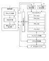
図1は、第1実施形態に係る不揮発性半導体記憶装置の概略構成を示すブロック図である。なお、以下の実施形態では、不揮発性半導体記憶装置としてNAND型フラッシュメモリを例にとる。
図1において、この不揮発性半導体記憶装置には、メモリセルアレイ1、ロウ選択回路2、ウェル電位設定回路3、ソース電位設定回路4、カラム選択回路5、データ入出力バッファ6、制御回路7およびセンスアンプ回路8が設けられている。
(First embodiment)
FIG. 1 is a block diagram showing a schematic configuration of the nonvolatile semiconductor memory device according to the first embodiment. In the following embodiments, a NAND flash memory is taken as an example of the nonvolatile semiconductor memory device.
1, the nonvolatile semiconductor memory device includes a
メモリセルアレイ1には、データを記憶するメモリセルがロウ方向およびカラム方向にマトリックス状に配置されている。なお、1個のメモリセルは、1ビット分のデータを記憶するようにしてもよいし、2ビット以上のデータが記憶できるように多値化されていてもよい。
In the
ここで、メモリセルアレイ1は、n(nは正の整数)個のブロックB1〜Bnに分割されている。なお、各ブロックB1〜Bnは、NANDセルユニットをロウ方向に複数配列することができる。
Here, the
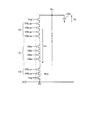
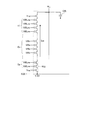
図2は、図1の不揮発性半導体記憶装置のブロックの概略構成を示す回路図である。
図2において、ブロックBi(1≦i≦nの整数)には、l(lは正の整数)本のワード線WL1〜WLl、セレクトゲート線SGD、SGSおよびソース線SCEが設けられている。また、ブロックB1〜Bnには、m(mは正の整数)本のビット線BL1〜BLmが共通に設けられている。
FIG. 2 is a circuit diagram showing a schematic configuration of a block of the nonvolatile semiconductor memory device of FIG.
In FIG. 2, a block Bi (an integer satisfying 1 ≦ i ≦ n) is provided with l (l is a positive integer) word lines WL1 to WLl, select gate lines SGD and SGS, and a source line SCE. Further, m (m is a positive integer) number of bit lines BL1 to BLm are commonly provided in the blocks B1 to Bn.
そして、ブロックBiには、m個のNANDセルユニットNU1〜NUmが設けられ、NANDセルユニットNU1〜NUmはビット線BL1〜BLmにそれぞれ隣接するようにしてロウ方向に配列されている。 The block Bi is provided with m NAND cell units NU1 to NUm, and the NAND cell units NU1 to NUm are arranged in the row direction so as to be adjacent to the bit lines BL1 to BLm, respectively.
ここで、NANDセルユニットNU1〜NUmには、l個のセルトランジスタMT1〜MTlおよびセレクトトランジスタMS1、MS2がそれぞれ設けられている。なお、メモリセルアレイ1の1個のメモリセルには、1個のセルトランジスタMTk(1≦k≦lの整数)を設けることができる。そしてNANDストリングは、直列に接続されたl個のセルトランジスタMT1〜MTlが設けられている。NANDセルユニットNUj(1≦j≦mの整数)は、そのNANDストリングの両端に接続されたセレクトトランジスタMS1、MS2が設けられている。
Here, l cell transistors MT1 to MTl and select transistors MS1 and MS2 are provided in the NAND cell units NU1 to NUm, respectively. Note that one memory cell of the
そして、NANDセルユニットNU1〜NUmにおいて、セルトランジスタMT1〜MTlの制御ゲート電極には、ワード線WL1〜WLlがそれぞれ接続されている。また、NANDセルユニットNUjにおいて、セルトランジスタMT1〜MTlが設けられたNANDストリングの一端は、セレクトトランジスタMS1を介してビット線BLjに接続され、NANDストリングの他端は、セレクトトランジスタMS2を介してソース線SCEに接続されている。 In the NAND cell units NU1 to NUm, word lines WL1 to WLl are connected to the control gate electrodes of the cell transistors MT1 to MTl, respectively. In the NAND cell unit NUj, one end of the NAND string provided with the cell transistors MT1 to MTl is connected to the bit line BLj via the select transistor MS1, and the other end of the NAND string is sourced via the select transistor MS2. Connected to line SCE.
また、図1において、ロウ選択回路2は、メモリセルの読み書き消去時において、メモリセルアレイ1のロウ方向のメモリセルを選択することができる。ウェル電位設定回路3は、メモリセルの読み書き消去時において、メモリセルアレイ1のウェル電位を設定することができる。ソース電位設定回路4は、メモリセルの読み書き消去時において、メモリセルアレイ1のソース電位を設定することができる。カラム選択回路5は、メモリセルの読み書き消去時において、メモリセルアレイ1のカラム方向のメモリセルを選択することができる。センスアンプ回路8は、メモリセルから読み出されたデータをカラムごとに判別することができる。データ入出力バッファ6は、外部から受け取ったコマンドやアドレスを制御回路7に送ったり、センスアンプ回路8と外部との間でデータの授受を行ったりすることができる。
In FIG. 1, the
制御回路7は、コマンドおよびアドレスに基づいて、ロウ選択回路2、ウェル電位設定回路3、ソース電位設定回路4およびカラム選択回路5の動作を制御することができる。ここで、制御回路7には、ブロック分割部7a、消去実行部7bおよび消去ベリファイ実行部7cが設けられている。
The
ブロック分割部7aは、l本のワード線WL1〜WLlをp(pは2以上の整数)個にグルーピングすることで、ブロックBiをp個に分割することができる。すなわち、図2に示すように、ブロックBiをp個に分割することで、p個の分割ブロックD1〜Dpを形成することができる。消去実行部7bは、メモリセルアレイ1のメモリセルに記憶されたデータの消去動作を分割ブロックD1〜Dpごとに実行させることができる。この時、消去実行部7bは、選択ロウのワード線WL1〜WLlよりも高い電圧を非選択ロウのワード線WL1〜WLlに印加させることができる。消去ベリファイ実行部7cは、消去動作が実行されたメモリセルの消去ベリファイ動作を分割ブロックD1〜Dpごとに実行させることができる。
The
そして、ブロックBiの消去動作が実行される場合、分割ブロックDx(xは2≦x≦pの整数)にはワード線WLk−1〜WLk+2に接続されているメモリセルが属するものとすると、分割ブロックDxのワード線WLk−1〜WLk+2に選択ワード線電圧VWeが印加され、それ以外の分割ブロックD1〜Dx−1、Dx+1〜Dpのワード線WL1〜WLk−2、WLk+3〜WLlに非選択ワード線電圧VWLneが印加される。なお、選択ワード線電圧VWeは、例えば、0Vに設定することができる。 When the erase operation of the block Bi is executed, if the memory cells connected to the word lines WLk-1 to WLk + 2 belong to the divided block Dx (x is an integer satisfying 2 ≦ x ≦ p), the division is performed. The selected word line voltage VWe is applied to the word lines WLk-1 to WLk + 2 of the block Dx, and the unselected words are applied to the word lines WL1 to WLk-2 and WLk + 3 to WLl of the other divided blocks D1 to Dx-1, Dx + 1 to Dp. A line voltage VWLne is applied. The selected word line voltage VWe can be set to 0V, for example.
また、メモリセルアレイ1のウェル電位が消去電圧Veに設定される。なお、例えば、消去電圧Veは16〜20V程度に設定することができる。また、ブロックBiのソース線SCEおよびセレクトゲート線SGD、SGSには消去電圧Veを印加することができる。
Further, the well potential of the
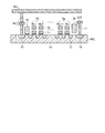
図3は、図1の不揮発性半導体記憶装置の消去動作を示す1セルユニット分の断面図である。
図3において、ウェルWEL上にはフローティングゲート電極15およびセレクトゲート電極19、20が配置され、フローティングゲート電極15上には制御ゲート電極16が配置されている。なお、ウェルWELとフローティングゲート電極15とは、不図示のトンネル絶縁膜を介して絶縁されている。フローティングゲート電極15と制御ゲート電極16とは、不図示の電極間絶縁膜を介して絶縁されている。ここで、1個のフローティングゲート電極15とその上の制御ゲート電極16とで1個のメモリセルを構成することができる。
FIG. 3 is a cross-sectional view of one cell unit showing the erase operation of the nonvolatile semiconductor memory device of FIG.
In FIG. 3, a floating
そして、ウェルWELには、フローティングゲート電極15間、セレクトゲート電極19、20間またはフローティングゲート電極15とセレクトゲート電極19、20との間に配置された不純物拡散層12、13、14が形成されている。なお、例えば、ウェルWELはP型、不純物拡散層12、13、14はN型に形成することができる。
In the well WEL, impurity diffusion layers 12, 13, and 14 are formed between the floating
そして、不純物拡散層13は接続導体18を介してビット線BLjに接続され、不純物拡散層14は接続導体17を介してソース線SCEに接続されている。なお、各メモリセルの制御ゲート電極16はワード線WL1〜WLlに接続され、セレクトゲート電極19、20はセレクトゲート線SGD、SGSにそれぞれ接続されている。
The
そして、分割ブロックDxのワード線WLk−1〜WLk+2に選択ワード線電圧VWeが印加され、それ以外の分割ブロックD1〜Dx−1、Dx+1〜Dpのワード線WL1〜WLk−2、WLk+3〜WLlに非選択ワード線電圧VWLneが印加され、メモリセルアレイ1のウェル電位が消去電圧Veに設定された場合、分割ブロックDxのメモリセルのウェルWELと制御ゲート電極16との間に高電圧がかかる。このため、分割ブロックDxのメモリセルのフローティングゲート電極15に蓄積されていた電子がウェルWEL側に引き抜かれ、分割ブロックDxのメモリセルの消去動作が実行される。
The selected word line voltage VWe is applied to the word lines WLk−1 to WLk + 2 of the divided block Dx, and the word lines WL1 to WLk−2 and WLk + 3 to WLl of the other divided blocks D1 to Dx−1 and Dx + 1 to Dp are applied. When the unselected word line voltage VWLne is applied and the well potential of the
このような消去動作がブロックBiの全ての分割ブロックD1〜Dpについて分割ブロックD1〜Dpごとに繰り返される。 Such an erasing operation is repeated for each of the divided blocks D1 to Dp for all the divided blocks D1 to Dp of the block Bi.
なお、非選択ワード線電圧VWLneは、Ve/2≦VWLne≦Veという条件を満たすことが好ましい。ここで、非選択ワード線電圧VWLneを消去電圧Ve以下に設定することにより、選択ワード線と非選択ワード線との間の電位差に起因する絶縁破壊を防止することができる。非選択ワード線電圧VWLneをVe/2以上に設定することにより、隣接セルと容量カップリングなどによって非選択セルのフローティングゲート電極15の電圧が選択セルのフローティングゲート電極15の電圧に引き込まれるのを抑制することができ、非選択セルの誤消去を防止することができる。
The unselected word line voltage VWLne preferably satisfies the condition Ve / 2 ≦ VWLne ≦ Ve. Here, by setting the unselected word line voltage VWLne to be equal to or lower than the erase voltage Ve, it is possible to prevent dielectric breakdown due to a potential difference between the selected word line and the unselected word line. By setting the non-selected word line voltage VWLne to be equal to or higher than Ve / 2, the voltage of the floating
ブロックBiの全ての分割ブロックD1〜Dpのメモリセルの消去動作が実行されると、消去が完全に行われたかどうかを確認するために、消去ベリファイ動作が実行される。この時、分割ブロックDxのワード線WLk−1〜WLk+2に判定電圧VWLevが印加され、それ以外の分割ブロックD1〜Dx−1、Dx+1〜Dpのワード線WL1〜WLk−2、WLk+3〜WLlに読み出し電圧VWLerが印加される。また、セレクトゲート線SGD、SGSに読み出し電圧Vsgが印加され、ソース線SCEに0Vが印加され、メモリセルアレイ1のウェル電位は0Vに設定される。また、ビット線BLjには、プリチャージ電圧Vpが印加される。また、例えば、判定電圧VWLevは0Vに設定することができる。
When the erase operation of the memory cells of all the divided blocks D1 to Dp of the block Bi is executed, the erase verify operation is executed in order to confirm whether or not the erase has been completely performed. At this time, the determination voltage VWLev is applied to the word lines WLk−1 to WLk + 2 of the divided block Dx, and reading is performed to the word lines WL1 to WLk−2 and WLk + 3 to WLl of the other divided blocks D1 to Dx−1 and Dx + 1 to Dp. A voltage VWLer is applied. Further, the read voltage Vsg is applied to the select gate lines SGD and SGS, 0V is applied to the source line SCE, and the well potential of the
なお、読み出し電圧Vsgは、セレクトトランジスタMS1、MS2をオンさせるのに十分な電圧である。また、読み出し電圧VWLerは、分割ブロックDx以外の分割ブロックD1〜Dx−1、Dx+1〜DpのセルトランジスタMT1〜MTk−2、MTk+3〜MTlをオンさせるのに十分な電圧である。判定電圧VWLevは、分割ブロックDxが消去状態になっているかを判定する電圧である。 The read voltage Vsg is a voltage sufficient to turn on the select transistors MS1 and MS2. The read voltage VWLer is a voltage sufficient to turn on the cell transistors MT1 to MTk-2 and MTk + 3 to MTl of the divided blocks D1 to Dx-1, Dx + 1 to Dp other than the divided block Dx. The determination voltage VWLev is a voltage for determining whether the divided block Dx is in the erased state.
図4は、図1の不揮発性半導体記憶装置の消去ベリファイ動作を示す1セルユニットユニット分の回路図である。
図4において、ビット線BLjには寄生容量CBjが付加されている。そして、分割ブロックDxのセルトランジスタMTk−1〜MTk+2の消去動作を行った結果、セルトランジスタMTk−1〜MTk+2のしきい値電圧が判定電圧VWLev以下になると、消去ベリファイ動作時にNANDセルユニットNUjを介して放電電流Ireが流れ、寄生容量CBjが放電される。この時、ビット線BLjの電位は、最も消去の浅いセルトランジスタMTk−1〜MTk+2のしきい値電圧に依存する。そして、この時のビット線BLjの電位を消去ベリファイ電圧と比較し、ビット線BLjの電位が消去ベリファイ電圧以下の場合は、分割ブロックDxのセルトランジスタMTk−1〜MTk+2の消去が完全に行われたと判断され、ビット線BLjの電位が消去ベリファイ電圧未満の場合は、分割ブロックDxのセルトランジスタMTk−1〜MTk+2の消去が不完全であると判断される。
FIG. 4 is a circuit diagram of one cell unit unit showing the erase verify operation of the nonvolatile semiconductor memory device of FIG.
In FIG. 4, a parasitic capacitance CBj is added to the bit line BLj. As a result of the erase operation of the cell transistors MTk-1 to MTk + 2 in the divided block Dx, if the threshold voltages of the cell transistors MTk-1 to MTk + 2 are equal to or lower than the determination voltage VWLev, the NAND cell unit NUj is set in the erase verify operation. A discharge current Ire flows through the parasitic capacitance CBj. At this time, the potential of the bit line BLj depends on the threshold voltage of the cell transistors MTk-1 to MTk + 2 which are the shallowest erased. Then, the potential of the bit line BLj at this time is compared with the erase verify voltage. If the potential of the bit line BLj is equal to or lower than the erase verify voltage, the cell transistors MTk-1 to MTk + 2 of the divided block Dx are completely erased. When the potential of the bit line BLj is less than the erase verify voltage, it is determined that the erasure of the cell transistors MTk-1 to MTk + 2 of the divided block Dx is incomplete.
このような消去ベリファイ動作がブロックBiの全ての分割ブロックD1〜Dpについて分割ブロックD1〜Dpごとに繰り返される。そして、消去が不完全な分割ブロックD1〜Dpがあると判断された場合、その分割ブロックD1〜Dpについての消去動作および消去ベリファイ動作が繰り返される。 Such an erase verify operation is repeated for each of the divided blocks D1 to Dp for all the divided blocks D1 to Dp of the block Bi. When it is determined that there are divided blocks D1 to Dp that are incompletely erased, the erase operation and erase verify operation for the divided blocks D1 to Dp are repeated.
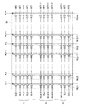
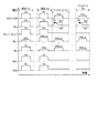
図5は、図1の不揮発性半導体記憶装置のp個の分割ブロックの1回目の消去動作および消去ベリファイ動作を示すタイミングチャートである。
図5において、分割ブロックD1〜Dpの消去動作が順次行われた後、分割ブロックD1〜Dpの消去ベリファイ動作が順次行われる。この時、消去動作の対象とならない分割ブロックD1〜Dpのワード線WL1〜WLlに印加される非選択ワード線電圧VWLneは、消去動作の対象となる分割ブロックD1〜Dpのワード線WL1〜WLlに印加される選択ワード線電圧VWeよりも高くなるように設定される。
FIG. 5 is a timing chart showing the first erase operation and erase verify operation of the p divided blocks of the nonvolatile semiconductor memory device of FIG.
In FIG. 5, after the erase operations of the divided blocks D1 to Dp are sequentially performed, the erase verify operation of the divided blocks D1 to Dp is sequentially performed. At this time, the unselected word line voltage VWLne applied to the word lines WL1 to WLl of the divided blocks D1 to Dp that are not subject to the erase operation is applied to the word lines WL1 to WLl of the divided blocks D1 to Dp that are subject to the erase operation. It is set so as to be higher than the applied selected word line voltage VWe.
また、消去ベリファイ動作の対象とならない分割ブロックD1〜Dpのワード線WL1〜WLlに印加される読み出し電圧VWLerは、消去ベリファイ動作の対象となる分割ブロックD1〜Dpのワード線WL1〜WLlに印加される判定電圧VWLevよりも高くなるように設定される。 Further, the read voltage VWLer applied to the word lines WL1 to WLl of the divided blocks D1 to Dp that are not subject to the erase verify operation is applied to the word lines WL1 to WLl of the divided blocks D1 to Dp that are subject to the erase verify operation. Is set to be higher than the determination voltage VWLev.
そして、ビット線BLjにプリチャージ電圧Vpを印加し、ビット線BLjに充電された電荷がNANDセルユニットNUjを介して放電されるかどうかを判別することにより、各分割ブロックD1〜Dpが消去状態になっているかが判定される。 Then, by applying the precharge voltage Vp to the bit line BLj and determining whether or not the charge charged in the bit line BLj is discharged through the NAND cell unit NUj, each of the divided blocks D1 to Dp is in the erased state. Is determined.
図6は、図1の不揮発性半導体記憶装置の消去動作および消去ベリファイ動作を示すフローチャートである。
図6において、全ての分割ブロックD1〜Dpの検証フラグをNGに設定し(S1)、xを1に設定する(S2)。
FIG. 6 is a flowchart showing the erase operation and erase verify operation of the nonvolatile semiconductor memory device of FIG.
In FIG. 6, the verification flags of all the divided blocks D1 to Dp are set to NG (S1), and x is set to 1 (S2).
そして、xがpでない場合(S3)、分割ブロックDxの検証フラグがOKかNGかを判断し(S4)、分割ブロックDxの検証フラグがNGの場合、分割ブロックDxの消去動作を実行し(S5)、xを1だけインクリメントする(S6)。以上のS3〜S6の動作を全ての分割ブロックD1〜Dpについて繰り返す(S3)。 If x is not p (S3), it is determined whether the verification flag of the divided block Dx is OK or NG (S4). If the verification flag of the divided block Dx is NG, the erase operation of the divided block Dx is executed ( S5), x is incremented by 1 (S6). The operations of S3 to S6 are repeated for all the divided blocks D1 to Dp (S3).
次に、xを1に設定する(S7)。そして、xがpでない場合(S8)、分割ブロックDxの検証フラグがOKかNGかを判断し(S9)、分割ブロックDxの検証フラグがNGの場合、分割ブロックDxの消去ベリファイ動作を実行する(S10)。そして、分割ブロックDxのベリファイチェックがOKの場合(S11)、分割ブロックDxの検証フラグをOKに設定し(S12)、xを1だけインクリメントする(S13)。以上のS8〜S13の動作を全ての分割ブロックD1〜Dpについて繰り返す(S8)。 Next, x is set to 1 (S7). If x is not p (S8), it is determined whether the verification flag of the divided block Dx is OK or NG (S9). If the verification flag of the divided block Dx is NG, the erase verify operation of the divided block Dx is executed. (S10). If the verification check of the divided block Dx is OK (S11), the verification flag of the divided block Dx is set to OK (S12), and x is incremented by 1 (S13). The above operations of S8 to S13 are repeated for all the divided blocks D1 to Dp (S8).
次に、全ての分割ブロックD1〜Dpの検証フラグがOKかどうかを判断し(S14)、全ての分割ブロックD1〜Dpの検証フラグがOKでない場合、消去電圧Veを増加させ(S15)、S2の処理に戻る。全ての分割ブロックD1〜Dpの検証フラグがOKになるまで以上のS2〜S15の動作を繰り返す(S14)。 Next, it is determined whether or not the verification flags of all the divided blocks D1 to Dp are OK (S14). If the verification flags of all the divided blocks D1 to Dp are not OK, the erase voltage Ve is increased (S15), and S2 Return to the process. The above operations S2 to S15 are repeated until the verification flags of all the divided blocks D1 to Dp are OK (S14).
これにより、分割ブロックD1〜Dpごとに消去動作を実行させることが可能となり、消去電圧Veが低い時に消去が完了した分割ブロックD1〜Dpについては高い消去電圧Veが印加されるのを防止することが可能となることから、早めに消去が完了したメモリセルにかかる過剰なストレスを低減することができる。 This makes it possible to execute the erase operation for each of the divided blocks D1 to Dp, and prevents the high erase voltage Ve from being applied to the divided blocks D1 to Dp that have been erased when the erase voltage Ve is low. Therefore, it is possible to reduce excessive stress applied to the memory cell that has been erased early.
また、分割ブロックD1〜Dpごとに消去ベリファイ動作を実行させることにより、消去ベリファイ動作が実行されない分割ブロックD1〜Dpについては、そのセルトランジスタMT1〜MTlをオンさせるために十分な制御ゲート電圧を印加させることができる。このため、ベリファイ読み出し時におけるNANDセルユニットNU1〜NUmのチャネル抵抗を低下させることができ、セルトランジスタMT1〜MTlの閾値が見かけ上増大するのを抑制することが可能となることから、メモリセルの消去が深くなるのを抑制することができる。 Further, by executing the erase verify operation for each of the divided blocks D1 to Dp, a sufficient control gate voltage is applied to turn on the cell transistors MT1 to MTl for the divided blocks D1 to Dp where the erase verify operation is not executed. Can be made. Therefore, the channel resistance of the NAND cell units NU1 to NUm at the time of verify read can be reduced, and it is possible to suppress an apparent increase in the threshold values of the cell transistors MT1 to MTl. Deep erasure can be suppressed.
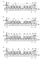
図7は、図1の不揮発性半導体記憶装置のブロック分割方法を示す1セルユニット分の断面図である。
図7(a)に示すように、ブロックBiを1箇所で分離することでブロックBiを2分割するようにしてもよい。また、図7(b)に示すように、ブロックBiを2箇所で分離することでブロックBiを3分割するようにしてもよい。また、図7(c)に示すように、ワード線WL1〜WLlが1つ置きに同一グループに属するようにブロックBiを2分割するようにしてもよい。また、図7(d)に示すように、ワード線WL1〜WLlが2つ置きに同一グループに属するようにブロックBiを2分割するようにしてもよい。
FIG. 7 is a cross-sectional view of one cell unit showing a block division method of the nonvolatile semiconductor memory device of FIG.
As shown in FIG. 7A, the block Bi may be divided into two by separating the block Bi at one place. Further, as shown in FIG. 7B, the block Bi may be divided into three by separating the block Bi at two locations. Further, as shown in FIG. 7C, the block Bi may be divided into two so that every other word line WL1 to WLl belongs to the same group. Further, as shown in FIG. 7D, the block Bi may be divided into two so that every two word lines WL1 to WLl belong to the same group.
ここで、互いに隣接するワード線WL1〜WLlが異なるグループに属するようにブロックBiを分割することにより、消去動作時にワード線WL1〜WLl間で電位差を発生させることが可能となり、ワード線WL1〜WLl間の電子トラップを除去することができる。 Here, by dividing the block Bi so that the word lines WL1 to WLl adjacent to each other belong to different groups, it becomes possible to generate a potential difference between the word lines WL1 to WLl during the erasing operation, and the word lines WL1 to WLl. In between, the electron trap can be removed.
(第2実施形態)
図8は、第2実施形態に係る不揮発性半導体記憶装置の消去動作および消去ベリファイ動作を示すフローチャートである。
図8において、消去ブロックの消去ループ回数または不良ブロック数が規定値未満の場合(S21)、ブロックBiの消去動作および消去ベリファイ動作を実行する(S22、S23)。そして、ベリファイチェックが不合格の場合(S24)、消去電圧Veを増加させ(S25)、ベリファイチェックに合格するまで、ブロックBiについて以上のS22〜S25の動作を繰り返す(S24)。
(Second Embodiment)
FIG. 8 is a flowchart showing the erase operation and erase verify operation of the nonvolatile semiconductor memory device according to the second embodiment.
In FIG. 8, when the number of erase loops or the number of defective blocks in the erase block is less than a specified value (S21), the erase operation and erase verify operation of the block Bi are executed (S22, S23). If the verify check fails (S24), the erase voltage Ve is increased (S25), and the operations of S22 to S25 are repeated for the block Bi until the verify check is passed (S24).
一方、消去ブロックの消去ループ回数または不良ブロック数が規定値以上の場合(S21)、ブロックBiを分割した分割ブロックD1〜Dpごとに消去動作および消去ベリファイ動作を実行する(S26)。なお、このS26の処理は、図6の処理と同様である。ここで、消去ブロックの消去ループ回数とは、消去を行おうとする対象ブロックBiの消去動作の累積回数である。また不良ブロック数とは、不揮発性半導体記憶装置に含まれるブロックのうち、初期または使用により不良と判断したブロックの数である。 On the other hand, if the number of erase loops or the number of defective blocks in the erase block is equal to or greater than the specified value (S21), the erase operation and erase verify operation are executed for each of the divided blocks D1 to Dp obtained by dividing the block Bi (S26). The process of S26 is the same as the process of FIG. Here, the erase block erase loop count is the cumulative number of erase operations of the target block Bi to be erased. The number of defective blocks is the number of blocks determined to be defective in the initial stage or use among the blocks included in the nonvolatile semiconductor memory device.
メモリセルの劣化が進行する前は、ブロック単位で一括消去することが可能となり、消去にかかる時間を短縮することができる。 Before the deterioration of the memory cell progresses, it is possible to erase in a block unit, and the time required for erasing can be shortened.
(第3実施形態)
図9は、第3実施形態に係る不揮発性半導体記憶装置のp個の分割ブロックの1回目の消去動作および消去ベリファイ動作を示すタイミングチャートである。
図5の方法では、消去動作から消去ベリファイ動作に移行する時と、分割ブロックD1〜Dp間で消去ベリファイ動作の移行を行う時に、ビット線BLj−1、BLj、BLj+1の電位を0Vに設定したが、図9の方法では、ビット線BLj−1、BLj、BLj+1の電位がフローティングにされる。
(Third embodiment)
FIG. 9 is a timing chart showing the first erase operation and erase verify operation of p divided blocks of the nonvolatile semiconductor memory device according to the third embodiment.
In the method of FIG. 5, the potentials of the bit lines BLj−1, BLj, and BLj + 1 are set to 0 V when the erase operation is shifted to the erase verify operation and when the erase verify operation is shifted between the divided blocks D1 to Dp. However, in the method of FIG. 9, the potentials of the bit lines BLj−1, BLj, and BLj + 1 are made floating.
ここで、ビット線BLj−1、BLj、BLj+1の電位をフローティングにすることにより、消去動作から消去ベリファイ動作に移行する時と、分割ブロックD1〜Dp間で消去ベリファイ動作の移行を行う時に、ビット線BLj−1、BLj、BLj+1の電位を0Vから上昇させることが可能となる。このため、消去動作から消去ベリファイ動作に移行する時と、分割ブロックD1〜Dp間で消去ベリファイ動作の移行を行う時に、ビット線BLj−1、BLj、BLj+1を放電させたり、再充電させたりする時間を短くすることができ、分割ベリファイ動作を高速化することができる。 Here, when the potentials of the bit lines BLj−1, BLj, and BLj + 1 are floated, when the transition from the erase operation to the erase verify operation is performed and when the erase verify operation is performed between the divided blocks D1 to Dp, The potentials of the lines BLj−1, BLj, and BLj + 1 can be increased from 0V. Therefore, the bit lines BLj−1, BLj, and BLj + 1 are discharged or recharged when the erase operation is shifted to the erase verify operation and when the erase verify operation is shifted between the divided blocks D1 to Dp. The time can be shortened, and the division verify operation can be speeded up.
また、図5の方法では、消去ベリファイ動作時にソース線SCEおよびウェルWELの電圧を0Vに設定したが、図9の方法では、ソース線SCEおよびウェルWELの電圧が判定電圧VWLevよりも増大される。これにより、擬似的に閾値負側に対して読み出すことが可能となり、負側の閾値に対してマージンを確保することができる。 In the method of FIG. 5, the voltages of the source line SCE and the well WEL are set to 0 V during the erase verify operation. However, in the method of FIG. 9, the voltages of the source line SCE and the well WEL are increased from the determination voltage VWLev. . As a result, it is possible to read out the pseudo-threshold value in a pseudo manner, and a margin can be secured for the negative-side threshold value.
(第4実施形態)
図10は、第4実施形態に係る不揮発性半導体記憶装置のp個の分割ブロックの1回目の消去動作および消去ベリファイ動作を示すタイミングチャートである。
図5の方法では、消去ベリファイ動作において、ビット線BLjにプリチャージ電圧Vpを印加し、ビット線BLjに充電された電荷がNANDセルユニットNUjを介して放電されるかどうかを判別することにより、各分割ブロックD1〜Dpが消去状態になっているかを判定した。これに対して、図10の方法では、消去ベリファイ動作において、ソース線SCEに電源電圧VDDを印加し、NANDセルユニットNUjを介してビット線BLjに電荷が充電されるかどうかを判別することにより、各分割ブロックD1〜Dpが消去状態になっているかが判定される。
(Fourth embodiment)
FIG. 10 is a timing chart showing the first erase operation and erase verify operation of p divided blocks of the nonvolatile semiconductor memory device according to the fourth embodiment.
In the method of FIG. 5, in the erase verify operation, by applying a precharge voltage Vp to the bit line BLj and determining whether the charge charged in the bit line BLj is discharged through the NAND cell unit NUj, It was determined whether each of the divided blocks D1 to Dp was in an erased state. On the other hand, in the method of FIG. 10, in the erase verify operation, by applying the power supply voltage VDD to the source line SCE and determining whether or not the bit line BLj is charged through the NAND cell unit NUj. Then, it is determined whether each of the divided blocks D1 to Dp is in the erased state.
これにより、ビット線BLjを充電することで得られるバックバイアス効果を利用して擬似的に閾値負側に対して読み出すことが可能となる。 As a result, it is possible to perform pseudo-reading with respect to the threshold negative side using the back bias effect obtained by charging the bit line BLj.
図11は、図10の不揮発性半導体記憶装置の消去ベリファイ動作を示す1セルユニットユニット分の回路図である。
図11において、分割ブロックDxのセルトランジスタMTk−1〜MTk+2の消去動作を行った結果、セルトランジスタMTk−1〜MTk+2のしきい値電圧が判定電圧VWLev以下になると、消去ベリファイ動作時にセル電流Iceが流れ、寄生容量CBjが充電される。この時、ビット線BLjの電位は、最も消去の浅いセルトランジスタMTk−1〜MTk+2のしきい値電圧に依存する。そして、この時のビット線BLjの電位を消去ベリファイ電圧と比較し、ビット線BLjの電位が消去ベリファイ電圧以上の場合は、セルトランジスタMTk−1〜MTk+2の消去が完全に行われたと判断され、ビット線BLjの電位が消去ベリファイ電圧Vf未満の場合は、セルトランジスタMTk−1〜MTk+2の消去が不完全であると判断される。
FIG. 11 is a circuit diagram of one cell unit unit showing the erase verify operation of the nonvolatile semiconductor memory device of FIG.
In FIG. 11, as a result of the erase operation of the cell transistors MTk-1 to MTk + 2 in the divided block Dx, if the threshold voltages of the cell transistors MTk-1 to MTk + 2 are lower than the determination voltage VWLev, the cell current Ice is generated during the erase verify operation. Flows, and the parasitic capacitance CBj is charged. At this time, the potential of the bit line BLj depends on the threshold voltage of the cell transistors MTk-1 to MTk + 2 which are the shallowest erased. Then, the potential of the bit line BLj at this time is compared with the erase verify voltage. If the potential of the bit line BLj is equal to or higher than the erase verify voltage, it is determined that the cell transistors MTk-1 to MTk + 2 have been completely erased. When the potential of the bit line BLj is lower than the erase verify voltage Vf, it is determined that the erase of the cell transistors MTk-1 to MTk + 2 is incomplete.
本発明のいくつかの実施形態を説明したが、これらの実施形態は、例として提示したものであり、発明の範囲を限定することは意図していない。これら新規な実施形態は、その他の様々な形態で実施されることが可能であり、発明の要旨を逸脱しない範囲で、種々の省略、置き換え、変更を行うことができる。これら実施形態やその変形は、発明の範囲や要旨に含まれるとともに、特許請求の範囲に記載された発明とその均等の範囲に含まれる。 Although several embodiments of the present invention have been described, these embodiments are presented by way of example and are not intended to limit the scope of the invention. These novel embodiments can be implemented in various other forms, and various omissions, replacements, and changes can be made without departing from the scope of the invention. These embodiments and modifications thereof are included in the scope and gist of the invention, and are included in the invention described in the claims and the equivalents thereof.
1 メモリセルアレイ、B1〜Bn ブロック、2 ロウ選択回路、3 ウェル電位設定回路、4 ソース電位設定回路、5 カラム選択回路、6 データ入出力バッファ、7 制御回路、7a ブロック分割部、7b 消去実行部、7c 消去ベリファイ実行部、8 センスアンプ回路、MS1、MS2 セレクトトランジスタ、MT1〜MTl セルトランジスタ、WL1〜WLl ワード線、SGD、SGS セレクトゲート線、SCE ソース線、BL1〜BLm ビット線、NU1〜NUm NANDセルユニット、WEL ウェル、12〜14 不純物拡散層、15 フローティングゲート電極、16 制御ゲート電極、17、18 接続導体、19、20 セレクトゲート電極 1 memory cell array, B1-Bn block, 2 row selection circuit, 3 well potential setting circuit, 4 source potential setting circuit, 5 column selection circuit, 6 data input / output buffer, 7 control circuit, 7a block division unit, 7b erase execution unit , 7c Erase verify execution unit, 8 sense amplifier circuit, MS1, MS2 select transistor, MT1-MTl cell transistor, WL1-WLl word line, SGD, SGS select gate line, SCE source line, BL1-BLm bit line, NU1-NUm NAND cell unit, WEL well, 12-14 impurity diffusion layer, 15 floating gate electrode, 16 control gate electrode, 17, 18 connecting conductor, 19, 20 select gate electrode
Claims (7)
前記l本のワード線をp(pは2以上の整数)個にグルーピングすることで、前記ブロックをp個に分割するブロック分割部と、
選択ロウのワード線よりも非選択ロウのワード線に高い電圧を印加させながら、前記ブロック分割部にて分割された分割ブロックごとに消去動作を実行させる消去実行部と、
前記消去実行部にて消去動作が実行されたブロックにおいて前記分割ブロックごとに消去ベリファイ動作を実行させる消去ベリファイ実行部とを備え、
前記消去ベリファイ実行部は、前記消去実行部にて消去動作が実行された分割ブロックが消去状態になっているかを判定する判定電圧を選択ロウのワード線に印加させるとともに、前記選択ロウのワード線よりも高い電圧を非選択ロウのワード線に印加させ、
前記ブロック単位で消去動作および消去ベリファイ動作を実行し、前記消去動作を規定回数繰り返しても前記ブロックが消去状態にならない時に、前記分割ブロック単位で消去動作および消去ベリファイ動作を実行し、
前記消去ベリファイ実行部は、ビット線に充電された電荷が前記セルユニットを介して放電されるかどうかを判別することにより、前記分割ブロックが消去状態になっているかを判定し、
前記消去動作から前記消去ベリファイ動作に移行する時に前記ビット線の電圧をフローティングにし、
前記消去動作において、ウェルに印加される消去電圧をVeとすると、前記非選択ロウのワード線に印加される電圧VWLneは、Ve/2≦VWLne≦Veという条件を満たすことを特徴とする不揮発性半導体記憶装置。 a memory cell array provided with a block having m (m is an integer of 2 or more) cell units sharing l (l is an integer of 2 or more) word lines;
A block dividing unit for dividing the block into p pieces by grouping the l word lines into p (p is an integer of 2 or more);
An erasing execution unit that executes an erasing operation for each divided block divided by the block dividing unit while applying a higher voltage to a word line of a non-selected row than a word line of a selected row;
An erase verify execution unit that executes an erase verify operation for each of the divided blocks in a block in which an erase operation has been executed by the erase execution unit;
The erase verify execution unit applies a determination voltage to the selected row word line to determine whether the divided block for which the erase operation has been executed by the erase execution unit is in an erased state, and the selected row word line Higher voltage to the word line of the non-selected row,
Performing an erase operation and an erase verify operation in units of blocks, and when the block does not enter an erased state even if the erase operation is repeated a specified number of times, execute an erase operation and an erase verify operation in units of the divided blocks,
The erase verify execution unit determines whether the divided block is in an erased state by determining whether the charge charged in the bit line is discharged through the cell unit,
When shifting from the erase operation to the erase verify operation, the voltage of the bit line is floated,
In the erase operation, if the erase voltage applied to the well is Ve, the voltage VWLne applied to the word line of the unselected row satisfies the condition of Ve / 2 ≦ VWLne ≦ Ve. Semiconductor memory device.
前記l本のワード線をp(pは2以上の整数)個にグルーピングすることで、前記ブロックをp個に分割するブロック分割部と、
選択ロウのワード線よりも非選択ロウのワード線に高い電圧を印加させながら、前記ブロック分割部にて分割された分割ブロックごとに消去動作を実行させる消去実行部と、
前記消去実行部にて消去動作が実行されたブロックにおいて前記分割ブロックごとに消去ベリファイ動作を実行させる消去ベリファイ実行部とを備えることを特徴とする不揮発性半導体記憶装置。 a memory cell array provided with a block having m (m is an integer of 2 or more) cell units sharing l (l is an integer of 2 or more) word lines;
A block dividing unit for dividing the block into p pieces by grouping the l word lines into p (p is an integer of 2 or more);
An erasing execution unit that executes an erasing operation for each divided block divided by the block dividing unit while applying a higher voltage to a word line of a non-selected row than a word line of a selected row;
A non-volatile semiconductor memory device comprising: an erase verify execution unit that executes an erase verify operation for each of the divided blocks in a block for which an erase operation has been executed by the erase execution unit.
Priority Applications (2)
| Application Number | Priority Date | Filing Date | Title |
|---|---|---|---|
| JP2011043795A JP5646369B2 (en) | 2011-03-01 | 2011-03-01 | Nonvolatile semiconductor memory device |
| US13/407,991 US8760935B2 (en) | 2011-03-01 | 2012-02-29 | Nonvolatile semiconductor memory device |
Applications Claiming Priority (1)
| Application Number | Priority Date | Filing Date | Title |
|---|---|---|---|
| JP2011043795A JP5646369B2 (en) | 2011-03-01 | 2011-03-01 | Nonvolatile semiconductor memory device |
Publications (2)
| Publication Number | Publication Date |
|---|---|
| JP2012181890A true JP2012181890A (en) | 2012-09-20 |
| JP5646369B2 JP5646369B2 (en) | 2014-12-24 |
Family
ID=46753215
Family Applications (1)
| Application Number | Title | Priority Date | Filing Date |
|---|---|---|---|
| JP2011043795A Active JP5646369B2 (en) | 2011-03-01 | 2011-03-01 | Nonvolatile semiconductor memory device |
Country Status (2)
| Country | Link |
|---|---|
| US (1) | US8760935B2 (en) |
| JP (1) | JP5646369B2 (en) |
Cited By (2)
| Publication number | Priority date | Publication date | Assignee | Title |
|---|---|---|---|---|
| JP2014110435A (en) * | 2012-12-04 | 2014-06-12 | Samsung Electronics Co Ltd | Nonvolatile memory including memory cell array of three-dimensional structure |
| US9318207B2 (en) | 2014-08-12 | 2016-04-19 | Kabushiki Kaisha Toshiba | Nonvolatile semiconductor memory device and method of operating the same |
Families Citing this family (9)
| Publication number | Priority date | Publication date | Assignee | Title |
|---|---|---|---|---|
| KR102348092B1 (en) * | 2015-09-14 | 2022-01-10 | 에스케이하이닉스 주식회사 | Semiconductor memory device and operating method thereof |
| KR20170037722A (en) | 2015-09-25 | 2017-04-05 | 에스케이하이닉스 주식회사 | Semiconductor apparatus, operating method thereof and data storage device including the same |
| KR102395196B1 (en) | 2017-10-17 | 2022-05-06 | 삼성전자주식회사 | Storage device having parameter calibration function and method of operating the storage device |
| KR20190057701A (en) | 2017-11-20 | 2019-05-29 | 삼성전자주식회사 | Non-volatile memory device and erase method thereof |
| US10964398B2 (en) | 2018-09-28 | 2021-03-30 | Samsung Electronics Co., Ltd. | Memory device and a storage system using the same |
| KR20200036653A (en) | 2018-09-28 | 2020-04-07 | 삼성전자주식회사 | A memory device and a storage system using the same |
| KR20210128231A (en) * | 2020-04-16 | 2021-10-26 | 에스케이하이닉스 주식회사 | Memory device and operating method thereof |
| US11527296B2 (en) | 2020-04-24 | 2022-12-13 | Samsung Electronics Co., Ltd. | Operation method of nonvolatile memory device |
| CN113838514B (en) * | 2020-04-28 | 2024-02-27 | 长江存储科技有限责任公司 | Memory device and erasing and verifying method thereof |
Citations (14)
| Publication number | Priority date | Publication date | Assignee | Title |
|---|---|---|---|---|
| JPH03105795A (en) * | 1989-09-20 | 1991-05-02 | Hitachi Ltd | Semiconductor nonvolatile memory device |
| JPH03181095A (en) * | 1989-12-08 | 1991-08-07 | Hitachi Ltd | Non-volatile semiconductor memory device |
| JPH11273368A (en) * | 1998-03-23 | 1999-10-08 | Toshiba Corp | Non-volatile semiconductor memory |
| JP2000222895A (en) * | 1998-11-26 | 2000-08-11 | Toshiba Corp | Nonvolatile semiconductor memory |
| JP2001085646A (en) * | 1999-09-10 | 2001-03-30 | Toshiba Corp | Nonvolatile semiconductor memory |
| JP2001126489A (en) * | 1999-10-27 | 2001-05-11 | Nec Corp | Flash eeprom and aerasing method for its stored data |
| JP2004185688A (en) * | 2002-11-29 | 2004-07-02 | Toshiba Corp | Nonvolatile semiconductor storage device and its erasure verification method |
| JP2005175070A (en) * | 2003-12-09 | 2005-06-30 | Renesas Technology Corp | Semiconductor device |
| JP2006190440A (en) * | 2004-12-28 | 2006-07-20 | Hynix Semiconductor Inc | Nand flash memory device with changeable block size |
| JP2007305283A (en) * | 2006-05-12 | 2007-11-22 | Hynix Semiconductor Inc | Flash memory device having function for changing selectively size of memory cell block in erasing operation, and its erasing method |
| JP2010507180A (en) * | 2006-10-13 | 2010-03-04 | サンディスク コーポレイション | Partial erase and erase verification in non-volatile memory devices |
| JP2010520571A (en) * | 2007-03-07 | 2010-06-10 | モサイド・テクノロジーズ・インコーポレーテッド | Partial block erase architecture for flash memory |
| JP2011170953A (en) * | 2010-02-17 | 2011-09-01 | Samsung Electronics Co Ltd | Nonvolatile memory, operating method thereof, and memory system incorporating the same |
| JP2012069187A (en) * | 2010-09-22 | 2012-04-05 | Toshiba Corp | Nonvolatile semiconductor memory |
Family Cites Families (11)
| Publication number | Priority date | Publication date | Assignee | Title |
|---|---|---|---|---|
| TW365001B (en) * | 1996-10-17 | 1999-07-21 | Hitachi Ltd | Non-volatile semiconductor memory apparatus and the operation method |
| US5963477A (en) * | 1997-12-09 | 1999-10-05 | Macronix International Co., Ltd. | Flash EPROM erase algorithm with wordline level retry |
| JP3672435B2 (en) * | 1998-04-22 | 2005-07-20 | 富士通株式会社 | Nonvolatile memory device |
| US6496417B1 (en) * | 1999-06-08 | 2002-12-17 | Macronix International Co., Ltd. | Method and integrated circuit for bit line soft programming (BLISP) |
| US7272050B2 (en) * | 2004-08-10 | 2007-09-18 | Samsung Electronics Co., Ltd. | Non-volatile memory device and erase method of the same |
| US7391654B2 (en) | 2005-05-11 | 2008-06-24 | Micron Technology, Inc. | Memory block erasing in a flash memory device |
| US7633813B2 (en) * | 2007-01-23 | 2009-12-15 | Hynix Semiconductor Inc. | Method of performing an erase operation in a non-volatile memory device |
| JP2009048697A (en) | 2007-08-20 | 2009-03-05 | Toshiba Corp | Nand type nonvolatile semiconductor memory |
| JP2009301607A (en) | 2008-06-10 | 2009-12-24 | Toshiba Corp | Nonvolatile semiconductor memory device and method for controlling the same |
| JP5159477B2 (en) | 2008-07-08 | 2013-03-06 | 株式会社東芝 | Nonvolatile semiconductor memory device and erase verification method thereof |
| JP2012027988A (en) | 2010-07-23 | 2012-02-09 | Toshiba Corp | Semiconductor storage device and control method for the same |
-
2011
- 2011-03-01 JP JP2011043795A patent/JP5646369B2/en active Active
-
2012
- 2012-02-29 US US13/407,991 patent/US8760935B2/en active Active
Patent Citations (14)
| Publication number | Priority date | Publication date | Assignee | Title |
|---|---|---|---|---|
| JPH03105795A (en) * | 1989-09-20 | 1991-05-02 | Hitachi Ltd | Semiconductor nonvolatile memory device |
| JPH03181095A (en) * | 1989-12-08 | 1991-08-07 | Hitachi Ltd | Non-volatile semiconductor memory device |
| JPH11273368A (en) * | 1998-03-23 | 1999-10-08 | Toshiba Corp | Non-volatile semiconductor memory |
| JP2000222895A (en) * | 1998-11-26 | 2000-08-11 | Toshiba Corp | Nonvolatile semiconductor memory |
| JP2001085646A (en) * | 1999-09-10 | 2001-03-30 | Toshiba Corp | Nonvolatile semiconductor memory |
| JP2001126489A (en) * | 1999-10-27 | 2001-05-11 | Nec Corp | Flash eeprom and aerasing method for its stored data |
| JP2004185688A (en) * | 2002-11-29 | 2004-07-02 | Toshiba Corp | Nonvolatile semiconductor storage device and its erasure verification method |
| JP2005175070A (en) * | 2003-12-09 | 2005-06-30 | Renesas Technology Corp | Semiconductor device |
| JP2006190440A (en) * | 2004-12-28 | 2006-07-20 | Hynix Semiconductor Inc | Nand flash memory device with changeable block size |
| JP2007305283A (en) * | 2006-05-12 | 2007-11-22 | Hynix Semiconductor Inc | Flash memory device having function for changing selectively size of memory cell block in erasing operation, and its erasing method |
| JP2010507180A (en) * | 2006-10-13 | 2010-03-04 | サンディスク コーポレイション | Partial erase and erase verification in non-volatile memory devices |
| JP2010520571A (en) * | 2007-03-07 | 2010-06-10 | モサイド・テクノロジーズ・インコーポレーテッド | Partial block erase architecture for flash memory |
| JP2011170953A (en) * | 2010-02-17 | 2011-09-01 | Samsung Electronics Co Ltd | Nonvolatile memory, operating method thereof, and memory system incorporating the same |
| JP2012069187A (en) * | 2010-09-22 | 2012-04-05 | Toshiba Corp | Nonvolatile semiconductor memory |
Cited By (4)
| Publication number | Priority date | Publication date | Assignee | Title |
|---|---|---|---|---|
| JP2014110435A (en) * | 2012-12-04 | 2014-06-12 | Samsung Electronics Co Ltd | Nonvolatile memory including memory cell array of three-dimensional structure |
| KR20140071792A (en) * | 2012-12-04 | 2014-06-12 | 삼성전자주식회사 | Nonvolatile memory including memory cell array having 3-dimensional structure |
| KR102021808B1 (en) | 2012-12-04 | 2019-09-17 | 삼성전자주식회사 | Nonvolatile memory including memory cell array having 3-dimensional structure |
| US9318207B2 (en) | 2014-08-12 | 2016-04-19 | Kabushiki Kaisha Toshiba | Nonvolatile semiconductor memory device and method of operating the same |
Also Published As
| Publication number | Publication date |
|---|---|
| US20120224427A1 (en) | 2012-09-06 |
| US8760935B2 (en) | 2014-06-24 |
| JP5646369B2 (en) | 2014-12-24 |
Similar Documents
| Publication | Publication Date | Title |
|---|---|---|
| JP5646369B2 (en) | Nonvolatile semiconductor memory device | |
| TWI649752B (en) | Semiconductor memory device | |
| JP5649560B2 (en) | Nonvolatile semiconductor memory device | |
| JP2014038670A (en) | Nonvolatile semiconductor memory device | |
| JP2012160237A (en) | Nonvolatile semiconductor memory device | |
| JP2012084207A (en) | Nonvolatile semiconductor memory device | |
| JP2014044784A (en) | Semiconductor memory device | |
| CN107093461B (en) | Flash memory device and erasing method thereof | |
| JP2014002810A (en) | Nonvolatile semiconductor memory device | |
| JP2014197442A (en) | Nonvolatile semiconductor memory device and reading method thereof | |
| JP2011181157A (en) | Nonvolatile semiconductor memory device | |
| US9171637B2 (en) | Nonvolatile semiconductor memory device and method of controlling the same | |
| JP2013232262A (en) | Nonvolatile semiconductor memory device | |
| JP2012198966A (en) | Nonvolatile semiconductor memory device and data erasing method for the same | |
| US9208896B2 (en) | Nonvolatile semiconductor memory device | |
| JP2019212351A (en) | Non-volatile semiconductor storage device and rewrite method of non-volatile semiconductor storage device | |
| US20130083602A1 (en) | Nonvolatile semiconductor memory device | |
| JP2012123856A (en) | Nonvolatile semiconductor memory device | |
| JP2020155577A (en) | Semiconductor memory device | |
| US9355714B2 (en) | Nonvolatile semiconductor memory device and method of controlling the same | |
| JP2013246844A (en) | Nonvolatile semiconductor memory device | |
| JP2012203953A (en) | Nonvolatile semiconductor memory device | |
| JP5814961B2 (en) | Nonvolatile semiconductor memory device | |
| JP5619038B2 (en) | Nonvolatile semiconductor memory device | |
| JP5404670B2 (en) | Nonvolatile semiconductor memory device |
Legal Events
| Date | Code | Title | Description |
|---|---|---|---|
| A621 | Written request for application examination |
Free format text: JAPANESE INTERMEDIATE CODE: A621 Effective date: 20130218 |
|
| A977 | Report on retrieval |
Free format text: JAPANESE INTERMEDIATE CODE: A971007 Effective date: 20130610 |
|
| A131 | Notification of reasons for refusal |
Free format text: JAPANESE INTERMEDIATE CODE: A131 Effective date: 20130618 |
|
| A521 | Request for written amendment filed |
Free format text: JAPANESE INTERMEDIATE CODE: A523 Effective date: 20130807 |
|
| A131 | Notification of reasons for refusal |
Free format text: JAPANESE INTERMEDIATE CODE: A131 Effective date: 20140304 |
|
| A521 | Request for written amendment filed |
Free format text: JAPANESE INTERMEDIATE CODE: A523 Effective date: 20140409 |
|
| TRDD | Decision of grant or rejection written | ||
| A01 | Written decision to grant a patent or to grant a registration (utility model) |
Free format text: JAPANESE INTERMEDIATE CODE: A01 Effective date: 20141007 |
|
| A61 | First payment of annual fees (during grant procedure) |
Free format text: JAPANESE INTERMEDIATE CODE: A61 Effective date: 20141105 |
|
| R151 | Written notification of patent or utility model registration |
Ref document number: 5646369 Country of ref document: JP Free format text: JAPANESE INTERMEDIATE CODE: R151 |
|
| S111 | Request for change of ownership or part of ownership |
Free format text: JAPANESE INTERMEDIATE CODE: R313111 |
|
| R350 | Written notification of registration of transfer |
Free format text: JAPANESE INTERMEDIATE CODE: R350 |
|
| S111 | Request for change of ownership or part of ownership |
Free format text: JAPANESE INTERMEDIATE CODE: R313111 |
|
| R350 | Written notification of registration of transfer |
Free format text: JAPANESE INTERMEDIATE CODE: R350 |