JP2012168002A - Minute sample processing method and minute sample - Google Patents
Minute sample processing method and minute sample Download PDFInfo
- Publication number
- JP2012168002A JP2012168002A JP2011028785A JP2011028785A JP2012168002A JP 2012168002 A JP2012168002 A JP 2012168002A JP 2011028785 A JP2011028785 A JP 2011028785A JP 2011028785 A JP2011028785 A JP 2011028785A JP 2012168002 A JP2012168002 A JP 2012168002A
- Authority
- JP
- Japan
- Prior art keywords
- micro sample
- sample
- ion beam
- processing method
- minute sample
- Prior art date
- Legal status (The legal status is an assumption and is not a legal conclusion. Google has not performed a legal analysis and makes no representation as to the accuracy of the status listed.)
- Withdrawn
Links
Images


Abstract
Description
この発明の実施形態は、半導体デバイスの研究や製造における観察・分析・評価のために使用する微小試料の加工方法及び微小試料に関する。 Embodiments described herein relate generally to a micro sample processing method and a micro sample used for observation, analysis, and evaluation in research and manufacture of semiconductor devices.
半導体デバイスの観察用の微小試料を透過型電子顕微鏡(例えば、STEM(Scanning Transmission Electron Microscope)やTEM)で観察する場合、電子の透過方向に観察したい対象物のみを含むように半導体デバイスが形成された基板を薄く加工した微小試料を作成する必要がある。 When a micro sample for observation of a semiconductor device is observed with a transmission electron microscope (for example, STEM (Scanning Transmission Electron Microscope) or TEM), the semiconductor device is formed so as to include only an object to be observed in the electron transmission direction. It is necessary to make a micro sample by thinly processing the substrate.
微小試料の作成には種々の手法があるが、一般的には、FIB(Focused Ion Beam)カラムから電子線を照射して基板から観察対象領域を含む微小試料を切り出し、この切り出した微小試料を基板から取り出して固定し、さらに微小試料を電子の透過方向に観察したい対象物のみを含むようにFIBにより薄く加工することが行われる(例えば、特許文献1参照)。 There are various methods for creating a micro sample. In general, an electron beam is irradiated from a FIB (Focused Ion Beam) column to cut out a micro sample including an observation target region from the substrate, A thin sample is processed by FIB so as to include only an object to be observed in the electron transmission direction after being taken out from the substrate and fixed (see, for example, Patent Document 1).
近年では、半導体デバイスの微細化に伴い微小試料の厚みも薄くする必要が生じており、場合によっては、20nm以下の厚さまで薄く加工する必要がある。しかしながら、微小試料を20nm以下の厚さまで薄く加工した場合、試料の強度が弱くなり、薄く加工した部分によじれが生じる。このよじれにより微小試料の観察対象領域をSTEMもしくはTEMで観察する場合にフォーカス(焦点)が合わず、半導体デバイスを解析できないという問題があった。
本発明が解決しようとする課題は、微小試料に生じる歪みを抑制できる微小試料の加工方法及び微小試料を提供することである。
In recent years, with the miniaturization of semiconductor devices, it has become necessary to reduce the thickness of micro samples, and in some cases, it is necessary to process thinly to a thickness of 20 nm or less. However, when a minute sample is thinly processed to a thickness of 20 nm or less, the strength of the sample is weakened and the thinly processed portion is kinked. Due to this kinking, there is a problem that when the observation target region of the minute sample is observed with the STEM or TEM, the focus is not achieved and the semiconductor device cannot be analyzed.
The problem to be solved by the present invention is to provide a processing method of a micro sample and a micro sample that can suppress distortion generated in the micro sample.
本発明の実施形態に係る微小試料の加工方法は、直方体形状を有する透過型電子顕微鏡の観察用の微小試料の加工方法であって、基板上に形成された半導体デバイスから透過型電子顕微鏡の観察対象領域を含む微小試料を切り出す工程と、微小試料の上面側から収束イオンビームを照射して微小試料の一部を切削し、微小試料の正面側に集束イオンビームの照射方向に対して平行な矩形の第1の平面を形成する第1の切削工程と、第1の平面に対して平行な面内において、第1の切削工程とは異なる角度で微小試料へ収束イオンビームを照射して微小試料の一部を切削し、微小試料の裏面側に第1の平面に対して平行な矩形の第2の平面を形成する第2の切削工程と、を有する。 A processing method of a micro sample according to an embodiment of the present invention is a processing method of a micro sample for observation of a transmission electron microscope having a rectangular parallelepiped shape, and observation of the transmission electron microscope from a semiconductor device formed on a substrate Cutting the micro sample including the target area, irradiating the focused ion beam from the upper surface side of the micro sample, cutting a part of the micro sample, and parallel to the irradiation direction of the focused ion beam on the front side of the micro sample In a plane parallel to the first plane and a first cutting process that forms a rectangular first plane, the focused sample is irradiated with a focused ion beam at a different angle from that of the first cutting process. A second cutting step of cutting a part of the sample to form a rectangular second plane parallel to the first plane on the back side of the micro sample.
以下、図面を参照して、本発明の実施形態を詳細に説明する。 Hereinafter, embodiments of the present invention will be described in detail with reference to the drawings.
(実施形態)
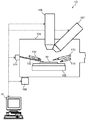
図1は、第1の実施形態に係る観察装置1の構成を示す図である。図1には、観察装置1の具体例として半導体デバイスの構造解析等に用いられるDualBeamFIB装置を示した。観察装置1は、大きく分けて、処理装置10および制御装置20から構成される。処理装置10は、半導体デバイスが形成されたウェハW(半導体基板)から観察対象領域を含む微小試料を切り出す。そして、切り出した微小試料をFIBにより数十nm程度の厚さに切削加工し、透過型電子顕微鏡(例えば、STEMやTEM(以下、単にTEMと称する))により微小試料の断面を撮像する。制御装置20は、処理装置10全体を制御する。
(Embodiment)
FIG. 1 is a diagram illustrating a configuration of an
処理装置10は、搬送ロボット101、ハッチ102、載置台103、搬送ロボット104、試料台105、第1のカラム106、第2のカラム107、真空試料室108、真空ポンプ109などを具備する。搬送ロボット101は、カセット台30上に置かれたカセット40内に収容されているウェハWを真空試料室108内の載置台103へと搬送する。
The
ハッチ102は、搬送ロボット101が載置台103へウェハWを搬送する際にオープン(Open)する。ウェハWが載置台103へ搬送され、搬送ロボット101が安全位置へ退避すると、ハッチ102は、クローズ(Close)する。搬送ロボット104は、載置台103上のウェハWを試料台105上へ搬送する。試料台105は、図示しないステップモータ等により高精度で前後左右へ移動する。試料台105は、ウェハW上の指定箇所が第1のカラム106の真下に来るよう移動する。
The
第1のカラム106および第2のカラム107は、それぞれの中心軸がウェハW表面付近で一点に交わるように真空試料室108へ取り付けられる。第1のカラム106は、内部にイオン源、このイオン源から放出されるイオンビームを集束するレンズおよびイオンビーム走査偏向器等を具備する。第1のカラム106は、試料台105に載置されたウェハW上へ集束イオンビームを照射する。第1のカラム106から照射される集束イオンビームは、ウェハWからの微小試料の切り出しや、切り出した微小試料の加工に用いられる。
The
第2のカラム107は、内部に電子銃、この電子銃から放出される電子線を集束する電子レンズおよび電子ビーム走査偏向器等を具備する。第2のカラム107は、切り出した微小試料へ電子線を照射する。第2のカラム107から照射される電子線は、観察対象である微小試料のTEM画像を得るために用いられる。
The
真空ポンプ109は、真空試料室108内を真空引きし、真空試料室108内を適切な圧力に維持する。尚、第1のカラム106、第2のカラム107にも排気系(図示せず)を個別に具備し、第1のカラム106内、および第2のカラム107内を所望の圧力に維持する。
The
図2は、第1の実施形態に係る観察装置の観察系の詳細構成を示す図である。
図2に示すように、試料台105の周りには、二次電子検出器110、X線検出器111、プローブ112、ガス供給装置113が配置される。また、真空試料室108の外部には、プローブ112を制御するプローブ制御装置114が配置される。
FIG. 2 is a diagram illustrating a detailed configuration of an observation system of the observation apparatus according to the first embodiment.
As shown in FIG. 2, a secondary electron detector 110, an
二次電子検出器110は、ウェハWから放出される二次電子を検出する。二次電子検出器110で検出された二次電子を利用して、微小試料のTEM画像が生成される。X線検出器111は、第2のカラム107から電子線を微小試料へ照射した際に得られるX線(特性X線)を検出する。X線検出器111で検出されたX線を利用して、微小試料のTEM画像が生成される。ガス供給装置113は、ウェハWから切り出した微小試料を固定するための堆積性ガス(例えば、W(タングステン))を供給する。プローブ制御装置114は、プローブ112を制御する。
The secondary electron detector 110 detects secondary electrons emitted from the wafer W. Using the secondary electrons detected by the secondary electron detector 110, a TEM image of the micro sample is generated. The
制御装置20は、例えば、PC(Personal Computer)やCPCI(Compact PCI:登録商標)などであり、ユーザインターフェースとしてのディスプレイ(例えば、LCDやCRT)及び入力手段(例えば、キーボード、マウス)を具備する。ユーザは、制御装置20が具備する入力手段を操作して所望の処理を実現する。
The
次に、ウェハWから切り出した微小試料の加工について説明する。なお、以下に説明する微小試料の加工は、ユーザが、制御装置20が具備する入力手段を操作することにより実施される。
Next, processing of a minute sample cut out from the wafer W will be described. Note that the processing of the micro sample described below is performed by the user operating the input means provided in the
(微小試料の切り出し)
図3は、ウェハWからの微小試料Sの切り出し方法について説明するための図である(図3のハッチングは、ウェハWの表面(半導体デバイス形成面)を表している)。以下、図2,図3を参照してウェハWからの微小試料Sの切り出しについて説明する。なお、ウェハWが試料台105上へ搬送され、真空試料室108内は、所望の圧力まで真空引きされているものとする。
(Cutting out a small sample)
FIG. 3 is a diagram for explaining a method of cutting out the micro sample S from the wafer W (the hatching in FIG. 3 represents the surface of the wafer W (semiconductor device formation surface)). Hereinafter, the cutting of the minute sample S from the wafer W will be described with reference to FIGS. It is assumed that the wafer W is transferred onto the
(第1工程:図3(a)参照)
第1のカラム106から集束イオンビームIをウェハWへ照射してコの字型の溝Cを形成する。
(First step: see FIG. 3A)
A focused ion beam I is irradiated onto the wafer W from the
(第2工程:図3(b)参照)
試料台105を傾斜させることによりウェハWを傾斜させ、集束イオンビームIを照射して三角柱の斜面を形成するように加工する。ただし、この状態では、微小試料SとウェハWとは支持部Bで接続されている。なお、図3(b)では、集束イオンビームIが傾斜した状態で記載しているが、実際には、ウェハWが傾斜している。
(Second step: see FIG. 3B)
The wafer W is tilted by tilting the
(第3工程:図3(c)参照)
試料台105の傾斜を戻した後、プローブ112を微小試料Sの端部に接触させた状態で、ガス供給装置113からWガスを供給しながら、プローブ112の先端と微小試料Sとの接触点に集束イオンビームIを照射するイオンビームアシスト接着により接触点にWの堆積膜Tを形成して、プローブ112の先端を微小試料Sの端部に接合し一体化する。その後、支持部Bを集束イオンビームIで切断する。
(3rd process: Refer FIG.3 (c))
After the inclination of the
(第4工程:図3(d)参照)
最後に、プローブ112を操作して、微小試料SをウェハWから取り出して、微小試料Sの切り出しが完了する。切り出された微小試料Sは、図示しないタングステン(W)等からなるTEMホルダに載置された後、集束イオンビームIにより所望の形状(例えば、立方体)に切削加工される。
(4th process: Refer FIG.3 (d))
Finally, the
なお、図3の説明では、集束イオンビームにより微小試料SをウェハWから切り出す場合について説明したが、ウェハW表面にダイアモンドペン等で傷を付けて劈開するかダイシングソ−を用いて観察対象領域を含む領域を分断した後、この分断した領域をダイヤモンドカッターでスライスし、さらに所望の厚みまで研磨盤上で薄く研磨したものを微小試料Sとしてもよい。なお、このように作製した微小試料Sは、上述のTEMホルダに載置された後、真空試料室108内へ搬送される。
In the description of FIG. 3, the case where the micro sample S is cut out from the wafer W by the focused ion beam has been described. However, the surface of the wafer W is cleaved with a diamond pen etc. After dividing the region to be included, the micro sample S may be obtained by slicing the divided region with a diamond cutter and further polishing it to a desired thickness on a polishing board. The micro sample S produced in this way is placed on the TEM holder described above and then transferred into the
また、図3では、形状が三角柱となるように微小試料Sを切り出しているが、切り出す微小試料Sの形状は、三角柱に限られない。 In FIG. 3, the micro sample S is cut out so that the shape is a triangular prism, but the shape of the micro sample S to be cut out is not limited to a triangular prism.
(微小試料の加工)
次に、切り出した微小試料Sの加工方法について説明する。初めに比較例の加工方法とその問題点ついて説明した後、本実施形態での加工方法について説明する。なお、以下の説明では、切り出した微小試料の形状が集束イオンビームにより直方体に切削されているものとする。
(Micro sample processing)
Next, a method for processing the cut out small sample S will be described. First, after describing the processing method of the comparative example and its problems, the processing method in this embodiment will be described. In the following description, it is assumed that the shape of the cut out micro sample is cut into a rectangular parallelepiped with a focused ion beam.
(比較例の加工方法)
図4は、比較例の微小試料Sの加工方法の説明図である。
以下、図4を参照して比較例の加工方法について説明する。
(Processing method of comparative example)
FIG. 4 is an explanatory diagram of a processing method of the micro sample S of the comparative example.
Hereinafter, the processing method of the comparative example will be described with reference to FIG.
(第1の切削工程:図4(a)参照)
上面F1側から集束イオンビームIを照射して、微小試料Sの正面F2側の一部を切削する。
(First cutting step: see FIG. 4A)
The focused ion beam I is irradiated from the upper surface F1 side, and a part of the front surface F2 side of the micro sample S is cut.
(第2の切削工程:図4(b)参照)
上面F1側から集束イオンビームIを照射して、観察対象領域Xの厚みが所望の厚みとなるように微小試料Sの裏面F3側の一部を切削する。
(Second cutting step: see FIG. 4B)
The focused ion beam I is irradiated from the upper surface F1 side, and a part on the back surface F3 side of the micro sample S is cut so that the thickness of the observation target region X becomes a desired thickness.
(比較例の加工方法の問題点)
次に、比較例の加工方法の問題点について説明する。
図5は、比較例の加工方法による問題点の説明図である。既に述べたように、半導体デバイスの観察用の微小試料をTEMで観察する場合、電子の透過方向に観察したい対象物のみを含むように加工する必要がある。そして、半導体デバイスの微細化に伴い、この厚みも薄くする必要が生じており、場合によっては、20nm以下の厚さまで薄く加工する必要がある。
(Problems of processing method of comparative example)
Next, problems of the processing method of the comparative example will be described.
FIG. 5 is an explanatory diagram of problems caused by the processing method of the comparative example. As already described, when a micro sample for observing a semiconductor device is observed with a TEM, it is necessary to process the sample so as to include only an object to be observed in the electron transmission direction. And with the miniaturization of semiconductor devices, it is necessary to reduce this thickness, and depending on the case, it is necessary to process it to a thickness of 20 nm or less.
しかしながら、観察対象領域Xの材質や大きさにもよるが、観察対象領域Xの厚みD1が20nm以下の厚さになると強度が弱くなるため、観察対象領域Xによじれ(図5の一点鎖線で囲まれた領域A)が生じる。このよじれにより微小試料の観察対象領域をTEMで観察する場合にフォーカス(焦点)が合わず、半導体デバイスを観察できないという問題が生じる。 However, although depending on the material and size of the observation target region X, when the thickness D1 of the observation target region X is 20 nm or less, the strength is weakened. An enclosed area A) results. Due to this kinking, there is a problem that when the observation target region of the minute sample is observed with the TEM, the focus is not achieved and the semiconductor device cannot be observed.
図6は、比較例の加工方法で加工した微小試料の画像である。図6には、観察対象領域の厚みを10nmまで薄く加工した微小試料の画像を示した。なお、図6は、微小試料の上面から撮像した画像である。図6からは、一点鎖線で囲まれた領域Aによじれが生じていることがわかる。 FIG. 6 is an image of a micro sample processed by the processing method of the comparative example. In FIG. 6, the image of the micro sample which processed the thickness of the observation object area | region thinly to 10 nm was shown. FIG. 6 is an image taken from the upper surface of the micro sample. From FIG. 6, it can be seen that the region A surrounded by the alternate long and short dash line is kinked.
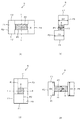
(本実施形態の第1の加工方法)
図7は、本実施形態の微小試料Sの第1の加工方法を説明する図である。
以下、図7を参照して本実施形態の微小試料Sの第1の加工方法を説明する。
(First processing method of this embodiment)
FIG. 7 is a diagram for explaining a first processing method of the micro sample S of the present embodiment.
Hereinafter, the first processing method of the micro sample S of the present embodiment will be described with reference to FIG.
(第1の切削工程:図7(a)参照)
上面F1側から集束イオンビームIを照射して、微小試料Sの正面F2側の一部を切削し、微小試料Sの正面F2側に集束イオンビームIの照射方向に対して平行な四角形の第1の平面P1を形成する。なお、第1の平面P1を形成する際には、微小試料Sの底面F4側の一部を残すことに留意する。
(First cutting step: see FIG. 7A)
The focused ion beam I is irradiated from the upper surface F1 side, a part of the front surface F2 side of the micro sample S is cut, and a rectangular second parallel to the irradiation direction of the focused ion beam I is formed on the front surface F2 side of the micro sample S. 1 plane P1 is formed. It should be noted that when the first plane P1 is formed, a part on the bottom surface F4 side of the micro sample S is left.
正面F2側の切削が完了したら、プローブ112を操作して、微小試料の底面F4が上側となるように微小試料Sを180°回転させる。
When the cutting on the front surface F2 side is completed, the
(第2の切削工程:図7(b)参照)
底面F4側から集束イオンビームIを照射して、微小試料Sの裏面F3側に第1の平面P1に対して平行な四角形の第2の平面P2を形成する。なお、第2の平面P2を形成する際には、微小試料Sの上面F1側の一部を残すことに留意する。また、微小試料Sを切削する際には、第1の平面及び第2の平面との間に観察対象領域が挟まれるように微小試料を加工することに留意する。
(Second cutting step: see FIG. 7B)
The focused ion beam I is irradiated from the bottom surface F4 side, and a rectangular second plane P2 parallel to the first plane P1 is formed on the back surface F3 side of the micro sample S. Note that when the second plane P2 is formed, a part on the upper surface F1 side of the micro sample S is left. Further, when cutting the micro sample S, it is noted that the micro sample is processed so that the observation target region is sandwiched between the first plane and the second plane.
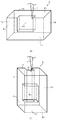
(本実施形態の第1の加工方法による利点)
次に、本実施形態の第1の加工方法による利点について説明する。図8は、本実施形態の第1の加工方法による利点を説明するための図である。図8(a)は、図7を参照して説明した切削後の微小試料Sを上面F1側から見た図である。図8(b)は、図8(a)の線分L−Lにおける微小試料Sの断面図である。図8(c)は、図7を参照して説明した切削後の微小試料Sを右側面F5側から見た図である。図8(d)は、図8(c)の線分L−Lにおける微小試料Sの断面図である。
(Advantages of the first processing method of the present embodiment)
Next, the advantage by the 1st processing method of this embodiment is explained. FIG. 8 is a diagram for explaining advantages of the first processing method of the present embodiment. FIG. 8A is a view of the micro sample S after cutting described with reference to FIG. 7 as viewed from the upper surface F1 side. FIG. 8B is a cross-sectional view of the micro sample S taken along line LL in FIG. FIG.8 (c) is the figure which looked at the microsample S after the cutting demonstrated with reference to FIG. 7 from the right side surface F5 side. FIG. 8D is a cross-sectional view of the micro sample S taken along line LL in FIG.
図8(b)からわかるように、集束イオンビームにより薄く加工された観察対象領域X(ハッチング部)の厚みD1に比べ、上面F1側及び底面F4側における微小試料の厚みD2,D3が厚くなっている。さらに、図8(d)からわかるように、集束イオンビームにより薄く加工された観察対象領域Xの厚みD1に比べ、右側面F5側及び左側面F6側における微小試料の厚みD4,D5が厚くなっている。 As can be seen from FIG. 8B, the thicknesses D2 and D3 of the micro samples on the upper surface F1 side and the bottom surface F4 side are thicker than the thickness D1 of the observation target region X (hatched portion) processed thinly by the focused ion beam. ing. Further, as can be seen from FIG. 8D, the thicknesses D4 and D5 of the micro samples on the right side F5 side and the left side F6 side are thicker than the thickness D1 of the observation target region X processed thinly by the focused ion beam. ing.
すなわち、観察対象領域Xを囲む領域である上面F1側,底面F4側、右側面F5側及び左側面F6側における厚みD2〜D5が観察対象領域Xの厚みD1に比べて厚いため観察対象領域Xの強度が補強される。このため、観察対象領域Xの厚みD1を20nm以下の厚みにまで切削しても観察対象領域Xによじれ等が生じるのを抑制でき、微小試料Sの観察対象領域XをTEMで観察する場合にフォーカス(焦点)が合わず、半導体デバイスを解析できないという問題を低減することができる。なお、微小試料Sの材質や観察対象領域Xの横幅等にもよるが、厚みが20nm以下になると切削した箇所によじれが生じやすいことから、D2〜D5の厚みは、20nmより厚いことが好ましい。 That is, since the thicknesses D2 to D5 on the upper surface F1 side, the bottom surface F4 side, the right side surface F5 side, and the left side surface F6 side that are the regions surrounding the observation target region X are thicker than the thickness D1 of the observation target region X, the observation target region X The strength of is reinforced. For this reason, even when the thickness D1 of the observation target region X is cut to a thickness of 20 nm or less, it is possible to suppress the occurrence of kinking or the like by the observation target region X, and when the observation target region X of the micro sample S is observed with a TEM. It is possible to reduce the problem that the semiconductor device cannot be analyzed because the focus is out of focus. Although depending on the material of the micro sample S, the width of the observation target region X, and the like, the thickness of D2 to D5 is preferably greater than 20 nm because the cut portion is likely to be kinked when the thickness is 20 nm or less. .
(本実施形態の第2の加工方法)
図9は、本実施形態の微小試料Sの第2の加工方法を説明する図である。
以下、図9を参照して本実施形態の微小試料Sの第2の加工方法を説明する。
(Second processing method of this embodiment)
FIG. 9 is a diagram illustrating a second processing method for the micro sample S of the present embodiment.
Hereinafter, the second processing method of the micro sample S of the present embodiment will be described with reference to FIG.
(第1の切削工程:図9(a)参照)
上面F1側から集束イオンビームIを照射して、微小試料Sの正面F2側の一部を切削し、微小試料Sの正面F2側に集束イオンビームIの照射方向に対して平行な四角形の第1の平面P1を形成する。
(First cutting step: see FIG. 9A)
The focused ion beam I is irradiated from the upper surface F1 side, a part of the front surface F2 side of the micro sample S is cut, and a rectangular second parallel to the irradiation direction of the focused ion beam I is formed on the front surface F2 side of the micro sample S. 1 plane P1 is formed.
正面F2側の切削が完了したら、プローブ112を操作して、微小試料の右側面F5又は左側面F6が上側となるように微小試料Sを90°回転させる。なお、図9(a)では、右側面F5側が上側となるように微小試料Sを90°回転させた場合を示した。
When the cutting on the front surface F2 side is completed, the
(第2の切削工程:図9(b)参照)
右側面F5側又は左側面F6から集束イオンビームIを照射して、微小試料Sの裏面F3側に第1の平面P1に対して平行な四角形の第2の平面P2を形成する。図9(b)では、右側面F5側の一部を切削した場合を示した。なお、微小試料Sを切削する際には、第1の平面及び第2の平面との間に観察対象領域が挟まれるように微小試料を加工することに留意する。
(Second cutting step: see FIG. 9B)
The focused ion beam I is irradiated from the right side surface F5 side or the left side surface F6 to form a rectangular second plane P2 parallel to the first plane P1 on the back side F3 side of the micro sample S. FIG. 9B shows a case where a part of the right side surface F5 side is cut. Note that when the minute sample S is cut, the minute sample is processed so that the observation target region is sandwiched between the first plane and the second plane.
この第2の加工方法では、図7を参照して説明した第1の加工方法と異なり、第1の平面P1を形成する際に微小試料Sの底面F4側の一部を残す必要はない。また、第2の平面P2を形成する際にも、微小試料Sの右側面F5側(左側面F6側から切削した場合)又は左側面F6側(右側面F5側から切削した場合)の一部を残す必要はない。 In the second processing method, unlike the first processing method described with reference to FIG. 7, it is not necessary to leave a part on the bottom surface F4 side of the micro sample S when forming the first plane P1. Also, when forming the second plane P2, a part of the right side F5 side (when cut from the left side F6 side) or the left side F6 side (when cut from the right side F5 side) of the micro sample S is also formed. There is no need to leave.
(本実施形態の第2の加工方法による利点)
次に、本実施形態の第2の加工方法による利点について説明する。図10は、本実施形態の第2の加工方法による利点を説明するための図である。図10(a)は、図9を参照して説明した切削後の微小試料Sを上面F1側から見た図である。図10(b)は、図10(a)の線分L−Lにおける微小試料Sの断面図である。図10(c)は、図9を参照して説明した切削後の微小試料Sを右側面F5側から見た図である。図10(d)は、図10(c)の線分L−Lにおける微小試料Sの断面図である。
(Advantages of the second processing method of the present embodiment)
Next, the advantage by the 2nd processing method of this embodiment is explained. FIG. 10 is a diagram for explaining advantages of the second processing method of the present embodiment. FIG. 10A is a view of the micro sample S after cutting described with reference to FIG. 9 as viewed from the upper surface F1 side. FIG. 10B is a cross-sectional view of the micro sample S taken along line LL in FIG. FIG.10 (c) is the figure which looked at the microsample S after the cutting demonstrated with reference to FIG. 9 from the right side surface F5 side. FIG. 10D is a cross-sectional view of the micro sample S taken along line LL in FIG.
図10(b)からわかるように、集束イオンビームにより薄く加工された観察対象領域X(ハッチング部)の厚みD1に比べ、上面F1側及び底面F4側における微小試料の厚みD2,D3が厚くなっている。さらに、図10(d)からわかるように、集束イオンビームにより薄く加工された観察対象領域Xの厚みD1に比べ、右側面F5側及び左側面F6側における微小試料の厚みD4,D5が厚くなっている。 As can be seen from FIG. 10B, the thicknesses D2 and D3 of the micro samples on the top surface F1 side and the bottom surface F4 side are thicker than the thickness D1 of the observation target region X (hatched portion) processed thinly by the focused ion beam. ing. Furthermore, as can be seen from FIG. 10 (d), the thicknesses D4 and D5 of the micro samples on the right side F5 side and the left side F6 side are thicker than the thickness D1 of the observation target region X processed thinly by the focused ion beam. ing.
すなわち、観察対象領域Xを囲む領域である上面F1側,底面F4側、右側面F5側及び左側面F6側における厚みD2〜D5が観察対象領域Xの厚みD1に比べて厚いため観察対象領域Xの強度が補強される。このため、観察対象領域Xの厚みD1を20nm以下の厚みにまで切削しても観察対象領域Xによじれ等が生じるのを抑制でき、微小試料Sの観察対象領域XをTEMで観察する場合にフォーカス(焦点)が合わず、半導体デバイスを解析できないという問題を低減することができる。なお、微小試料Sの材質や観察対象領域Xの横幅等にもよるが、厚みが20nm以下になると切削した箇所によじれが生じやすいことから、D2〜D5の厚みは、20nmより厚いことが好ましい。 That is, since the thicknesses D2 to D5 on the upper surface F1 side, the bottom surface F4 side, the right side surface F5 side, and the left side surface F6 side that are the regions surrounding the observation target region X are thicker than the thickness D1 of the observation target region X, the observation target region X The strength of is reinforced. For this reason, even when the thickness D1 of the observation target region X is cut to a thickness of 20 nm or less, it is possible to suppress the occurrence of kinking or the like by the observation target region X, and when the observation target region X of the micro sample S is observed with a TEM. It is possible to reduce the problem that the semiconductor device cannot be analyzed because the focus is out of focus. Although depending on the material of the micro sample S, the width of the observation target region X, and the like, the thickness of D2 to D5 is preferably greater than 20 nm because the cut portion is likely to be kinked when the thickness is 20 nm or less. .
以上のように、本実施形態の加工方法は、ウェハWから切り出した透過型電子顕微鏡による観察対象領域を含む微小試料Sに対して、上面F1側から収束イオンビームIを照射して微小試料Sの一部を切削し、微小試料Sの正面F2側に集束イオンビームIの照射方向に対して平行な第1の平面P1を形成する第1の工程と、第1の平面P1に対して平行な面内において、第1の工程とは異なる角度で微小試料Sへ収束イオンビームIを照射して微小試料Sの一部を切削し、微小試料Sの裏面F3側に第1の平面P1に対して平行な第2の平面P2を形成する第2の工程とから構成される。 As described above, the processing method according to the present embodiment irradiates the micro sample S including the observation target region by the transmission electron microscope cut out from the wafer W with the focused ion beam I from the upper surface F1 side. And a first step of forming a first plane P1 parallel to the irradiation direction of the focused ion beam I on the front surface F2 side of the micro sample S, and parallel to the first plane P1. In this plane, the focused sample is irradiated with the focused ion beam I at an angle different from that of the first step to cut a part of the minute sample S, and the first surface P1 is formed on the back surface F3 side of the minute sample S. And a second step of forming a second plane P2 parallel to the second plane P2.
このように切削することで観察対象領域Xを囲む領域の厚みを観察対象領域Xの厚みD1に比べて厚くすることができ、観察対象領域Xの強度が補強される。このため、観察対象領域Xの厚みD1を薄く(例えば、厚み20nm以下)した場合でも観察対象領域Xによじれ等が生じるのを抑制でき、微小試料Sの観察対象領域XをTEMで観察する場合にフォーカス(焦点)が合わず、半導体デバイスを解析できないという問題を低減することができる。 By cutting in this way, the thickness of the region surrounding the observation target region X can be made larger than the thickness D1 of the observation target region X, and the strength of the observation target region X is reinforced. For this reason, even when the thickness D1 of the observation target region X is thin (for example, a thickness of 20 nm or less), it is possible to suppress the occurrence of kinking and the like by the observation target region X, and Therefore, it is possible to reduce the problem that the semiconductor device cannot be analyzed.
(その他の実施形態)
なお、本発明は上記実施形態そのままに限定されるものではなく、実施段階ではその要旨を逸脱しない範囲で構成要素を変形して具体化できる。例えば、図7,図9では、立体形状が直方体の微小試料Sを切削しているが、上記本実施形態の第1,第2の加工方法は、他の立体形状(例えば、円柱や四面体)の微小試料の加工においても適用可能である。
(Other embodiments)
Note that the present invention is not limited to the above-described embodiment as it is, and can be embodied by modifying the constituent elements without departing from the scope of the invention in the implementation stage. For example, in FIG. 7 and FIG. 9, the micro sample S having a three-dimensional shape is cut, but the first and second processing methods of the present embodiment are different in other three-dimensional shape (for example, a cylinder or a tetrahedron). It can also be applied to the processing of small samples.
また、第2の切削工程における集束イオンビームを照射する角度は、第1の平面P1に対して平行な面内において、第1の切削工程と180°又は90°異なる角度に限られない。微小試料Sの正面F1又は裏面F2の少なくとも一方に観察対象領域Xよりも厚みが厚い部分が観察対象領域Xを取り囲むように形成されていれば180°又は90°以外の角度(例えば、45°)でもよい。 Further, the angle at which the focused ion beam is irradiated in the second cutting process is not limited to an angle different from the first cutting process by 180 ° or 90 ° in a plane parallel to the first plane P1. If a portion thicker than the observation target region X is formed on at least one of the front surface F1 or the back surface F2 of the micro sample S so as to surround the observation target region X, an angle other than 180 ° or 90 ° (for example, 45 °) )
1…観察装置、10…処理装置、20…制御装置、21…本体部、22…モニタ、23…入力部、30…カセット台、40…カセット、101…搬送ロボット、102…ハッチ、103…載置台、104…搬送ロボット、105…試料台、106…第1のカラム、107…第2のカラム、108…真空試料室、109…真空ポンプ、110…二次電子検出器、111…X線検出器、112…プローブ、113…ガス供給装置、114…プローブ制御装置、A…領域、B…支持部、C…溝、D…厚み、F1…上面、F2…正面、F3…裏面、F4…底面、F5…右側面、F6…左側面、I…集束イオンビーム、P1…第1の平面、P2…第2の平面、S…微小試料、T…堆積膜、W…ウェハ、X…観察対象領域。
DESCRIPTION OF
Claims (5)
基板上に形成された半導体デバイスから前記透過型電子顕微鏡の観察対象領域を含む前記微小試料を切り出す工程と、
前記微小試料の上面側から収束イオンビームを照射して前記微小試料の一部を切削し、前記微小試料の正面側に前記集束イオンビームの照射方向に対して平行な矩形の第1の平面を形成する第1の切削工程と、
前記第1の平面に対して平行な面内において、前記第1の切削工程とは異なる角度で前記微小試料へ収束イオンビームを照射して前記微小試料の一部を切削し、前記微小試料の裏面側に前記第1の平面に対して平行な矩形の第2の平面を形成する第2の切削工程と、
を有する微小試料の加工方法。 A processing method of a micro sample for observation of a transmission electron microscope having a rectangular parallelepiped shape,
Cutting out the minute sample including the observation target region of the transmission electron microscope from a semiconductor device formed on a substrate;
A focused ion beam is irradiated from the upper surface side of the micro sample to cut a part of the micro sample, and a rectangular first plane parallel to the irradiation direction of the focused ion beam is formed on the front side of the micro sample. A first cutting step to be formed;
In a plane parallel to the first plane, the micro sample is irradiated with a focused ion beam at an angle different from that of the first cutting step to cut a part of the micro sample, and A second cutting step of forming a rectangular second plane parallel to the first plane on the back side;
A processing method of a micro sample having
前記微小試料の正面側に、前記微小試料の上面側から収束イオンビームを照射して形成された前記集束イオンビームの照射方向に対して平行な矩形の第1の平面と、
前記微小試料の裏面側に、前記第1の平面に対して平行な面内において、前記第1の切削工程とは異なる角度で前記微小試料へ収束イオンビームを照射して形成された前記第1の平面に対して平行な矩形の第2の平面と、
を具備する微小試料。 A micro sample for observation of a transmission electron microscope having a rectangular parallelepiped shape,
A rectangular first plane parallel to the irradiation direction of the focused ion beam formed by irradiating the front side of the micro sample with a focused ion beam from the upper surface side of the micro sample;
The first sample is formed by irradiating the micro sample with a focused ion beam at a different angle from the first cutting step in a plane parallel to the first plane on the back surface side of the micro sample. A rectangular second plane parallel to the plane of
A micro sample comprising:
Priority Applications (1)
| Application Number | Priority Date | Filing Date | Title |
|---|---|---|---|
| JP2011028785A JP2012168002A (en) | 2011-02-14 | 2011-02-14 | Minute sample processing method and minute sample |
Applications Claiming Priority (1)
| Application Number | Priority Date | Filing Date | Title |
|---|---|---|---|
| JP2011028785A JP2012168002A (en) | 2011-02-14 | 2011-02-14 | Minute sample processing method and minute sample |
Publications (1)
| Publication Number | Publication Date |
|---|---|
| JP2012168002A true JP2012168002A (en) | 2012-09-06 |
Family
ID=46972316
Family Applications (1)
| Application Number | Title | Priority Date | Filing Date |
|---|---|---|---|
| JP2011028785A Withdrawn JP2012168002A (en) | 2011-02-14 | 2011-02-14 | Minute sample processing method and minute sample |
Country Status (1)
| Country | Link |
|---|---|
| JP (1) | JP2012168002A (en) |
Cited By (4)
| Publication number | Priority date | Publication date | Assignee | Title |
|---|---|---|---|---|
| US20120189813A1 (en) * | 2010-07-30 | 2012-07-26 | Carl Zeiss Nts Gmbh | TEM-Lamella, Process for its Manufacture, and Apparatus for Executing the Process |
| CN106018022A (en) * | 2016-05-17 | 2016-10-12 | 上海华力微电子有限公司 | Preparation method of planar TEM (transmission electron microscope) sample |
| CN114008437A (en) * | 2019-06-18 | 2022-02-01 | Xyall私人有限公司 | Dissection device |
| CN114279784A (en) * | 2021-12-22 | 2022-04-05 | 上海季丰电子股份有限公司 | Preparation method of transmission electron microscope sample |
-
2011
- 2011-02-14 JP JP2011028785A patent/JP2012168002A/en not_active Withdrawn
Cited By (5)
| Publication number | Priority date | Publication date | Assignee | Title |
|---|---|---|---|---|
| US20120189813A1 (en) * | 2010-07-30 | 2012-07-26 | Carl Zeiss Nts Gmbh | TEM-Lamella, Process for its Manufacture, and Apparatus for Executing the Process |
| US9103753B2 (en) * | 2010-07-30 | 2015-08-11 | Carl Zeiss Microscopy Gmbh | TEM-lamella, process for its manufacture, and apparatus for executing the process |
| CN106018022A (en) * | 2016-05-17 | 2016-10-12 | 上海华力微电子有限公司 | Preparation method of planar TEM (transmission electron microscope) sample |
| CN114008437A (en) * | 2019-06-18 | 2022-02-01 | Xyall私人有限公司 | Dissection device |
| CN114279784A (en) * | 2021-12-22 | 2022-04-05 | 上海季丰电子股份有限公司 | Preparation method of transmission electron microscope sample |
Similar Documents
| Publication | Publication Date | Title |
|---|---|---|
| CN107084869B (en) | High throughput TEM fabrication process and hardware for backside thinning of cross-sectional view thin layers | |
| Echlin et al. | A new TriBeam system for three-dimensional multimodal materials analysis | |
| KR101249134B1 (en) | Charged particle beam apparatus | |
| KR102056507B1 (en) | Charged particle beam device and specimen observation method | |
| JP6780957B2 (en) | Method for preparing a sample for microstructure diagnosis and sample for microstructure diagnosis | |
| CN109256312B (en) | Method for in situ preparation of microscope samples | |
| JP5222507B2 (en) | Ion beam processing apparatus and sample processing method | |
| JP7340363B2 (en) | Apparatus and method for preparing microscopic specimens | |
| US8191168B2 (en) | Method of preparing a transmission electron microscope sample and a sample piece for a transmission electron microscope | |
| JP6974820B2 (en) | Charged particle beam device, sample processing method | |
| JP2012168002A (en) | Minute sample processing method and minute sample | |
| JP6207081B2 (en) | Focused ion beam device | |
| US9260782B2 (en) | Sample preparation method | |
| JP2009216534A (en) | Thin-film sample preparation method | |
| JP2007018928A (en) | Charged particle beam device | |
| JP2013101138A (en) | Cross-sectional observation method of cosmetic | |
| CN105424428B (en) | Auto slice is with checking undercut | |
| US20220157560A1 (en) | Method and device for preparing a microscopic sample from a volume sample | |
| KR20180109687A (en) | Charged particle beam apparatus | |
| JP7152757B2 (en) | Sample processing observation method | |
| JP7141682B2 (en) | SAMPLE MANUFACTURING DEVICE AND METHOD FOR MANUFACTURING SAMPLE | |
| JP2012132813A (en) | Transmission electron microscope specimen and method for preparing the same | |
| JP7214262B2 (en) | Charged particle beam device, sample processing method | |
| JP2016143532A (en) | Charged particle beam device and defect inspection system | |
| US20240071720A1 (en) | Method and system for preparing a specimen |
Legal Events
| Date | Code | Title | Description |
|---|---|---|---|
| A300 | Withdrawal of application because of no request for examination |
Free format text: JAPANESE INTERMEDIATE CODE: A300 Effective date: 20140513 |