JP2012164633A - Led driving device, and led illuminating device - Google Patents
Led driving device, and led illuminating device Download PDFInfo
- Publication number
- JP2012164633A JP2012164633A JP2011239939A JP2011239939A JP2012164633A JP 2012164633 A JP2012164633 A JP 2012164633A JP 2011239939 A JP2011239939 A JP 2011239939A JP 2011239939 A JP2011239939 A JP 2011239939A JP 2012164633 A JP2012164633 A JP 2012164633A
- Authority
- JP
- Japan
- Prior art keywords
- led
- current
- driving device
- control circuit
- circuit
- Prior art date
- Legal status (The legal status is an assumption and is not a legal conclusion. Google has not performed a legal analysis and makes no representation as to the accuracy of the status listed.)
- Granted
Links
Images


Classifications
-
- H—ELECTRICITY
- H05—ELECTRIC TECHNIQUES NOT OTHERWISE PROVIDED FOR
- H05B—ELECTRIC HEATING; ELECTRIC LIGHT SOURCES NOT OTHERWISE PROVIDED FOR; CIRCUIT ARRANGEMENTS FOR ELECTRIC LIGHT SOURCES, IN GENERAL
- H05B45/00—Circuit arrangements for operating light-emitting diodes [LED]
- H05B45/30—Driver circuits
- H05B45/37—Converter circuits
- H05B45/3725—Switched mode power supply [SMPS]
- H05B45/385—Switched mode power supply [SMPS] using flyback topology
-
- H—ELECTRICITY
- H05—ELECTRIC TECHNIQUES NOT OTHERWISE PROVIDED FOR
- H05B—ELECTRIC HEATING; ELECTRIC LIGHT SOURCES NOT OTHERWISE PROVIDED FOR; CIRCUIT ARRANGEMENTS FOR ELECTRIC LIGHT SOURCES, IN GENERAL
- H05B45/00—Circuit arrangements for operating light-emitting diodes [LED]
- H05B45/30—Driver circuits
- H05B45/37—Converter circuits
-
- Y—GENERAL TAGGING OF NEW TECHNOLOGICAL DEVELOPMENTS; GENERAL TAGGING OF CROSS-SECTIONAL TECHNOLOGIES SPANNING OVER SEVERAL SECTIONS OF THE IPC; TECHNICAL SUBJECTS COVERED BY FORMER USPC CROSS-REFERENCE ART COLLECTIONS [XRACs] AND DIGESTS
- Y02—TECHNOLOGIES OR APPLICATIONS FOR MITIGATION OR ADAPTATION AGAINST CLIMATE CHANGE
- Y02B—CLIMATE CHANGE MITIGATION TECHNOLOGIES RELATED TO BUILDINGS, e.g. HOUSING, HOUSE APPLIANCES OR RELATED END-USER APPLICATIONS
- Y02B20/00—Energy efficient lighting technologies, e.g. halogen lamps or gas discharge lamps
- Y02B20/30—Semiconductor lamps, e.g. solid state lamps [SSL] light emitting diodes [LED] or organic LED [OLED]
-
- Y—GENERAL TAGGING OF NEW TECHNOLOGICAL DEVELOPMENTS; GENERAL TAGGING OF CROSS-SECTIONAL TECHNOLOGIES SPANNING OVER SEVERAL SECTIONS OF THE IPC; TECHNICAL SUBJECTS COVERED BY FORMER USPC CROSS-REFERENCE ART COLLECTIONS [XRACs] AND DIGESTS
- Y02—TECHNOLOGIES OR APPLICATIONS FOR MITIGATION OR ADAPTATION AGAINST CLIMATE CHANGE
- Y02B—CLIMATE CHANGE MITIGATION TECHNOLOGIES RELATED TO BUILDINGS, e.g. HOUSING, HOUSE APPLIANCES OR RELATED END-USER APPLICATIONS
- Y02B20/00—Energy efficient lighting technologies, e.g. halogen lamps or gas discharge lamps
- Y02B20/72—Energy efficient lighting technologies, e.g. halogen lamps or gas discharge lamps in street lighting
Landscapes
- Circuit Arrangement For Electric Light Sources In General (AREA)
- Dc-Dc Converters (AREA)
- Led Devices (AREA)
Abstract
Description
本発明は、LED駆動装置及びこれを用いたLED照明装置に関する。 The present invention relates to an LED driving device and an LED lighting device using the same.
LED(Light Emission Diode)素子は、液晶表示装置のバックライト、或いは街路灯等の照明器具の光源として利用され始めている。特に、白熱電球や蛍光灯を代替する照明器具として、白色LED素子を用いた蛍光灯型又は電球型のLED照明装置の開発が進められている。このようなLED照明装置を構成するLED駆動装置は、LED素子に所望の電力を精度良く供給することが求められる。 An LED (Light Emission Diode) element has begun to be used as a light source for a backlight of a liquid crystal display device or a lighting fixture such as a street lamp. In particular, as a lighting fixture that replaces an incandescent bulb and a fluorescent lamp, a fluorescent lamp type or a bulb type LED lighting apparatus using a white LED element has been developed. The LED driving device constituting such an LED lighting device is required to supply desired power to the LED element with high accuracy.
図4は、従来のLED駆動装置101及びLED照明装置110の回路構成を示す回路図である。従来のLED駆動装置101は、整流回路DB100と、トランスTR100と、MOSFET(スイッチング素子)Q101と、ダイオードD101及びコンデンサC101から構成される整流平滑回路と、制御回路CNT100と、コンデンサC103と、を備える。LED駆動装置101とLED負荷102(LED1、・・・LEDn)とは、従来のLED照明装置110を構成する。
FIG. 4 is a circuit diagram illustrating a circuit configuration of the conventional
整流回路DB100は、周知のダイオードブリッジ回路であり、交流入力電源AC100に接続される。トランスTR100は、一次巻線W101と二次巻線W102と三次巻線W103とを有する。一次巻線W101の一端は、整流回路DB100に接続され、一次巻線W101の他端は、MOSFETQ101のドレイン端子に接続される。二次巻線W102の両端は、整流平滑回路に接続される。三次巻線W103の両端は、ダイオードD102及びコンデンサC102から構成される補助電源に接続される。 The rectifier circuit DB100 is a known diode bridge circuit and is connected to the AC input power supply AC100. Transformer TR100 has primary winding W101, secondary winding W102, and tertiary winding W103. One end of the primary winding W101 is connected to the rectifier circuit DB100, and the other end of the primary winding W101 is connected to the drain terminal of the MOSFET Q101. Both ends of the secondary winding W102 are connected to a rectifying / smoothing circuit. Both ends of the tertiary winding W103 are connected to an auxiliary power source composed of a diode D102 and a capacitor C102.
MOSFETQ101のソース端子は接地され、ゲート端子は制御回路CNT100に接続される。整流平滑回路の両端は、直列接続されたn個のLED素子(LED1、・・・LEDn)から構成されるLED負荷102と検出抵抗Rs100との直列回路に接続される。なお、nは1以上の自然数である。
The source terminal of the MOSFET Q101 is grounded, and the gate terminal is connected to the control circuit CNT100. Both ends of the rectifying / smoothing circuit are connected to a series circuit of an
制御回路CNT100の各端子は、MOSFETQ101のゲート端子と、補助電源とLED負荷102及び検出抵抗Rs100の接続点と、コンデンサC103と、に接続され、抵抗R101を介して整流回路DB100及び一次巻線W101の接続点に接続される。制御回路CNT100は、誤差増幅器AMP101と、比較器CMP100と、を備える。
Each terminal of the control circuit CNT100 is connected to the gate terminal of the MOSFET Q101, the connection point between the auxiliary power supply, the
誤差増幅器AMP101の反転入力端子は、LED負荷102及び検出抵抗Rs100の接続点に接続され、非反転入力端子は定電流源REGとツェナーダイオードZD101とから構成される基準電圧に接続される。誤差増幅器AMP101の出力端子は、抵抗R103及びコンデンサC103から構成される積分回路を介して比較器CMP100の第1の非反転入力端子に接続される。誤差増幅器AMP101は、LED負荷102に流れる電流と基準値とに基づく誤差信号を比較器CMP100に出力する。
The inverting input terminal of the error amplifier AMP101 is connected to the connection point between the
比較器CMP100の反転入力端子は、三角波生成回路に接続され、第2の非反転入力端子は、定電流源REGと抵抗R104及びR105とから構成されるDUTY制限回路に接続される。比較器CMP100の出力端子はドライバ回路を介してMOSFETQ101のゲート端子に接続される。比較器CMP100は、誤差増幅器AMP101から出力される誤差信号と三角波生成回路から出力される三角波とに基づくPWM信号をドライバ回路に出力する。 The inverting input terminal of the comparator CMP100 is connected to a triangular wave generating circuit, and the second non-inverting input terminal is connected to a DUTY limiting circuit including a constant current source REG and resistors R104 and R105. The output terminal of the comparator CMP100 is connected to the gate terminal of the MOSFET Q101 through a driver circuit. The comparator CMP100 outputs a PWM signal based on the error signal output from the error amplifier AMP101 and the triangular wave output from the triangular wave generation circuit to the driver circuit.
上記のように構成される従来のLED駆動装置101は、制御回路CNT100がLED負荷102に流れる電流が基準値(基準電圧)になるようにMOSFETQ101をオンオフ制御することで、LED負荷102に印加する電圧を調整する。
The conventional
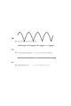
図5は、従来のLED駆動装置101及びLED照明装置110における各部の電圧及び電流の関係を示す波形図である。従来のLED駆動装置101は、交流入力電力を直流電力に変換してLED負荷102に供給するため、入力電圧Vin100のリプル(脈流)が出力電圧Vout100(コンデンサC101の両端電圧)に影響しやすく、出力電圧Vout100は微小な電圧変動を含む。また、LED素子の順方向電流(If)は、順
方向電圧(Vf)に対して指数関数的に増大するという特性を有する。従って、LED負荷102に流れるLED電流ILED100(順方向電流)は、上記の微小な電圧変動に
より大きな電流変化を引き起こす。その結果、従来のLED駆動装置は、LED電流IL
ED100の変化が大きくなりLED負荷102の発光が不安定になりやすいという問題
がある。従来のLED駆動装置において、コンデンサC101の容量を大きくすることで上記の電流変化を低減することができるが、大型の電解コンデンサが必要となり回路の小型化が困難になる。
FIG. 5 is a waveform diagram showing the relationship between the voltage and current of each part in the conventional
There is a problem that the change of the ED 100 becomes large and the light emission of the
図6は、従来の他のLED駆動装置及びこれを用いたLED照明装置の回路構成を示す回路図である。図6に示す従来のLED駆動装置は、PFC(力率改善)回路とPFC回路に接続される電力変換回路との2つのコンバータから構成されるLED点灯装置である。 FIG. 6 is a circuit diagram showing a circuit configuration of another conventional LED driving device and an LED lighting device using the same. The conventional LED driving device shown in FIG. 6 is an LED lighting device composed of two converters, a PFC (power factor correction) circuit and a power conversion circuit connected to the PFC circuit.
PFC回路は、力率を改善するもので、トランスTR100と、MOSFET(スイッチング素子)Q101と、ダイオードD101及びコンデンサC101から構成される整流平滑回路と、制御回路CNT100と、抵抗R107,108と、を備える。電力変換回路は、トランスTR200と、MOSFET(スイッチング素子)Q201と、ダイオードD201及びコンデンサC201から構成される整流平滑回路と、制御回路CNT200と、を備える。 The PFC circuit improves the power factor, and includes a transformer TR100, a MOSFET (switching element) Q101, a rectifying / smoothing circuit composed of a diode D101 and a capacitor C101, a control circuit CNT100, and resistors R107 and 108. Prepare. The power conversion circuit includes a transformer TR200, a MOSFET (switching element) Q201, a rectifying / smoothing circuit including a diode D201 and a capacitor C201, and a control circuit CNT200.
図6に示すLED駆動装置は、電力変換回路の他にPFC回路が設けられているので、高効率な電力変換が行えるとともに、図7に示すように、PFC回路からの出力電圧Vout1と電力変換回路の出力電圧Vout2との2つのステージで、交流入力電圧波形のリプルを低減できる。このため、LED負荷に流れる電流リプルを容易に低減することができる。 The LED driving device shown in FIG. 6 is provided with a PFC circuit in addition to the power conversion circuit, so that highly efficient power conversion can be performed and, as shown in FIG. 7, the output voltage Vout1 from the PFC circuit and the power conversion The ripple of the AC input voltage waveform can be reduced in two stages with the output voltage Vout2 of the circuit. For this reason, the current ripple which flows into LED load can be reduced easily.
しかしながら、2つのコンバータを用いているため、高効率化が困難であり、しかも高価で回路が大型化するという課題を有していた。 However, since two converters are used, it is difficult to achieve high efficiency, and there is a problem that the circuit becomes large due to its high cost.
先行特許1には、交流入力電源に接続された交流/直流変換器と、交流/直流変換器の直流出力電力を変換してLED素子に所望の直流電力を供給する直流/直流変換器と、LED素子に流れる電流を調整するための電流フィードバック部と、を備える別の従来のLED駆動装置が記載される。 Prior Patent 1 includes an AC / DC converter connected to an AC input power source, a DC / DC converter that converts a DC output power of the AC / DC converter and supplies a desired DC power to the LED element, Another conventional LED driving device is described that includes a current feedback unit for adjusting the current flowing through the LED element.
別の従来のLED駆動装置は、LED負荷に流れる電流の変化を低減し、LED負荷の発光を安定化できるが、交流/直流変換器と直流/直流変換器との2つの電力変換器から構成されるため、小型化が困難であるとともに、高価で電力変換効率が低くなってしまう。 Another conventional LED driving device can reduce the change in the current flowing through the LED load and stabilize the light emission of the LED load, but is composed of two power converters, an AC / DC converter and a DC / DC converter. Therefore, it is difficult to reduce the size, and the cost is high and the power conversion efficiency is low.
本発明によれば、LED負荷の発光を安定化でき、且つ、小型化が可能なLED駆動装置及びLED照明装置が提供される。 ADVANTAGE OF THE INVENTION According to this invention, the LED drive device and LED lighting apparatus which can stabilize light emission of LED load and can be reduced in size are provided.
上記課題を解決するために、交流入力電力を所望の直流出力電力に変換してLED負荷に供給するLED駆動装置であって、オンオフ制御されるスイッチング素子と、前記LED負荷に直列に接続され、前記LED負荷に流れる電流リプルを低減するリプル電流低減部と、前記LED負荷と前記リプル電流低減部との接続点におけるフィードバック電圧に基づき前記スイッチング素子をオンオフ制御することにより前記直流出力電力を所定値に制御する制御回路とを備えることを特徴とする。 In order to solve the above problems, an LED drive device that converts AC input power to desired DC output power and supplies the LED load to an LED load, which is connected in series to the LED load, a switching element that is controlled on and off, A ripple current reduction unit for reducing current ripple flowing in the LED load; and the DC output power is set to a predetermined value by controlling on / off of the switching element based on a feedback voltage at a connection point between the LED load and the ripple current reduction unit. And a control circuit for controlling.
本発明に従うLED駆動装置によれば、LED負荷の発光を安定化でき、且つ、小型化が可能なLED駆動装置及びLED照明装置を提供することができる。 According to the LED driving device according to the present invention, it is possible to provide an LED driving device and an LED lighting device that can stabilize the light emission of the LED load and can be downsized.
次に、図面を参照して本発明の実施形態に係るLED駆動装置及びこれを用いたLED照明装置について説明する。 Next, an LED driving device and an LED lighting device using the same according to an embodiment of the present invention will be described with reference to the drawings.
(第1の実施形態)
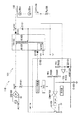
図1は、本発明の実施形態に係るLED駆動装置1及びこれを用いたLED照明装置10の構成を示す回路図である。本発明の実施形態に係るLED駆動装置1は、整流回路DBと、トランスTRと、第1のMOSFET(スイッチング素子)Q1と、ダイオードD1及びコンデンサC1から構成される整流平滑回路と、制御回路CNTと、コンデンサC3と、リプル電流低減回路3aと、を備える。LED駆動装置1とLED負荷2(LED1、・・・LEDn)とは、LED照明装置10を構成する。
(First embodiment)
FIG. 1 is a circuit diagram showing a configuration of an LED driving device 1 according to an embodiment of the present invention and an
整流回路DBは、周知のダイオードブリッジ回路であり、交流入力電源ACに接続され、交流入力電力を一方向の脈流に整流し、トランスTRに出力する。交流入力電源ACと整流回路DBとは、例えばバッテリ等の直流電源に置きかえられても良い。 The rectifier circuit DB is a well-known diode bridge circuit, is connected to the AC input power supply AC, rectifies AC input power into a unidirectional pulsating flow, and outputs it to the transformer TR. The AC input power source AC and the rectifier circuit DB may be replaced with a DC power source such as a battery.
トランスTRは、一次巻線W1と二次巻線W2と三次巻線W3とを有する。一次巻線W1の一端は、整流回路DBに接続され、一次巻線W1の他端は、第1のMOSFETQ1のドレイン端子に接続される。二次巻線W2の両端間には、ダイオードD1及びコンデンサC1から構成される整流平滑回路が接続される。三次巻線W3の両端間には、ダイオードD2及びコンデンサC2から構成される補助電源が接続される。 The transformer TR includes a primary winding W1, a secondary winding W2, and a tertiary winding W3. One end of the primary winding W1 is connected to the rectifier circuit DB, and the other end of the primary winding W1 is connected to the drain terminal of the first MOSFET Q1. A rectifying / smoothing circuit including a diode D1 and a capacitor C1 is connected between both ends of the secondary winding W2. An auxiliary power source composed of a diode D2 and a capacitor C2 is connected between both ends of the tertiary winding W3.
第1のMOSFETQ1のソース端子は接地され、ゲート端子は制御回路CNTに接続される。 The source terminal of the first MOSFET Q1 is grounded, and the gate terminal is connected to the control circuit CNT.
ダイオードD1及びコンデンサC1から構成される整流平滑回路の両端には、直列接続されたn個のLED素子(LED1、・・・LEDn)から構成されるLED負荷2とリプル電流低減回路3aとの直列回路が接続される。なお、nは1以上の自然数である。ダイオードD1のカソード端子とコンデンサC1の一端とは、LED負荷2を構成するLED素子LED1のアノード端子に接続される。コンデンサC1の他端は接地される。リプル電流低減回路3aは、リアクトルL1と電流検出抵抗Rsとが直列に接続されて構成される。
The
制御回路CNTの各端子は、第1のMOSFETQ1のゲート端子と、補助電源と、LED負荷2及び定電流制御回路3の接続点と、コンデンサC3と、に接続され、抵抗R1を介して整流回路DB及び一次巻線W1の接続点に接続される。制御回路CNTは、第1の誤差増幅器AMP1と、比較器CMPと、を備える。
Each terminal of the control circuit CNT is connected to the gate terminal of the first MOSFET Q1, the auxiliary power supply, the connection point of the
第1の誤差増幅器AMP1の反転入力端子は、LED負荷2及びリプル低減回路3aの接続点に接続され、非反転入力端子は定電流源REGとツェナーダイオードZD1とから構成される第1の基準電圧に接続される。第1の誤差増幅器AMP1の出力端子は、抵抗R3及びコンデンサC3から構成される積分回路を介して比較器CMPの第1の非反転入力端子に接続される。第1の誤差増幅器AMP1は、LED負荷2に流れる電流ILEDと第1の基準値(第1の基準電圧)とに基づく第1の誤差信号を、積分回路を介して比較器CMPに出力する。
The inverting input terminal of the first error amplifier AMP1 is connected to the connection point of the
比較器CMPの反転入力端子は、周知の三角波生成回路に接続され、第2の非反転入力端子は、定電流源REGと抵抗R4及びR5とから構成されるDUTY制限回路に接続される。比較器CMPの出力端子はドライバ回路を介して第1のMOSFETQ1のゲート端子に接続される。比較器CMPは、第1の誤差増幅器AMP1から出力される第1の誤差信号とDUTY制限回路の出力信号とのうち低レベルの信号と、三角波生成回路から出力される三角波と、に基づくPWM(パルス幅変調)信号をドライバ回路に出力する。即ち、詳細には、比較器CMPは、LED電流ILEDが第1の基準値よりも小さくなるとPWM信号のオンデューティを大きく(オン時間を長く)し、LED電流ILEDが第1の基準値よりも大きくなるとPWM信号のオンデューティを小さく(オン時間を短く)するように動作する。DUTY制限回路は、第1の誤差信号が大きくなりすぎたときにPWM信号のオンデューティの最大値を制限する。 The inverting input terminal of the comparator CMP is connected to a well-known triangular wave generating circuit, and the second non-inverting input terminal is connected to a DUTY limiting circuit including a constant current source REG and resistors R4 and R5. The output terminal of the comparator CMP is connected to the gate terminal of the first MOSFET Q1 through a driver circuit. The comparator CMP is a PWM (based on the low-level signal of the first error signal output from the first error amplifier AMP1 and the output signal of the DUTY limiting circuit, and the triangular wave output from the triangular wave generation circuit. (Pulse width modulation) signal is output to the driver circuit. Specifically, when the LED current I LED becomes smaller than the first reference value, the comparator CMP increases the on-duty of the PWM signal (lengthens the on-time), and the LED current I LED becomes the first reference value. When the value is larger than that, the PWM signal operates so as to reduce the ON duty of the PWM signal (shorten the ON time). The DUTY limiting circuit limits the maximum on-duty value of the PWM signal when the first error signal becomes too large.
第1の誤差信号は、上記の積分回路により積分され、比較器CMPの第1の非反転入力端子に入力される。従って、制御回路CNTの応答速度(応答周波数)は、抵抗R3及びコンデンサC3により決定される時定数に基づき、LED電流ILEDの変化よりも遅くなる。本実施形態に係るLED駆動装置1において、抵抗R3及びコンデンサC3の時定数は、第1の誤差信号が交流入力電源ACの1周期以上の期間にわたり積分されるように設定される。この場合、PWM信号のオンデューティは、交流入力電源ACの1周期において一定となるため、LED駆動装置1の力率が改善される。 The first error signal is integrated by the integration circuit and input to the first non-inverting input terminal of the comparator CMP. Therefore, the response speed (response frequency) of the control circuit CNT is slower than the change in the LED current I LED based on the time constant determined by the resistor R3 and the capacitor C3. In the LED drive device 1 according to this embodiment, the time constants of the resistor R3 and the capacitor C3 are set so that the first error signal is integrated over a period of one cycle or more of the AC input power supply AC. In this case, since the on-duty of the PWM signal is constant in one cycle of the AC input power supply AC, the power factor of the LED driving device 1 is improved.
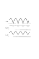
図2は、本発明の実施形態に係るLED駆動装置及びこれを用いたLED照明装置における各部の電圧及び電流の関係を示す波形図である。本発明の実施形態に係るLED駆動装置1において、制御回路CNTは、LED負荷2に流れる電流ILEDが第1の基準値(第1の基準電圧)になるように第1のMOSFETQ1をオンオフ制御する。即ち、LED駆動装置1は、従来のLED駆動装置と同様に交流入力電力を直流電力に変換してLED負荷2に供給する。そのため、出力電圧Vout(コンデンサC1の両端電圧)は、従来のLED駆動装置と同様に微小な電圧変動を含む。
FIG. 2 is a waveform diagram showing the relationship between the voltage and current of each part in the LED driving device according to the embodiment of the present invention and the LED lighting device using the LED driving device. In the LED drive device 1 according to the embodiment of the present invention, the control circuit CNT controls on / off of the first MOSFET Q1 so that the current I LED flowing through the
しかしながら、本発明の実施形態に係るLED駆動装置1において、出力電圧リプルにより出力電流リプルが発生しようとすると、リプル電流低減回路3aのリアクトルL1の両端に電圧が発生する。これにより、LED両端に発生する電圧リプルは軽減されるため、出力電流のリプルは低減される。
However, in the LED drive device 1 according to the embodiment of the present invention, when an output current ripple is generated by the output voltage ripple, a voltage is generated across the reactor L1 of the ripple
従って、従来のLED駆動装置において大きな電流変化を含んでいたLED電流ILEDは、本発明の実施形態に係るLED駆動装置1において、図2に示すように、電流リプルを低減するように制御される。 Therefore, the LED current I LED that includes a large current change in the conventional LED driving device is controlled to reduce current ripple in the LED driving device 1 according to the embodiment of the present invention, as shown in FIG. The
また、LED負荷2とリアクトルL1との接続点からフィードバック信号を取り出して、電力変換を制御するので、LED負荷2の順方向電圧VFのバラツキや温度特性による影響を小さくできる。従って、順方向電圧VFのバラツキや温度特性を考慮する必要がなくなる。
Further, since the feedback signal is taken out from the connection point between the
(第2の実施形態)
図3は、本発明の第2の実施形態に係るLED駆動装置及びこれを用いたLED照明装置の構成を示す回路図である。図3に示す第2の実施形態に係るLED駆動装置及びこれを用いたLED照明装置は、図1に示す第1の実施形態に係るLED駆動装置及びこれを用いたLED照明装置に対して、リプル電流低減回路3bのみが異なる。
(Second Embodiment)
FIG. 3 is a circuit diagram showing a configuration of an LED driving device and an LED lighting device using the same according to the second embodiment of the present invention. The LED driving device according to the second embodiment shown in FIG. 3 and the LED lighting device using the LED driving device according to the second embodiment are compared with the LED driving device according to the first embodiment shown in FIG. 1 and the LED lighting device using the LED driving device. Only the ripple
リプル電流低減回路3bは、ダイオードD1及びコンデンサC1から構成される整流平滑回路とLED負荷2と制御回路CNTとに接続される。リプル電流低減回路3bは、本発明のフィードバック型定電流制御回路に対応し、第2のMOSFET(可変インピーダンス素子)Q2と検出抵抗(電流検出部)Rsと第2の誤差増幅器AMP2とツェナーダイオードZD2とを備える。第2のMOSFETQ2のドレイン端子はLED素子LEDnのカソード端子に接続され、ソース端子は検出抵抗Rsを介して接地され、ゲート端子は第2の誤差増幅器AMP2の出力端子に接続される。第2のMOSFETQ2は、第2の誤差増幅器AMP2の出力に応じてドレイン・ソース間の抵抗値を連続的に変化させる。従って、第2のMOSFETQ2は、電気信号により抵抗値が変化する周知の可変抵抗素子と置きかえることができる。リプル電流低減回路3bの応答速度は、制御回路CNTの応答速度よりも高く設定され、好ましくは交流入力電源ACの周波数よりも高く設定される。
The ripple
検出抵抗Rsと第2のMOSFETQ2のソース端子との接続点は、第2の誤差増幅器AMP2の反転入力端子に接続される。検出抵抗Rsは、LED負荷2に流れる電流ILEDを電圧信号に変換して第2の誤差増幅器AMP2に出力する。検出抵抗Rsは、これ以外の電流検出手段、例えばカレントトランスに置きかえられても良く、LED電流ILEDを電圧以外の電気信号によって出力できる構成に置きかえられても良い。
A connection point between the detection resistor Rs and the source terminal of the second MOSFET Q2 is connected to the inverting input terminal of the second error amplifier AMP2. The detection resistor Rs converts the current I LED flowing through the
ツェナーダイオードZD2のカソード端子は、抵抗R6を介してダイオードD1及びコンデンサC1の接続点に接続され、且つ、第2の誤差増幅器AMP2の非反転入力端子に接続される。ツェナーダイオードZD2のアノード端子は、接地される。 The cathode terminal of the Zener diode ZD2 is connected to the connection point of the diode D1 and the capacitor C1 via the resistor R6, and is connected to the non-inverting input terminal of the second error amplifier AMP2. The anode terminal of the Zener diode ZD2 is grounded.
第2の誤差増幅器AMP2の非反転入力端子は、ツェナーダイオードZD2を含んで構成される第2の基準電圧に接続される。第2の誤差増幅器AMP2の出力端子は、第2のMOSFETQ2のゲート端子に接続される。第2の誤差増幅器AMP2は、LED負荷2に流れる電流ILEDと第2の基準値(第2の基準電圧)とに基づく第2の誤差信号を第2のMOSFETQ2に出力する。詳細には、第2の誤差増幅器AMP2は、LED電流ILEDが第2の基準値よりも小さくなるほど第2の誤差信号の電圧レベルを大きくし、第2のMOSFETのソース・ドレイン間の抵抗値を低くする。また、第2の誤差増幅器AMP2は、LED電流ILEDが第2の基準値よりも大きくなるほど第2の誤差信号の電圧レベルを小さくし、第2のMOSFETのソース・ドレイン間の抵抗値を高くするように動作する。
The non-inverting input terminal of the second error amplifier AMP2 is connected to a second reference voltage that includes the Zener diode ZD2. The output terminal of the second error amplifier AMP2 is connected to the gate terminal of the second MOSFET Q2. The second error amplifier AMP2 outputs a second error signal based on the current I LED flowing through the
本発明の実施形態に係るLED駆動装置1において、制御回路CNTは、LED負荷2に流れる電流ILEDが第1の基準値(第1の基準電圧)になるように第1のMOSFETQ1をオンオフ制御する。即ち、LED駆動装置1は、従来のLED駆動装置と同様に交流入力電力を直流電力に変換してLED負荷2に供給する。そのため、出力電圧Vout(コンデンサC1の両端電圧)は、従来のLED駆動装置と同様に微小な電圧変動を含む。
In the LED drive device 1 according to the embodiment of the present invention, the control circuit CNT controls on / off of the first MOSFET Q1 so that the current I LED flowing through the
しかしながら、本発明の実施形態に係るLED駆動装置1において、リプル電流低減回路3bは、LED電流ILEDに基づく第2の誤差信号が第2の基準値(第2の基準電圧)になるように第2のMOSFETQ2を制御する。従って、従来のLED駆動装置において大きな電流変化を含んでいたLED電流ILEDは、本発明の実施形態に係るLED駆動装置1において、電流リプルを低減するように制御される。
However, in the LED drive device 1 according to the embodiment of the present invention, the ripple
従って、本発明の実施形態に係るLED駆動装置は、以下の作用効果を有する。 (1)リプル電流低減回路3bは、力率改善動作を行う必要が無いため、制御の応答速度(応答周波数)を制御回路CNTよりも早く設定することができ、LED負荷2を流れるLED電流ILEDに含まれる電流リプルを低減することができる。
Therefore, the LED driving device according to the embodiment of the present invention has the following effects. (1) Since the ripple
(2)また、LED負荷2とリアクトルL1との接続点からフィードバック信号を取り出して、電力変換を制御するので、LED負荷2の順方向電圧VFのバラツキや温度特性による影響を小さくできる。従って、順方向電圧VFのバラツキや温度特性を考慮する必要がなくなる。
(2) Moreover, since a feedback signal is taken out from the connection point between the
(3)LED負荷2に流れる電流ILEDに発生するリプルを低減することができるため
、LED負荷2の発光を安定化できる。
(3) it is possible to reduce the ripple occurring in the current I LED flowing through the
(4)大型の電解コンデンサや交流/直流変換器を用いることなくLED負荷2の発光を安定化できるので、LED駆動装置を簡易な回路で小型且つ安価に構成することができる。
(4) Since the light emission of the
(5)LED負荷2を流れるLED電流ILEDの変化が小さくなるため、LED照明装
置10から放出されるノイズが低減される。
(5) Since the change in the LED current I LED flowing through the
(6)LED電流ILEDの変化が小さくなるため、LED負荷2を構成するLED素子
(LED1、・・・LEDn)に大きなピーク電流が流れにくくなる。これにより、LED素子(LED1、・・・LEDn)にかかる電気的ストレスが低減され、LED負荷2の長寿命化が達成される。
(6) LED current I Since the change in LED is small, it is difficult for a large peak current to flow through the LED elements (LED1,... LEDn) constituting the
(7)出力電圧Voutの電圧リプルは微小なものであるから、第2のMOSFET及び
検出抵抗による消費電力は比較的小さく、LED駆動装置の高効率化が達成される。
(7) Since the voltage ripple of the output voltage V out is very small, the power consumption by the second MOSFET and the detection resistor is relatively small, and high efficiency of the LED driving device is achieved.
以上の実施形態で説明された構成、形状、大きさおよび配置関係については、本発明が理解・実施できる程度に概略的に示したものにすぎない。従って本発明は、説明された実施形態に限定されるものではなく、特許請求の範囲に示される技術的思想の範囲を逸脱しない限り様々な形態に変更することができる。 The configurations, shapes, sizes, and arrangement relationships described in the above embodiments are merely schematically shown to the extent that the present invention can be understood and implemented. Therefore, the present invention is not limited to the described embodiments, and can be variously modified without departing from the scope of the technical idea shown in the claims.
例えば、本発明の実施形態にかかるLED駆動装置は、トランスを介した回路構成を有するが、トランスの有無や絶縁/非絶縁などの回路構成はこれに限定されるものではない。 For example, the LED drive device according to the embodiment of the present invention has a circuit configuration via a transformer, but the circuit configuration such as the presence or absence of the transformer and insulation / non-insulation is not limited to this.
また、制御回路CNTの応答速度は、上述の積分回路に限らず制御回路CNTに含まれる構成で決定することができる。また、第1の基準値及び第2の基準値を外部信号等により可変させるようにしても良い。 Further, the response speed of the control circuit CNT can be determined by the configuration included in the control circuit CNT as well as the integration circuit described above. Further, the first reference value and the second reference value may be varied by an external signal or the like.
1 LED駆動装置
2 LED負荷
3 定電流制御回路
10 LED照明装置
AMP 誤差増幅器
CMP 比較器
Q1,Q2 MOSFET
Rs 検出抵抗
ZD ツェナーダイオード
L リアクトル
DESCRIPTION OF SYMBOLS 1
Rs detection resistor ZD Zener diode L reactor
Claims (8)
オンオフ制御されるスイッチング素子と、
前記LED負荷に直列に接続され、前記LED負荷に流れる電流リプルを低減するリプル電流低減部と、
前記LED負荷と前記リプル電流低減部との接続点におけるフィードバック電圧に基づき前記スイッチング素子をオンオフ制御することにより前記直流出力電力を所定値に制御する制御回路と、
を備えることを特徴とするLED駆動装置。 An LED drive device that converts alternating current input power into desired direct current output power and supplies it to an LED load,
A switching element controlled on and off;
A ripple current reduction unit that is connected in series to the LED load and reduces a current ripple flowing in the LED load;
A control circuit for controlling the DC output power to a predetermined value by on / off controlling the switching element based on a feedback voltage at a connection point between the LED load and the ripple current reducing unit;
An LED driving device comprising:
An LED lighting device comprising the LED driving device according to any one of claims 1 to 7.
Priority Applications (5)
| Application Number | Priority Date | Filing Date | Title |
|---|---|---|---|
| JP2011239939A JP5110197B2 (en) | 2011-01-18 | 2011-11-01 | LED driving device and LED lighting device |
| KR20110142039A KR101302993B1 (en) | 2011-01-18 | 2011-12-26 | Led driving device and led lighting device |
| US13/348,068 US9113519B2 (en) | 2011-01-18 | 2012-01-11 | LED driving apparatus and LED lighting apparatus |
| TW101101906A TWI468076B (en) | 2011-01-18 | 2012-01-18 | LED driver and LED lighting device |
| CN201210016851.6A CN102612206B (en) | 2011-01-18 | 2012-01-18 | LED driving apparatus and LED lighting apparatus |
Applications Claiming Priority (3)
| Application Number | Priority Date | Filing Date | Title |
|---|---|---|---|
| JP2011007427 | 2011-01-18 | ||
| JP2011007427 | 2011-01-18 | ||
| JP2011239939A JP5110197B2 (en) | 2011-01-18 | 2011-11-01 | LED driving device and LED lighting device |
Related Child Applications (1)
| Application Number | Title | Priority Date | Filing Date |
|---|---|---|---|
| JP2012182968A Division JP2012227171A (en) | 2011-01-18 | 2012-08-22 | Led driving device and led lighting apparatus |
Publications (2)
| Publication Number | Publication Date |
|---|---|
| JP2012164633A true JP2012164633A (en) | 2012-08-30 |
| JP5110197B2 JP5110197B2 (en) | 2012-12-26 |
Family
ID=46490280
Family Applications (1)
| Application Number | Title | Priority Date | Filing Date |
|---|---|---|---|
| JP2011239939A Active JP5110197B2 (en) | 2011-01-18 | 2011-11-01 | LED driving device and LED lighting device |
Country Status (5)
| Country | Link |
|---|---|
| US (1) | US9113519B2 (en) |
| JP (1) | JP5110197B2 (en) |
| KR (1) | KR101302993B1 (en) |
| CN (1) | CN102612206B (en) |
| TW (1) | TWI468076B (en) |
Cited By (9)
| Publication number | Priority date | Publication date | Assignee | Title |
|---|---|---|---|---|
| JP2017503351A (en) * | 2014-01-06 | 2017-01-26 | フィリップス ライティング ホールディング ビー ヴィ | LED drive based on ripple |
| JP2017533558A (en) * | 2014-11-03 | 2017-11-09 | フィリップス ライティング ホールディング ビー ヴィ | Linear post regulator |
| JP2020180943A (en) * | 2019-04-26 | 2020-11-05 | 日亜化学工業株式会社 | Light-emitting diode inspection device |
| JP2020198752A (en) * | 2019-06-05 | 2020-12-10 | ミツミ電機株式会社 | Power source device, semiconductor integrated circuit, and ripple suppressing method |
| JP2021048760A (en) * | 2019-09-20 | 2021-03-25 | 東芝ライテック株式会社 | Power supply device and illumination device |
| JP2022030037A (en) * | 2020-08-06 | 2022-02-18 | サンケン電気株式会社 | Switching power supply device |
| US11956870B2 (en) | 2019-12-18 | 2024-04-09 | Nichia Corporation | Light-source device |
| JP7484522B2 (en) | 2020-07-16 | 2024-05-16 | 三菱電機株式会社 | Lighting fixture, connection unit and lighting device |
| JP7501212B2 (en) | 2020-08-06 | 2024-06-18 | サンケン電気株式会社 | Switching Power Supply Unit |
Families Citing this family (17)
| Publication number | Priority date | Publication date | Assignee | Title |
|---|---|---|---|---|
| KR101187189B1 (en) * | 2012-03-07 | 2012-10-02 | 유상우 | Led driving circuit having function of efficiency improvement |
| CN103096599B (en) * | 2013-01-18 | 2015-05-20 | 深圳市华星光电技术有限公司 | Device and method of light emitting diode (LED) dimming driving |
| JP2014160574A (en) * | 2013-02-20 | 2014-09-04 | Sanken Electric Co Ltd | Led driving device and led lighting device |
| US9049760B2 (en) * | 2013-03-11 | 2015-06-02 | Immense Advance Technology Corp. | PFC LED driver having a flicker control mechanism |
| KR101292219B1 (en) | 2013-05-27 | 2013-08-02 | 주식회사엘이디파워 | Power supply apparatus of led lamp for ripple remove device |
| CN103269550B (en) * | 2013-06-04 | 2015-02-04 | 上海晶丰明源半导体有限公司 | LED ((Light Emitting Diode) current ripple elimination driving circuit |
| TWM467016U (en) * | 2013-06-27 | 2013-12-01 | Yu-Lin Lee | Hybrid constant current led lamp |
| CN203675400U (en) * | 2013-12-27 | 2014-06-25 | 陈俞好 | LED drive device, battery charger and drive control circuit thereof |
| KR101641131B1 (en) * | 2014-03-14 | 2016-07-21 | 한국광기술원 | Multi-channel circuit for removing flicker |
| CN104485634B (en) * | 2014-12-16 | 2018-05-01 | 上海数明半导体有限公司 | Realize the power-supply management system and method for average current protection |
| KR101674549B1 (en) * | 2015-12-30 | 2016-11-22 | 지홈엘이디 주식회사 | power ripple elimination device of LED lamp |
| KR101674550B1 (en) * | 2015-12-30 | 2016-11-22 | 지홈엘이디 주식회사 | dimming control device of LED lamp using switch on-off signal |
| US9900938B2 (en) | 2016-01-26 | 2018-02-20 | Fairchild Korea Semiconductor Ltd. | LED lighting circuit with ripple reducer |
| KR101651507B1 (en) * | 2016-04-29 | 2016-09-05 | 주식회사 엘이디파워 | Dimming Type LED Lighting Device Using Switching On/Off Signals |
| WO2017188757A2 (en) * | 2016-04-29 | 2017-11-02 | 주식회사 엘이디파워 | Dimming-type led lighting apparatus having electrolytic capacitor-less power supply device |
| KR101651508B1 (en) * | 2016-04-29 | 2016-09-05 | 주식회사 엘이디파워 | Dimming Type LED Lighting Device Including Element for providing Power with Electrolysis Capacitor-less |
| US10050517B1 (en) | 2017-01-31 | 2018-08-14 | Ricoh Electronics Devices Co., Ltd. | Power supply apparatus converting input voltage to predetermined output voltage and controlling output voltage based on feedback signal corresponding to output voltage |
Citations (3)
| Publication number | Priority date | Publication date | Assignee | Title |
|---|---|---|---|---|
| JP2001313423A (en) * | 2000-04-28 | 2001-11-09 | Toshiba Lighting & Technology Corp | Light-emitting diode drive device |
| JP2004327152A (en) * | 2003-04-23 | 2004-11-18 | Toshiba Lighting & Technology Corp | Led lighting device and led lighting fixture |
| JP2007194478A (en) * | 2006-01-20 | 2007-08-02 | Matsushita Electric Ind Co Ltd | Light-emitting diode driving device |
Family Cites Families (17)
| Publication number | Priority date | Publication date | Assignee | Title |
|---|---|---|---|---|
| US6577512B2 (en) | 2001-05-25 | 2003-06-10 | Koninklijke Philips Electronics N.V. | Power supply for LEDs |
| US20080018261A1 (en) * | 2006-05-01 | 2008-01-24 | Kastner Mark A | LED power supply with options for dimming |
| KR101255276B1 (en) * | 2006-09-12 | 2013-04-15 | 엘지디스플레이 주식회사 | Back light unit and liquid crystal display device using the same |
| JP5089193B2 (en) | 2007-02-22 | 2012-12-05 | 株式会社小糸製作所 | Light emitting device |
| US7750616B2 (en) | 2007-06-21 | 2010-07-06 | Green Mark Technology Inc. | Buck converter LED driver circuit |
| TWI400989B (en) * | 2008-05-30 | 2013-07-01 | Green Solution Technology Inc | Light emitting diode driving circuit and controller thereof |
| US8653757B2 (en) * | 2008-06-04 | 2014-02-18 | Nxp B.V. | DC-DC converter |
| US7999487B2 (en) * | 2008-06-10 | 2011-08-16 | Allegro Microsystems, Inc. | Electronic circuit for driving a diode load with a predetermined average current |
| US8665922B2 (en) | 2008-10-31 | 2014-03-04 | Sanyo Electric Co., Ltd. | Driver circuit of light-emitting element |
| US8044609B2 (en) * | 2008-12-31 | 2011-10-25 | 02Micro Inc | Circuits and methods for controlling LCD backlights |
| JP4630930B2 (en) | 2009-01-29 | 2011-02-09 | 極光電気株式会社 | LED driving circuit and LED lighting device using the same |
| JP5225135B2 (en) | 2009-02-10 | 2013-07-03 | 三菱電機株式会社 | Power supply circuit and lighting device |
| CN101827476A (en) | 2009-03-04 | 2010-09-08 | 立锜科技股份有限公司 | Led drive circuit and correlation technique and integrated circuit with the direct conversion and control function of alternating current-direct current |
| CN101674693B (en) | 2009-10-01 | 2012-07-18 | 英飞特电子(杭州)有限公司 | Multichannel constant-current control circuit applicable to LED driver |
| KR100946685B1 (en) | 2009-10-20 | 2010-03-12 | 주식회사 동운아나텍 | Light emitting diode driving apparatus |
| US8294379B2 (en) | 2009-11-10 | 2012-10-23 | Green Mark Technology Inc. | Dimmable LED lamp and dimmable LED lighting apparatus |
| KR101566200B1 (en) * | 2009-12-09 | 2015-11-05 | 삼성전자 주식회사 | Display device and driving method thereof |
-
2011
- 2011-11-01 JP JP2011239939A patent/JP5110197B2/en active Active
- 2011-12-26 KR KR20110142039A patent/KR101302993B1/en active IP Right Grant
-
2012
- 2012-01-11 US US13/348,068 patent/US9113519B2/en active Active
- 2012-01-18 TW TW101101906A patent/TWI468076B/en not_active IP Right Cessation
- 2012-01-18 CN CN201210016851.6A patent/CN102612206B/en active Active
Patent Citations (3)
| Publication number | Priority date | Publication date | Assignee | Title |
|---|---|---|---|---|
| JP2001313423A (en) * | 2000-04-28 | 2001-11-09 | Toshiba Lighting & Technology Corp | Light-emitting diode drive device |
| JP2004327152A (en) * | 2003-04-23 | 2004-11-18 | Toshiba Lighting & Technology Corp | Led lighting device and led lighting fixture |
| JP2007194478A (en) * | 2006-01-20 | 2007-08-02 | Matsushita Electric Ind Co Ltd | Light-emitting diode driving device |
Cited By (13)
| Publication number | Priority date | Publication date | Assignee | Title |
|---|---|---|---|---|
| JP2017503351A (en) * | 2014-01-06 | 2017-01-26 | フィリップス ライティング ホールディング ビー ヴィ | LED drive based on ripple |
| JP2017533558A (en) * | 2014-11-03 | 2017-11-09 | フィリップス ライティング ホールディング ビー ヴィ | Linear post regulator |
| JP7467030B2 (en) | 2019-04-26 | 2024-04-15 | 日亜化学工業株式会社 | Light emitting diode inspection equipment |
| JP2020180943A (en) * | 2019-04-26 | 2020-11-05 | 日亜化学工業株式会社 | Light-emitting diode inspection device |
| JP2020198752A (en) * | 2019-06-05 | 2020-12-10 | ミツミ電機株式会社 | Power source device, semiconductor integrated circuit, and ripple suppressing method |
| JP7256384B2 (en) | 2019-06-05 | 2023-04-12 | ミツミ電機株式会社 | Power supply device, semiconductor integrated circuit and ripple suppression method |
| JP7303488B2 (en) | 2019-09-20 | 2023-07-05 | 東芝ライテック株式会社 | Power supply and lighting system |
| JP2021048760A (en) * | 2019-09-20 | 2021-03-25 | 東芝ライテック株式会社 | Power supply device and illumination device |
| US11956870B2 (en) | 2019-12-18 | 2024-04-09 | Nichia Corporation | Light-source device |
| JP7484522B2 (en) | 2020-07-16 | 2024-05-16 | 三菱電機株式会社 | Lighting fixture, connection unit and lighting device |
| JP2022030037A (en) * | 2020-08-06 | 2022-02-18 | サンケン電気株式会社 | Switching power supply device |
| JP7498060B2 (en) | 2020-08-06 | 2024-06-11 | サンケン電気株式会社 | Switching Power Supply Unit |
| JP7501212B2 (en) | 2020-08-06 | 2024-06-18 | サンケン電気株式会社 | Switching Power Supply Unit |
Also Published As
| Publication number | Publication date |
|---|---|
| TW201233248A (en) | 2012-08-01 |
| TWI468076B (en) | 2015-01-01 |
| CN102612206A (en) | 2012-07-25 |
| US20120181941A1 (en) | 2012-07-19 |
| JP5110197B2 (en) | 2012-12-26 |
| CN102612206B (en) | 2015-07-15 |
| KR20120083845A (en) | 2012-07-26 |
| KR101302993B1 (en) | 2013-09-03 |
| US9113519B2 (en) | 2015-08-18 |
Similar Documents
| Publication | Publication Date | Title |
|---|---|---|
| JP5110197B2 (en) | LED driving device and LED lighting device | |
| JP5564239B2 (en) | LED drive circuit | |
| TWI566637B (en) | A cascade boost and inverting buck converter with independent control | |
| TWI404452B (en) | Current supply circuit and current control circuit for led | |
| JP2014160574A (en) | Led driving device and led lighting device | |
| JP2011065980A (en) | System and method in order to drive light source | |
| JP2010040878A (en) | Lighting device for light-emitting diode | |
| Chung et al. | Low-cost drive circuit for AC-direct LED lamps | |
| JP6108143B2 (en) | Overcurrent prevention type power supply device and lighting fixture using the same | |
| JP5528883B2 (en) | LED drive circuit | |
| US9999104B2 (en) | Lighting device and luminaire | |
| JP2015018638A (en) | Lighting device | |
| JP6534060B2 (en) | Lighting device and lighting apparatus | |
| JP6417930B2 (en) | Non-insulated power supply | |
| JP6840997B2 (en) | Lighting equipment and lighting equipment | |
| TWI595802B (en) | Dimming module, dimming method and lighting device | |
| JP5551995B2 (en) | Power supply device and lighting device provided with the power supply device | |
| JP2012227171A (en) | Led driving device and led lighting apparatus | |
| JP2017107777A (en) | Lighting device and luminaire having the same | |
| WO2013172259A1 (en) | Switching power supply circuit and led lighting device | |
| JP6485770B2 (en) | Lighting device and lighting apparatus | |
| TW201438518A (en) | LED dimming control device | |
| JP2014102950A (en) | Solid-state light-emitting element drive device, illuminating device, and illuminating fixture | |
| JP7082902B2 (en) | Load drive | |
| JP2017059500A (en) | Lighting appliance |
Legal Events
| Date | Code | Title | Description |
|---|---|---|---|
| A131 | Notification of reasons for refusal |
Free format text: JAPANESE INTERMEDIATE CODE: A131 Effective date: 20120703 |
|
| A521 | Request for written amendment filed |
Free format text: JAPANESE INTERMEDIATE CODE: A523 Effective date: 20120822 |
|
| TRDD | Decision of grant or rejection written | ||
| A01 | Written decision to grant a patent or to grant a registration (utility model) |
Free format text: JAPANESE INTERMEDIATE CODE: A01 Effective date: 20120911 |
|
| A01 | Written decision to grant a patent or to grant a registration (utility model) |
Free format text: JAPANESE INTERMEDIATE CODE: A01 |
|
| A621 | Written request for application examination |
Free format text: JAPANESE INTERMEDIATE CODE: A621 Effective date: 20121001 |
|
| A61 | First payment of annual fees (during grant procedure) |
Free format text: JAPANESE INTERMEDIATE CODE: A61 Effective date: 20120924 |
|
| FPAY | Renewal fee payment (event date is renewal date of database) |
Free format text: PAYMENT UNTIL: 20151019 Year of fee payment: 3 |
|
| R150 | Certificate of patent or registration of utility model |
Ref document number: 5110197 Country of ref document: JP Free format text: JAPANESE INTERMEDIATE CODE: R150 Free format text: JAPANESE INTERMEDIATE CODE: R150 |
|
| R250 | Receipt of annual fees |
Free format text: JAPANESE INTERMEDIATE CODE: R250 |
|
| R250 | Receipt of annual fees |
Free format text: JAPANESE INTERMEDIATE CODE: R250 |
|
| R250 | Receipt of annual fees |
Free format text: JAPANESE INTERMEDIATE CODE: R250 |
|
| R250 | Receipt of annual fees |
Free format text: JAPANESE INTERMEDIATE CODE: R250 |
|
| R250 | Receipt of annual fees |
Free format text: JAPANESE INTERMEDIATE CODE: R250 |
|
| R250 | Receipt of annual fees |
Free format text: JAPANESE INTERMEDIATE CODE: R250 |
|
| R250 | Receipt of annual fees |
Free format text: JAPANESE INTERMEDIATE CODE: R250 |
|
| R250 | Receipt of annual fees |
Free format text: JAPANESE INTERMEDIATE CODE: R250 |
|
| R250 | Receipt of annual fees |
Free format text: JAPANESE INTERMEDIATE CODE: R250 |