JP2012162680A - Adhesive film for semiconductor, adhesive sheet, semiconductor wafer, and semiconductor device - Google Patents
Adhesive film for semiconductor, adhesive sheet, semiconductor wafer, and semiconductor device Download PDFInfo
- Publication number
- JP2012162680A JP2012162680A JP2011025403A JP2011025403A JP2012162680A JP 2012162680 A JP2012162680 A JP 2012162680A JP 2011025403 A JP2011025403 A JP 2011025403A JP 2011025403 A JP2011025403 A JP 2011025403A JP 2012162680 A JP2012162680 A JP 2012162680A
- Authority
- JP
- Japan
- Prior art keywords
- semiconductor
- adhesive
- resin
- adhesive film
- adhesive layer
- Prior art date
- Legal status (The legal status is an assumption and is not a legal conclusion. Google has not performed a legal analysis and makes no representation as to the accuracy of the status listed.)
- Granted
Links
- FQYUMYWMJTYZTK-UHFFFAOYSA-N C(C1OC1)Oc1ccccc1 Chemical compound C(C1OC1)Oc1ccccc1 FQYUMYWMJTYZTK-UHFFFAOYSA-N 0.000 description 2
- 0 CC(C)(C)*(c1cc(OCC2OC2)ccc1)I Chemical compound CC(C)(C)*(c1cc(OCC2OC2)ccc1)I 0.000 description 2
Images

Abstract
Description
本発明は、半導体用接着フィルム、それを用いた接着シート、半導体ウエハ及び半導体装置に関する。 The present invention relates to an adhesive film for a semiconductor, an adhesive sheet using the same, a semiconductor wafer, and a semiconductor device.
従来、半導体素子と半導体素子搭載用支持部材の接合には、銀ペーストが主に使用されていた。しかしながら、近年の半導体素子の大型化、半導体パッケージの小型化・高性能化に伴い、使用される支持部材にも小型化、細密化が要求されるようになってきている。 Conventionally, a silver paste has been mainly used for joining a semiconductor element and a semiconductor element mounting support member. However, with the recent increase in the size of semiconductor elements and the reduction in size and performance of semiconductor packages, the support members used are also required to be reduced in size and density.
こうした要求に対して、銀ペーストでは、ぬれ広がり性、はみ出しや半導体素子の傾きに起因して発生するワイヤボンディング時の不具合、銀ペーストの厚み制御の困難、及び銀ペーストのボイド発生などにより、前記要求に対処しきれなくなってきている。そのため、前記要求に対処するべく、近年、フィルム状の接着剤が使用されるようになってきた(例えば、特許文献1、特許文献2参照)。
In response to such demands, the silver paste has the above-described wettability, defects due to wire bonding caused by protrusion and inclination of the semiconductor element, difficulty in controlling the thickness of the silver paste, and voids in the silver paste. It is becoming impossible to meet the demand. For this reason, in order to cope with the above demand, in recent years, a film-like adhesive has been used (see, for example,
この半導体用接着フィルムは、個片貼付け方式あるいはウエハ裏面貼付方式において使用されている。前者の個片貼付け方式の半導体用接着フィルムを用いて半導体装置を製造する場合、まず、リール状の半導体用接着フィルムをカッティングあるいはパンチングによって個片に切り出した後、支持部材に接着し、前記半導体用接着フィルム付き支持部材に、ダイシング工程によって個片化された半導体素子を接合して、半導体素子付き支持部材を作製する。その後、ワイヤボンド工程、封止工程などを経ることによって半導体装置が得られる(例えば、特許文献3参照)。しかし、前記個片貼付け方式の半導体用接着フィルムを用いるためには、半導体用接着フィルムを切り出して支持部材に接着する専用の組立装置が必要であることから、銀ペーストを使用する方法に比べて製造コストが高くなるという問題があった。 This adhesive film for semiconductors is used in an individual piece attaching method or a wafer back surface attaching method. When a semiconductor device is manufactured using the former adhesive film for semiconductors of the individual piece pasting method, first, a reel-like adhesive film for semiconductor is cut into individual pieces by cutting or punching, and then adhered to a support member, and the semiconductor The semiconductor element separated by the dicing process is joined to the supporting member with the adhesive film for manufacturing to produce the supporting member with the semiconductor element. Thereafter, a semiconductor device is obtained through a wire bonding process, a sealing process, and the like (see, for example, Patent Document 3). However, in order to use the adhesive film for semiconductors of the above-mentioned individual pasting method, a dedicated assembly device that cuts out the adhesive film for semiconductor and adheres it to the support member is required, compared with the method using silver paste. There was a problem that the manufacturing cost was high.
一方、ウエハ裏面貼付け方式の半導体用接着フィルムを用いて半導体装置を製造する場合、まず半導体ウエハの裏面に半導体用接着フィルムの一方の面を貼付け、さらに半導体用接着フィルムの他面にダイシングシートを貼り合わせる。その後、前記ウエハからダイシングによって半導体素子を個片化し、個片化した半導体用接着フィルム付き半導体素子をピックアップし、それを支持部材に接合し、その後のワイヤボンド、封止などの工程を経ることにより、半導体装置が得られる。このウエハ裏面貼付け方式の半導体用接着フィルムは、半導体用接着フィルム付き半導体素子を支持部材に接合するため、半導体用接着フィルムを個片化する装置を必要とせず、従来の銀ペースト用の組立装置をそのまま、あるいは熱盤を付加するなどの装置の一部を改良することにより使用できる。そのため、半導体用接着フィルムを用いた組立方法の中で製造コストが比較的安く抑えられる方法として注目されている(例えば、特許文献4参照)。 On the other hand, when manufacturing a semiconductor device using an adhesive film for semiconductor of a wafer back surface pasting method, first, one surface of the adhesive film for semiconductor is pasted on the back surface of the semiconductor wafer, and further a dicing sheet is attached to the other surface of the adhesive film for semiconductor. to paste together. Thereafter, the semiconductor element is separated into pieces from the wafer by dicing, and the separated semiconductor element with an adhesive film for a semiconductor is picked up and bonded to a support member, followed by steps such as wire bonding and sealing. Thus, a semiconductor device is obtained. The adhesive film for semiconductor of this wafer back surface pasting method does not require a device for separating the adhesive film for semiconductor, because the semiconductor element with the adhesive film for semiconductor is bonded to the support member, and is a conventional assembly device for silver paste Can be used by modifying a part of the apparatus as it is or by adding a hot platen. Therefore, it has been attracting attention as a method in which the manufacturing cost can be kept relatively low among the assembling methods using the adhesive film for semiconductor (see, for example, Patent Document 4).
しかし、最近になって、半導体素子の小型薄型化・高性能化に加えて、多機能化が進み、それに伴って複数の半導体素子を積層化した半導体装置が急増している。一方で前記の半導体装置の厚みは薄化の方向に進むことから、半導体用接着フィルムについてもさらなる極薄化が進んでいる。それに伴い、フィルム形成時のピンホールやはじきなどによる歩留まりの低下が大きな課題となっている。このような課題を解決するため、離型処理剤を有していない高表面エネルギー基材を用いると、フィルムが基材からはく離しにくくなるといった問題が発生する。また、熱可塑性樹脂を高分子量化して塗工ワニス粘度を上昇させると、薄膜塗工が困難となったり、得られたフィルムの熱時流動性が損なわれるといった問題が発生する。 However, recently, in addition to the downsizing, thinning, and high performance of semiconductor elements, the number of semiconductor devices in which a plurality of semiconductor elements are stacked is rapidly increasing along with the progress of multifunction. On the other hand, since the thickness of the semiconductor device proceeds in the direction of thinning, the thickness of the adhesive film for semiconductor is further reduced. Along with this, a decrease in yield due to pinholes and repelling during film formation has become a major issue. In order to solve such a problem, when a high surface energy base material having no release treatment agent is used, there arises a problem that the film is difficult to peel off from the base material. Moreover, when the thermoplastic resin is made to have a high molecular weight to increase the viscosity of the coating varnish, there are problems that thin film coating becomes difficult and the fluidity during heating of the obtained film is impaired.
そのため、薄膜形成が可能で、製造工程での歩留が向上し製造コストの軽減が図られる接着フィルムが強く求められていた。 Therefore, there has been a strong demand for an adhesive film capable of forming a thin film, improving yield in the manufacturing process, and reducing manufacturing cost.
本発明は、上記した従来技術の問題に鑑み、良好な薄膜塗工性(フィルム形成性)と基材からの軽はく離性が両立でき、さらに半導体素子と支持部材もしくは半導体素子同士を接合する際には高温接着性に優れる半導体用接着フィルム、当該半導体用接着フィルムを用いた接着シート、当該半導体用接着フィルム又は接着シートを用いた半導体ウエハ、及び当該半導体用接着フィルムを用いた半導体装置を提供することを目的とする。 In view of the above-mentioned problems of the prior art, the present invention can achieve both good thin film coatability (film formability) and light peelability from a substrate, and further when a semiconductor element and a support member or semiconductor elements are joined together. Provides a semiconductor adhesive film excellent in high-temperature adhesiveness, an adhesive sheet using the semiconductor adhesive film, a semiconductor wafer using the semiconductor adhesive film or adhesive sheet, and a semiconductor device using the semiconductor adhesive film The purpose is to do.
本発明者らは、上記課題を解決すべく鋭意検討した結果、以下の解決手段を提供するに至った。 As a result of intensive studies to solve the above problems, the present inventors have provided the following means for solving the problems.
本発明の半導体用接着フィルムは、基材(1)と、(A)熱可塑性樹脂及び(B)熱硬化性樹脂を含有し、表面自由エネルギーが15〜25mN/mであり、膜厚が10μm以下であり、基材に積層された接着剤層(2)と、を備え、基材(1)と接着剤層(2)とのピール剥離強度(X)が1〜50mN/cmである。 The adhesive film for a semiconductor of the present invention contains a base material (1), (A) a thermoplastic resin and (B) a thermosetting resin, has a surface free energy of 15 to 25 mN / m, and a film thickness of 10 μm. The adhesive layer (2) laminated on the substrate is provided, and the peel peel strength (X) between the substrate (1) and the adhesive layer (2) is 1 to 50 mN / cm.
「表面自由エネルギー」は、例えば、水、グリセリン及びホルムアミドをプローブ液体としてその測定対象面に対する接触角を測定し、DropMaster 500(協和界面科学社製)に搭載の解析ソフト(FAMAS)を用いて酸−塩基法により求めればよい。 “Surface free energy” is obtained by measuring the contact angle with respect to the surface to be measured using, for example, water, glycerin and formamide as a probe liquid, and using analysis software (FAMAS) installed in DropMaster 500 (manufactured by Kyowa Interface Science Co., Ltd.). -What is necessary is just to obtain | require by the base method.
「基材(1)と接着剤層(2)とのピールはく離強度(X)」は、例えば、以下のようにして測定すればよい。6インチシリコンウエハ(厚さ400μm)の裏面に対して、幅1cm、長さ4cmの短冊状に作製した基材(1)付き接着剤層(2)(接着剤層厚10μm)を温度50℃で、接着剤層(2)をシリコンウエハ側にしてロールで加圧(線圧4kgf/cm、送り速度0.5m/分)することによりサンプルを作製する。得られたサンプルのシリコンウエハ部分を固定し、基材(1)の端部の一部を接着剤層(2)からはく離させる90度引張はく離試験を行って得られた値の最大値をピールはく離強度(X)とする。測定装置としては、株式会社東洋精機製作所社製ストログラフE−S(剥離速度50mm/min、25℃)を使用すればよい。 The “peel peel strength (X) between the substrate (1) and the adhesive layer (2)” may be measured, for example, as follows. An adhesive layer (2) with a base material (1) (adhesive layer thickness 10 μm) produced in a strip shape having a width of 1 cm and a length of 4 cm is applied to the back surface of a 6-inch silicon wafer (thickness 400 μm) at a temperature of 50 ° C. Then, the sample is prepared by pressing the adhesive layer (2) on the silicon wafer side with a roll (linear pressure: 4 kgf / cm, feed rate: 0.5 m / min). The silicon wafer part of the obtained sample is fixed, and the maximum value of the value obtained by performing a 90-degree tensile peeling test in which a part of the end of the base material (1) is peeled off from the adhesive layer (2) is peeled off. The peel strength (X). As a measuring device, Strograph ES (peeling speed 50 mm / min, 25 ° C.) manufactured by Toyo Seiki Seisakusho Co., Ltd. may be used.
本発明の半導体用接着フィルムは、基材(1)を有することによりロール状に加工したときにロール状に加工しやすくなり、ラミネート時の物理的な延伸や温度変化による収縮を抑制でき加熱乾燥時の耐熱性に優れる。基材(1)は、加工時の傷や変形に対する保護材となり、接着剤層(2)を容易にはく離することができる。また、半導体用接着フィルムは、(A)熱可塑性樹脂と、(B)熱硬化性樹脂とを少なくとも含有する接着剤層(2)を有することにより、熱時流動性、耐熱性、熱硬化後の高温接着性を両立することができる。また、接着剤層(2)の表面自由エネルギーが15〜30mN/mであることにより、基材(1)に対する良好なフィルム形成性と易はく離性を両立することができる。また、接着剤層(2)の膜厚を10μm以下にすることで半導体装置を小型薄型化・高性能化することが可能となる。 The adhesive film for a semiconductor of the present invention has a base material (1), so that it can be easily processed into a roll shape when processed into a roll shape, and can be prevented from shrinkage due to physical stretching or temperature change during lamination, and is heat-dried. Excellent heat resistance. The base material (1) serves as a protective material against scratches and deformation during processing, and can easily peel off the adhesive layer (2). Further, the adhesive film for a semiconductor has an adhesive layer (2) containing at least (A) a thermoplastic resin and (B) a thermosetting resin. It is possible to achieve both high temperature adhesiveness. Moreover, when the surface free energy of the adhesive layer (2) is 15 to 30 mN / m, it is possible to achieve both good film formability and easy peelability for the substrate (1). Further, by making the film thickness of the adhesive layer (2) 10 μm or less, the semiconductor device can be reduced in size, thickness and performance.
上記本発明では、基材(1)の前記接着剤層(2)と接する面の表面自由エネルギーが10〜30mN/mであることが好ましい。 In the said invention, it is preferable that the surface free energy of the surface which contact | connects the said adhesive bond layer (2) of a base material (1) is 10-30 mN / m.
上記本発明では、接着剤層(2)のガラス転移温度が80℃以下であり、接着剤層(2)の120℃での溶融粘度が20000Pa・s以下であることが好ましい。 In the said invention, it is preferable that the glass transition temperature of an adhesive bond layer (2) is 80 degrees C or less, and the melt viscosity in 120 degrees C of an adhesive bond layer (2) is 20000 Pa.s or less.
「120℃での溶融粘度」とは、厚さが10μmの接着剤層を積層してロールで加圧(線圧4kgf/cm、送り速度0.5m/分)することにより作製した厚さ100μmのサンプルを、粘弾性測定装置ARES(レオメトリックス・サイエンティフィック・エフ・イー(株)製)を用いて測定したときの120℃における溶融粘度を示す。なお、測定プレートは直径20mmの平行プレート、測定条件は昇温5℃/min、測定温度は−50℃〜200℃、周波数は1Hzとする。 “Melt viscosity at 120 ° C.” means a thickness of 100 μm produced by laminating an adhesive layer having a thickness of 10 μm and pressurizing with a roll (linear pressure 4 kgf / cm, feed rate 0.5 m / min). Is measured using a viscoelasticity measuring device ARES (manufactured by Rheometrics Scientific F.E.), the melt viscosity at 120 ° C. is shown. The measurement plate is a parallel plate having a diameter of 20 mm, the measurement conditions are a temperature increase of 5 ° C./min, the measurement temperature is −50 ° C. to 200 ° C., and the frequency is 1 Hz.
上記本発明では、熱時流動性、接着剤層(2)の基材(1)に対するフィルム形成性と易はく離性を両立できる点で、熱可塑性樹脂がポリイミド樹脂を含み、ポリイミド樹脂が下記一般式(A)で示される構造体を少なくとも含むことが好ましい。 In the above-mentioned present invention, the thermoplastic resin contains a polyimide resin, and the polyimide resin is the following in general in that both the fluidity during heat, the film forming property to the base material (1) of the adhesive layer (2) and the easy peelability can be achieved. It is preferable to include at least the structure represented by the formula (A).
式(A)中、Xは4価の有機基であり、nは3〜30の整数である。
In formula (A), X is a tetravalent organic group, and n is an integer of 3 to 30.
上記本発明ではワイヤボンド性や高温接着性の観点から、接着剤層(2)の熱硬化後の180℃での貯蔵弾性率が10MPa以上であることが好ましい。 In the present invention, the storage elastic modulus at 180 ° C. after the thermosetting of the adhesive layer (2) is preferably 10 MPa or more from the viewpoint of wire bondability and high temperature adhesiveness.
「180℃での貯蔵弾性率」の測定では、厚さが10μmの接着剤層(2)を積層してロールで加圧(線圧4kgf/cm、送り速度0.5m/分)することにより厚さ100μmのサンプルをテフロンシート上に作製し、150℃で1時間、次いで180℃で1時間オーブンで熱硬化する。得られたサンプルを5mm幅の短冊状に切断し、レオメトリックス社製粘弾性アナライザー「RSA−2」(商品名)を用いて、昇温速度5℃/min、周波数1Hz、測定温度−50〜200℃の条件で、180℃での貯蔵弾性率を測定する。 In the measurement of “storage modulus at 180 ° C.”, an adhesive layer (2) having a thickness of 10 μm is laminated and pressed with a roll (linear pressure 4 kgf / cm, feed rate 0.5 m / min). A sample having a thickness of 100 μm is prepared on a Teflon sheet and thermally cured in an oven at 150 ° C. for 1 hour and then at 180 ° C. for 1 hour. The obtained sample was cut into a strip having a width of 5 mm, and using a viscoelasticity analyzer “RSA-2” (trade name) manufactured by Rheometrix Co., Ltd., the temperature rising rate was 5 ° C./min, the frequency was 1 Hz, and the measurement temperature was −50 to The storage elastic modulus at 180 ° C. is measured under the condition of 200 ° C.
上記本発明では、ワイヤボンド性や高温接着性の観点から、接着剤層(2)が、熱硬化性樹脂として下記化学式(I)又は(II)で表わされる樹脂を少なくとも含有することが好ましい。 In the said invention, it is preferable that an adhesive bond layer (2) contains at least resin represented by following Chemical formula (I) or (II) as a thermosetting resin from a viewpoint of wire bond property and high temperature adhesiveness.
式(I)中、nは0〜5の整数である。
In formula (I), n is an integer of 0-5.
本発明に係る接着シートは、上記本発明に係る半導体用接着フィルムと、当該半導体用接着フィルムの接着剤層(2)上に積層されたダイシングシートと、を備える。 The adhesive sheet which concerns on this invention is equipped with the adhesive film for semiconductors which concerns on the said invention, and the dicing sheet laminated | stacked on the adhesive bond layer (2) of the said adhesive film for semiconductors.
本発明に係る半導体ウエハは、上記本発明に係る半導体用接着フィルム又は接着シートがシリコンウエハ上に積層されたものである。 The semiconductor wafer according to the present invention is obtained by laminating the adhesive film or adhesive sheet for semiconductor according to the present invention on a silicon wafer.
本発明に係る半導体装置は、上記本発明に係る半導体用接着フィルムを用いて接着された半導体素子と半導体搭載用支持部材、及び/又は、半導体用接着フィルムを用いて互いに接着された複数の半導体素子、を備える。 A semiconductor device according to the present invention includes a semiconductor element and a semiconductor mounting support member bonded using the semiconductor adhesive film according to the present invention, and / or a plurality of semiconductors bonded to each other using the semiconductor adhesive film. Device.
本発明によれば、良好な薄膜塗工性(フィルム形成性)と基材からの軽はく離性が両立でき、さらに半導体素子と支持部材もしくは半導体素子同士を接合する際には高温接着性に優れる半導体用接着フィルム、当該半導体用接着フィルムを用いた接着シート、当該半導体用接着フィルム又は接着シートを用いた半導体ウエハ、及び当該半導体用接着フィルムを用いた半導体装置を提供することができる。 According to the present invention, it is possible to achieve both good thin film coatability (film formability) and easy release from a substrate, and further excellent high-temperature adhesiveness when bonding a semiconductor element and a support member or semiconductor elements. An adhesive film for semiconductor, an adhesive sheet using the adhesive film for semiconductor, a semiconductor wafer using the adhesive film for semiconductor or the adhesive sheet, and a semiconductor device using the adhesive film for semiconductor can be provided.
以下、必要に応じて図面を参照しつつ、本発明を実施するための形態について詳細に説明する。ただし、本発明は以下の実施形態に限定されるものではない。なお、図面中、同一要素には同一符号を付すこととし、重複する説明は省略する。また、上下左右等の位置関係は、特に断らない限り、図面に示す位置関係に基づくものとし、図面の寸法比率は図示の比率に限られるものではない。 Hereinafter, embodiments for carrying out the present invention will be described in detail with reference to the drawings as necessary. However, the present invention is not limited to the following embodiments. In the drawings, the same elements are denoted by the same reference numerals, and redundant description is omitted. Further, the positional relationship such as up, down, left and right is based on the positional relationship shown in the drawings unless otherwise specified, and the dimensional ratio in the drawing is not limited to the illustrated ratio.
(半導体用接着フィルム)
本実施形態の半導体用接着フィルム(接着シート)は、基材(1)と、基材(1)に積層された接着剤層(2)とからなる。接着剤層(2)は、(A)熱可塑性樹脂と、(B)熱硬化性樹脂とを少なくとも含有する。接着剤層(2)の表面自由エネルギーは15〜25mN/mである。接着剤層(2)の膜厚は10μm以下である。基材(1)と接着剤層(2)とのピールはく離強度(X)が1〜50mN/cmである。
(Adhesive film for semiconductors)
The adhesive film for semiconductors (adhesive sheet) of this embodiment consists of a base material (1) and an adhesive layer (2) laminated on the base material (1). The adhesive layer (2) contains at least (A) a thermoplastic resin and (B) a thermosetting resin. The surface free energy of the adhesive layer (2) is 15 to 25 mN / m. The film thickness of the adhesive layer (2) is 10 μm or less. The peel strength (X) between the substrate (1) and the adhesive layer (2) is 1 to 50 mN / cm.
基材(1)としては、25℃での貯蔵弾性率が1GPa以上であることが好ましい。「25℃での貯蔵弾性率」は、基材(1)を5mm幅の短冊状に切断し、レオメトリックス社製粘弾性アナライザー「RSA−2」(商品名)を用いて、昇温速度5℃/min、周波数1Hz、測定温度−50〜100℃の条件で測定したものである。
As a base material (1), it is preferable that the storage elastic modulus in 25 degreeC is 1 GPa or more. “Storage elastic modulus at 25 ° C.” is obtained by cutting the substrate (1) into a strip having a width of 5 mm and using a viscoelasticity analyzer “RSA-2” (trade name) manufactured by Rheometrics Co., Ltd. It is measured under the conditions of ° C./min,
基材(1)の接着剤層(2)と接する面の表面自由エネルギーは10〜30mJ/m2であることが好ましく、10〜20mJ/m2であることがより好ましい。表面エネルギーが30mJ/m2を上回ると接着剤層の離型が困難となり、10mJ/m2を下回ると接着剤層のフィルム形成が困難となる傾向がある。また、基材(1)は、半導体用接着フィルムの製造時の加熱、乾燥条件である80〜150℃に耐えるものが好ましい。 Preferably the surface free energy of the surface in contact with the adhesive layer (2) of the substrate (1) is 10~30mJ / m 2, and more preferably 10~20mJ / m 2. Surface energy becomes difficult to release the adhesive layer to exceed 30 mJ / m 2, film formation of the adhesive layer below 10 mJ / m 2 tends to become difficult. Moreover, the base material (1) is preferably one that can withstand the heating and drying conditions of 80 to 150 ° C. during the production of the adhesive film for a semiconductor.
上記条件を満たす基材(1)としては、例えば、ポリエチレンテレフタレートフィルム、ポリトリメチレンテレフタレートフィルム、ポリブチレンテレフタレート、ポリエチレンナフタレート、ポリブチレンナフタレート等が挙げられる。これらの基材としてのフィルムは2種以上組み合わせて多層フィルムとしてもよい。また、上記表面エネルギーを満たすためには、表面がシリコーン系、アクリル系、シリカ系、アルキル系等の離型剤などで処理されたものが好ましい。 Examples of the substrate (1) that satisfies the above conditions include polyethylene terephthalate film, polytrimethylene terephthalate film, polybutylene terephthalate, polyethylene naphthalate, polybutylene naphthalate, and the like. Two or more kinds of these base films may be combined to form a multilayer film. In order to satisfy the surface energy, it is preferable that the surface is treated with a release agent such as silicone, acrylic, silica, or alkyl.
本実施形態の接着剤層(2)の膜厚は、半導体装置の小型化、低背化の観点から10μm以下であることが好ましく、7μm以下であることがより好ましく、5μm以下であることが最も好ましい。また、接着剤層(2)の膜厚は1μm以上であることが好ましい。1μmを下回ると熱時流動性の付与が困難となり、熱圧着時に空隙が生じる傾向がある。 The film thickness of the adhesive layer (2) of the present embodiment is preferably 10 μm or less, more preferably 7 μm or less, and more preferably 5 μm or less from the viewpoint of miniaturization and low profile of the semiconductor device. Most preferred. Moreover, it is preferable that the film thickness of an adhesive bond layer (2) is 1 micrometer or more. When the thickness is less than 1 μm, it becomes difficult to impart hot fluidity, and voids tend to occur during thermocompression bonding.
(A)熱可塑性樹脂のガラス転移温度は80℃以下であることが好ましく、60℃以下であることがより好ましい。また、接着剤層(2)の120℃での溶融粘度は20000Pa・s以下であることが好ましく、10000Pa・s以下であることがより好ましい。ガラス転移温度が80℃を上回るとウエハ裏面にラミネートする際にも80℃以上の加熱を行う必要があり、ウエハの反りが大きくなる傾向がある。また、120℃での溶融粘度が20000Pa・sを上回ると、熱圧着時に空隙が生成しやすくなり半導体装置の信頼性を低下させたり、特に接着剤層7μm以下の場合は熱圧着が困難となったりする傾向がある。熱圧着温度を高温化させると他の部材に対する熱的ダメージが増大したり、半導体装置製造に要するエネルギーが増大したりする傾向がある。 (A) It is preferable that the glass transition temperature of a thermoplastic resin is 80 degrees C or less, and it is more preferable that it is 60 degrees C or less. The melt viscosity at 120 ° C. of the adhesive layer (2) is preferably 20000 Pa · s or less, and more preferably 10,000 Pa · s or less. When the glass transition temperature exceeds 80 ° C., it is necessary to perform heating at 80 ° C. or higher when laminating the wafer back surface, and the warpage of the wafer tends to increase. Also, if the melt viscosity at 120 ° C. exceeds 20000 Pa · s, voids are likely to be generated during thermocompression bonding, reducing the reliability of the semiconductor device, and thermocompression bonding becomes difficult especially when the adhesive layer is 7 μm or less. There is a tendency to. When the thermocompression bonding temperature is increased, thermal damage to other members tends to increase or the energy required for manufacturing the semiconductor device tends to increase.
半導体用接着フィルムのウエハ裏面への貼り付け温度は、半導体ウエハの反りを抑えるという観点から、20〜150℃であることが好ましく、40〜80℃であることがより好ましい。上記温度での貼り付けを可能にするためには、接着剤層(2)のガラス点に温度Tgを20〜80℃にすることが好ましい。Tgが−20℃未満であると、Bステージ状態でのフィルム表面のタック性が強くなり過ぎて、取り扱い性が良好でなくなる傾向がある。 The bonding temperature of the adhesive film for a semiconductor to the back surface of the wafer is preferably 20 to 150 ° C., more preferably 40 to 80 ° C., from the viewpoint of suppressing warpage of the semiconductor wafer. In order to enable attachment at the above temperature, it is preferable to set the temperature Tg to 20 to 80 ° C. at the glass point of the adhesive layer (2). If the Tg is less than -20 ° C, the tackiness of the film surface in the B stage state becomes too strong, and the handleability tends to be poor.
本実施形態の接着剤層(2)を熱硬化した後の180℃での貯蔵弾性率は10MPa以上であることが好ましく、20MPa以上であることがより好ましく、50MPa以上であることが最も好ましい。180℃での貯蔵弾性率が10MPaを下回ると、高温接着性が低下して信頼性が低下したり、ワイヤボンド時にチップが保持できなくなったりする傾向がある。 The storage elastic modulus at 180 ° C. after thermosetting the adhesive layer (2) of the present embodiment is preferably 10 MPa or more, more preferably 20 MPa or more, and most preferably 50 MPa or more. If the storage elastic modulus at 180 ° C. is less than 10 MPa, the high-temperature adhesiveness tends to be lowered and the reliability tends to be lowered, or the chip cannot be held during wire bonding.
(A)熱可塑性樹脂としては、ポリエステル樹脂、ポリエーテル樹脂、ポリイミド樹脂、ポリアミド樹脂、ポリアミドイミド樹脂、ポリエーテルイミド樹脂、ポリウレタン樹脂、ポリウレタンイミド樹脂、ポリウレタンアミドイミド樹脂、シロキサンポリイミド樹脂、ポリエステルイミド樹脂、これらの共重合体、これらの前駆体(ポリアミド酸等)の他、ポリベンゾオキサゾール樹脂、フェノキシ樹脂、ポリスルホン樹脂、ポリエーテルスルホン樹脂、ポリフェニレンサルファイド樹脂、ポリエステル樹脂、ポリエーテル樹脂、ポリカーボネート樹脂、ポリエーテルケトン樹脂、重量平均分子量が1万〜100万の(メタ)アクリル共重合体、ノボラック樹脂、フェノール樹脂などが挙げられる。これらは1種を単独で又は2種以上を組み合わせて用いることができる。また、これらの樹脂の主鎖及び/又は側鎖に、エチレングリコール、プロピレングリコールなどのグリコール基、カルボキシル基及び/又は水酸基が付与されたものであってもよい。高温接着性、耐熱性及びフィルム形成性の観点から、接着剤層(2)は、熱可塑性樹脂として、ポリイミド樹脂を含むことが好ましい。 (A) As a thermoplastic resin, polyester resin, polyether resin, polyimide resin, polyamide resin, polyamideimide resin, polyetherimide resin, polyurethane resin, polyurethaneimide resin, polyurethaneamideimide resin, siloxane polyimide resin, polyesterimide resin In addition to these copolymers and their precursors (polyamide acid, etc.), polybenzoxazole resin, phenoxy resin, polysulfone resin, polyethersulfone resin, polyphenylene sulfide resin, polyester resin, polyether resin, polycarbonate resin, poly Examples thereof include ether ketone resins, (meth) acrylic copolymers having a weight average molecular weight of 10,000 to 1,000,000, novolac resins, and phenol resins. These can be used individually by 1 type or in combination of 2 or more types. In addition, the main chain and / or side chain of these resins may be provided with a glycol group such as ethylene glycol or propylene glycol, a carboxyl group, and / or a hydroxyl group. From the viewpoint of high-temperature adhesiveness, heat resistance, and film formability, the adhesive layer (2) preferably contains a polyimide resin as a thermoplastic resin.
ポリイミド樹脂としては、イミド骨格を有する樹脂であれば特に制限はなく、ポリイミド樹脂、ポリアミド樹脂、ポリアミドイミド樹脂、ポリエーテルイミド樹脂、ポリウレタン樹脂、ポリウレタンイミド樹脂、ポリウレタンアミドイミド樹脂、シロキサンポリイミド樹脂、ポリエステルイミド樹脂、これらの共重合体の他、イミド基を有する(メタ)アクリル共重合体を用いてよい。 The polyimide resin is not particularly limited as long as it has an imide skeleton. Polyimide resin, polyamide resin, polyamideimide resin, polyetherimide resin, polyurethane resin, polyurethaneimide resin, polyurethaneamideimide resin, siloxane polyimide resin, polyester In addition to an imide resin and these copolymers, a (meth) acrylic copolymer having an imide group may be used.
基材(1)に対する良好なフィルム形成性と易はく離性を両立するため、(A)熱可塑性樹脂はシリコーン骨格を有することが好ましい。 In order to achieve both good film-forming properties and easy peelability for the substrate (1), the (A) thermoplastic resin preferably has a silicone skeleton.
(A)熱可塑性樹脂としては、特に限定はしないが、例えばジメチルホルムアミド、トルエン、ベンゼン、キシレン、メチルエチルケトン、テトラヒドロフラン、エチルセロソルブ、エチルセロソルブアセテート、ジオキサン、シクロヘキサノン、酢酸エチル、及びN−メチル−ピロリジノンのいずれかから選択される溶媒に溶解しフィルムを形成できる樹脂を用いることが好ましい。 (A) The thermoplastic resin is not particularly limited. For example, dimethylformamide, toluene, benzene, xylene, methyl ethyl ketone, tetrahydrofuran, ethyl cellosolve, ethyl cellosolve acetate, dioxane, cyclohexanone, ethyl acetate, and N-methyl-pyrrolidinone. It is preferable to use a resin that can be dissolved in a solvent selected from any of these to form a film.
本実施形態に用いられる(A)熱可塑性樹脂のTgは80℃以下であることが好ましく、60℃以下であることが最も好ましい。このTgが80℃を超える場合、接着剤層(2)を被着体(半導体ウエハ)に貼り合わせる際に80℃以上の高温を要し、半導体ウエハに反りが発生しやすくなる傾向がある。 The Tg of the (A) thermoplastic resin used in the present embodiment is preferably 80 ° C. or less, and most preferably 60 ° C. or less. When this Tg exceeds 80 ° C., a high temperature of 80 ° C. or higher is required when the adhesive layer (2) is bonded to the adherend (semiconductor wafer), and the semiconductor wafer tends to be warped.
ここで、「Tg」とは、(A)熱可塑性樹脂をフィルム化したときの主分散ピーク温度を意味する。レオメトリックス社製粘弾性アナライザー「RSA−2」(商品名)を用いて、フィルム厚100μm、昇温速度5℃/min、周波数1Hz、測定温度−50〜200℃の条件で測定し、Tg付近のtanδピーク温度を主分散ピーク温度とする。 Here, “Tg” means (A) the main dispersion peak temperature when the thermoplastic resin is formed into a film. Measured under conditions of a film thickness of 100 μm, a heating rate of 5 ° C./min, a frequency of 1 Hz, and a measuring temperature of −50 to 200 ° C. using a rheometrics viscoelasticity analyzer “RSA-2” (trade name). Is the main dispersion peak temperature.
(A)熱可塑性樹脂の重量平均分子量は、10000〜500000の範囲内で制御されていることが好ましく、低温貼付性及び熱圧着性と高温接着性とを高度に両立できる点で20000〜200000であることがより好ましい。重量平均分子量が上記範囲内にあると、接着剤層(2)の強度、可とう性が良好となるため良好なフィルム形成性が得られる。また、熱時流動性が良好となるため、基板表面の配線段差(凹凸)に対する良好な埋込性を確保することが可能となる。上記重量平均分子量が10000未満であると、フィルム形成性が十分でなくなったり、接着剤層(2)が破断しやすくなったりする傾向がある。一方、上記重量平均分子量が500000を超えると、熱時流動性及び上記埋込性が十分でなくなる傾向がある。ここで、「重量平均分子量」とは、島津製作所社製高速液体クロマトグラフィー「C−R4A」(商品名)を用いて、溶媒にジメチルホルムアミドを用いてポリスチレン換算で測定したときの重量平均分子量を意味する。 (A) The weight average molecular weight of the thermoplastic resin is preferably controlled within a range of 10,000 to 500,000, and is 20,000 to 200,000 in that low temperature sticking property, thermocompression bonding property and high temperature adhesiveness are highly compatible. More preferably. When the weight average molecular weight is within the above range, the strength and flexibility of the adhesive layer (2) are improved, so that good film formability is obtained. Further, since the thermal fluidity is good, it is possible to ensure good embedding properties with respect to the wiring step (unevenness) on the substrate surface. If the weight average molecular weight is less than 10,000, the film formability tends to be insufficient, and the adhesive layer (2) tends to break. On the other hand, when the weight average molecular weight exceeds 500,000, the hot fluidity and the embedding property tend to be insufficient. Here, the “weight average molecular weight” is the weight average molecular weight when measured in terms of polystyrene using dimethylformamide as a solvent using high performance liquid chromatography “C-R4A” (trade name) manufactured by Shimadzu Corporation. means.
(A)熱可塑性樹脂として用いるポリイミド樹脂は、例えば、テトラカルボン酸二無水物とジアミンとを公知の方法で縮合反応させて得ることができる。すなわち、有機溶媒中で、テトラカルボン酸二無水物とジアミンとを等モルで、又は、必要に応じてテトラカルボン酸二無水物の合計1.0molに対して、ジアミンの合計を好ましくは0.5〜2.0mol、より好ましくは0.8〜1.0molの範囲で組成比を調整(各成分の添加順序は任意)し、反応温度80℃以下、好ましくは0〜60℃で付加反応させる。反応が進行するにつれ反応液の粘度が徐々に上昇し、ポリイミド樹脂の前駆体であるポリアミド酸が生成する。なお、樹脂組成物の諸特性の低下を抑えるため、上記のテトラカルボン酸二無水物は無水酢酸で再結晶精製処理したものであることが好ましい。 (A) The polyimide resin used as the thermoplastic resin can be obtained, for example, by subjecting tetracarboxylic dianhydride and diamine to a condensation reaction by a known method. That is, in the organic solvent, tetracarboxylic dianhydride and diamine are equimolar, or if necessary, the total amount of diamine is preferably 0.00 with respect to the total 1.0 mol of tetracarboxylic dianhydride. The composition ratio is adjusted in the range of 5 to 2.0 mol, more preferably 0.8 to 1.0 mol (the order of addition of each component is arbitrary), and the addition reaction is performed at a reaction temperature of 80 ° C. or lower, preferably 0 to 60 ° C. . As the reaction proceeds, the viscosity of the reaction solution gradually increases, and polyamic acid, which is a polyimide resin precursor, is generated. In addition, in order to suppress the fall of the various characteristics of a resin composition, it is preferable that said tetracarboxylic dianhydride is what recrystallized and refined with acetic anhydride.
上記縮合反応におけるテトラカルボン酸二無水物とジアミンとの組成比については、テトラカルボン酸二無水物の合計1.0molに対して、ジアミンの合計が2.0molを超えると、得られるポリイミド樹脂に、アミン末端のポリイミドオリゴマーの量が多くなる傾向があり、ポリイミド樹脂の重量平均分子量が低くなり、樹脂組成物の耐熱性を含む種々の特性が十分でなくなる傾向がある。一方、テトラカルボン酸二無水物の合計1.0molに対してジアミンの合計が0.5mol未満であると、酸末端のポリイミド樹脂オリゴマーの量が多くなる傾向があり、ポリイミド樹脂の重量平均分子量が低くなり、樹脂組成物の耐熱性を含む種々の特性が十分でなくなる傾向がある。 About the composition ratio of tetracarboxylic dianhydride and diamine in the condensation reaction, when the total of diamine exceeds 2.0 mol with respect to the total 1.0 mol of tetracarboxylic dianhydride, The amount of amine-terminated polyimide oligomer tends to increase, the weight average molecular weight of the polyimide resin decreases, and various properties including the heat resistance of the resin composition tend to be insufficient. On the other hand, when the total of diamine is less than 0.5 mol with respect to the total of 1.0 mol of tetracarboxylic dianhydride, the amount of acid-terminated polyimide resin oligomer tends to increase, and the weight average molecular weight of the polyimide resin is increased. There is a tendency that various properties including the heat resistance of the resin composition are not sufficient.
ポリイミド樹脂は、上記反応物(ポリアミド酸)を脱水閉環させて得ることができる。脱水閉環は、加熱処理する熱閉環法、脱水剤を使用する化学閉環法等で行うことができる。 The polyimide resin can be obtained by dehydrating and ring-closing the reaction product (polyamic acid). Dehydration ring closure can be performed by a thermal ring closure method in which heat treatment is performed, a chemical ring closure method using a dehydrating agent, or the like.
ポリイミド樹脂の原料として用いられるテトラカルボン酸二無水物としては特に制限は無く、例えば、ピロメリット酸二無水物、3,3´,4,4´−ビフェニルテトラカルボン酸二無水物、2,2´,3,3´−ビフェニルテトラカルボン酸二無水物、2,2−ビス(3,4−ジカルボキシフェニル)プロパン二無水物、2,2−ビス(2,3−ジカルボキシフェニル)プロパン二無水物、1,1−ビス(2,3−ジカルボキシフェニル)エタン二無水物、1,1−ビス(3,4−ジカルボキシフェニル)エタン二無水物、ビス(2,3−ジカルボキシフェニル)メタン二無水物、ビス(3,4−ジカルボキシフェニル)メタン二無水物、ビス(3,4−ジカルボキシフェニル)スルホン二無水物、3,4,9,10−ペリレンテトラカルボン酸二無水物、ビス(3,4−ジカルボキシフェニル)エーテル二無水物、ベンゼン−1,2,3,4−テトラカルボン酸二無水物、3,4,3´,4´−ベンゾフェノンテトラカルボン酸二無水物、2,3,2´,3´−ベンゾフェノンテトラカルボン酸二無水物、3,3,3´,4´−ベンゾフェノンテトラカルボン酸二無水物、1,2,5,6−ナフタレンテトラカルボン酸二無水物、1,4,5,8−ナフタレンテトラカルボン酸二無水物、2,3,6,7−ナフタレンテトラカルボン酸二無水物、1,2,4,5−ナフタレンテトラカルボン酸二無水物、2,6−ジクロロナフタレン−1,4,5,8−テトラカルボン酸二無水物、2,7−ジクロロナフタレン−1,4,5,8−テトラカルボン酸二無水物、2,3,6,7−テトラクロロナフタレン−1,4,5,8−テトラカルボン酸二無水物、フェナンスレン−1,8,9,10−テトラカルボン酸二無水物、ピラジン−2,3,5,6−テトラカルボン酸二無水物、チオフェン−2,3,5,6−テトラカルボン酸二無水物、2,3,3´,4´−ビフェニルテトラカルボン酸二無水物、3,4,3´,4´−ビフェニルテトラカルボン酸二無水物、2,3,2´,3´−ビフェニルテトラカルボン酸二無水物、ビス(3,4−ジカルボキシフェニル)ジメチルシラン二無水物、ビス(3,4−ジカルボキシフェニル)メチルフェニルシラン二無水物、ビス(3,4−ジカルボキシフェニル)ジフェニルシラン二無水物、1,4−ビス(3,4−ジカルボキシフェニルジメチルシリル)ベンゼン二無水物、1,3−ビス(3,4−ジカルボキシフェニル)−1,1,3,3−テトラメチルジシクロヘキサン二無水物、p−フェニレンビス(トリメリテート無水物)、エチレンテトラカルボン酸二無水物、1,2,3,4−ブタンテトラカルボン酸二無水物、デカヒドロナフタレン−1,4,5,8−テトラカルボン酸二無水物、4,8−ジメチル−1,2,3,5,6,7−ヘキサヒドロナフタレン−1,2,5,6−テトラカルボン酸二無水物、シクロペンタン−1,2,3,4−テトラカルボン酸二無水物、ピロリジン−2,3,4,5−テトラカルボン酸二無水物、1,2,3,4−シクロブタンテトラカルボン酸二無水物、ビス(エキソ−ビシクロ[2,2,1]ヘプタン−2,3−ジカルボン酸二無水物、ビシクロ−[2,2,2]−オクト−7−エン−2,3,5,6−テトラカルボン酸二無水物、2,2−ビス(3,4−ジカルボキシフェニル)プロパン二無水物、2,2−ビス[4−(3,4−ジカルボキシフェニル)フェニル]プロパン二無水物、2,2−ビス(3,4−ジカルボキシフェニル)ヘキサフルオロプロパン二無水物、2,2−ビス[4−(3,4−ジカルボキシフェニル)フェニル]ヘキサフルオロプロパン二無水物、4,4´−ビス(3,4−ジカルボキシフェノキシ)ジフェニルスルフィド二無水物、1,4−ビス(2−ヒドロキシヘキサフルオロイソプロピル)ベンゼンビス(トリメリット酸無水物)、1,3−ビス(2−ヒドロキシヘキサフルオロイソプロピル)ベンゼンビス(トリメリット酸無水物)、5−(2,5−ジオキソテトラヒドロフリル)−3−メチル−3−シクロヘキセン−1,2−ジカルボン酸二無水物、テトラヒドロフラン−2,3,4,5−テトラカルボン酸二無水物を用いることができ、フィルム形成性、ガラス転移温度、シリコンウエハとの密着性の観点から下記一般式(1)で表されるテトラカルボン酸二無水物等が好ましく用いられる。下記一般式(1)中、aは2〜20の整数を示す。 There is no restriction | limiting in particular as tetracarboxylic dianhydride used as a raw material of a polyimide resin, For example, pyromellitic dianhydride, 3,3 ', 4,4'-biphenyltetracarboxylic dianhydride, 2,2 ', 3,3'-biphenyltetracarboxylic dianhydride, 2,2-bis (3,4-dicarboxyphenyl) propane dianhydride, 2,2-bis (2,3-dicarboxyphenyl) propane Anhydride, 1,1-bis (2,3-dicarboxyphenyl) ethane dianhydride, 1,1-bis (3,4-dicarboxyphenyl) ethane dianhydride, bis (2,3-dicarboxyphenyl) ) Methane dianhydride, bis (3,4-dicarboxyphenyl) methane dianhydride, bis (3,4-dicarboxyphenyl) sulfone dianhydride, 3,4,9,10-perylenetetracarbo Acid dianhydride, bis (3,4-dicarboxyphenyl) ether dianhydride, benzene-1,2,3,4-tetracarboxylic dianhydride, 3,4,3 ′, 4′-benzophenone tetracarboxylic Acid dianhydride, 2,3,2 ′, 3′-benzophenone tetracarboxylic dianhydride, 3,3,3 ′, 4′-benzophenone tetracarboxylic dianhydride, 1,2,5,6-naphthalene Tetracarboxylic dianhydride, 1,4,5,8-naphthalenetetracarboxylic dianhydride, 2,3,6,7-naphthalenetetracarboxylic dianhydride, 1,2,4,5-naphthalenetetracarboxylic Acid dianhydride, 2,6-dichloronaphthalene-1,4,5,8-tetracarboxylic dianhydride, 2,7-dichloronaphthalene-1,4,5,8-tetracarboxylic dianhydride, 2 , 3,6,7-tetrac Loronaphthalene-1,4,5,8-tetracarboxylic dianhydride, phenanthrene-1,8,9,10-tetracarboxylic dianhydride, pyrazine-2,3,5,6-tetracarboxylic dianhydride , Thiophene-2,3,5,6-tetracarboxylic dianhydride, 2,3,3 ′, 4′-biphenyltetracarboxylic dianhydride, 3,4,3 ′, 4′-biphenyltetracarboxylic Acid dianhydride, 2,3,2 ′, 3′-biphenyltetracarboxylic dianhydride, bis (3,4-dicarboxyphenyl) dimethylsilane dianhydride, bis (3,4-dicarboxyphenyl) methyl Phenylsilane dianhydride, bis (3,4-dicarboxyphenyl) diphenylsilane dianhydride, 1,4-bis (3,4-dicarboxyphenyldimethylsilyl) benzene dianhydride, 1,3-bis ( , 4-Dicarboxyphenyl) -1,1,3,3-tetramethyldicyclohexane dianhydride, p-phenylenebis (trimellitic anhydride), ethylenetetracarboxylic dianhydride, 1,2,3,4- Butanetetracarboxylic dianhydride, decahydronaphthalene-1,4,5,8-tetracarboxylic dianhydride, 4,8-dimethyl-1,2,3,5,6,7-hexahydronaphthalene-1 , 2,5,6-tetracarboxylic dianhydride, cyclopentane-1,2,3,4-tetracarboxylic dianhydride, pyrrolidine-2,3,4,5-tetracarboxylic dianhydride, 1 , 2,3,4-cyclobutanetetracarboxylic dianhydride, bis (exo-bicyclo [2,2,1] heptane-2,3-dicarboxylic dianhydride, bicyclo- [2,2,2] -oct -7-D -2,3,5,6-tetracarboxylic dianhydride, 2,2-bis (3,4-dicarboxyphenyl) propane dianhydride, 2,2-bis [4- (3,4-dicarboxy) Phenyl) phenyl] propane dianhydride, 2,2-bis (3,4-dicarboxyphenyl) hexafluoropropane dianhydride, 2,2-bis [4- (3,4-dicarboxyphenyl) phenyl] hexa Fluoropropane dianhydride, 4,4'-bis (3,4-dicarboxyphenoxy) diphenyl sulfide dianhydride, 1,4-bis (2-hydroxyhexafluoroisopropyl) benzenebis (trimellitic anhydride), 1,3-bis (2-hydroxyhexafluoroisopropyl) benzenebis (trimellitic anhydride), 5- (2,5-dioxotetrahydrofuryl) -3- Til-3-cyclohexene-1,2-dicarboxylic dianhydride, tetrahydrofuran-2,3,4,5-tetracarboxylic dianhydride can be used, and film-forming property, glass transition temperature, silicon wafer From the viewpoint of adhesion, a tetracarboxylic dianhydride represented by the following general formula (1) is preferably used. In the following general formula (1), a represents an integer of 2 to 20.
上記一般式(1)で表されるテトラカルボン酸二無水物は、例えば、無水トリメリット酸モノクロライド及び対応するジオールから合成することができ、具体的には1,2−(エチレン)ビス(トリメリテート無水物)、1,3−(トリメチレン)ビス(トリメリテート無水物)、1,4−(テトラメチレン)ビス(トリメリテート無水物)、1,5−(ペンタメチレン)ビス(トリメリテート無水物)、1,6−(ヘキサメチレン)ビス(トリメリテート無水物)、1,7−(ヘプタメチレン)ビス(トリメリテート無水物)、1,8−(オクタメチレン)ビス(トリメリテート無水物)、1,9−(ノナメチレン)ビス(トリメリテート無水物)、1,10−(デカメチレン)ビス(トリメリテート無水物)、1,12−(ドデカメチレン)ビス(トリメリテート無水物)、1,16−(ヘキサデカメチレン)ビス(トリメリテート無水物)、1,18−(オクタデカメチレン)ビス(トリメリテート無水物)等が挙げられる。 The tetracarboxylic dianhydride represented by the general formula (1) can be synthesized from, for example, trimellitic anhydride monochloride and the corresponding diol, specifically 1,2- (ethylene) bis ( Trimellitate anhydride), 1,3- (trimethylene) bis (trimellitic anhydride), 1,4- (tetramethylene) bis (trimellitic anhydride), 1,5- (pentamethylene) bis (trimellitic anhydride), 1 , 6- (Hexamethylene) bis (trimellitic anhydride), 1,7- (heptamethylene) bis (trimellitic anhydride), 1,8- (octamethylene) bis (trimellitic anhydride), 1,9- (nonamethylene) ) Bis (trimellitic anhydride), 1,10- (decamethylene) bis (trimellitic anhydride), 1,12- (dodecamethylene) ) Bis (trimellitate anhydride), 1,16 (hexamethylene decamethylene) bis (trimellitate anhydride), 1,18 (octadecamethylene) bis (trimellitate anhydride) and the like.
以上のようなテトラカルボン酸二無水物は、1種を単独で又は2種類以上を組み合わせて使用することができる。 The above tetracarboxylic dianhydrides can be used singly or in combination of two or more.
上記ポリイミド樹脂の原料として用いられるその他のジアミンとしては、特に制限はなく、例えば、o−フェニレンジアミン、m−フェニレンジアミン、p−フェニレンジアミン、3,3´−ジアミノジフェニルエーテル、3,4´−ジアミノジフェニルエーテル、4,4´−ジアミノジフェニルエーテル、3,3´−ジアミノジフェニルメタン、3,4´−ジアミノジフェニルメタン、4,4´−ジアミノジフェニルエーテメタン、ビス(4−アミノ−3,5−ジメチルフェニル)メタン、ビス(4−アミノ−3,5−ジイソプロピルフェニル)メタン、3,3´−ジアミノジフェニルジフルオロメタン、3,4´−ジアミノジフェニルジフルオロメタン、4,4´−ジアミノジフェニルジフルオロメタン、3,3´−ジアミノジフェニルスルフォン、3,4´−ジアミノジフェニルスルフォン、4,4´−ジアミノジフェニルスルフォン、3,3´−ジアミノジフェニルスルフィド、3,4´−ジアミノジフェニルスルフィド、4,4´−ジアミノジフェニルスルフィド、3,3´−ジアミノジフェニルケトン、3,4´−ジアミノジフェニルケトン、4,4´−ジアミノジフェニルケトン、2,2−ビス(3−アミノフェニル)プロパン、2,2´−(3,4´−ジアミノジフェニル)プロパン、2,2−ビス(4−アミノフェニル)プロパン、2,2−ビス(3−アミノフェニル)ヘキサフルオロプロパン、2,2−(3,4´−ジアミノジフェニル)ヘキサフルオロプロパン、2,2−ビス(4−アミノフェニル)ヘキサフルオロプロパン、1,3−ビス(3−アミノフェノキシ)ベンゼン、1,4−ビス(3−アミノフェノキシ)ベンゼン、1,4−ビス(4−アミノフェノキシ)ベンゼン、3,3´−(1,4−フェニレンビス(1−メチルエチリデン))ビスアニリン、3,4´−(1,4−フェニレンビス(1−メチルエチリデン))ビスアニリン、4,4´−(1,4−フェニレンビス(1−メチルエチリデン))ビスアニリン、2,2−ビス(4−(3−アミノフェノキシ)フェニル)プロパン、2,2−ビス(4−(3−アミノフェノキシ)フェニル)ヘキサフルオロプロパン、2,2−ビス(4−(4−アミノフェノキシ)フェニル)ヘキサフルオロプロパン、ビス(4−(3−アミノエノキシ)フェニル)スルフィド、ビス(4−(4−アミノエノキシ)フェニル)スルフィド、ビス(4−(3−アミノエノキシ)フェニル)スルフォン、ビス(4−(4−アミノエノキシ)フェニル)スルフォン、3,3´−ジヒドロキシ−4,4´−ジアミノビフェニル、3,5−ジアミノ安息香酸等の芳香族ジアミン、1,3−ビス(アミノメチル)シクロヘキサン、2,2−ビス(4−アミノフェノキシフェニル)プロパン、下記一般式(8)で表される脂肪族エーテルジアミン、下記一般式(9)で表されるシロキサンジアミン等が挙げられる。 There is no restriction | limiting in particular as other diamine used as a raw material of the said polyimide resin, For example, o-phenylenediamine, m-phenylenediamine, p-phenylenediamine, 3,3'-diaminodiphenyl ether, 3,4'-diamino Diphenyl ether, 4,4'-diaminodiphenyl ether, 3,3'-diaminodiphenylmethane, 3,4'-diaminodiphenylmethane, 4,4'-diaminodiphenyl ether methane, bis (4-amino-3,5-dimethylphenyl) methane, Bis (4-amino-3,5-diisopropylphenyl) methane, 3,3′-diaminodiphenyldifluoromethane, 3,4′-diaminodiphenyldifluoromethane, 4,4′-diaminodiphenyldifluoromethane, 3,3′- Diaminodiphenyl sulf 3,4'-diaminodiphenyl sulfone, 4,4'-diaminodiphenyl sulfone, 3,3'-diaminodiphenyl sulfide, 3,4'-diaminodiphenyl sulfide, 4,4'-diaminodiphenyl sulfide, 3,3 '-Diaminodiphenyl ketone, 3,4'-diaminodiphenyl ketone, 4,4'-diaminodiphenyl ketone, 2,2-bis (3-aminophenyl) propane, 2,2'-(3,4'-diaminodiphenyl ) Propane, 2,2-bis (4-aminophenyl) propane, 2,2-bis (3-aminophenyl) hexafluoropropane, 2,2- (3,4'-diaminodiphenyl) hexafluoropropane, 2, 2-bis (4-aminophenyl) hexafluoropropane, 1,3-bis (3-aminophenoxy) ben 1,4-bis (3-aminophenoxy) benzene, 1,4-bis (4-aminophenoxy) benzene, 3,3 ′-(1,4-phenylenebis (1-methylethylidene)) bisaniline, 3, , 4 ′-(1,4-phenylenebis (1-methylethylidene)) bisaniline, 4,4 ′-(1,4-phenylenebis (1-methylethylidene)) bisaniline, 2,2-bis (4- ( 3-aminophenoxy) phenyl) propane, 2,2-bis (4- (3-aminophenoxy) phenyl) hexafluoropropane, 2,2-bis (4- (4-aminophenoxy) phenyl) hexafluoropropane, bis (4- (3-aminoenoxy) phenyl) sulfide, bis (4- (4-aminoenoxy) phenyl) sulfide, bis (4- (3-aminoenoxy) Ci) phenyl) sulfone, bis (4- (4-aminoenoxy) phenyl) sulfone, 3,3'-dihydroxy-4,4'-diaminobiphenyl, 3,5-diaminobenzoic acid and other aromatic diamines, 1,3 -Bis (aminomethyl) cyclohexane, 2,2-bis (4-aminophenoxyphenyl) propane, aliphatic ether diamine represented by the following general formula (8), siloxane diamine represented by the following general formula (9), etc. Is mentioned.
上記ジアミンの中でも、他成分との相溶性、有機溶剤可溶性を付与する点で、下記一般式(8)で表される脂肪族エーテルジアミンが好ましく、エチレングリコール及び/又はプロピレングリコール系ジアミンがより好ましい。上記脂肪族エーテルジアミンはジアミン全体の10〜80モル%含有することが好ましい。下記一般式(8)中、R1、R2及びR3は各々独立に、炭素数1〜10のアルキレン基を示し、bは2〜80の整数を示す。 Among the above diamines, aliphatic ether diamines represented by the following general formula (8) are preferable and ethylene glycol and / or propylene glycol diamines are more preferable in terms of imparting compatibility with other components and organic solvent solubility. . The aliphatic ether diamine is preferably contained in an amount of 10 to 80 mol% of the entire diamine. In the following general formula (8), R 1 , R 2 and R 3 each independently represent an alkylene group having 1 to 10 carbon atoms, and b represents an integer of 2 to 80.
![]()
![]()
このような脂肪族エーテルジアミンとして具体的には、サンテクノケミカル(株)製ジェファーミンD−230,D−400,D−2000,D−4000,ED−600,ED−900,ED−2000,EDR−148、BASF(製)ポリエーテルアミンD−230,D−400,D−2000等のポリオキシアルキレンジアミン等の脂肪族ジアミンが挙げられる。これらのジアミンは、全ジアミンの1〜80モル%であることが好ましく、他配合成分との相溶性、また低温貼付性及び熱圧着性と高温接着性とを高度に両立できる点で5〜60モル%であることがより好ましい。この量が1モル%未満であると、高温接着性、熱時流動性の付与が困難になる傾向にあり、一方、80モル%を超えると、ポリイミド樹脂のTgが低くなり過ぎて、フィルムの自己支持性が損なわれる傾向にある。 Specific examples of such aliphatic ether diamines include Jeffamine D-230, D-400, D-2000, D-4000, ED-600, ED-900, ED-2000, and EDR manufactured by Sun Techno Chemical Co., Ltd. -148, BASF (manufactured) polyetheramine D-230, D-400, D-2000 and other aliphatic diamines such as polyoxyalkylene diamine. These diamines are preferably 1 to 80 mol% of the total diamines, and are compatible with other compounding components, and also have a low temperature sticking property and a high compatibility between high temperature adhesiveness and high temperature adhesiveness. More preferably, it is mol%. If this amount is less than 1 mol%, it tends to be difficult to impart high-temperature adhesiveness and hot fluidity. On the other hand, if it exceeds 80 mol%, the Tg of the polyimide resin becomes too low, Self-supporting tends to be impaired.
また、上記ジアミンとしては、基材(1)に対する良好なフィルム形成性と易はく離性を両立できる点で、下記一般式(9)で表されるシロキサンジアミンを含有することが好ましい。下記一般式(9)中、R4及びR9は各々独立に、炭素数1〜5のアルキレン基又は置換基を有してもよいフェニレン基を示し、R5、R6、R7及びR8は各々独立に、炭素数1〜5のアルキル基、フェニル基又はフェノキシ基を示し、dは3〜30の整数を示す。上記ジアミンは、全ジアミンの1〜50モル%とすることが好ましく、3〜30モル%とすることがより好ましく、5〜20モル%とすることが最も好ましい。シロキサンジアミン(9)の量が1モル%を下回るとその効果が低下する傾向があり、50モル%を上回ると他成分との相溶性や熱圧着性が低下したり、熱硬化後の180℃貯蔵弾性率が低くなるためワイヤボンド性が低下したり、高温接着性が低下し信頼性が損なわれる傾向がある。 Moreover, as said diamine, it is preferable to contain the siloxane diamine represented by following General formula (9) at the point which can make favorable film formation with respect to a base material (1), and easy peelability compatible. In the following general formula (9), R 4 and R 9 each independently represent an alkylene group having 1 to 5 carbon atoms or a phenylene group which may have a substituent, and R 5 , R 6 , R 7 and R 8 each independently represents an alkyl group having 1 to 5 carbon atoms, a phenyl group or a phenoxy group, and d represents an integer of 3 to 30. The diamine is preferably 1 to 50 mol% of the total diamine, more preferably 3 to 30 mol%, and most preferably 5 to 20 mol%. When the amount of siloxane diamine (9) is less than 1 mol%, the effect tends to be reduced. When the amount exceeds 50 mol%, compatibility with other components and thermocompression bonding are reduced, or 180 ° C. after thermosetting. Since the storage elastic modulus is lowered, the wire bondability is lowered, or the high-temperature adhesiveness is lowered and the reliability tends to be impaired.
上記一般式(9)中、dは3〜30であることが好ましく、5〜20であることがより好ましい。dが3以下となるとポリイミド樹脂の表面エネルギーを低下させる効果が低くなる。また、dが30を上回るとポリイミド樹脂のガラス転移温度が制御しにくくなったり、他の配合成分との相溶性が低下してワニス安定性が損なわれる傾向がある。 In the general formula (9), d is preferably 3 to 30, and more preferably 5 to 20. When d is 3 or less, the effect of reducing the surface energy of the polyimide resin is reduced. On the other hand, if d exceeds 30, the glass transition temperature of the polyimide resin becomes difficult to control, or the compatibility with other compounding components tends to be lowered, and the varnish stability tends to be impaired.
上述したジアミンは、1種を単独で又は2種以上を組み合わせて使用することができる。 The diamine mentioned above can be used individually by 1 type or in combination of 2 or more types.
本実施形態の(A)ポリイミド樹脂としては、ジアミン成分として上記一般式(8)で表される脂肪族エーテルジアミンとシロキサンジアミン(9)を併用し、ガラス転移温度を20〜60℃としたポリイミド樹脂が最も好ましく用いられる。 As (A) polyimide resin of this embodiment, the aliphatic ether diamine represented by the said General formula (8) and siloxane diamine (9) are used together as a diamine component, and the glass transition temperature was 20-60 degreeC. Resins are most preferably used.
また、上記ポリイミド樹脂は、1種を単独で又は必要に応じて2種以上を混合(ブレンド)して用いることができる。 Moreover, the said polyimide resin can be used individually by 1 type or in mixture (blend) of 2 or more types as needed.
また、ポリイミド樹脂は下記一般式(21)で示されるように、側鎖にフェノール性水酸基を導入することができる。フェノール性水酸基を有するポリイミド樹脂を用いることで接着フィルムを熱硬化した後の180℃弾性率及び260℃接着強度を向上することができる。 Moreover, a polyimide resin can introduce | transduce a phenolic hydroxyl group into a side chain, as shown by the following general formula (21). The 180 degreeC elasticity modulus and 260 degreeC adhesive strength after thermosetting an adhesive film can be improved by using the polyimide resin which has a phenolic hydroxyl group.
式(21)中、Rは、単結合、又は、2価の有機基を示し、Xは4価の有機基を表す。
In formula (21), R represents a single bond or a divalent organic group, and X represents a tetravalent organic group.
上記2価の有機基としては、例えば、炭素数1〜30の2価の炭化水素基、又は、ハロゲン原子によって水素の一部若しくは全部が置換されている炭素数1〜30の2価の炭化水素基、−(C=O)−、―SO2−、−O−、−S−、―NH−(C=O)−、―(C=O)−O−、―(Ph)n―、―(Ph―OH)n―などが挙げられる。ここでPhはベンゼン環を示し、nは1〜20の整数を示す。 Examples of the divalent organic group include, for example, a divalent hydrocarbon group having 1 to 30 carbon atoms, or a divalent carbon atom having 1 to 30 carbon atoms in which part or all of hydrogen has been substituted with a halogen atom. Hydrogen group, — (C═O) —, —SO 2 —, —O—, —S—, —NH— (C═O) —, — (C═O) —O—, — (Ph) n — , — (Ph—OH) n — and the like. Here, Ph represents a benzene ring, and n represents an integer of 1 to 20.
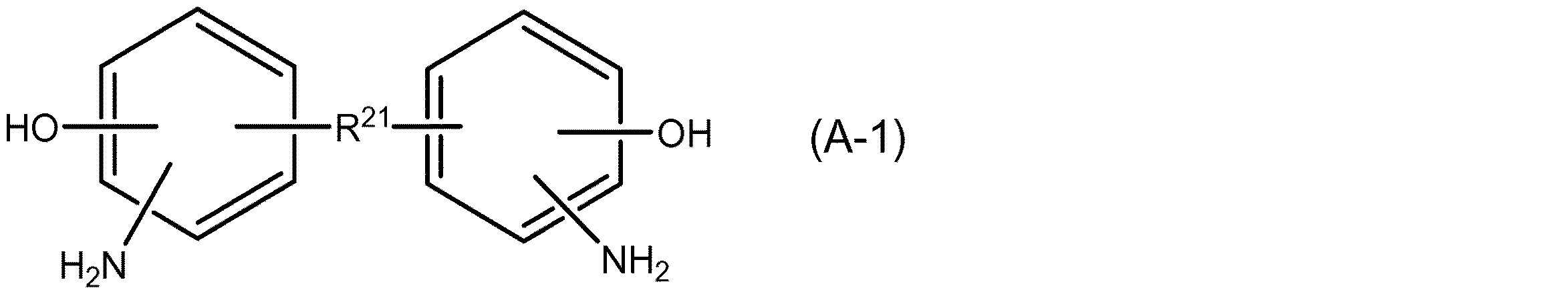
フェノール性水酸基含有ポリイミド樹脂を得るために、下記一般式(A−1)で示されるジアミンを使用することができる。 In order to obtain a phenolic hydroxyl group-containing polyimide resin, a diamine represented by the following general formula (A-1) can be used.
式(A−1)中、R21は、単結合、又は、2価の有機基を示す。
In formula (A-1), R 21 represents a single bond or a divalent organic group.
上記2価の有機基としては、例えば、炭素数1〜30の2価の炭化水素基、又は、ハロゲン原子によって水素の一部若しくは全部が置換されている炭素数1〜30の2価の炭化水素基、−(C=O)−、―SO2−、−O−、−S−、―NH−(C=O)−、―(C=O)−O−、―(Ph)n―、―(Ph―OH)n―などが挙げられる。ここでPhはベンゼン環を示し、nは1〜20の整数を示す。 Examples of the divalent organic group include, for example, a divalent hydrocarbon group having 1 to 30 carbon atoms, or a divalent carbon atom having 1 to 30 carbon atoms in which part or all of hydrogen has been substituted with a halogen atom. Hydrogen group, — (C═O) —, —SO 2 —, —O—, —S—, —NH— (C═O) —, — (C═O) —O—, — (Ph) n — , — (Ph—OH) n — and the like. Here, Ph represents a benzene ring, and n represents an integer of 1 to 20.
上記R21は、ポリイミド樹脂の溶解性の観点から、−C(CF3)2−、−C(CH3)2−が好ましく用いることができる。本実施形態においては、上記フェノール性水酸基を有するジアミンが、下記式(22)で表される、フルオロアルキル基を有するジフェノールジアミンを含むことが好ましい。ポリイミド鎖にフルオロアルキル基が導入されることによって、ポリイミド樹脂の溶剤及び他成分に対する溶解性が向上する。 From the viewpoint of solubility of the polyimide resin, R 21 can be preferably —C (CF 3 ) 2 — or —C (CH 3 ) 2 —. In the present embodiment, the diamine having a phenolic hydroxyl group preferably includes a diphenol diamine having a fluoroalkyl group represented by the following formula (22). By introducing a fluoroalkyl group into the polyimide chain, the solubility of the polyimide resin in the solvent and other components is improved.
上記ポリイミド樹脂の合成時に、単官能酸無水物及び/又は単官能アミンを縮合反応液に投入することにより、ポリマー末端に酸無水物又はジアミン以外の官能基を導入することができる。また、これにより、保存安定性及び熱圧着性を向上させることができる。酸無水物又はジアミン以外の官能基としては、特に限定はしないが、高温接着性を向上させる点で、カルボキシル基やフェノール性水酸基が好ましい。また、良好なフィルム形成性と基材(1)のはく離性を両立できる点で、シロキサン骨格等を有する化合物も好ましく用いられる。 At the time of synthesizing the polyimide resin, a functional group other than the acid anhydride or diamine can be introduced into the polymer terminal by introducing a monofunctional acid anhydride and / or a monofunctional amine into the condensation reaction solution. Thereby, storage stability and thermocompression bonding can be improved. Although it does not specifically limit as functional groups other than an acid anhydride or diamine, A carboxyl group and a phenolic hydroxyl group are preferable at the point which improves high temperature adhesiveness. In addition, a compound having a siloxane skeleton or the like is also preferably used from the viewpoint that both good film formability and peelability of the substrate (1) can be achieved.
(A)熱可塑性樹脂の含有量は、樹脂組成物の固形分全量を基準として5〜90質量%であることが好ましく、20〜80質量%であることがより好ましい。この含有量が5質量%未満であるとフィルム形成性が十分でなくなる傾向があり、90質量%を超えると接着性が十分でなくなる傾向がある。 (A) The content of the thermoplastic resin is preferably 5 to 90 mass%, more preferably 20 to 80 mass%, based on the total solid content of the resin composition. When this content is less than 5% by mass, the film formability tends to be insufficient, and when it exceeds 90% by mass, the adhesion tends to be insufficient.
本実施形態の接着剤層(2)は(B)熱硬化性樹脂を含有する。熱硬化性樹脂としては、分子内に少なくとも2個以上のエポキシ基を含むものが好ましく、熱圧着性や硬化性、硬化物特性の点から、フェノールのグリシジルエーテル型のエポキシ樹脂がより好ましい。このような樹脂としては、例えば、ビスフェノールA型(又はAD型、S型、F型)のグリシジルエーテル、水添加ビスフェノールA型のグリシジルエーテル、エチレンオキシド付加体ビスフェノールA型のグリシジルエーテル、プロピレンオキシド付加体ビスフェノールA型のグリシジルエーテル、フェノールノボラック樹脂のグリシジルエーテル、クレゾールノボラック樹脂のグリシジルエーテル、ビスフェノールAノボラック樹脂のグリシジルエーテル、ナフタレン樹脂のグリシジルエーテル、3官能型(又は4官能型)のグリシジルエーテル、ジシクロペンタジエンフェノール樹脂のグリシジルエーテル、ダイマー酸のグリシジルエステル、3官能型(又は4官能型)のグリシジルアミン、ナフタレン樹脂のグリシジルアミン等が挙げられる。これらは単独で又は2種類以上を組み合わせて使用することができる。 The adhesive layer (2) of the present embodiment contains (B) a thermosetting resin. As the thermosetting resin, those containing at least two epoxy groups in the molecule are preferable, and phenol glycidyl ether type epoxy resins are more preferable from the viewpoint of thermocompression bonding, curability, and cured product characteristics. Examples of such resins include bisphenol A type (or AD type, S type, and F type) glycidyl ether, water-added bisphenol A type glycidyl ether, ethylene oxide adduct bisphenol A type glycidyl ether, and propylene oxide adduct. Bisphenol A type glycidyl ether, phenol novolac resin glycidyl ether, cresol novolac resin glycidyl ether, bisphenol A novolac resin glycidyl ether, naphthalene resin glycidyl ether, trifunctional (or tetrafunctional) glycidyl ether, dicyclo Examples include glycidyl ether of pentadienephenol resin, glycidyl ester of dimer acid, trifunctional (or tetrafunctional) glycidylamine, glycidylamine of naphthalene resin, etc. It is. These can be used alone or in combination of two or more.
また、エポキシ樹脂としては、不純物イオンである、アルカリ金属イオン、アルカリ土類金属イオン、ハロゲンイオン、特に塩素イオンや加水分解性塩素等を300ppm以下に低減した高純度品を用いることが、エレクトロマイグレーション防止や金属導体回路の腐食防止の観点から好ましい。 As the epoxy resin, it is possible to use a high-purity product in which impurity ions such as alkali metal ions, alkaline earth metal ions, halogen ions, particularly chlorine ions and hydrolyzable chlorine are reduced to 300 ppm or less. From the viewpoint of prevention and corrosion prevention of metal conductor circuits.
エポキシ樹脂の含有量は、(A)熱可塑性樹脂100質量部に対して30〜300質量部であることが好ましく、50〜200質量部であることがより好ましい。この含有量が300質量部を超えると、基材(1)に対するフィルム形成性や易はく離性が低下する傾向がある。一方、上記含有量が30質量部未満であると、十分な熱圧着性及び高温接着性が得られなくなる傾向がある。 It is preferable that it is 30-300 mass parts with respect to 100 mass parts of (A) thermoplastic resins, and, as for content of an epoxy resin, it is more preferable that it is 50-200 mass parts. When this content exceeds 300 mass parts, there exists a tendency for the film formability with respect to a base material (1) and easy peelability to fall. On the other hand, when the content is less than 30 parts by mass, there is a tendency that sufficient thermocompression bonding and high-temperature adhesiveness cannot be obtained.
本実施形態の(B)熱硬化性樹脂としては、(B1)固形状エポキシ樹脂と(B2)液状エポキシ樹脂とをともに含むことが好ましい。 The (B) thermosetting resin of this embodiment preferably includes both (B1) a solid epoxy resin and (B2) a liquid epoxy resin.
(B1)固形エポキシ樹脂としては、特に限定はしないが例えば、ビスフェノールA型(又はAD型、S型、F型)のグリシジルエーテル、フェノールノボラック樹脂のグリシジルエーテル、クレゾールノボラック樹脂のグリシジルエーテル、ビスフェノールAノボラック樹脂のグリシジルエーテル、ナフタレン樹脂のグリシジルエーテル、3官能型(又は4官能型)のグリシジルエーテル、ジシクロペンタジエンフェノール樹脂のグリシジルエーテル、等が挙げられ、高温接着性、硬化後の180℃貯蔵弾性率を高度に満足できる点で、下記構造(I)又は(II)で示されるエポキシ樹脂を用いることが最も好ましい。 (B1) The solid epoxy resin is not particularly limited. For example, bisphenol A type (or AD type, S type, F type) glycidyl ether, glycidyl ether of phenol novolac resin, glycidyl ether of cresol novolac resin, bisphenol A Glycidyl ether of novolak resin, glycidyl ether of naphthalene resin, trifunctional (or tetrafunctional) glycidyl ether, glycidyl ether of dicyclopentadienephenol resin, etc., high temperature adhesiveness, 180 ° C storage elasticity after curing It is most preferable to use an epoxy resin represented by the following structure (I) or (II) in that the rate can be highly satisfied.
式(I)中、nは0〜5の整数である。
In formula (I), n is an integer of 0-5.
(B1)液状エポキシ樹脂としては、特に限定はしないが例えば、ビスフェノールA型(又はAD型、S型、F型)のグリシジルエーテル、水添加ビスフェノールA型のグリシジルエーテル、エチレンオキシド付加体ビスフェノールA型のグリシジルエーテル、プロピレンオキシド付加体ビスフェノールA型のグリシジルエーテル、ナフタレン樹脂のグリシジルエーテル、3官能型(又は4官能型)のグリシジルアミン等が挙げられ、シリコンウエハとの密着性、高温接着性、硬化後の180℃貯蔵弾性率を高度に満足できる点で、下記構造(III)で示されるエポキシ樹脂を用いることが最も好ましい。 (B1) Although it does not specifically limit as a liquid epoxy resin, For example, glycidyl ether of bisphenol A type (or AD type, S type, F type), glycidyl ether of water addition bisphenol A type, ethylene oxide adduct bisphenol A type Examples include glycidyl ether, propylene oxide adduct bisphenol A type glycidyl ether, naphthalene resin glycidyl ether, trifunctional (or tetrafunctional) glycidylamine, etc., adhesion to silicon wafer, high temperature adhesion, after curing It is most preferable to use an epoxy resin represented by the following structure (III) from the viewpoint that the 180 ° C. storage elastic modulus can be highly satisfied.
硬化剤としては、例えば、フェノール系化合物、脂肪族アミン、脂環族アミン、芳香族ポリアミン、ポリアミド、脂肪族酸無水物、脂環族酸無水物、芳香族酸無水物、ジシアンジアミド、有機酸ジヒドラジド、三フッ化ホウ素アミン錯体、イミダゾール類、第3級アミン等が挙げられる。これらの中でもフェノール系化合物が好ましく、分子中に少なくとも2個以上のフェノール性水酸基を有するフェノール系化合物がより好ましい。このような化合物としては、例えばフェノールノボラック、クレゾールノボラック、t−ブチルフェノールノボラック、ジシクロペンタジエンクレゾールノボラック、ジシクロペンタジエンフェノールノボラック、キシリレン変性フェノールノボラック、ナフトール系化合物、トリスフェノール系化合物、テトラキスフェノールノボラック、ビスフェノールAノボラック、ポリ−p−ビニルフェノール、フェノールアラルキル樹脂等が挙げられる。これらの中でも、数平均分子量が400〜4000の範囲内のものが好ましい。 Examples of the curing agent include phenolic compounds, aliphatic amines, alicyclic amines, aromatic polyamines, polyamides, aliphatic acid anhydrides, alicyclic acid anhydrides, aromatic acid anhydrides, dicyandiamide, and organic acid dihydrazides. , Boron trifluoride amine complexes, imidazoles, tertiary amines and the like. Among these, phenol compounds are preferable, and phenol compounds having at least two phenolic hydroxyl groups in the molecule are more preferable. Examples of such compounds include phenol novolak, cresol novolak, t-butylphenol novolak, dicyclopentadiene cresol novolak, dicyclopentadiene phenol novolak, xylylene-modified phenol novolak, naphthol compound, trisphenol compound, tetrakisphenol novolak, bisphenol. A novolak, poly-p-vinylphenol, phenol aralkyl resin and the like. Among these, those having a number average molecular weight in the range of 400 to 4000 are preferable.
本実施形態の接着剤層(2)は、(C)硬化促進剤を含有することが好ましい。(C)硬化促進剤としては、加熱によってエポキシの硬化/重合を促進する硬化促進剤を含有させるものであり、例えば、イミダゾール類、ジシアンジアミド誘導体、ジカルボン酸ジヒドラジド、トリフェニルホスフィン、テトラフェニルホスホニウムテトラフェニルボレート、2−エチル−4−メチルイミダゾール−テトラフェニルボレート、1,8−ジアザビシクロ[5.4.0]ウンデセン−7−テトラフェニルボレート等が挙げられる。組成物における硬化促進剤の含有量は、エポキシ樹脂100質量部に対して0.01〜50質量部が好ましい。 The adhesive layer (2) of the present embodiment preferably contains (C) a curing accelerator. (C) The curing accelerator contains a curing accelerator that accelerates the curing / polymerization of epoxy by heating. Examples thereof include imidazoles, dicyandiamide derivatives, dicarboxylic acid dihydrazide, triphenylphosphine, and tetraphenylphosphonium tetraphenyl. Examples thereof include borate, 2-ethyl-4-methylimidazole-tetraphenylborate, 1,8-diazabicyclo [5.4.0] undecene-7-tetraphenylborate. As for content of the hardening accelerator in a composition, 0.01-50 mass parts is preferable with respect to 100 mass parts of epoxy resins.
(C)硬化促進剤としては、フィルム塗工時の反応の抑制と保存安定性の観点から、融点が30℃以上のイミダゾール類であることが好ましく、融点が100℃以上であることが最も好ましい。このようなイミダゾール類としては、特に限定はしないが、1−シアノエチルー2−フェニルイミダゾール、1−シアノエチルー2−フェニルイミダゾリウムトリメリテイト、2,4−ジアミノー6−〔2´−メチルイミダゾリルー(1´)〕−エチルーs―トリアジン、2,4−ジアミノー6−〔2´−メチルイミダゾリルー(1´)〕−エチルーs―トリアジンイソシアヌル酸付加物、2−フェニルー4,5−ジヒドロキシメチルイミダゾール、2−フェニルー4−メチルー5−ヒドロキシメチルイミダゾールなどが挙げられる。 (C) The curing accelerator is preferably an imidazole having a melting point of 30 ° C. or higher, and most preferably 100 ° C. or higher, from the viewpoint of suppressing reaction during film coating and storage stability. . Examples of such imidazoles include, but are not limited to, 1-cyanoethyl-2-phenylimidazole, 1-cyanoethyl-2-phenylimidazolium trimellitate, 2,4-diamino-6- [2′-methylimidazolyl (1 ')]-Ethyl-s-triazine, 2,4-diamino-6- [2'-methylimidazolyl (1')]-ethyl-s-triazine isocyanuric acid adduct, 2-phenyl-4,5-dihydroxymethylimidazole, 2 -Phenyl-4-methyl-5-hydroxymethylimidazole and the like.
上記(C)硬化促進剤は薄膜フィルム形成時の凹凸を抑制するため、5μm以下に粉砕したものを用いることが好ましい。 The (C) curing accelerator is preferably used after being pulverized to 5 μm or less in order to suppress unevenness during the formation of the thin film.
本実施形態の接着剤層(2)は放射線重合性化合物を添加することもできる。放射線重合性化合物としては、エチレン性不飽和基を有する化合物が挙げられ、エチレン性不飽和基としては、ビニル基、アリル基、プロパギル基、ブテニル基、エチニル基、フェニルエチニル基、マレイミド基、ナジイミド基、(メタ)アクリル基などが挙げられ、反応性の観点から、(メタ)アクリル基が好ましい。中でも、ウレタンアクリレート及びメタクリレート、イソシアヌル酸ジ/トリアクリレート及びメタクリレートや2−(1,2−シクロヘキサカルボキシイミド)エチルアクリレートなどのイミド基含有単官能(メタ)アクリレートは硬化後の密着性や高接着性を十分に付与できる点で好ましい。 A radiation polymerizable compound can also be added to the adhesive layer (2) of this embodiment. Examples of the radiation polymerizable compound include compounds having an ethylenically unsaturated group. Examples of the ethylenically unsaturated group include a vinyl group, an allyl group, a propargyl group, a butenyl group, an ethynyl group, a phenylethynyl group, a maleimide group, and a nadiimide. Group, a (meth) acryl group, and the like, and a (meth) acryl group is preferable from the viewpoint of reactivity. Among them, urethane acrylates and methacrylates, isocyanuric acid di / triacrylates and methacrylates, and imide group-containing monofunctional (meth) acrylates such as 2- (1,2-cyclohexacarboxyimide) ethyl acrylate are adhesive and highly adhesive after curing. It is preferable at the point which can fully provide property.
本実施形態の接着剤層(2)はピックアップ性を向上させるために光開始剤を添加することもできる。光開始剤としては、感度向上の点から、波長365nmの光に対する分子吸光係数が100ml/g・cm以上であるものが好ましく、200ml/g・cm以上であるものがより好ましく、400ml/g・cm以上であるものがさらにより好ましく、1000ml/g・cm以上であるものが最も好ましい。なお、分子吸光係数は、サンプルの0.001質量%アセトニトリル溶液を調製し、この溶液について分光光度計(日立ハイテクノロジーズ社製、「U−3310」(商品名))を用いて吸光度を測定することにより求められる。 In the adhesive layer (2) of the present embodiment, a photoinitiator can be added in order to improve pickup properties. As the photoinitiator, those having a molecular extinction coefficient with respect to light having a wavelength of 365 nm are preferably 100 ml / g · cm or more, more preferably 200 ml / g · cm or more, more preferably 400 ml / g · cm from the viewpoint of improving sensitivity. What is more than cm is even more preferable, and what is more than 1000 ml / g · cm is most preferable. As for the molecular extinction coefficient, a 0.001% by mass acetonitrile solution of the sample is prepared, and the absorbance of this solution is measured using a spectrophotometer (manufactured by Hitachi High-Technologies Corporation, “U-3310” (trade name)). Is required.
このような光開始剤としては、例えば、1−ヒドロキシーシクロヘキシルーフェニルーケトン、2−ヒドロキシー2−メチルー1−フェニループロパンー1−オン、1−[4−(2−ヒドロキシエトキシ)−フェニル]−2−ヒドロキシー2−メチルー1−プロパンー1−オン、2−ヒドロキシー1−{4−[4−(2−ヒドロキシー2−メチループロピオニル)−ベンジル]−フェニル}−2−メチループロパンー1−オン、オキシーフェニルーアセチックアシッド2−[2−オキソー2−フェニルーアセトキシーエトキシ]エチルエステル、フェニルグリオキシリック アシッド メチル エステル、2−ジメチルアミノ−2−(4−メチルーベンジル)−1−(4−モルフォリンー4−イルーフェニル)−ブタンー1−オン、2−エチルヘキシルー4−ジメチルアミノベンゾエート、2−ベンジル−2−ジメチルアミノ−1−(4−モルホリノフェニル)−ブタノン−1、2,2−ジメトキシ−1,2−ジフェニルエタン−1−オン、1−ヒドロキシ−シクロヘキシル−フェニル−ケトン、2−メチル−1−(4−(メチルチオ)フェニル)−2−モルフォリノプロパノン−1、2,4−ジエチルチオキサントン、2−エチルアントラキノン、フェナントレンキノン等の芳香族ケトン、ベンジルジメチルケタール等のベンジル誘導体、2−(o−クロロフェニル)−4,5−ジフェニルイミダゾール二量体、2−(o−クロロフェニル)−4,5−ジ(m−メトキシフェニル)イミダゾール二量体、2−(o−フルオロフェニル)−4,5−フェニルイミダゾール二量体、2−(o−メトキシフェニル)−4,5−ジフェニルイミダゾール二量体、2−(p−メトキシフェニル)−4,5−ジフェニルイミダゾール二量体、2,4−ジ(p−メトキシフェニル)−5−フェニルイミダゾール二量体、2−(2,4−ジメトキシフェニル)−4,5−ジフェニルイミダゾール二量体等の2,4,5−トリアリールイミダゾール二量体、9−フェニルアクリジン、1,7−ビス(9,9’−アクリジニル)ヘプタン等のアクリジン誘導体、ビス(2,6−ジメトキシベンゾイル)−2,4,4−トリメチル−ペンチルフォスフィンオキサイド、ビス(2,4,6,−トリメチルベンゾイル)−フェニルフォスフィンオキサイド等のビスアシルフォスフィンオキサイドやマレイミドを有する化合物などが挙げられる。これらは単独で又は2種類以上を組み合わせて使用することができる。 Examples of such a photoinitiator include 1-hydroxy-cyclohexyl phenyl ketone, 2-hydroxy-2-methyl-1-phenyl-propan-1-one, and 1- [4- (2-hydroxyethoxy) -phenyl. ] -2-Hydroxy-2-methyl-1-propan-1-one, 2-hydroxy-1- {4- [4- (2-hydroxy-2-methyl-propionyl) -benzyl] -phenyl} -2-methyl-propane-1 -One, oxy-phenyl-acetic acid 2- [2-oxo-2-phenyl-acetoxy-ethoxy] ethyl ester, phenylglyoxylic acid methyl ester, 2-dimethylamino-2- (4-methyl-benzyl) -1 -(4-morpholin-4-yl-phenyl) -butan-1-one, 2-ethylhexyl -Dimethylaminobenzoate, 2-benzyl-2-dimethylamino-1- (4-morpholinophenyl) -butanone-1,2,2-dimethoxy-1,2-diphenylethan-1-one, 1-hydroxy-cyclohexyl- Aromatic ketones such as phenyl-ketone, 2-methyl-1- (4- (methylthio) phenyl) -2-morpholinopropanone-1,2,4-diethylthioxanthone, 2-ethylanthraquinone, phenanthrenequinone, benzyldimethyl ketal Benzyl derivatives such as 2- (o-chlorophenyl) -4,5-diphenylimidazole dimer, 2- (o-chlorophenyl) -4,5-di (m-methoxyphenyl) imidazole dimer, 2- ( o-fluorophenyl) -4,5-phenylimidazole dimer, 2- (o-meth) Cyphenyl) -4,5-diphenylimidazole dimer, 2- (p-methoxyphenyl) -4,5-diphenylimidazole dimer, 2,4-di (p-methoxyphenyl) -5-phenylimidazole dimer , 2,4,5-triarylimidazole dimer such as 2- (2,4-dimethoxyphenyl) -4,5-diphenylimidazole dimer, 9-phenylacridine, 1,7-bis (9, Acridine derivatives such as 9'-acridinyl) heptane, bis (2,6-dimethoxybenzoyl) -2,4,4-trimethyl-pentylphosphine oxide, bis (2,4,6, -trimethylbenzoyl) -phenylphosphine Examples thereof include bisacylphosphine oxides such as oxides and compounds having maleimide. These can be used alone or in combination of two or more.
さらに、本実施形態においては、フィラーを使用することもできる。前記フィラーとしては、例えば、銀粉、金粉、銅粉、ニッケル粉等の金属フィラー、アルミナ、水酸化アルミニウム、水酸化マグネシウム、炭酸カルシウム、炭酸マグネシウム、ケイ酸カルシウム、ケイ酸マグネシウム、酸化カルシウム、酸化マグネシウム、酸化アルミニウム、窒化アルミニウム、結晶性シリカ、非晶性シリカ、窒化ホウ素、チタニア、ガラス、酸化鉄、セラミック等の無機フィラー、カーボン、ゴム系フィラー等の有機フィラー等が挙げられ、種類・形状等にかかわらず特に制限なく使用することができる。 Furthermore, in this embodiment, a filler can also be used. Examples of the filler include metal fillers such as silver powder, gold powder, copper powder, and nickel powder, alumina, aluminum hydroxide, magnesium hydroxide, calcium carbonate, magnesium carbonate, calcium silicate, magnesium silicate, calcium oxide, and magnesium oxide. Inorganic fillers such as aluminum oxide, aluminum nitride, crystalline silica, amorphous silica, boron nitride, titania, glass, iron oxide, and ceramics, and organic fillers such as carbon and rubber fillers. It can be used without any particular limitation.
上記フィラーは所望する機能に応じて使い分けることができる。例えば、金属フィラーは、接着剤組成物に導電性、熱伝導性、チキソ性等を付与する目的で添加され、非金属無機フィラーは、接着剤層に熱伝導性、低熱膨張性、低吸湿性等を付与する目的で添加され、有機フィラーは接着剤層に靭性等を付与する目的で添加される。これら金属フィラー、無機フィラー又は有機フィラーは、単独で又は二種類以上を組み合わせて使用することができる。中でも、半導体装置用接着材料に求められる、導電性、熱伝導性、低吸湿特性、絶縁性等を付与できる点で、金属フィラー、無機フィラー、又は絶縁性のフィラーが好ましく、無機フィラー、又は絶縁性フィラーの中では、樹脂ワニスに対する分散性が良好でかつ、熱時の高い接着力を付与できる点で窒化ホウ素がより好ましい。 The filler can be used properly according to the desired function. For example, the metal filler is added for the purpose of imparting conductivity, thermal conductivity, thixotropy, etc. to the adhesive composition, and the nonmetallic inorganic filler is thermally conductive, low thermal expansion, low hygroscopicity to the adhesive layer. The organic filler is added for the purpose of imparting toughness to the adhesive layer. These metal fillers, inorganic fillers or organic fillers can be used alone or in combination of two or more. Among them, a metal filler, an inorganic filler, or an insulating filler is preferable, and an inorganic filler or an insulating filler is preferable in that it can provide conductivity, thermal conductivity, low moisture absorption characteristics, insulating properties, and the like required for an adhesive material for a semiconductor device. Among the fillers, boron nitride is more preferable because it has good dispersibility with respect to the resin varnish and can impart a high adhesive force during heating.
上記フィラーの平均粒子径は10μm以下、最大粒子径は25μm以下であり、平均粒子径が5μm以下、最大粒子径が20μm以下であることが好ましい。平均粒子径が10μmを超え、かつ最大粒子径が25μmを超えると、破壊靭性向上の効果が得られない傾向がある。下限は特に制限はないが、通常、どちらも0.01μmである。 The filler preferably has an average particle size of 10 μm or less, a maximum particle size of 25 μm or less, an average particle size of 5 μm or less, and a maximum particle size of 20 μm or less. When the average particle diameter exceeds 10 μm and the maximum particle diameter exceeds 25 μm, the effect of improving fracture toughness tends to be not obtained. Although there is no restriction | limiting in particular in a lower limit, Usually, both are 0.01 micrometer.
上記フィラーの中でも、溶剤への分散性や他の樹脂成分との相溶性、高温接着性の観点から、シリカフィラーが好適に用いられ、エポキシ系、アクリレート系、フェニル系にシランカップリング剤処理されたシリカフィラーが最も好ましく用いられる。 Among the above fillers, silica filler is preferably used from the viewpoint of dispersibility in solvents, compatibility with other resin components, and high-temperature adhesiveness, and is treated with a silane coupling agent in an epoxy system, an acrylate system, or a phenyl system. Silica filler is most preferably used.
上記フィラーは、平均粒子径10μm以下、最大粒子径は25μm以下の両方を満たすことが好ましい。最大粒子径が25μm以下であるが平均粒子径が10μmを超えるフィラーを使用すると、高い接着強度が得られない傾向がある。また、平均粒子径は10μm以下であるが最大粒子径が25μmを超えるフィラーを使用すると、粒径分布が広くなり接着強度にばらつきが出やすくなる。また、本実施形態において、接着剤組成物を薄膜フィルム状に加工して使用する際、表面が粗くなり接着力が低下する傾向がある。 The filler preferably satisfies both an average particle size of 10 μm or less and a maximum particle size of 25 μm or less. When a filler having a maximum particle size of 25 μm or less but an average particle size exceeding 10 μm is used, there is a tendency that high adhesive strength cannot be obtained. Further, when a filler having an average particle size of 10 μm or less but having a maximum particle size exceeding 25 μm is used, the particle size distribution is widened and the adhesive strength tends to vary. Moreover, in this embodiment, when processing and using an adhesive composition in the shape of a thin film, there exists a tendency for the surface to become rough and for adhesive force to fall.
上記フィラーの平均粒子径及び最大粒子径の測定方法としては、例えば、走査型電子顕微鏡(SEM)を用いて、200個程度のフィラーの粒径を測定する方法等が挙げられる。SEMを用いた測定方法としては、例えば、接着剤層を用いて半導体素子と半導体搭載用支持部材とを接着した後、加熱硬化(好ましくは150〜200℃で1〜10時間)させたサンプルを作製し、このサンプルの中心部分を切断して、その断面をSEMで観察する方法等が挙げられる。このとき、前述のフィラーの存在確率が全フィラーの80%以上であることが好ましい。 Examples of the method for measuring the average particle size and the maximum particle size of the filler include a method of measuring the particle size of about 200 fillers using a scanning electron microscope (SEM). As a measuring method using SEM, for example, a sample obtained by adhering a semiconductor element and a semiconductor mounting support member using an adhesive layer and then heat-curing (preferably at 150 to 200 ° C. for 1 to 10 hours) is used. The method of producing, cutting the center part of this sample, and observing the cross section by SEM etc. is mentioned. At this time, it is preferable that the existence probability of the filler is 80% or more of the total filler.
上記フィラーの使用量は、付与する特性、又は機能に応じて決められるが、樹脂成分とフィラーの合計に対して1〜50体積%、好ましくは2〜40体積%、さらに好ましくは5〜30体積%である。フィラーを増量させることにより、高弾性率化が図れ、ダイシング性(ダイサー刃による切断性)、ワイヤボンディング性(超音波効率)、熱時の接着強度を有効に向上できる。フィラーを必要以上に増量させると、本実施形態の特徴である低温貼付性及び被着体との界面接着性が損なわれ、耐リフロー性を含む信頼性の低下を招くため、フィラーの使用量は上記の範囲内に収めることが好ましい。求められる特性のバランスをとるべく、最適フィラー含量を決定する。フィラーを用いた場合の混合・混練は、通常の攪拌機、らいかい機、三本ロール、ボールミル等の分散機を適宜、組み合わせて行うことができる。 Although the usage-amount of the said filler is decided according to the characteristic or function to provide, it is 1-50 volume% with respect to the sum total of a resin component and a filler, Preferably it is 2-40 volume%, More preferably, it is 5-30 volume. %. By increasing the amount of filler, a high elastic modulus can be achieved, and dicing performance (cutability by a dicer blade), wire bonding performance (ultrasonic efficiency), and adhesive strength during heating can be effectively improved. When the filler is increased more than necessary, the low-temperature sticking property and the interfacial adhesion with the adherend, which are the features of this embodiment, are impaired, and the reliability including reflow resistance is reduced. It is preferable to be within the above range. The optimal filler content is determined to balance the required properties. Mixing and kneading in the case of using a filler can be performed by appropriately combining dispersers such as a normal stirrer, a raking machine, a three-roller, and a ball mill.
本実施形態の接着剤組成物には、異種材料間の界面結合を良くするために、各種カップリング剤を添加することもできる。カップリング剤としては、例えば、シラン系、チタン系、アルミニウム系等が挙げられ、中でも効果が高い点で、シラン系カップリング剤が好ましい。上記カップリング剤の使用量は、その効果や耐熱性及びコストの面から、(A)熱可塑性樹脂100重量部に対して、0.01〜20重量部とするのが好ましい。 Various coupling agents can also be added to the adhesive composition of this embodiment in order to improve the interfacial bonding between different materials. Examples of the coupling agent include silane-based, titanium-based, and aluminum-based, and among them, a silane-based coupling agent is preferable because it is highly effective. The amount of the coupling agent used is preferably 0.01 to 20 parts by weight with respect to 100 parts by weight of the thermoplastic resin (A) from the viewpoints of the effect, heat resistance and cost.
本実施形態の接着剤組成物には、イオン性不純物を吸着して、吸湿時の絶縁信頼性を良くするために、さらにイオン捕捉剤を添加することもできる。このようなイオン捕捉剤としては、特に制限はなく、例えば、トリアジンチオール化合物、ビスフェノール系還元剤等の銅がイオン化して溶け出すのを防止するため銅害防止剤として知られる化合物、ジルコニウム系、アンチモンビスマス系マグネシウムアルミニウム化合物等の無機イオン吸着剤などが挙げられる。上記イオン捕捉剤の使用量は、添加による効果や耐熱性、コスト等の点から、上記ポリマー重量部に対して、0.01〜10重量部が好ましい。 In the adhesive composition of the present embodiment, an ion scavenger can be further added in order to adsorb ionic impurities and improve insulation reliability during moisture absorption. Such an ion scavenger is not particularly limited, for example, triazine thiol compound, a compound known as a copper damage inhibitor to prevent copper from being ionized and dissolved, such as a bisphenol-based reducing agent, zirconium-based, Examples include inorganic ion adsorbents such as antimony bismuth-based magnesium aluminum compounds. The amount of the ion scavenger used is preferably 0.01 to 10 parts by weight with respect to the polymer parts by weight from the viewpoint of the effect of addition, heat resistance, cost, and the like.
本実施形態において、接着剤層には、適宜、軟化剤、老化防止剤、着色剤、難燃剤、テルペン系樹脂等の粘着付与剤、熱可塑系高分子成分を添加しても良い。接着性向上、硬化時の応力緩和性を付与するため用いられる熱可塑系高分子成分としては、ポリビニルブチラール樹脂、ポリビニルホルマール樹脂、ポリエステル樹脂、ポリアミド樹脂、ポリイミド樹脂、キシレン樹脂、フェノキシ樹脂、ポリウレタン樹脂、尿素樹脂、アクリルゴム等が挙げられる。これら高分子成分は、分子量が5,000〜500,000のものが好ましい。 In the present embodiment, a softening agent, an anti-aging agent, a colorant, a flame retardant, a tackifier such as a terpene resin, and a thermoplastic polymer component may be appropriately added to the adhesive layer. Thermoplastic polymer components used to improve adhesion and provide stress relaxation during curing include polyvinyl butyral resin, polyvinyl formal resin, polyester resin, polyamide resin, polyimide resin, xylene resin, phenoxy resin, polyurethane resin , Urea resin, acrylic rubber and the like. These polymer components preferably have a molecular weight of 5,000 to 500,000.
本実施形態において基材に積層された接着剤層を他の基材(3)に転写して使用することもできる。このとき使用される基材(3)は25℃での貯蔵弾性率が50〜1000MPaである基材であることが好ましく、基材(3)上に粘着剤層が形成されていても良い。 In this embodiment, the adhesive layer laminated on the substrate can be transferred to another substrate (3) for use. The substrate (3) used at this time is preferably a substrate having a storage elastic modulus at 25 ° C. of 50 to 1000 MPa, and an adhesive layer may be formed on the substrate (3).
基材(3)と接着剤層とのピールはく離強度は20〜300mN/cmであることが好ましく、30〜200mN/cmであることがより好ましい。 The peel strength between the substrate (3) and the adhesive layer is preferably 20 to 300 mN / cm, and more preferably 30 to 200 mN / cm.
基材(3)上に粘着剤層を有しない場合、基材(3)の接着剤層と接する面の表面自由エネルギーは25〜45mN/mであることが好ましく、30〜45mN/mであることが最も好ましい。上記範囲の表面エネルギーを有する基材(3)としては、ポリ塩化ビニル、ポリウレタン、エチレン−酢酸ビニル共重合体などの極性基材、ポリエチレンやポリプロピレンなどの低極性基材にウレタン系、アクリル系、ブタジエン系、ニトリル系などのゴム成分を配合したもの、ポリエチレンやポリプロピレンなどの低極性基材をコロナ処理したものが挙げられる。上記表面自由エネルギーが25mN/mを下回ると接着剤層との密着性が低下し、転写不良により製造歩留まりが低下したり、ダイシング時に半導体チップが飛散したりする傾向がある。また、45mN/mを上回ると接着剤層との密着性が上昇してピックアップ性が損なわれる傾向がある。また、保存安定性やピックアップ性の観点から、接着剤層と接する面にはコロナ処理を行わないことが好ましい。 When the adhesive layer is not provided on the substrate (3), the surface free energy of the surface in contact with the adhesive layer of the substrate (3) is preferably 25 to 45 mN / m, and preferably 30 to 45 mN / m. Most preferred. As the base material (3) having the surface energy in the above range, polar base materials such as polyvinyl chloride, polyurethane, and ethylene-vinyl acetate copolymer, low polar base materials such as polyethylene and polypropylene, urethane type, acrylic type, Examples include those obtained by blending rubber components such as butadiene and nitriles, and those obtained by corona-treating a low-polarity base material such as polyethylene or polypropylene. When the surface free energy is less than 25 mN / m, the adhesiveness with the adhesive layer is lowered, and there is a tendency that the manufacturing yield is lowered due to transfer failure, and the semiconductor chip is scattered during dicing. Moreover, when it exceeds 45 mN / m, there exists a tendency for adhesiveness with an adhesive bond layer to rise and for pick-up property to be impaired. Further, from the viewpoint of storage stability and pick-up properties, it is preferable not to perform corona treatment on the surface in contact with the adhesive layer.
上記基材(3)としては、エステル骨格を有するポリマーを少なくとも有することが好ましい。エステル骨格を有するポリマーとしては、ポリエチレンテレフタレート、ポリブチレンテレフタレートの他に、テレフタル酸の代わりに脂肪族カルボン酸を併用したポリエステルや、長鎖脂肪族ジオールを併用したポリエステルなどの主鎖にエステル骨格を有するポリエステルが挙げられる。また、エチレン−酢酸ビニル共重合体やポリメタクリル酸メチルなどの側鎖にエステル基を有するポリマーが挙げられる。 The substrate (3) preferably has at least a polymer having an ester skeleton. In addition to polyethylene terephthalate and polybutylene terephthalate, the polymer having an ester skeleton has an ester skeleton in the main chain, such as a polyester using an aliphatic carboxylic acid instead of terephthalic acid, or a polyester using a long-chain aliphatic diol. The polyester which has is mentioned. Moreover, the polymer which has an ester group in side chains, such as an ethylene-vinyl acetate copolymer and polymethyl methacrylate, is mentioned.
前記エステル基を有するポリマーは、ポリエチレンやポリプロピレンなどの低表面エネルギー基材に含有させることもでき、所望の表面エネルギーとエキスパンド性を両立することができる。 The polymer having an ester group can be contained in a low surface energy base material such as polyethylene or polypropylene, and can achieve both desired surface energy and expandability.
前記基材(3)は、下記一般式(23)で表されるポリブチレンテレフタレート骨格を有するポリマーを少なくとも含有することが好ましい。前記ポリマーを適用することで接着剤との密着に必要な高い表面エネルギーとピックアップ時に必要なエキスパンド性を高度に両立することができる。 The substrate (3) preferably contains at least a polymer having a polybutylene terephthalate skeleton represented by the following general formula (23). By applying the polymer, it is possible to achieve both high surface energy necessary for adhesion with the adhesive and expandability necessary for pickup.
また基材(3)は、エチレン酢酸ビニル共重合体を少なくとも含有することが好ましい。 Moreover, it is preferable that a base material (3) contains an ethylene vinyl acetate copolymer at least.
本実施形態の接着フィルムは、IC、LSI等の半導体素子と、42アロイリードフレーム、銅リードフレーム等のリードフレーム;ポリイミド樹脂、エポキシ樹脂等のプラスチックフィルム;ガラス不織布等基材にポリイミド樹脂、エポキシ樹脂等のプラスチックを含浸、硬化させたもの;アルミナ等のセラミックス等の半導体搭載用支持部材等の被着体とを貼り合せるためのダイボンディング用接着材料として用いることができる。中でも、表面に有機レジスト層を具備してなる有機基板、表面に配線有する有機基板等の表面に凹凸を有する有機基板と半導体素子とを接着するためのダイボンディング用接着材料として好適に用いられる。 The adhesive film of this embodiment includes semiconductor elements such as IC and LSI, lead frames such as 42 alloy lead frames and copper lead frames; plastic films such as polyimide resins and epoxy resins; What is impregnated and cured with plastic such as resin; can be used as an adhesive material for die bonding for bonding an adherend such as a semiconductor mounting support member such as ceramics such as alumina. Among them, it is suitably used as an adhesive material for die bonding for bonding an organic substrate having an uneven surface on a surface such as an organic substrate having an organic resist layer on the surface and an organic substrate having wiring on the surface, and a semiconductor element.
また、複数の半導体素子を積み重ねた構造のStacked−PKGにおいて、半導体素子と半導体素子とを接着するための接着材料としても好適に用いられる。 Further, in the Stacked-PKG having a structure in which a plurality of semiconductor elements are stacked, it is also suitably used as an adhesive material for bonding the semiconductor elements to the semiconductor elements.
(半導体装置)
本実施形態の半導体用接着フィルムを備える半導体装置について説明する。尚、近年は様々な構造の半導体装置が提案されており、本実施形態の半導体用接着フィルムの用途は、以下に説明する構造の半導体装置に限定されるものではない。
(Semiconductor device)
A semiconductor device provided with the adhesive film for semiconductors of this embodiment is demonstrated. In recent years, semiconductor devices having various structures have been proposed, and the application of the adhesive film for a semiconductor according to the present embodiment is not limited to the semiconductor device having the structure described below.
半導体装置の一形態では、半導体素子が本実施形態の半導体用接着フィルムを介して半導体搭載用支持部材に接着され、半導体素子の接続端子はワイヤを介して外部接続端子と電気的に接続され、封止材によって封止されている。 In one form of the semiconductor device, the semiconductor element is bonded to the semiconductor mounting support member through the semiconductor adhesive film of the present embodiment, and the connection terminal of the semiconductor element is electrically connected to the external connection terminal through the wire, It is sealed with a sealing material.
半導体装置の他の形態では、一段目の半導体素子が本実施形態の半導体用接着フィルムを介して半導体搭載用支持部材に接着され、一段目の半導体素子の上に更に本実施形態の半導体用接着フィルムを介して二段目の半導体素子が接着されている。一段目の半導体素子及び二段目の半導体素子の接続端子は、ワイヤを介して外部接続端子と電気的に接続され、封止材によって封止されている。このように、本実施形態の半導体用接着フィルムは、半導体素子を複数重ねる構造の半導体装置にも好適に使用できる。 In another form of the semiconductor device, the first stage semiconductor element is bonded to the semiconductor mounting support member via the semiconductor adhesive film of the present embodiment, and the semiconductor bond of the present embodiment is further formed on the first stage semiconductor element. A second-stage semiconductor element is bonded via a film. The connection terminals of the first-stage semiconductor element and the second-stage semiconductor element are electrically connected to external connection terminals via wires and sealed with a sealing material. Thus, the adhesive film for a semiconductor according to the present embodiment can be suitably used for a semiconductor device having a structure in which a plurality of semiconductor elements are stacked.
尚、前記構造を備える半導体装置(半導体パッケージ)は、半導体素子と半導体搭載用支持部材との間に本実施形態の半導体用接着フィルムを挾み、加熱圧着して両者を接着させ、その後ワイヤボンディング工程、必要に応じて封止材による封止工程等の工程を経ることにより得られる。 In the semiconductor device (semiconductor package) having the above structure, the semiconductor adhesive film of this embodiment is sandwiched between the semiconductor element and the semiconductor mounting support member, and the two are bonded by thermocompression bonding, and then wire bonding is performed. It is obtained by passing through processes, such as a sealing process with a sealing material, as necessary.
<(A)熱可塑性樹脂>
(PI−1)
撹拌機、温度計及び窒素置換装置(窒素流入管)を備えた500mLフラスコ内に、ジアミンである2−ビス[4−(4−アミノフェノキシ)フェニル]プロパン(商品名「BAPP」、分子量410、和歌山精化工業社製)を12.3g(0.03mol)、ポリオキシプロピレンジアミン(商品名「D−400」(分子量:433)、BASF社製)を26.0g(0.06mol)、及びアミノ変性シリコーンオイル(商品名「KF―8010」、分子量860、信越シリコーン社製)を8.6g(0.01mol)と、溶媒であるNMP(N−メチル−2−ピロリドン)250gを仕込み、撹拌してジアミンを溶媒に溶解させた。
<(A) Thermoplastic resin>
(PI-1)
In a 500 mL flask equipped with a stirrer, a thermometer and a nitrogen displacement device (nitrogen inflow pipe), 2-bis [4- (4-aminophenoxy) phenyl] propane (trade name “BAPP”, molecular weight 410, 12.3 g (0.03 mol) of Wakayama Seika Kogyo Co., Ltd., 26.0 g (0.06 mol) of polyoxypropylenediamine (trade name “D-400” (molecular weight: 433), manufactured by BASF), and 8.6 g (0.01 mol) of amino-modified silicone oil (trade name “KF-8010”, molecular weight 860, manufactured by Shin-Etsu Silicone) and 250 g of NMP (N-methyl-2-pyrrolidone) as a solvent were added and stirred. The diamine was dissolved in the solvent.
上記フラスコに、デカメチレンビストリメリテート二無水物(以下「DBTA」、分子量522〕53.2g(0.102mol)を、フラスコ内の溶液に添加した。添加終了後、窒素ガスを吹き込みながら室温で1時間撹拌した。その後、フラスコに水分受容器付きの還流冷却器を取り付け、溶液を180℃に昇温させて5時間保温してポリイミド樹脂(PI−1)を得た。(PI−1)のGPC測定(Gel permeation Chromatography)を行ったところ、ポリスチレン換算でMw=70000であった。また、(PI−1)のTgは45℃であった。なお、(PI−1)は、上記一般式(A)で表わされる樹脂に該当する。 To the flask, 53.2 g (0.102 mol) of decamethylene bistrimellitate dianhydride (hereinafter “DBTA”, molecular weight 522) was added to the solution in the flask. After stirring for 1 hour, a reflux condenser with a moisture receiver was attached to the flask, and the solution was heated to 180 ° C. and kept for 5 hours to obtain a polyimide resin (PI-1). As a result of GPC measurement (Gel permeation Chromatography), Mw was 70000 in terms of polystyrene, and Tg of (PI-1) was 45 ° C. In addition, (PI-1) This corresponds to the resin represented by the formula (A).
(PI−2)
撹拌機、温度計及び窒素置換装置(窒素流入管)を備えた500mLフラスコ内に、ジアミンである,1,4−ブタンジオール ビス(3−アミノプロピル)エーテル(商品名「B−12」、東京化成製、分子量204.31)8.17g(0.04mol)、ポリオキシプロピレンジアミン(商品名「D−400」(分子量:433)、BASF社製)21.65g(0.05mol)、及びアミノ変性シリコーンオイル(商品名「KF―8010」、分子量860、信越シリコーン社製)8.6g(0.01mol)と、溶媒であるNMP(N−メチル−2−ピロリドン)250gを仕込み、撹拌してジアミンを溶媒に溶解させた。
(PI-2)
In a 500 mL flask equipped with a stirrer, a thermometer, and a nitrogen displacement device (nitrogen inflow pipe), 1,4-butanediol bis (3-aminopropyl) ether (trade name “B-12”, Tokyo), which is a diamine. Kasei, molecular weight 204.31) 8.17 g (0.04 mol), polyoxypropylenediamine (trade name “D-400” (molecular weight: 433), manufactured by BASF) 21.65 g (0.05 mol), and amino 8.6 g (0.01 mol) of a modified silicone oil (trade name “KF-8010”, molecular weight 860, manufactured by Shin-Etsu Silicone) and 250 g of NMP (N-methyl-2-pyrrolidone) as a solvent are charged and stirred. The diamine was dissolved in the solvent.
上記フラスコに、4,4´−オキシジフタル酸二無水物(以下「ODPA」、分子量310〕31.6g(0.102mol)を、フラスコ内の溶液に添加した。添加終了後、窒素ガスを吹き込みながら室温で1時間撹拌した。その後、フラスコに水分受容器付きの還流冷却器を取り付け、溶液を180℃に昇温させて5時間保温してポリイミド樹脂(PI−2)を得た。(PI−2)のGPC測定を行ったところ、ポリスチレン換算でMw=50000であった。また、(PI−2)のTgは50℃であった。なお、(PI−2)は、上記一般式(A)で表わされる樹脂に該当する。 To the flask, 31.6 g (0.102 mol) of 4,4′-oxydiphthalic dianhydride (hereinafter “ODPA”, molecular weight 310) was added to the solution in the flask. The mixture was stirred at room temperature for 1 hour, and then a reflux condenser with a moisture receiver was attached to the flask, and the solution was heated to 180 ° C. and kept for 5 hours to obtain a polyimide resin (PI-2). When GPC measurement of 2) was performed, it was Mw = 50000 in terms of polystyrene, and Tg of (PI-2) was 50 ° C. In addition, (PI-2) is represented by the above general formula (A). ).
(PI−3)
撹拌機、温度計及び窒素置換装置(窒素流入管)を備えた500mLフラスコ内に、ジアミンである,BAPPを12.3g(0.03mol)、D−400を26.0g(0.06mol)と、1,1,3,3−テトラメチル−1,3−ビス(3−アミノプロピル)ジシロキサン(商品名「BY16−871EG」、東レ・ダウコーニング(株)製)2.485g(0.01mol)と、溶媒であるNMP250gを仕込み、撹拌してジアミンを溶媒に溶解させた。
(PI-3)
In a 500 mL flask equipped with a stirrer, a thermometer, and a nitrogen displacement device (nitrogen inlet pipe), 12.3 g (0.03 mol) of BAPP and 26.0 g (0.06 mol) of D-400 are diamines. 1,1,3,3-tetramethyl-1,3-bis (3-aminopropyl) disiloxane (trade name “BY16-871EG”, manufactured by Toray Dow Corning Co., Ltd.) 2.485 g (0.01 mol) ) And 250 g of NMP as a solvent were added and stirred to dissolve the diamine in the solvent.
上記フラスコに、DBTAを53.2g(0.102mol)フラスコ内の溶液に添加した。添加終了後、窒素ガスを吹き込みながら室温で1時間撹拌した。その後、フラスコに水分受容器付きの還流冷却器を取り付け、溶液を180℃に昇温させて5時間保温してポリイミド樹脂(PI−3)を得た。(PI−3)のGPC測定を行ったところ、ポリスチレン換算でMw=70000であった。また、(PI−3)のTgは45℃であった。 To the flask, DBTA was added to the solution in the 53.2 g (0.102 mol) flask. After completion of the addition, the mixture was stirred at room temperature for 1 hour while blowing nitrogen gas. Thereafter, a reflux condenser with a moisture acceptor was attached to the flask, and the solution was heated to 180 ° C. and kept for 5 hours to obtain a polyimide resin (PI-3). When GPC measurement of (PI-3) was performed, it was Mw = 70000 in terms of polystyrene. Moreover, Tg of (PI-3) was 45 ° C.
<基材>
下記の機材を準備した。
基材a:ポリエチレンテレフタレート系(フィルム厚:50μm、離型剤処理あり、表面エネルギー:13mN/m)。
基材b:ポリエチレンテレフタレート系(フィルム厚:50μm、離型剤処理あり、表面エネルギー:26mN/m)。
基材c:ポリプロピレン系(フィルム厚:75μm、離型剤処理なし、表面エネルギー:38mN/m)。
<Base material>
The following equipment was prepared.
Base material a: Polyethylene terephthalate type (film thickness: 50 μm, with release agent treatment, surface energy: 13 mN / m).
Substrate b: Polyethylene terephthalate system (film thickness: 50 μm, with release agent treatment, surface energy: 26 mN / m).
Substrate c: Polypropylene (film thickness: 75 μm, no release agent treatment, surface energy: 38 mN / m).
<接着剤組成物>
上記で得られたポリイミド樹脂(PI−1)〜(PI−3)を用いて、下記表1,2に示す組成比(単位:質量部)にて各成分を配合し、実施例1〜7及び比較例1及び2の接着剤組成物(接着剤層形成用ワニス)を得た。
<Adhesive composition>
Using the polyimide resins (PI-1) to (PI-3) obtained above, the respective components were blended at the composition ratios (unit: parts by mass) shown in Tables 1 and 2 below. Examples 1 to 7 And the adhesive composition (varnish for adhesive layer formation) of Comparative Examples 1 and 2 was obtained.
表1,2において、各記号は下記のものを意味する。
1032H60:ジャパンエポキシレジン社製、トリス(ヒドロキシフェニル)メタン型エポキシ樹脂(5%重量減少温度:350℃、固形エポキシ、軟化点60℃)。なお1032H60は、上記化学式(I)で表わされる。
EXA―4710:DIC社製、ナフタレン型エポキシ樹脂(5%重量減少温度:400℃、固形エポキシ、軟化点95℃)。なおEXA―4710は、上記化学式(II)で表わされる。
HP―7200::DIC社製、ジシクロペンタジエン型エポキシ樹脂(5%重量減少温度:300℃、固形エポキシ、軟化点60℃)。
YDF−8170C:東都化成社製、ビスフェノールF型ビスグリシジルエーテル(5%重量減少温度:270℃、液状エポキシ)。
2PHZ−PW:四国化成社製、2−フェニル−4,5−ジヒドロキシメチルイミダゾール(平均粒子径:約3μm)。
NMP:関東化学社製、N−メチル−2−ピロリドン。
In Tables 1 and 2, each symbol means the following.
1032H60: manufactured by Japan Epoxy Resin Co., Ltd., tris (hydroxyphenyl) methane type epoxy resin (5% weight loss temperature: 350 ° C., solid epoxy, softening point 60 ° C.). 1032H60 is represented by the above chemical formula (I).
EXA-4710: manufactured by DIC, naphthalene type epoxy resin (5% weight loss temperature: 400 ° C., solid epoxy, softening point 95 ° C.). EXA-4710 is represented by the above chemical formula (II).
HP-7200 :: dicyclopentadiene type epoxy resin manufactured by DIC (5% weight loss temperature: 300 ° C., solid epoxy, softening point 60 ° C.).
YDF-8170C: manufactured by Tohto Kasei Co., Ltd., bisphenol F type bisglycidyl ether (5% weight loss temperature: 270 ° C., liquid epoxy).
2PHZ-PW: manufactured by Shikoku Kasei Co., Ltd., 2-phenyl-4,5-dihydroxymethylimidazole (average particle size: about 3 μm).
NMP: N-methyl-2-pyrrolidone manufactured by Kanto Chemical Co., Inc.
<接着フィルム>
以下に示す方法で、表1,2に示す構成を有する各実施例及び比較例の半導体用接着フィルムを作製した。まず、得られた接着剤組成物を、アプリケーター(YBA−5型、ヨシミツ精機社製)を用いて乾燥後に所定の膜厚となるように、それぞれ剥離剤で処理された基材上に塗布し、オーブン中にて80℃で20分間加熱し、続いて120℃で20分間加熱して、基材上に接着剤組成物からなる接着剤層を形成した。このようにして、基材及び基材上に形成された接着剤層を有する各実施例及び比較例の接着フィルムを得た。
<Adhesive film>
By the method shown below, adhesive films for semiconductors of Examples and Comparative Examples having the configurations shown in Tables 1 and 2 were produced. First, the obtained adhesive composition was applied onto a substrate treated with a release agent so that the film thickness would be a predetermined thickness after drying using an applicator (YBA-5 type, manufactured by Yoshimitsu Seiki Co., Ltd.). Then, heating was carried out at 80 ° C. for 20 minutes in an oven, followed by heating at 120 ° C. for 20 minutes to form an adhesive layer made of the adhesive composition on the substrate. Thus, the adhesive film of each Example and comparative example which has a base material and the adhesive bond layer formed on the base material was obtained.
<評価試験>
[フィルム形成性]
前記接着フィルムの作製方法と同様にして、アプリケーター(YBA−5型、ヨシミツ精機社製)を用いて200mm×200mmの大きさの接着フィルムを作製してフィルム形成性を目視評価した。フィルム内にピンホールやはじきが観測されなかったものをA、直径1cm以上のピンホールやはじきが観測されたものをCとした。評価結果を表1,2に示す。
<Evaluation test>
[Film formability]
In the same manner as the method for producing the adhesive film, an adhesive film having a size of 200 mm × 200 mm was produced using an applicator (YBA-5 type, manufactured by Yoshimitsu Seiki Co., Ltd.), and the film formability was visually evaluated. A film in which no pinhole or repellency was observed was A, and a film in which pinholes or repellations with a diameter of 1 cm or more were observed was C. The evaluation results are shown in Tables 1 and 2.
[基材(1)の表面自由エネルギー]
基材の接着剤層が形成される側の表面自由エネルギーを下記の方法で測定した。基材a及びbの場合、基材のはく離剤で処理された面について測定を行った。基材cの場合、はく離剤で処理されていない面について測定を行った。各基材の測定面に対して水、グリセリン及びホルムアミドをプローブ液体としたときの接触角を接触角計(DropMaster 500、協和界面科学社製)を用いて、液適量1μL、測定温度25℃にて測定し、接触角計に搭載の解析ソフト(FAMAS、協和界面科学社製)を用いて酸−塩基法により、基材の表面自由エネルギーを求めた。結果を表1,2に示す。なお、表中の「表面エネルギー」とは、表面自由エネルギーと同義である。
[Surface free energy of substrate (1)]
The surface free energy on the side where the adhesive layer of the substrate was formed was measured by the following method. In the case of the base materials a and b, the surface of the base material treated with a release agent was measured. In the case of the base material c, the measurement was performed on the surface that was not treated with the release agent. Using a contact angle meter (DropMaster 500, manufactured by Kyowa Interface Science Co., Ltd.), the contact angle when water, glycerin and formamide were used as probe liquids on the measurement surface of each substrate was adjusted to an appropriate amount of 1 μL and a measurement temperature of 25 ° C. The surface free energy of the substrate was determined by an acid-base method using analysis software (FAMAS, manufactured by Kyowa Interface Science Co., Ltd.) mounted on the contact angle meter. The results are shown in Tables 1 and 2. The “surface energy” in the table is synonymous with surface free energy.
[接着剤層(2)の表面自由エネルギー]
前記方法で作製した接着フィルムの接着剤層に対して水、グリセリン及びホルムアミドをプローブ液体としたときの接触角を接触角計(DropMaster 500、協和界面科学社製)を用いて、液適量1μL、測定温度25℃にて測定し、接触角計に搭載の解析ソフト(FAMAS、協和界面科学社製)を用いて酸−塩基法により、接着剤層の表面自由エネルギーを求めた。結果を表1,2に示す。
[Surface free energy of adhesive layer (2)]
Using a contact angle meter (DropMaster 500, manufactured by Kyowa Interface Science Co., Ltd.), an appropriate amount of liquid of 1 μL for the contact angle when water, glycerin and formamide are used as probe liquids for the adhesive layer of the adhesive film produced by the above method, Measurement was performed at a measurement temperature of 25 ° C., and the surface free energy of the adhesive layer was determined by an acid-base method using analysis software (FAMAS, manufactured by Kyowa Interface Science Co., Ltd.) installed in the contact angle meter. The results are shown in Tables 1 and 2.
[基材(1)と接着剤層(2)とのピールはく離強度(X)]
前記方法で、幅1cm、長さ4cmの短冊状の接着フィルムを作製した。6インチシリコンウエハ(厚さ400μm)の裏面に対して接着剤層を向けた状態で、接着フィルムを温度50℃でシリコンウエハに対して圧着(線圧4kgf/cm、送り速度0.5m/分)することによりサンプルを作製した。圧着にはロールを用いた。得られたサンプルのシリコンウエハ部分を固定し、基材(1)の端部の一部を接着剤層(2)からはく離させる90度引張はく離試験により測定された値の最大値をピールはく離強度(X)とした。測定装置は株式会社東洋精機製作所社製ストログラフE−S(剥離速度50mm/min、25℃)を使用した。結果を表1,2に示す。なお、表中の「基材(1)/接着層(2)間密着性」は、ピールはく離強度(X)と同義である。
[Peel peel strength (X) between substrate (1) and adhesive layer (2)]
By the above method, a strip-like adhesive film having a width of 1 cm and a length of 4 cm was produced. With the adhesive layer facing the back of a 6-inch silicon wafer (thickness 400 μm), the adhesive film is pressure-bonded to the silicon wafer at a temperature of 50 ° C. (linear pressure 4 kgf / cm, feed rate 0.5 m / min) ) To prepare a sample. A roll was used for pressure bonding. Fix the silicon wafer part of the obtained sample, peel off the maximum value measured by the 90 degree tensile peel test that peels off part of the edge of the substrate (1) from the adhesive layer (2) (X). As a measuring device, Strograph ES (peeling speed 50 mm / min, 25 ° C.) manufactured by Toyo Seiki Seisakusho Co., Ltd. was used. The results are shown in Tables 1 and 2. In the table, “adhesion between substrate (1) / adhesive layer (2)” has the same meaning as peel peel strength (X).
[接着剤層の溶融温度]
10μmの接着剤層を複数積層して50℃でロール加圧(線圧4kgf/cm、送り速度0.5m/分)することにより作製した厚さ100μmのサンプルを5mm幅の短冊状に切断し、レオメトリックス社製粘弾性アナライザー「RSA−2」(商品名)を用いて、昇温速度5℃/min、周波数1Hz、測定温度−50〜100℃の条件で測定を行ったときのtanδピーク温度を接着剤層の溶融温度(ガラス転移温度)とした。結果を表1,2に示す。
[Melting temperature of adhesive layer]
A plurality of 10 μm adhesive layers are stacked and roll-pressed at 50 ° C. (linear pressure 4 kgf / cm, feed rate 0.5 m / min), and a 100 μm thick sample is cut into a 5 mm wide strip. Tan δ peak when measured under the conditions of a heating rate of 5 ° C./min, a frequency of 1 Hz, and a measurement temperature of −50 to 100 ° C. using a rheometrics viscoelasticity analyzer “RSA-2” (trade name) The temperature was defined as the melting temperature (glass transition temperature) of the adhesive layer. The results are shown in Tables 1 and 2.
[接着剤層の120℃での溶融粘度]
10μmの接着剤層を複数積層して50℃でロール加圧(線圧4kgf/cm、送り速度0.5m/分)することにより作製した厚さ100μmのサンプルの120℃での溶融粘度を、粘弾性測定装置ARES(レオメトリックス・サイエンティフィック・エフ・イー(株)製)を用いて測定した。なお、測定プレートは直径20mmの平行プレート、測定条件は昇温5℃/min、測定温度は−50℃〜200℃、周波数は1Hzとする。結果を表1,2に示す。
[Melt viscosity at 120 ° C. of adhesive layer]
The melt viscosity at 120 ° C. of a 100 μm thick sample prepared by laminating a plurality of 10 μm adhesive layers and roll pressing at 50 ° C. (linear pressure 4 kgf / cm, feed rate 0.5 m / min), It measured using the viscoelasticity measuring apparatus ARES (made by Rheometrics Scientific F.E. Co., Ltd.). The measurement plate is a parallel plate having a diameter of 20 mm, the measurement conditions are a temperature increase of 5 ° C./min, the measurement temperature is −50 ° C. to 200 ° C., and the frequency is 1 Hz. The results are shown in Tables 1 and 2.
[接着剤層の熱硬化後の180℃での貯蔵弾性率]
10μmの接着剤層を複数積層して50℃でロール加圧(線圧4kgf/cm、送り速度0.5m/分)することにより厚さ100μmのサンプルをテフロンシート上に作製し、150℃で1時間、次いで180℃で1時間オーブンで熱硬化した。得られたサンプルを5mm幅の短冊状に切断し、レオメトリックス社製粘弾性アナライザー「RSA−2」(商品名)を用いて、昇温速度5℃/min、周波数1Hz、測定温度−50〜200℃の条件で、サンプルの180℃での貯蔵弾性率を測定した。結果を表1,2に示す。
[Storage modulus at 180 ° C. after heat curing of adhesive layer]
A plurality of 10 μm adhesive layers are laminated and roll-pressed at 50 ° C. (linear pressure 4 kgf / cm, feed rate 0.5 m / min) to prepare a 100 μm-thick sample on a Teflon sheet at 150 ° C. Heat cured in an oven for 1 hour and then at 180 ° C. for 1 hour. The obtained sample was cut into a strip having a width of 5 mm, and using a viscoelasticity analyzer “RSA-2” (trade name) manufactured by Rheometrix Co., Ltd., the temperature rising rate was 5 ° C./min, the frequency was 1 Hz, and the measurement temperature was −50 to The storage elastic modulus at 180 ° C. of the sample was measured under the condition of 200 ° C. The results are shown in Tables 1 and 2.
[260℃接着強度]
前記方法で作製した接着フィルムをシリコンウエハ上に50℃でロール加圧して積層した。得られたシリコンウエハ/接着剤層/基材の構造体から基材をはく離除去した後、シリコンウエハ/接着剤層の構造体を3mm×3mmの大きさに個片化して、接着剤層付シリコンチップを得た。個片化した接着剤層付シリコンチップを予めダイシングしたシリコンチップ(10mm×10mm×0.40mm)の鏡面側に積層し、100gfで加圧しながら、120℃で1秒間圧着した。このようにして、シリコンウエハ、接着剤層及びシリコンウエハからなり、これらがこの順に積層する積層体のサンプルを得た。
[260 ° C adhesive strength]
The adhesive film produced by the above method was laminated on a silicon wafer by roll pressing at 50 ° C. After removing the substrate from the obtained silicon wafer / adhesive layer / substrate structure, the silicon wafer / adhesive layer structure was separated into 3 mm × 3 mm pieces and attached with an adhesive layer. A silicon chip was obtained. The separated silicon chip with an adhesive layer was laminated on the mirror surface side of a previously diced silicon chip (10 mm × 10 mm × 0.40 mm) and pressed at 120 ° C. for 1 second while being pressurized with 100 gf. Thus, the sample of the laminated body which consists of a silicon wafer, an adhesive bond layer, and a silicon wafer and these are laminated | stacked in this order was obtained.
得られたサンプルを、オーブン中で150℃、1時間、次いで180℃、1時間の条件で加熱し、さらに、260℃の熱盤上で10秒間加熱した後、せん断接着力試験機「Dage−4000」(商品名)を用いてシリコンウエハ間の接着力(260℃接着強度)を測定した。測定結果を表1,2に示す。 The obtained sample was heated in an oven at 150 ° C. for 1 hour, then at 180 ° C. for 1 hour, and further heated on a hot plate at 260 ° C. for 10 seconds, and then the shear adhesion tester “Dage- 4000 ”(trade name) was used to measure the adhesive strength between silicon wafers (260 ° C. adhesive strength). The measurement results are shown in Tables 1 and 2.
1・・・基材、2・・・接着剤層、100・・・半導体用接着フィルム。
DESCRIPTION OF
Claims (9)
熱可塑性樹脂及び熱硬化性樹脂を含有し、表面自由エネルギーが15〜25mN/mであり、厚さが10μm以下であり、前記基材に積層された接着剤層と、を備え、
前記基材と前記接着剤層とのピール剥離強度が1〜50mN/cmである、
半導体用接着フィルム。 A substrate;
An adhesive layer containing a thermoplastic resin and a thermosetting resin, having a surface free energy of 15 to 25 mN / m, a thickness of 10 μm or less, and laminated on the substrate;
The peel peel strength between the substrate and the adhesive layer is 1 to 50 mN / cm.
Adhesive film for semiconductors.
請求項1に記載の半導体用接着フィルム。 The surface free energy of the surface in contact with the adhesive layer of the substrate is 10 to 30 mN / m.
The adhesive film for a semiconductor according to claim 1.
前記接着剤層の120℃での溶融粘度が20000Pa・s以下である、
請求項1又は2に記載の半導体用接着フィルム。 The glass transition temperature of the thermoplastic resin is 80 ° C. or less,
The melt viscosity at 120 ° C. of the adhesive layer is 20000 Pa · s or less,
The adhesive film for semiconductors according to claim 1 or 2.
前記ポリイミド樹脂が下記一般式(A)で示される構造体を少なくとも含む、
請求項1〜3のいずれかに記載の半導体用接着フィルム。
[式(A)中、Xは4価の有機基であり、nは3〜30の整数である。] The thermoplastic resin includes a polyimide resin;
The polyimide resin contains at least a structure represented by the following general formula (A),
The adhesive film for semiconductors in any one of Claims 1-3.
[In Formula (A), X is a tetravalent organic group, n is an integer of 3-30. ]
請求項1〜4のいずれかに記載の半導体用接着フィルム。 The storage elastic modulus at 180 ° C. after thermosetting of the adhesive layer is 10 MPa or more,
The adhesive film for semiconductors in any one of Claims 1-4.
請求項1〜5のいずれかに記載の半導体用接着フィルム。
[式(I)中、nは0〜5の整数である。] The adhesive layer contains at least a resin represented by the following chemical formula (I) or (II) as the thermosetting resin.
The adhesive film for semiconductors in any one of Claims 1-5.
[In Formula (I), n is an integer of 0-5. ]
前記半導体用接着フィルムの前記接着剤層上に積層されたダイシングシートと、を備える、
接着シート。 An adhesive film for a semiconductor according to any one of claims 1 to 6;
A dicing sheet laminated on the adhesive layer of the adhesive film for a semiconductor,
Adhesive sheet.
前記半導体用接着フィルムを用いて互いに接着された複数の半導体素子、を備える、
半導体装置。
A semiconductor element and a semiconductor mounting support member bonded using the semiconductor adhesive film according to claim 1, and / or
A plurality of semiconductor elements bonded to each other using the adhesive film for a semiconductor,
Semiconductor device.
Priority Applications (1)
| Application Number | Priority Date | Filing Date | Title |
|---|---|---|---|
| JP2011025403A JP5732881B2 (en) | 2011-02-08 | 2011-02-08 | Adhesive film for semiconductor, adhesive sheet, semiconductor wafer, and semiconductor device |
Applications Claiming Priority (1)
| Application Number | Priority Date | Filing Date | Title |
|---|---|---|---|
| JP2011025403A JP5732881B2 (en) | 2011-02-08 | 2011-02-08 | Adhesive film for semiconductor, adhesive sheet, semiconductor wafer, and semiconductor device |
Publications (2)
| Publication Number | Publication Date |
|---|---|
| JP2012162680A true JP2012162680A (en) | 2012-08-30 |
| JP5732881B2 JP5732881B2 (en) | 2015-06-10 |
Family
ID=46842386
Family Applications (1)
| Application Number | Title | Priority Date | Filing Date |
|---|---|---|---|
| JP2011025403A Expired - Fee Related JP5732881B2 (en) | 2011-02-08 | 2011-02-08 | Adhesive film for semiconductor, adhesive sheet, semiconductor wafer, and semiconductor device |
Country Status (1)
| Country | Link |
|---|---|
| JP (1) | JP5732881B2 (en) |
Cited By (2)
| Publication number | Priority date | Publication date | Assignee | Title |
|---|---|---|---|---|
| CN110199579A (en) * | 2017-09-14 | 2019-09-03 | 新电元工业株式会社 | The manufacturing method of electronic module and electronic module |
| JP7298613B2 (en) | 2018-07-11 | 2023-06-27 | 株式会社レゾナック | Semiconductor device manufacturing method, thermosetting resin composition, and dicing/die bonding integrated film |
Citations (6)
| Publication number | Priority date | Publication date | Assignee | Title |
|---|---|---|---|---|
| JP2002060620A (en) * | 2000-08-18 | 2002-02-26 | Kanegafuchi Chem Ind Co Ltd | Polyimide solution excellent in storage stability, polyimide-based adhesive solution and film-like laminated member obtained using the same |
| JP2003011308A (en) * | 2001-07-03 | 2003-01-15 | Kanegafuchi Chem Ind Co Ltd | Film-shaped laminated member |
| JP2003027014A (en) * | 2001-07-17 | 2003-01-29 | Kanegafuchi Chem Ind Co Ltd | Adhesive film |
| JP2005191069A (en) * | 2003-12-24 | 2005-07-14 | Sumitomo Bakelite Co Ltd | Adhesive film for semiconductor, and semiconductor device |
| JP2008308552A (en) * | 2007-06-13 | 2008-12-25 | Shin Etsu Chem Co Ltd | Adhesive composition and adhesive film |
| JP2011236261A (en) * | 2010-05-06 | 2011-11-24 | Furukawa Electric Co Ltd:The | Adhesive film for semiconductor, and method of manufacturing the semiconductor device |
-
2011
- 2011-02-08 JP JP2011025403A patent/JP5732881B2/en not_active Expired - Fee Related
Patent Citations (6)
| Publication number | Priority date | Publication date | Assignee | Title |
|---|---|---|---|---|
| JP2002060620A (en) * | 2000-08-18 | 2002-02-26 | Kanegafuchi Chem Ind Co Ltd | Polyimide solution excellent in storage stability, polyimide-based adhesive solution and film-like laminated member obtained using the same |
| JP2003011308A (en) * | 2001-07-03 | 2003-01-15 | Kanegafuchi Chem Ind Co Ltd | Film-shaped laminated member |
| JP2003027014A (en) * | 2001-07-17 | 2003-01-29 | Kanegafuchi Chem Ind Co Ltd | Adhesive film |
| JP2005191069A (en) * | 2003-12-24 | 2005-07-14 | Sumitomo Bakelite Co Ltd | Adhesive film for semiconductor, and semiconductor device |
| JP2008308552A (en) * | 2007-06-13 | 2008-12-25 | Shin Etsu Chem Co Ltd | Adhesive composition and adhesive film |
| JP2011236261A (en) * | 2010-05-06 | 2011-11-24 | Furukawa Electric Co Ltd:The | Adhesive film for semiconductor, and method of manufacturing the semiconductor device |
Cited By (3)
| Publication number | Priority date | Publication date | Assignee | Title |
|---|---|---|---|---|
| CN110199579A (en) * | 2017-09-14 | 2019-09-03 | 新电元工业株式会社 | The manufacturing method of electronic module and electronic module |
| CN110199579B (en) * | 2017-09-14 | 2022-07-01 | 新电元工业株式会社 | Electronic module and method for manufacturing electronic module |
| JP7298613B2 (en) | 2018-07-11 | 2023-06-27 | 株式会社レゾナック | Semiconductor device manufacturing method, thermosetting resin composition, and dicing/die bonding integrated film |
Also Published As
| Publication number | Publication date |
|---|---|
| JP5732881B2 (en) | 2015-06-10 |
Similar Documents
| Publication | Publication Date | Title |
|---|---|---|
| JP4952585B2 (en) | Adhesive composition, film adhesive, adhesive sheet, and semiconductor device using the same | |
| JP5445455B2 (en) | Adhesive composition, film adhesive, adhesive sheet and semiconductor device | |
| JP5110066B2 (en) | Method for preparing film adhesive | |
| JP5803123B2 (en) | Adhesive sheet for semiconductor, semiconductor wafer using the same, semiconductor device, and method for manufacturing semiconductor device | |
| JP5035476B2 (en) | Adhesive composition, semiconductor device using the same, and manufacturing method thereof | |
| JP5553108B2 (en) | Adhesive composition, adhesive sheet, and semiconductor device | |
| JP5664455B2 (en) | Adhesive composition, adhesive sheet, and semiconductor device | |
| JP5484792B2 (en) | Adhesive composition, adhesive sheet, and semiconductor device | |
| JP2004211053A (en) | Filmy adhesive, adhesive sheet, and semiconductor device | |
| JP5332419B2 (en) | Photosensitive adhesive composition, film adhesive, adhesive sheet, adhesive pattern, semiconductor wafer with adhesive layer, semiconductor device, and method for manufacturing semiconductor device | |
| JP5439841B2 (en) | Adhesive composition, adhesive sheet, and semiconductor device | |
| JP2011042730A (en) | Adhesive composition, film-shaped adhesive, adhesive sheet, and semiconductor device | |
| JP2006144022A (en) | Filmy adhesive, adhesive sheet, and semiconductor device | |
| JP5439842B2 (en) | Adhesive sheet and semiconductor device | |
| JP5899622B2 (en) | Adhesive sheet for semiconductor, method for producing adhesive sheet for semiconductor, semiconductor wafer, semiconductor device, and method for producing semiconductor device | |
| JP2004292821A (en) | Film adhesive, adhesive sheet, and semiconductor device | |
| JP5499564B2 (en) | Adhesive composition, film adhesive, adhesive sheet and semiconductor device | |
| JP2010059387A (en) | Adhesive composition, film-shaped adhesive, adhesive sheet, and semiconductor device | |
| JP5696772B2 (en) | Adhesive composition, adhesive sheet, and semiconductor device | |
| JP2009068003A (en) | Adhesive composition, film adhesive, adhesive sheet and semiconductor device using the same | |
| JP5732881B2 (en) | Adhesive film for semiconductor, adhesive sheet, semiconductor wafer, and semiconductor device | |
| JP2009068004A (en) | Adhesive composition, film adhesive, adhesive sheet and semiconductor device using the same |
Legal Events
| Date | Code | Title | Description |
|---|---|---|---|
| A621 | Written request for application examination |
Free format text: JAPANESE INTERMEDIATE CODE: A621 Effective date: 20131217 |
|
| A977 | Report on retrieval |
Free format text: JAPANESE INTERMEDIATE CODE: A971007 Effective date: 20140529 |
|
| A131 | Notification of reasons for refusal |
Free format text: JAPANESE INTERMEDIATE CODE: A131 Effective date: 20140610 |
|
| A521 | Request for written amendment filed |
Free format text: JAPANESE INTERMEDIATE CODE: A523 Effective date: 20140805 |
|
| A131 | Notification of reasons for refusal |
Free format text: JAPANESE INTERMEDIATE CODE: A131 Effective date: 20141014 |
|
| A521 | Request for written amendment filed |
Free format text: JAPANESE INTERMEDIATE CODE: A523 Effective date: 20141209 |
|
| TRDD | Decision of grant or rejection written | ||
| A01 | Written decision to grant a patent or to grant a registration (utility model) |
Free format text: JAPANESE INTERMEDIATE CODE: A01 Effective date: 20150317 |
|
| A61 | First payment of annual fees (during grant procedure) |
Free format text: JAPANESE INTERMEDIATE CODE: A61 Effective date: 20150330 |
|
| LAPS | Cancellation because of no payment of annual fees |