JP5484792B2 - Adhesive composition, adhesive sheet, and semiconductor device - Google Patents
Adhesive composition, adhesive sheet, and semiconductor device Download PDFInfo
- Publication number
- JP5484792B2 JP5484792B2 JP2009130859A JP2009130859A JP5484792B2 JP 5484792 B2 JP5484792 B2 JP 5484792B2 JP 2009130859 A JP2009130859 A JP 2009130859A JP 2009130859 A JP2009130859 A JP 2009130859A JP 5484792 B2 JP5484792 B2 JP 5484792B2
- Authority
- JP
- Japan
- Prior art keywords
- adhesive
- resin
- bis
- adhesive composition
- adhesive sheet
- Prior art date
- Legal status (The legal status is an assumption and is not a legal conclusion. Google has not performed a legal analysis and makes no representation as to the accuracy of the status listed.)
- Expired - Fee Related
Links
Images


Classifications
-
- H—ELECTRICITY
- H10—SEMICONDUCTOR DEVICES; ELECTRIC SOLID-STATE DEVICES NOT OTHERWISE PROVIDED FOR
- H10W—GENERIC PACKAGES, INTERCONNECTIONS, CONNECTORS OR OTHER CONSTRUCTIONAL DETAILS OF DEVICES COVERED BY CLASS H10
- H10W72/00—Interconnections or connectors in packages
- H10W72/071—Connecting or disconnecting
- H10W72/073—Connecting or disconnecting of die-attach connectors
-
- H—ELECTRICITY
- H10—SEMICONDUCTOR DEVICES; ELECTRIC SOLID-STATE DEVICES NOT OTHERWISE PROVIDED FOR
- H10W—GENERIC PACKAGES, INTERCONNECTIONS, CONNECTORS OR OTHER CONSTRUCTIONAL DETAILS OF DEVICES COVERED BY CLASS H10
- H10W72/00—Interconnections or connectors in packages
- H10W72/851—Dispositions of multiple connectors or interconnections
- H10W72/874—On different surfaces
- H10W72/884—Die-attach connectors and bond wires
-
- H—ELECTRICITY
- H10—SEMICONDUCTOR DEVICES; ELECTRIC SOLID-STATE DEVICES NOT OTHERWISE PROVIDED FOR
- H10W—GENERIC PACKAGES, INTERCONNECTIONS, CONNECTORS OR OTHER CONSTRUCTIONAL DETAILS OF DEVICES COVERED BY CLASS H10
- H10W90/00—Package configurations
- H10W90/701—Package configurations characterised by the relative positions of pads or connectors relative to package parts
- H10W90/731—Package configurations characterised by the relative positions of pads or connectors relative to package parts of die-attach connectors
- H10W90/734—Package configurations characterised by the relative positions of pads or connectors relative to package parts of die-attach connectors between a chip and a stacked insulating package substrate, interposer or RDL
-
- H—ELECTRICITY
- H10—SEMICONDUCTOR DEVICES; ELECTRIC SOLID-STATE DEVICES NOT OTHERWISE PROVIDED FOR
- H10W—GENERIC PACKAGES, INTERCONNECTIONS, CONNECTORS OR OTHER CONSTRUCTIONAL DETAILS OF DEVICES COVERED BY CLASS H10
- H10W90/00—Package configurations
- H10W90/701—Package configurations characterised by the relative positions of pads or connectors relative to package parts
- H10W90/751—Package configurations characterised by the relative positions of pads or connectors relative to package parts of bond wires
- H10W90/754—Package configurations characterised by the relative positions of pads or connectors relative to package parts of bond wires between a chip and a stacked insulating package substrate, interposer or RDL
Landscapes
- Die Bonding (AREA)
- Dicing (AREA)
- Adhesive Tapes (AREA)
- Adhesives Or Adhesive Processes (AREA)
Description
本発明は、接着剤組成物、接着シート及び半導体装置に関する。 The present invention relates to an adhesive composition, an adhesive sheet, and a semiconductor device.
従来、半導体素子と半導体素子搭載用支持部材の接合には、銀ペーストが主に使用されていた。しかしながら、近年の半導体素子の大型化、半導体パッケージの小型化・高性能化に伴い、使用される半導体素子搭載用支持部材にも小型化、細密化が要求されている。こうした要求に対して、ぬれ広がり性、はみ出しや半導体素子の傾きに起因して発生するワイヤボンディング時の不具合、銀ペーストの厚み制御の困難性、及び銀ペーストのボイド発生などのために、銀ペーストを用いる接合では十分に対処できなくなってきている。そのため、上記要求に対処するべく、近年、フィルム状の接着剤層を有する接着シートが使用されるようになってきた(例えば、特許文献1及び2参照)。
Conventionally, a silver paste has been mainly used for joining a semiconductor element and a semiconductor element mounting support member. However, with the recent increase in the size of semiconductor elements and the reduction in size and performance of semiconductor packages, the semiconductor element mounting support members used are also required to be reduced in size and density. In response to these requirements, silver paste is used due to wet spreading, defects in wire bonding caused by protrusions and inclination of semiconductor elements, difficulty in controlling the thickness of silver paste, and generation of voids in silver paste. It has become impossible to sufficiently cope with the joining using. Therefore, in recent years, an adhesive sheet having a film-like adhesive layer has been used in order to cope with the above requirement (see, for example,
この接着シートは、個片貼付け方式やウェハ裏面貼付方式などの半導体装置の製造方法において使用されている。 This adhesive sheet is used in semiconductor device manufacturing methods such as an individual sticking method and a wafer back surface sticking method.
個片貼付け方式により半導体装置を製造する場合、まず、リール状の接着シートをカッティング或いはパンチングによって個片に切り出した後、接着剤層を半導体素子搭載用支持部材に貼り合わせる。その後、ダイシング工程によって個片化された半導体素子を、接着剤層付き半導体素子搭載用支持部材に接合する。その後、ワイヤボンド、封止などの組立工程を経て、半導体装置が製造される(例えば、特許文献3を参照)。しかし、個片貼付け方式の場合、接着シートを切り出して半導体素子搭載用支持部材に接着するための専用の組立装置が必要であることから、銀ペーストを使用する方法に比べて製造コストが高くなるという問題があった。 In the case of manufacturing a semiconductor device by a piece attaching method, first, a reel-like adhesive sheet is cut into pieces by cutting or punching, and then an adhesive layer is attached to a semiconductor element mounting support member. Then, the semiconductor element separated by the dicing process is joined to a semiconductor element mounting support member with an adhesive layer. Thereafter, a semiconductor device is manufactured through assembly processes such as wire bonding and sealing (see, for example, Patent Document 3). However, in the case of the individual sticking method, since a dedicated assembly device for cutting out the adhesive sheet and bonding it to the semiconductor element mounting support member is necessary, the manufacturing cost is higher than the method using the silver paste. There was a problem.
一方、ウェハ裏面貼付け方式により半導体装置を製造する場合、まず、半導体ウェハの裏面に接着剤層を貼付け、さらに接着剤層の他方の面にダイシングシートを貼り合わせる。その後、ダイシングによって、接着剤層が貼り合わされた状態で半導体ウェハを個片化して半導体素子を得る。次いで接着剤層付きの半導体素子をピックアップして、半導体素子搭載用支持部材に接合する。その後、ワイヤボンド、封止などの組立工程を経て、半導体装置が得られる。このウェハ裏面貼付け方式は、個片貼付け方式のように専用の組立装置を必要とすることなく、従来の銀ペースト用の組立装置をそのまま、或いはそこに熱盤を付加するなどの装置の一部改良により採用できる。そのため、ウェハ裏面貼付け方式は、接着シートを用いた組立方法の中で製造コストが比較的安く抑えられる方法として注目されている(例えば、特許文献4参照)。 On the other hand, when a semiconductor device is manufactured by the wafer back surface attaching method, first, an adhesive layer is attached to the back surface of the semiconductor wafer, and a dicing sheet is attached to the other surface of the adhesive layer. Thereafter, by dicing, the semiconductor wafer is separated into pieces with the adhesive layer bonded to obtain a semiconductor element. Next, the semiconductor element with the adhesive layer is picked up and bonded to the semiconductor element mounting support member. Then, a semiconductor device is obtained through assembly processes such as wire bonding and sealing. This wafer backside pasting method does not require a dedicated assembling device like the individual piece pasting method, and the conventional silver paste assembling device is used as it is or a part of the device such as adding a hot plate there. It can be adopted by improvement. For this reason, the wafer back surface pasting method is attracting attention as a method in which the manufacturing cost is kept relatively low among the assembly methods using an adhesive sheet (see, for example, Patent Document 4).
ところで、最近では、半導体素子の小型薄型化・高性能化に加えて、多機能化が進み、複数の半導体素子を積層した半導体装置が急増している。また、半導体装置の厚みは薄化の方向に進んでいる。そのために、さらに極薄化された半導体ウェハが用いられている。 Recently, in addition to downsizing, thinning and high performance of semiconductor elements, multi-functionalization has progressed, and semiconductor devices in which a plurality of semiconductor elements are stacked are rapidly increasing. Further, the thickness of the semiconductor device is progressing in the direction of thinning. For this purpose, a semiconductor wafer that is further thinned is used.
組立工程の簡略化を目的に、接着剤層の一方の面にダイシングシートを貼り合せた接着シート、すなわちダイシングシートとダイボンドフィルムを一体化させたフィルム(以下、場合により「ダイシング・ダイボンド一体型フィルム」という。)を用いる方法により、ウェハ裏面への貼り合せプロセスの簡略化を図る場合がある。この手法によればウェハ裏面へフィルムを貼り付けるプロセスを簡略化できるため、ウェハ割れのリスクを低減できる。ダイシングテープの軟化温度は、通常100℃以下である。そのため、ダイシング・ダイボンド一体型フィルムの形態の場合は特に、ダイシングテープの軟化温度やウェハ反りの抑制を考慮して100℃よりも低温で貼り付けが可能であること、すなわち低温での優れた加工性を有することが接着シートに求められる。 For the purpose of simplifying the assembly process, an adhesive sheet in which a dicing sheet is bonded to one side of the adhesive layer, that is, a film in which a dicing sheet and a die bond film are integrated (hereinafter referred to as a “dicing / die bond integrated film”). In some cases, the bonding process on the back surface of the wafer is simplified. According to this method, the process of attaching the film to the back surface of the wafer can be simplified, so that the risk of wafer cracking can be reduced. The softening temperature of the dicing tape is usually 100 ° C. or lower. Therefore, especially in the case of the dicing die bond integrated film, it is possible to apply the dicing tape at a temperature lower than 100 ° C. in consideration of the softening temperature of the dicing tape and the suppression of the warpage of the wafer, that is, excellent processing at a low temperature. The adhesive sheet is required to have properties.
接着シートを用いて製造される半導体装置は、信頼性、より具体的には耐熱性、耐湿性及び耐リフロー性の点で十分なレベルを達成することが求められる。耐リフロー性を確保するためには、260℃前後のリフロー温度において、接着剤層の剥離または破壊を抑制できるような高い接着強度を維持することが求められる。このように、低温での加工性を含むプロセス特性と、耐リフロー性を含む半導体装置の信頼性を高度に両立できる接着シートが強く求められている。 A semiconductor device manufactured using an adhesive sheet is required to achieve a sufficient level in terms of reliability, more specifically, heat resistance, moisture resistance, and reflow resistance. In order to ensure reflow resistance, it is required to maintain a high adhesive strength that can suppress peeling or breakage of the adhesive layer at a reflow temperature of around 260 ° C. As described above, there is a strong demand for an adhesive sheet that can achieve a high degree of compatibility between process characteristics including workability at low temperatures and reliability of semiconductor devices including reflow resistance.
これまで、低温での加工性と耐熱性を両立すべく、比較的ガラス転移温度(Tg)が低い熱可塑性樹脂と、熱硬化性樹脂とを組み合わせたフィルム接着剤が提案されている(例えば、特許文献5参照)。 So far, in order to achieve both low-temperature processability and heat resistance, a film adhesive that combines a thermoplastic resin having a relatively low glass transition temperature (Tg) and a thermosetting resin has been proposed (for example, (See Patent Document 5).
しかしながら、従来の半導体素子用接着剤は、低温での加工性と耐リフロー性の両立と同時に、Bステージにおける熱流動性の点でも十分なレベルを達成することはできなかった。有機基板によるものなど、半導体素子搭載用支持部材の表面に配線が形成されている場合、該支持部材の表面は配線に起因する凹凸表面となっている。この凹凸部にも接着剤が十分に充填される必要があることから、半導体素子用接着剤がBステージにおいて、十分な熱流動性を有し、十分な充填性(埋め込み性)を有することが、半導体装置の耐湿信頼性及び配線間の絶縁信頼性を確保する上で重要である。 However, conventional adhesives for semiconductor elements have not been able to achieve a sufficient level in terms of thermal fluidity in the B stage as well as compatibility between workability at low temperatures and reflow resistance. When wiring is formed on the surface of a support member for mounting a semiconductor element such as an organic substrate, the surface of the support member is an uneven surface due to the wiring. Since this uneven part needs to be sufficiently filled with an adhesive, the adhesive for a semiconductor element has sufficient heat fluidity and sufficient fillability (embeddability) in the B stage. It is important in securing the moisture resistance reliability of the semiconductor device and the insulation reliability between the wirings.
そこで本発明は、低温での加工性(低温貼付性)及び耐リフロー性を高度に満足することができ、同時にBステージにおける十分な熱流動性を有する接着剤組成物を提供することを主な目的とする。 Therefore, the present invention mainly provides an adhesive composition that can highly satisfy the workability at low temperature (low temperature sticking property) and the reflow resistance, and at the same time has sufficient thermal fluidity in the B stage. Objective.
本発明は、(A)熱可塑性樹脂と、(B)熱硬化性成分と、を含有し、前記(B)熱硬化性成分が、(B1)分子内に(メタ)アクリル基及びエポキシ基を有する反応性化合物及び/又は(B2)分子内に(メタ)アクリル基及びフェノール性水酸基を有する反応性化合物を含む、接着剤組成物を提供する。 The present invention contains (A) a thermoplastic resin and (B) a thermosetting component, and the (B) thermosetting component has (B1) a (meth) acryl group and an epoxy group in the molecule. Provided is an adhesive composition comprising a reactive compound and / or (B2) a reactive compound having a (meth) acrylic group and a phenolic hydroxyl group in the molecule.
更に、本発明は、上記本発明に係る接着剤組成物からなる接着シート、すなわちフィルム状の接着シートを提供する。 Furthermore, the present invention provides an adhesive sheet comprising the adhesive composition according to the present invention, that is, a film-like adhesive sheet.
本発明に係る接着剤組成物及びこれを用いた接着シートは、上記特定の成分を組み合わせて用いたことにより、半導体素子用接着剤として用いられたときに、低温での加工性(低温貼付性)、耐リフロー性を高度に満足することができ、かつBステージにおける十分な熱流動性も達成できる。より具体的には、本発明に係る接着シートによれば、より低温で接着剤層を半導体素子及び半導体素子搭載用支持部材等の被着体に貼り付けることが可能であり、また、Bステージにおける熱流動性に優れることから、低温、低圧且つ短時間の条件でのダイボンドであっても、被着体の凹凸表面に対する充填性(埋め込み性)を十分に満足することができるとともに、耐リフロー性などの半導体装置の信頼性を高度に満足することができる。 The adhesive composition according to the present invention and the adhesive sheet using the same are used in combination with the above-mentioned specific components, so that when used as an adhesive for semiconductor elements, the processability at low temperature (low temperature sticking property) ), Reflow resistance can be highly satisfied, and sufficient thermal fluidity in the B stage can be achieved. More specifically, according to the adhesive sheet of the present invention, the adhesive layer can be attached to an adherend such as a semiconductor element and a semiconductor element mounting support member at a lower temperature, and the B stage. Because of its excellent thermal fluidity, it can sufficiently satisfy the filling property (embedding property) to the uneven surface of the adherend even if it is die-bonded under conditions of low temperature, low pressure and short time, and it is also resistant to reflow. The reliability of the semiconductor device such as the reliability can be highly satisfied.
特に、接着シートは、取り扱いが容易であり、ダイシング工程などの半導体装置組み立てプロセスの効率化に寄与する。 In particular, the adhesive sheet is easy to handle and contributes to the efficiency of the semiconductor device assembly process such as the dicing process.
上記(A)熱可塑性樹脂は、ガラス転移温度(Tg)が100℃以下であることが好ましい。Tgが100℃以下であることにより、低温貼付性が向上する。また、上記(A)熱可塑性樹脂は、好ましくはポリイミド樹脂である。ポリイミド樹脂を用いることにより、耐熱性、純度及び被着体に対する良好な接着性の点でより優れた接着剤組成物、フィルム状接着剤及び接着シートを提供できる。 The (A) thermoplastic resin preferably has a glass transition temperature (Tg) of 100 ° C. or lower. When Tg is 100 ° C. or lower, the low temperature sticking property is improved. The thermoplastic resin (A) is preferably a polyimide resin. By using a polyimide resin, it is possible to provide an adhesive composition, a film adhesive, and an adhesive sheet that are more excellent in terms of heat resistance, purity, and good adhesion to an adherend.
接着剤組成物を構成する上記(B)熱硬化性成分は、(B3)エポキシ樹脂を更に含むことが好ましい。これにより、硬化後の架橋密度が上昇して、低温貼付性及び耐リフロー性向上の効果がより一層顕著に奏される。特に、(A)熱可塑性樹脂としてポリイミド樹脂を用いた場合、ポリイミド樹脂のオリゴマー末端基などに含まれる反応性基とエポキシ基間の熱反応により、相乗的に架橋密度の上昇を図ることができる。 The (B) thermosetting component constituting the adhesive composition preferably further includes (B3) an epoxy resin. Thereby, the crosslinking density after hardening rises and the effect of low-temperature sticking property and reflow resistance improvement is exhibited more remarkably. In particular, when a polyimide resin is used as the thermoplastic resin (A), the crosslink density can be increased synergistically by a thermal reaction between a reactive group and an epoxy group contained in an oligomer terminal group of the polyimide resin. .
また、上記(B)熱硬化性成分は、(B4)(メタ)アクリレートを更に含むことが好ましい。これにより、硬化後の架橋密度が上昇して、低温貼付性及び耐リフロー性向上の効果がより一層顕著に奏される他、接着剤組成物の強靭化を図れる。 Moreover, it is preferable that the said (B) thermosetting component further contains (B4) (meth) acrylate. Thereby, the crosslinking density after hardening rises, the effect of improving low-temperature sticking property and reflow resistance is further remarkably exhibited, and toughening of the adhesive composition can be achieved.
本発明に係る接着剤組成物は、(C)フィラーを更に含有することが好ましい。これにより本発明による上述の効果がより顕著に奏される。特に、ダイシング時の易切断性、ピックアップ時のダイシングテープからの易はく離性、耐リフロー性の点でより高いレベルを達成できる。フィラーは、組立工程で受ける熱履歴による弾性率向上、低吸湿性、リフロー工程での破壊強度の向上に寄与し得る。 The adhesive composition according to the present invention preferably further contains (C) a filler. As a result, the above-described effects of the present invention are more remarkably exhibited. In particular, a higher level can be achieved in terms of easy cutting during dicing, easy peeling from the dicing tape during pickup, and reflow resistance. The filler can contribute to improvement in elastic modulus due to heat history received in the assembly process, low hygroscopicity, and improvement in fracture strength in the reflow process.
本発明に係る接着シートは、その主面上に支持基材を備えていることが好ましい。この場合、支持基材上の接着シートは接着剤層と呼ぶことも可能である。本発明に係る接着シートは、該支持基材がダイシングシートであってもよい。また、該ダイシングシートは、基材フィルム及び該基材フィルム上に設けられた粘着剤層を有し、その粘着剤層上に接着剤相が設けられていてもよい。 The adhesive sheet according to the present invention preferably includes a supporting base material on the main surface. In this case, the adhesive sheet on the supporting substrate can also be called an adhesive layer. In the adhesive sheet according to the present invention, the support substrate may be a dicing sheet. Moreover, this dicing sheet has a base film and the adhesive layer provided on this base film, and the adhesive phase may be provided on the adhesive layer.
支持基材又はダイシングシートを備える接着シートは、取り扱い性がより向上する。特にダイシングシートを備える接着シートは、ダイシングシートとダイボンディングフィルムの両方の機能を兼ね備えるダイシング・ダイボンド一体型フィルムとして用いることにより、半導体装置の製造工程をより簡略化することができる。 An adhesive sheet provided with a support substrate or a dicing sheet has improved handling properties. In particular, an adhesive sheet including a dicing sheet can be used as a dicing / die bonding integrated film having both functions of a dicing sheet and a die bonding film, thereby further simplifying the manufacturing process of the semiconductor device.
別の側面において、本発明は、1又は2以上の半導体素子と半導体素子搭載用支持部材とを備える半導体装置であって、半導体素子と半導体素子搭載用支持部材、又は、半導体素子同士が、上記本発明の接着剤組成物により接合された半導体装置に関する。すなわち、半導体素子搭載用支持部材と、該支持部材に搭載された1又は2以上の半導体素子とを接着する接着剤層、及び/又は、隣り合う半導体素子同士を接着する接着剤層とを備える半導体装置に関する。本発明に係る半導体装置を構成する上記接着剤層のうち少なくとも一つは、本発明に係る接着剤組成物が硬化して形成されたものである。 In another aspect, the present invention is a semiconductor device comprising one or more semiconductor elements and a semiconductor element mounting support member, wherein the semiconductor element and the semiconductor element mounting support member or the semiconductor elements are The present invention relates to a semiconductor device bonded with the adhesive composition of the present invention. That is, a semiconductor element mounting support member and an adhesive layer for bonding one or more semiconductor elements mounted on the support member and / or an adhesive layer for bonding adjacent semiconductor elements to each other are provided. The present invention relates to a semiconductor device. At least one of the adhesive layers constituting the semiconductor device according to the present invention is formed by curing the adhesive composition according to the present invention.
本発明に係る半導体装置は、高性能、高機能及び高い信頼性(特に、耐リフロー性、耐熱性、耐湿性など)を有し、またワイヤボンディングなどの超音波処理を用いる工程を経て、高い効率で製造できる。 The semiconductor device according to the present invention has high performance, high function, and high reliability (particularly, reflow resistance, heat resistance, moisture resistance, etc.), and is high through a process using ultrasonic treatment such as wire bonding. Can be manufactured efficiently.
本発明によれば、低温での加工性(低温貼付性)及び耐リフロー性を高度に満足することができ、同時にBステージにおける十分な熱流動性を有する接着剤組成物及び該接着剤組成物を用いた接着シートを提供できる。 ADVANTAGE OF THE INVENTION According to this invention, the adhesive composition which can fully satisfy the workability (low-temperature sticking property) and reflow resistance at low temperature, and has sufficient thermal fluidity in B stage, and this adhesive composition An adhesive sheet using can be provided.
本発明の接着剤組成物及び接着シートは、極薄ウェハを用いて複数の半導体素子を積層した半導体装置をウェハ裏面貼付け方式で製造するために好適に使用することができる。フィルム状の接着剤層を貼り付ける際、通常、フィルム状接着剤が溶融する温度まで加熱するが、本発明の接着剤組成物を用いることにより、フィルム状の接着剤層を低温でウェハ裏面に貼り付けることができ、ウェハに対する熱応力を低減できる。その結果、大径化且つ薄化したウェハを用いた場合であっても、反り等の問題の発生を顕著に抑制できる。 The adhesive composition and the adhesive sheet of the present invention can be suitably used for manufacturing a semiconductor device in which a plurality of semiconductor elements are stacked using an ultrathin wafer by a wafer back surface pasting method. When a film-like adhesive layer is applied, the film-like adhesive layer is usually heated to a temperature at which the film-like adhesive melts. The thermal stress on the wafer can be reduced. As a result, even when a wafer having a large diameter and a thin thickness is used, the occurrence of problems such as warpage can be remarkably suppressed.
また、本発明の接着剤組成物及び接着シートによれば、半導体素子搭載用支持部材表面の配線段差への良好な埋め込みを可能にする熱流動性を確保することができる。そのため、複数の半導体素子を積層した半導体装置の製造工程に好適に対応できる。さらには、高温時の高い接着強度を確保できるため、耐熱性及び耐湿信頼性を向上できるとともに、半導体装置の製造工程を簡略化できる。 In addition, according to the adhesive composition and the adhesive sheet of the present invention, it is possible to ensure the thermal fluidity that enables good embedding in the wiring step on the surface of the semiconductor element mounting support member. Therefore, it can respond suitably to the manufacturing process of a semiconductor device in which a plurality of semiconductor elements are stacked. Furthermore, since high adhesive strength at high temperatures can be ensured, heat resistance and moisture resistance reliability can be improved, and the manufacturing process of the semiconductor device can be simplified.
本発明の接着剤組成物及び接着シートは、ダイシング時のチップ飛びの抑制や、ピックアップ性等の半導体装置の製造時の作業性の向上、及びアウトガス性低減の点でも有利である。また、パッケージの組立熱履歴に対して安定した特性を維持できる。 The adhesive composition and the adhesive sheet of the present invention are advantageous in terms of suppressing chip jump during dicing, improving workability in manufacturing a semiconductor device such as pick-up properties, and reducing outgassing properties. In addition, stable characteristics can be maintained with respect to the assembly heat history of the package.
本発明の半導体装置は、製造工程が簡略化された、信頼性に優れるものである。本発明の半導体装置は、半導体素子を実装する場合に要求される耐熱性および耐湿性を十分に達成できる。 The semiconductor device of the present invention has a simplified manufacturing process and excellent reliability. The semiconductor device of the present invention can sufficiently achieve heat resistance and moisture resistance required when mounting a semiconductor element.
以下、場合により図面を参照しつつ、本発明の好適な実施形態について詳細に説明する。図面中、同一又は相当部分には同一符号を付し、重複する説明は適宜省略する。上下左右等の位置関係は、特に断らない限り、図面に示す位置関係に基づくものとする。図面の寸法比率は図示の比率に限られるものではない。また、本明細書における(メタ)アクリルとは、アクリル又はそれに対応するメタクリルを意味する。(メタ)アクリレートなど、(メタ)アクリル構造を有するものについても同様である。 Hereinafter, preferred embodiments of the present invention will be described in detail with reference to the drawings as the case may be. In the drawings, the same or corresponding parts are denoted by the same reference numerals, and repeated description will be omitted as appropriate. The positional relationship such as up, down, left and right is based on the positional relationship shown in the drawings unless otherwise specified. The dimensional ratios in the drawings are not limited to the illustrated ratios. Moreover, (meth) acryl in this specification means acryl or methacryl corresponding to it. The same applies to those having a (meth) acrylic structure such as (meth) acrylate.
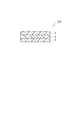
図1に示す接着シート100は、本発明の接着剤組成物をフィルム状に成形した接着剤層1のみからなるものである。接着剤層1の厚みは、1〜200μmであることが好ましい。接着シート100は、例えば、幅1〜20mm程度のテープ状や、幅10〜50cm程度のシート状であってよく、その場合、好ましくは巻き芯に巻かれた状態で搬送される。これにより、接着シート100の保管や搬送が容易となる。接着シート100は、単層の接着剤層1を複数重ねて貼り合せた積層体であってもよい。
The
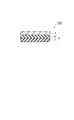
接着剤層1は、支持基材の片面又は両面に積層した構造を有する接着シートとして用いてもよい。図2に示す接着シート110は、支持基材(支持フィルム2)と、その両主面上に設けられた接着剤層1とを備える。支持フィルム2は、接着剤層1を支持する基材として機能する。支持フィルム2の片面上のみに接着剤層1が設けられていてもよい。
The
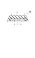
図3に示す接着シート120は、支持フィルム2と、接着剤層1と、保護フィルム3とを備えており、これらがこの順で積層されている。保護フィルム3は、接着剤層1の損傷や汚染を防ぐことを主な目的として、接着剤層1の支持フィルム2とは反対側の主面を覆うように設けられている。通常、保護フィルム3を剥離してから接着シート120がダイボンディングに用いられる。
The
接着剤層1は、本発明の接着剤組成物から得られる。以下、本発明の接着剤組成物について詳細に説明する。
The
本発明の接着剤組成物は、(A)熱可塑性樹脂と、(B)熱硬化性成分と、を含有し、上記(B)熱硬化性成分が、(B1)分子内に(メタ)アクリル基及びエポキシ基を有する反応性化合物及び/又は(B2)分子内に(メタ)アクリル基及びフェノール性水酸基を有する反応性化合物を含むものである。 The adhesive composition of the present invention contains (A) a thermoplastic resin and (B) a thermosetting component, and the (B) thermosetting component is (B1) (meth) acrylic in the molecule. A reactive compound having a group and an epoxy group and / or (B2) a reactive compound having a (meth) acrylic group and a phenolic hydroxyl group in the molecule.
接着剤層1は、本発明の接着剤組成物をフィルム状に成形してなる。接着剤層1は、半導体ウェハの保護テープ及びダイシングテープの軟化温度以下の低温で被着体に貼り付け可能であることが好ましい。貼り付け可能な温度が低いことは、半導体ウェハ反り抑制の点でも有利である。具体的には、接着剤層1を被着体に貼り付ける温度は、好ましくは10〜150℃、より好ましくは20〜100℃、更に好ましくは20〜80℃である。このような低温での貼り付けを可能にするために、接着剤層1のTgは100℃以下であることが好ましい。そのために、接着剤層1を構成する(A)熱可塑性樹脂のTgは、好ましくは100℃以下、より好ましくは−20〜80℃である。(A)熱可塑性樹脂のTgが100℃を超えると、半導体ウェハ裏面への貼り付け温度が150℃を超える可能性が高くなり、Tgが−20℃未満であると、Bステージ状態での接着剤層1表面のタック性が強くなり、取り扱い性が徐々に低下する傾向にある。
The
(A)熱可塑性樹脂に関する上記のTgは、フィルム状に成形された当該(A)熱可塑性樹脂の動的粘弾性の温度依存性を測定したときに観測される主分散のピーク温度である。(A)熱可塑性樹脂の動的粘弾性は、例えば、35mm×10mm×40μm厚の試験片を用いて、昇温速度5℃/分、周波数1Hz、測定温度−150〜300℃の条件で測定される。このとき、主分散においてtanδが極大値を示す温度(主分散温度)がTgである。粘弾性の測定は、レオメトリックス株式会社製の粘弾性アナライザー(商品名:RSA−2)を用いて行うことができる。なお、上記(A)熱可塑性樹脂とは、加熱により溶融または軟化して外力により変形流動し、冷却すると固化する線状または分岐状高分子のことであり、分子内に反応性の官能基を有するものであっても、前述のように熱流動性を有する樹脂であれば、(A)熱可塑性樹脂に含む。本発明における(A)熱可塑性樹脂は、上記動的粘弾性の1回目の測定において、Tg(tanδが極大値を示す温度(主分散温度))+100℃での貯蔵弾性率が1MPa以下となることが好ましく、0.1MPa以下となることがより好ましい。 (A) Said Tg regarding a thermoplastic resin is the peak temperature of the main dispersion | distribution observed when the temperature dependence of the dynamic viscoelasticity of the said (A) thermoplastic resin shape | molded to the film form is measured. (A) The dynamic viscoelasticity of the thermoplastic resin is measured using, for example, a test piece having a thickness of 35 mm × 10 mm × 40 μm at a temperature rising rate of 5 ° C./min, a frequency of 1 Hz, and a measurement temperature of −150 to 300 ° C. Is done. At this time, the temperature at which tan δ has a maximum value in the main dispersion (main dispersion temperature) is Tg. The measurement of viscoelasticity can be performed using a viscoelasticity analyzer (trade name: RSA-2) manufactured by Rheometrix Co., Ltd. The (A) thermoplastic resin is a linear or branched polymer that melts or softens by heating, deforms and flows by external force, and solidifies when cooled, and has a reactive functional group in the molecule. Even if it has, if it is resin which has heat fluidity as mentioned above, it will be included in (A) thermoplastic resin. In the first measurement of the dynamic viscoelasticity, (A) the thermoplastic resin in the present invention has a storage elastic modulus at Tg (temperature at which tan δ exhibits a maximum value (main dispersion temperature)) + 100 ° C. of 1 MPa or less. It is preferable that the pressure be 0.1 MPa or less.
(A)熱可塑性樹脂としては、例えば、ポリイミド樹脂、ポリアミド樹脂、ポリアミドイミド樹脂、ポリエーテルイミド樹脂、ポリウレタンイミド樹脂、ポリウレタンアミドイミド樹脂、シロキサンポリイミド樹脂、ポリエステルイミド樹脂又はそれらの共重合体の他、フェノキシ樹脂、ポリスルホン樹脂、ポリエーテルスルホン樹脂、ポリフェニレンサルファイド樹脂、ポリエステル樹脂、ポリエーテルケトン樹脂、ポリビニルアルコール樹脂、ポリビニルブチラール樹脂、スチレン−マレイミド共重合体、マレイミド−ビニル化合物共重合体、及び(メタ)アクリル共重合体からなる群から選ばれる少なくとも1種の樹脂とすることができる。ここで、(メタ)アクリル共重合体の重量平均分子量は10万〜100万の範囲にあることが好ましい。 (A) Examples of the thermoplastic resin include polyimide resins, polyamide resins, polyamideimide resins, polyetherimide resins, polyurethaneimide resins, polyurethaneamideimide resins, siloxane polyimide resins, polyesterimide resins, and copolymers thereof. , Phenoxy resin, polysulfone resin, polyethersulfone resin, polyphenylene sulfide resin, polyester resin, polyether ketone resin, polyvinyl alcohol resin, polyvinyl butyral resin, styrene-maleimide copolymer, maleimide-vinyl compound copolymer, and (meta ) At least one resin selected from the group consisting of acrylic copolymers can be used. Here, the weight average molecular weight of the (meth) acrylic copolymer is preferably in the range of 100,000 to 1,000,000.
上記樹脂群の中でも、ポリイミド樹脂が特に好ましい。ポリイミド樹脂は、1種を単独で又は必要に応じて2種以上を組み合わせて使用することができる。 Among the resin groups, polyimide resin is particularly preferable. A polyimide resin can be used individually by 1 type or in combination of 2 or more types as needed.
上記ポリイミド樹脂は、テトラカルボン酸二無水物とジアミンとを通常の方法で縮合反応させて得ることができる。例えば、テトラカルボン酸二無水物とジアミンとを有機溶媒中で縮合反応させる。通常80℃以下、好ましくは0〜60℃で付加反応を進行するにつれ反応液の粘度が徐々に上昇し、ポリイミド樹脂の前駆体であるポリアミド酸が生成する。生成したポリアミド酸を50〜80℃の温度で加熱して解重合させることによって、その分子量を調整してもよい。このポリアミド酸を脱水閉環させて、ポリイミド樹脂を得ることができる。脱水閉環は、加熱処理する熱閉環法、又は脱水剤を使用する化学閉環法により行うことができる。 The polyimide resin can be obtained by subjecting tetracarboxylic dianhydride and diamine to a condensation reaction by an ordinary method. For example, tetracarboxylic dianhydride and diamine are subjected to a condensation reaction in an organic solvent. Usually, as the addition reaction proceeds at 80 ° C. or lower, preferably 0 to 60 ° C., the viscosity of the reaction solution gradually increases, and polyamic acid, which is a polyimide resin precursor, is generated. You may adjust the molecular weight by heating and depolymerizing the produced polyamic acid at the temperature of 50-80 degreeC. This polyamic acid can be dehydrated and closed to obtain a polyimide resin. The dehydration ring closure can be performed by a thermal ring closure method in which heat treatment is performed or a chemical ring closure method using a dehydrating agent.
上記縮合反応におけるテトラカルボン酸二無水物とジアミンとの組成比は等モルであってもよいし、必要に応じてテトラカルボン酸二無水物の合計1.0molに対して、ジアミンの合計0.5〜2.0mol、好ましくは、0.8〜1.0molの範囲で組成比を調整してもよい。各成分の添加順序は任意である。テトラカルボン酸二無水物の合計1.0molに対して、ジアミンの合計が2.0molを超えると、得られるポリイミド樹脂中に、アミン末端を有するポリイミドオリゴマーの量が多くなる傾向がある。ジアミンの合計が0.5mol未満であると、酸末端を有するポリイミドオリゴマーの量が多くなる傾向がある。いずれの場合においても、ポリイミド樹脂の重量平均分子量が低くなり、接着剤組成物の耐熱性を含む種々の特性が低下する傾向がある。また、これらの末端との反応性を有するエポキシ樹脂を配合した場合、上記のポリイミドオリゴマーの量が多くなるにつれて、接着剤組成物の保存安定性が低下する傾向がある。この傾向は、特にアミン末端を有するポリイミドオリゴマーの量が多くなるにつれて顕著になる。 The composition ratio of the tetracarboxylic dianhydride and the diamine in the condensation reaction may be equimolar, and if necessary, the total of the diamine is 0.1% relative to the total 1.0 mol of the tetracarboxylic dianhydride. The composition ratio may be adjusted in the range of 5 to 2.0 mol, preferably 0.8 to 1.0 mol. The order of adding each component is arbitrary. When the total of diamines exceeds 2.0 mol with respect to the total of 1.0 mol of tetracarboxylic dianhydrides, the amount of polyimide oligomer having amine ends tends to increase in the resulting polyimide resin. There exists a tendency for the quantity of the polyimide oligomer which has an acid terminal to increase that the sum total of diamine is less than 0.5 mol. In any case, the weight average molecular weight of the polyimide resin is lowered, and various properties including heat resistance of the adhesive composition tend to be lowered. Moreover, when the epoxy resin which has the reactivity with these terminal is mix | blended, there exists a tendency for the storage stability of adhesive composition to fall as the quantity of said polyimide oligomer increases. This tendency becomes more pronounced as the amount of polyimide oligomer having amine ends increases.
テトラカルボン酸二無水物は、縮合反応の前に、その融点よりも10〜20℃低い温度で12時間以上加熱乾燥するか、又は、無水酢酸からの再結晶により精製処理されていることが好ましい。テトラカルボン酸二無水物の示差走査熱量測計(DSC)による吸熱開始温度と吸熱ピーク温度との差は、10℃以内であることが好ましい。係る温度差の値はテトラカルボン酸二無水物の純度の指標として用いることができる。吸熱開始温度及び吸熱ピーク温度は、DSC(パーキンエルマー社製、DSC−7型)を用いて、サンプル量:5mg、昇温速度:5℃/分、測定雰囲気:窒素、の条件で測定したときの値を用いる。 Before the condensation reaction, the tetracarboxylic dianhydride is preferably heated and dried at a temperature lower than its melting point by 10 to 20 ° C. for 12 hours or more, or purified by recrystallization from acetic anhydride. . The difference between the endothermic onset temperature and the endothermic peak temperature by differential scanning calorimetry (DSC) of tetracarboxylic dianhydride is preferably within 10 ° C. The value of the temperature difference can be used as an indicator of the purity of tetracarboxylic dianhydride. Endothermic start temperature and endothermic peak temperature are measured using DSC (Perkin Elmer, DSC-7 type) under the conditions of sample amount: 5 mg, heating rate: 5 ° C./min, measurement atmosphere: nitrogen. The value of is used.
ポリイミド樹脂の原料として用いられるテトラカルボン酸二無水物は、例えば、ピロメリット酸二無水物、3,3’,4,4’−ビフェニルテトラカルボン酸二無水物、2,2’,3,3’−ビフェニルテトラカルボン酸二無水物、2,2−ビス(3,4−ジカルボキシフェニル)プロパン二無水物、2,2−ビス(2,3−ジカルボキシフェニル)プロパン二無水物、1,1−ビス(2,3−ジカルボキシフェニル)エタン二無水物、1,1−ビス(3,4−ジカルボキシフェニル)エタン二無水物、ビス(2,3−ジカルボキシフェニル)メタン二無水物、ビス(3,4−ジカルボキシフェニル)メタン二無水物、ビス(3,4−ジカルボキシフェニル)スルホン二無水物、3,4,9,10−ペリレンテトラカルボン酸二無水物、ビス(3,4−ジカルボキシフェニル)エーテル二無水物、ベンゼン−1,2,3,4−テトラカルボン酸二無水物、3,4,3’,4’−ベンゾフェノンテトラカルボン酸二無水物、2,3,2’,3’−ベンゾフェノンテトラカルボン酸二無水物、3,3,3’,4’−ベンゾフェノンテトラカルボン酸二無水物、1,2,5,6−ナフタレンテトラカルボン酸二無水物、1,4,5,8−ナフタレンテトラカルボン酸二無水物、2,3,6,7−ナフタレンテトラカルボン酸二無水物、1,2,4,5−ナフタレンテトラカルボン酸二無水物、2,6−ジクロロナフタレン−1,4,5,8−テトラカルボン酸二無水物、2,7−ジクロロナフタレン−1,4,5,8−テトラカルボン酸二無水物、2,3,6,7−テトラクロロナフタレン−1,4,5,8−テトラカルボン酸二無水物、フェナンスレン−1,8,9,10−テトラカルボン酸二無水物、ピラジン−2,3,5,6−テトラカルボン酸二無水物、チオフェン−2,3,5,6−テトラカルボン酸二無水物、2,3,3’,4’−ビフェニルテトラカルボン酸二無水物、3,4,3’,4’−ビフェニルテトラカルボン酸二無水物、2,3,2’,3’−ビフェニルテトラカルボン酸二無水物、ビス(3,4−ジカルボキシフェニル)ジメチルシラン二無水物、ビス(3,4−ジカルボキシフェニル)メチルフェニルシラン二無水物、ビス(3,4−ジカルボキシフェニル)ジフェニルシラン二無水物、1,4−ビス(3,4−ジカルボキシフェニルジメチルシリル)ベンゼン二無水物、1,3−ビス(3,4−ジカルボキシフェニル)−1,1,3,3−テトラメチルジシクロヘキサン二無水物、p−フェニレンビス(トリメリテート無水物)、エチレンテトラカルボン酸二無水物、1,2,3,4−ブタンテトラカルボン酸二無水物、デカヒドロナフタレン−1,4,5,8−テトラカルボン酸二無水物、4,8−ジメチル−1,2,3,5,6,7−ヘキサヒドロナフタレン−1,2,5,6−テトラカルボン酸二無水物、シクロペンタン−1,2,3,4−テトラカルボン酸二無水物、ピロリジン−2,3,4,5−テトラカルボン酸二無水物、1,2,3,4−シクロブタンテトラカルボン酸二無水物、ビス(エキソ−ビシクロ[2,2,1]ヘプタン−2,3−ジカルボン酸二無水物、ビシクロ−[2,2,2]−オクト−7−エン−2,3,5,6−テトラカルボン酸二無水物、2,2−ビス(3,4−ジカルボキシフェニル)プロパン二無水物、2,2−ビス[4−(3,4−ジカルボキシフェニル)フェニル]プロパン二無水物、2,2−ビス(3,4−ジカルボキシフェニル)ヘキサフルオロプロパン二無水物、2,2−ビス[4−(3,4−ジカルボキシフェニル)フェニル]ヘキサフルオロプロパン二無水物、4,4’−ビス(3,4−ジカルボキシフェノキシ)ジフェニルスルフィド二無水物、1,4−ビス(2−ヒドロキシヘキサフルオロイソプロピル)ベンゼンビス(トリメリット酸無水物)、1,3−ビス(2−ヒドロキシヘキサフルオロイソプロピル)ベンゼンビス(トリメリット酸無水物)、5−(2,5−ジオキソテトラヒドロフリル)−3−メチル−3−シクロヘキセン−1,2−ジカルボン酸二無水物、テトラヒドロフラン−2,3,4,5−テトラカルボン酸二無水物、4,4’−オキシジフタル酸二無水物、4,4’−(4,4’−イソプロピリデンジフェノキシ)ビス(フタル酸二無水物)、1,2−(エチレン)ビス(トリメリテート無水物)、1,3−(トリメチレン)ビス(トリメリテート無水物)、1,4−(テトラメチレン)ビス(トリメリテート無水物)、1,5−(ペンタメチレン)ビス(トリメリテート無水物)、1,6−(ヘキサメチレン)ビス(トリメリテート無水物)、1,7−(ヘプタメチレン)ビス(トリメリテート無水物)、1,8−(オクタメチレン)ビス(トリメリテート無水物)、1,9−(ノナメチレン)ビス(トリメリテート無水物)、1,10−(デカメチレン)ビス(トリメリテート無水物)、1,12−(ドデカメチレン)ビス(トリメリテート無水物)、1,16−(ヘキサデカメチレン)ビス(トリメリテート無水物)、1,18−(オクタデカメチレン)ビス(トリメリテート無水物)から1種又は2種以上が選ばれる。これらの中でも、優れた耐湿信頼性を付与できる点で、4,4’−オキシジフタル酸二無水物、及び4,4’−(4,4’−イソプロピリデンジフェノキシ)ビス(フタル酸二無水物)が好ましい。優れた熱流動性を付与できる点で、1,10−(デカメチレン)ビス(トリメリテート無水物)、1,12−(ドデカメチレン)ビス(トリメリテート無水物)、1,16−(ヘキサデカメチレン)ビス(トリメリテート無水物)及び1,18−(オクタデカメチレン)ビス(トリメリテート無水物)が好ましい。 Examples of the tetracarboxylic dianhydride used as a raw material for the polyimide resin include pyromellitic dianhydride, 3,3 ′, 4,4′-biphenyltetracarboxylic dianhydride, 2,2 ′, 3,3. '-Biphenyltetracarboxylic dianhydride, 2,2-bis (3,4-dicarboxyphenyl) propane dianhydride, 2,2-bis (2,3-dicarboxyphenyl) propane dianhydride, 1, 1-bis (2,3-dicarboxyphenyl) ethane dianhydride, 1,1-bis (3,4-dicarboxyphenyl) ethane dianhydride, bis (2,3-dicarboxyphenyl) methane dianhydride Bis (3,4-dicarboxyphenyl) methane dianhydride, bis (3,4-dicarboxyphenyl) sulfone dianhydride, 3,4,9,10-perylenetetracarboxylic dianhydride, bis 3,4-dicarboxyphenyl) ether dianhydride, benzene-1,2,3,4-tetracarboxylic dianhydride, 3,4,3 ′, 4′-benzophenone tetracarboxylic dianhydride, 2, 3,2 ′, 3′-benzophenone tetracarboxylic dianhydride, 3,3,3 ′, 4′-benzophenone tetracarboxylic dianhydride, 1,2,5,6-naphthalene tetracarboxylic dianhydride, 1,4,5,8-naphthalenetetracarboxylic dianhydride, 2,3,6,7-naphthalenetetracarboxylic dianhydride, 1,2,4,5-naphthalenetetracarboxylic dianhydride, 2, 6-dichloronaphthalene-1,4,5,8-tetracarboxylic dianhydride, 2,7-dichloronaphthalene-1,4,5,8-tetracarboxylic dianhydride, 2,3,6,7- Tetrachloronaphthalene -1,4,5,8-tetracarboxylic dianhydride, phenanthrene-1,8,9,10-tetracarboxylic dianhydride, pyrazine-2,3,5,6-tetracarboxylic dianhydride, Thiophene-2,3,5,6-tetracarboxylic dianhydride, 2,3,3 ′, 4′-biphenyltetracarboxylic dianhydride, 3,4,3 ′, 4′-biphenyltetracarboxylic dianhydride Anhydride, 2,3,2 ′, 3′-biphenyltetracarboxylic dianhydride, bis (3,4-dicarboxyphenyl) dimethylsilane dianhydride, bis (3,4-dicarboxyphenyl) methylphenylsilane Dianhydride, bis (3,4-dicarboxyphenyl) diphenylsilane dianhydride, 1,4-bis (3,4-dicarboxyphenyldimethylsilyl) benzene dianhydride, 1,3-bis (3,4 - Carboxyphenyl) -1,1,3,3-tetramethyldicyclohexane dianhydride, p-phenylenebis (trimellitic anhydride), ethylenetetracarboxylic dianhydride, 1,2,3,4-butanetetracarboxylic acid Dianhydride, decahydronaphthalene-1,4,5,8-tetracarboxylic dianhydride, 4,8-dimethyl-1,2,3,5,6,7-hexahydronaphthalene-1,2,5 , 6-tetracarboxylic dianhydride, cyclopentane-1,2,3,4-tetracarboxylic dianhydride, pyrrolidine-2,3,4,5-tetracarboxylic dianhydride, 1,2,3 , 4-cyclobutanetetracarboxylic dianhydride, bis (exo-bicyclo [2,2,1] heptane-2,3-dicarboxylic dianhydride, bicyclo- [2,2,2] -oct-7-ene -2,3 5,6-tetracarboxylic dianhydride, 2,2-bis (3,4-dicarboxyphenyl) propane dianhydride, 2,2-bis [4- (3,4-dicarboxyphenyl) phenyl] propane Dianhydride, 2,2-bis (3,4-dicarboxyphenyl) hexafluoropropane dianhydride, 2,2-bis [4- (3,4-dicarboxyphenyl) phenyl] hexafluoropropane dianhydride 4,4′-bis (3,4-dicarboxyphenoxy) diphenyl sulfide dianhydride, 1,4-bis (2-hydroxyhexafluoroisopropyl) benzenebis (trimellitic anhydride), 1,3-bis (2-hydroxyhexafluoroisopropyl) benzenebis (trimellitic anhydride), 5- (2,5-dioxotetrahydrofuryl) -3-methyl- -Cyclohexene-1,2-dicarboxylic dianhydride, tetrahydrofuran-2,3,4,5-tetracarboxylic dianhydride, 4,4'-oxydiphthalic dianhydride, 4,4 '-(4,4 '-Isopropylidenediphenoxy) bis (phthalic dianhydride), 1,2- (ethylene) bis (trimellitic anhydride), 1,3- (trimethylene) bis (trimellitic anhydride), 1,4- (tetra Methylene) bis (trimellitic anhydride), 1,5- (pentamethylene) bis (trimellitic anhydride), 1,6- (hexamethylene) bis (trimellitic anhydride), 1,7- (heptamethylene) bis (trimellitate) Anhydride), 1,8- (octamethylene) bis (trimellitic anhydride), 1,9- (nonamethylene) bis (trimellitic anhydride), 1, 10- (Decamethylene) bis (trimellitic anhydride), 1,12- (dodecamethylene) bis (trimellitic anhydride), 1,16- (hexacamethylene) bis (trimellitic anhydride), 1,18- (octadeca One or more are selected from methylene) bis (trimellitate anhydride). Among these, 4,4′-oxydiphthalic dianhydride and 4,4 ′-(4,4′-isopropylidenediphenoxy) bis (phthalic dianhydride) are able to provide excellent moisture resistance reliability. ) Is preferred. 1,10- (Decamethylene) bis (trimellitate anhydride), 1,12- (dodecamethylene) bis (trimellitate anhydride), 1,16- (hexadecamethylene) bis in terms of imparting excellent heat fluidity (Trimellitate anhydride) and 1,18- (octadecamethylene) bis (trimellitate anhydride) are preferred.
ポリイミド樹脂の原料として用いられるジアミンは、例えば、o−フェニレンジアミン、m−フェニレンジアミン、p−フェニレンジアミン、3,3’−ジアミノジフェニルエーテル、3,4’−ジアミノジフェニルエーテル、4,4’−ジアミノジフェニルエーテル、3,3’−ジアミノジフェニルメタン、3,4’−ジアミノジフェニルメタン、4,4’−ジアミノジフェニルメタン、ビス(4−アミノ−3,5−ジメチルフェニル)メタン、ビス(4−アミノ−3,5−ジイソプロピルフェニル)メタン、3,3’−ジアミノジフェニルジフルオロメタン、3,4’−ジアミノジフェニルジフルオロメタン、4,4’−ジアミノジフェニルジフルオロメタン、3,3’−ジアミノジフェニルスルフォン、3,4’−ジアミノジフェニルスルフォン、4,4’−ジアミノジフェニルスルフォン、3,3’−ジアミノジフェニルスルフィド、3,4’−ジアミノジフェニルスルフィド、4,4’−ジアミノジフェニルスルフィド、3,3’−ジアミノジフェニルケトン、3,4’−ジアミノジフェニルケトン、4,4’−ジアミノジフェニルケトン、2,2−ビス(3−アミノフェニル)プロパン、2,2’−(3,4’−ジアミノジフェニル)プロパン、2,2−ビス(4−アミノフェニル)プロパン、2,2−ビス(3−アミノフェニル)ヘキサフルオロプロパン、2,2−(3,4’−ジアミノジフェニル)ヘキサフルオロプロパン、2,2−ビス(4−アミノフェニル)ヘキサフルオロプロパン、1,3−ビス(3−アミノフェノキシ)ベンゼン、1,4−ビス(3−アミノフェノキシ)ベンゼン、1,4−ビス(4−アミノフェノキシ)ベンゼン、3,3’−(1,4−フェニレンビス(1−メチルエチリデン))ビスアニリン、3,4’−(1,4−フェニレンビス(1−メチルエチリデン))ビスアニリン、4,4’−(1,4−フェニレンビス(1−メチルエチリデン))ビスアニリン、2,2−ビス(4−(3−アミノフェノキシ)フェニル)プロパン、2,2−ビス(4−(3−アミノフェノキシ)フェニル)ヘキサフルオロプロパン、2,2−ビス(4−(4−アミノフェノキシ)フェニル)ヘキサフルオロプロパン、ビス(4−(3−アミノフェノキシ)フェニル)スルフィド、ビス(4−(4−アミノフェノキシ)フェニル)スルフィド、ビス(4−(3−アミノフェノキシ)フェニル)スルフォン、ビス(4−(4−アミノフェノキシ)フェニル)スルフォン、3,3’−ジヒドロキシ−4,4’−ジアミノビフェニル、3,5−ジアミノ安息香酸等の芳香族ジアミン、1,3−ビス(アミノメチル)シクロヘキサン、2,2−ビス(4−アミノフェノキシフェニル)プロパン、4,7,10−トリオキサトリデカン−1,13−ジアミン、4,9−ジオキサデカン−1,12−ジアミンの他、サンテクノケミカル(株)製ジェファーミン D−230,D−400,D−2000,D−4000,ED−600,ED−900,ED−2001,EDR−148,BASF株式会社製ポリエーテルアミンD−230,D−400,D−2000等のポリオキシアルキレンジアミン等の脂肪族ジアミン、さらに1,2−ジアミノエタン、1,3−ジアミノプロパン、1,4−ジアミノブタン、1,5−ジアミノペンタン、1,6−ジアミノヘキサン、1,7−ジアミノヘプタン、1,8−ジアミノオクタン、1,9−ジアミノノナン、1,10−ジアミノデカン、1,11−ジアミノウンデカン、1,12−ジアミノドデカン、1,2−ジアミノシクロヘキサンなどの脂肪族ジアミン、さらに、1,1,3,3−テトラメチル−1,3−ビス(4−アミノフェニル)ジシロキサン、1,1,3,3−テトラフェノキシ−1,3−ビス(4−アミノエチル)ジシロキサン、1,1,3,3−テトラフェニル−1,3−ビス(2−アミノエチル)ジシロキサン、1,1,3,3−テトラフェニル−1,3−ビス(3−アミノプロピル)ジシロキサン、1,1,3,3−テトラメチル−1,3−ビス(2−アミノエチル)ジシロキサン、1,1,3,3−テトラメチル−1,3−ビス(3−アミノプロピル)ジシロキサン、1,1,3,3−テトラメチル−1,3−ビス(3−アミノブチル)ジシロキサン、1,3−ジメチル−1,3−ジメトキシ−1,3−ビス(4−アミノブチル)ジシロキサン、1,1,3,3,5,5−ヘキサメチル−1,5−ビス(4−アミノフェニル)トリシロキサン、1,1,5,5−テトラフェニル−3,3−ジメチル−1,5−ビス(3−アミノプロピル)トリシロキサン、1,1,5,5−テトラフェニル−3,3−ジメトキシ−1,5−ビス(4−アミノブチル)トリシロキサン、1,1,5,5−テトラフェニル−3,3−ジメトキシ−1,5−ビス(5−アミノペンチル)トリシロキサン、1,1,5,5−テトラメチル−3,3−ジメトキシ−1,5−ビス(2−アミノエチル)トリシロキサン、1,1,5,5−テトラメチル−3,3−ジメトキシ−1,5−ビス(4−アミノブチル)トリシロキサン、1,1,5,5−テトラメチル−3,3−ジメトキシ−1,5−ビス(5−アミノペンチル)トリシロキサン、1,1,3,3,5,5−ヘキサメチル−1,5−ビス(3−アミノプロピル)トリシロキサン、1,1,3,3,5,5−ヘキサエチル−1,5−ビス(3−アミノプロピル)トリシロキサン、1,1,3,3,5,5−ヘキサプロピル−1,5−ビス(3−アミノプロピル)トリシロキサンなどのシロキサンジアミンから選ばれる。これらのジアミンは、1種を単独で又は2種以上を組み合わせて使用することができる。 Examples of the diamine used as a raw material for the polyimide resin include o-phenylenediamine, m-phenylenediamine, p-phenylenediamine, 3,3′-diaminodiphenyl ether, 3,4′-diaminodiphenyl ether, and 4,4′-diaminodiphenyl ether. 3,3′-diaminodiphenylmethane, 3,4′-diaminodiphenylmethane, 4,4′-diaminodiphenylmethane, bis (4-amino-3,5-dimethylphenyl) methane, bis (4-amino-3,5- Diisopropylphenyl) methane, 3,3′-diaminodiphenyldifluoromethane, 3,4′-diaminodiphenyldifluoromethane, 4,4′-diaminodiphenyldifluoromethane, 3,3′-diaminodiphenylsulfone, 3,4′-diamino Diphenyl Ruphone, 4,4'-diaminodiphenylsulfone, 3,3'-diaminodiphenyl sulfide, 3,4'-diaminodiphenyl sulfide, 4,4'-diaminodiphenyl sulfide, 3,3'-diaminodiphenyl ketone, 3,4 '-Diaminodiphenyl ketone, 4,4'-diaminodiphenyl ketone, 2,2-bis (3-aminophenyl) propane, 2,2'-(3,4'-diaminodiphenyl) propane, 2,2-bis ( 4-aminophenyl) propane, 2,2-bis (3-aminophenyl) hexafluoropropane, 2,2- (3,4'-diaminodiphenyl) hexafluoropropane, 2,2-bis (4-aminophenyl) Hexafluoropropane, 1,3-bis (3-aminophenoxy) benzene, 1,4-bis (3-a Nophenoxy) benzene, 1,4-bis (4-aminophenoxy) benzene, 3,3 ′-(1,4-phenylenebis (1-methylethylidene)) bisaniline, 3,4 ′-(1,4-phenylene) Bis (1-methylethylidene)) bisaniline, 4,4 ′-(1,4-phenylenebis (1-methylethylidene)) bisaniline, 2,2-bis (4- (3-aminophenoxy) phenyl) propane, 2 , 2-bis (4- (3-aminophenoxy) phenyl) hexafluoropropane, 2,2-bis (4- (4-aminophenoxy) phenyl) hexafluoropropane, bis (4- (3-aminophenoxy) phenyl ) Sulfide, bis (4- (4-aminophenoxy) phenyl) sulfide, bis (4- (3-aminophenoxy) phenyl) sulfur , Aromatic diamines such as bis (4- (4-aminophenoxy) phenyl) sulfone, 3,3′-dihydroxy-4,4′-diaminobiphenyl, 3,5-diaminobenzoic acid, 1,3-bis ( Aminomethyl) cyclohexane, 2,2-bis (4-aminophenoxyphenyl) propane, 4,7,10-trioxatridecane-1,13-diamine, 4,9-dioxadecane-1,12-diamine, Jeffermin D-230, D-400, D-2000, D-4000, ED-600, ED-900, ED-2001, EDR-148, manufactured by Sun Techno Chemical Co., Ltd. Polyetheramine D-230 manufactured by BASF Corporation , D-400, D-2000, and other aliphatic diamines such as polyoxyalkylene diamines, and 1,2-diaminoe 1,3-diaminopropane, 1,4-diaminobutane, 1,5-diaminopentane, 1,6-diaminohexane, 1,7-diaminoheptane, 1,8-diaminooctane, 1,9-diaminononane, Aliphatic diamines such as 1,10-diaminodecane, 1,11-diaminoundecane, 1,12-diaminododecane, 1,2-diaminocyclohexane, and 1,1,3,3-tetramethyl-1,3- Bis (4-aminophenyl) disiloxane, 1,1,3,3-tetraphenoxy-1,3-bis (4-aminoethyl) disiloxane, 1,1,3,3-tetraphenyl-1,3- Bis (2-aminoethyl) disiloxane, 1,1,3,3-tetraphenyl-1,3-bis (3-aminopropyl) disiloxane, 1,1,3,3-tetramethyl Til-1,3-bis (2-aminoethyl) disiloxane, 1,1,3,3-tetramethyl-1,3-bis (3-aminopropyl) disiloxane, 1,1,3,3-tetra Methyl-1,3-bis (3-aminobutyl) disiloxane, 1,3-dimethyl-1,3-dimethoxy-1,3-bis (4-aminobutyl) disiloxane, 1,1,3,3 5,5-hexamethyl-1,5-bis (4-aminophenyl) trisiloxane, 1,1,5,5-tetraphenyl-3,3-dimethyl-1,5-bis (3-aminopropyl) trisiloxane 1,1,5,5-tetraphenyl-3,3-dimethoxy-1,5-bis (4-aminobutyl) trisiloxane, 1,1,5,5-tetraphenyl-3,3-dimethoxy-1 , 5-Bis (5-aminopentyl) to Siloxane, 1,1,5,5-tetramethyl-3,3-dimethoxy-1,5-bis (2-aminoethyl) trisiloxane, 1,1,5,5-tetramethyl-3,3-dimethoxy- 1,5-bis (4-aminobutyl) trisiloxane, 1,1,5,5-tetramethyl-3,3-dimethoxy-1,5-bis (5-aminopentyl) trisiloxane, 1,1,3 , 3,5,5-hexamethyl-1,5-bis (3-aminopropyl) trisiloxane, 1,1,3,3,5,5-hexaethyl-1,5-bis (3-aminopropyl) trisiloxane 1,1,3,3,5,5-hexapropyl-1,5-bis (3-aminopropyl) trisiloxane and other siloxane diamines. These diamines can be used alone or in combination of two or more.
ポリイミド樹脂のTgを100℃以下とするためには、ポリオキシアルキレンジアミン等の脂肪族ジアミンを用いることが好ましい。脂肪族ジアミンのジアミン全量に対する比率は1〜80モル%であることが好ましく、5〜60モル%であることがより好ましい。脂肪族ジアミンの比率が1モル%未満であると、低温貼付性、熱時動性を付与することが困難になる傾向にあり、80モル%を超えると、ポリイミド樹脂のTgが過度に低くなって、接着剤組成物をフィルム状に成形したときの自己支持性が損なわれる可能性が高くなる。
In order to make Tg of
脂肪族ジアミンとしては、例えば、サンテクノケミカル株式会社製ジェファーミン D−230,D−400,D−2000,D−4000,ED−600,ED−900,ED−2001及びEDR−148,BASF株式会社製ポリエーテルアミンD−230,D−400及びD−2000等として市販されているポリオキシアルキレンジアミンが利用可能である。 Examples of the aliphatic diamine include Jeffamine D-230, D-400, D-2000, D-4000, ED-600, ED-900, ED-2001 and EDR-148, BASF Corporation, manufactured by Sun Techno Chemical Co., Ltd. Polyoxyalkylene diamine marketed as polyether amines D-230, D-400, D-2000, etc. can be used.
ポリイミド樹脂の重量平均分子量は10000〜200000であることが好ましく、10000〜100000であることがより好ましく、20000〜80000であることが更に好ましい。これら重量平均分子量は、高速液体クロマトグラフィー(例えば株式会社島津製作所製、商品名:C−R4A)を用いてGPCにより測定して得られる、標準ポリスチレン換算値である。 The weight average molecular weight of the polyimide resin is preferably 10,000 to 200,000, more preferably 10,000 to 100,000, and still more preferably 20,000 to 80,000. These weight average molecular weights are standard polystyrene equivalent values obtained by measurement by GPC using high performance liquid chromatography (for example, trade name: C-R4A, manufactured by Shimadzu Corporation).
重量平均分子量が上記数値範囲内にあると、接着剤層1の強度、可とう性、及びタック性がより良好なものとなる。また、適切な熱流動性も得られることから、被着体表面の段差への良好な埋込性をより十分に確保することができる。ポリイミド樹脂の重量平均分子量が10000未満であると、接着剤組成物のフィルム形成性が低下したり、接着剤層1の強度が低下する傾向がある。ポリイミド樹脂の重量平均分子量が200000を超えると、徐々に接着剤層1の熱流動性が低下する傾向や、被着体の凹凸表面に対する埋め込み性が低下する傾向がある。
When the weight average molecular weight is within the above numerical range, the strength, flexibility, and tackiness of the
ポリイミド樹脂のTg及び重量平均分子量を上記の範囲内とすることにより、接着剤層1の被着体への貼り付け温度をより低く抑えることができるだけでなく、半導体素子を半導体素子搭載用支持部材に接着固定する際の加熱温度(ダイボンディング温度)も低くすることができる。その結果、半導体素子の反りの増大をより一層顕著に抑制することができる。半導体素子搭載用支持部材が有機基板の場合、ダイボンディング時の加熱温度による上記有機基板の吸湿水分の急激な気化を抑制でき、気化によるダイボンディング材層の発泡を抑制することができる。
By setting the Tg and the weight average molecular weight of the polyimide resin within the above ranges, not only can the temperature for attaching the
本発明の接着剤組成物の(B)熱硬化性成分に含まれる、(B1)分子内に(メタ)アクリル基及びエポキシ基を有する反応性化合物とは、具体的には、グリシジルメタクリレート、グリシジルアクリレート、4−ヒドロキシブチルアクリレートグリシジルエーテル、4−ヒドロキシブチルメタクリレートグリシジルエーテルの他、例えばトリフェニルホスフィンやテトラブチルアンモニウムブロミド存在下、1分子中に少なくとも2つ以上のエポキシ基を有する多官能エポキシ樹脂と、エポキシ基1当量に対し10〜90当量%(0.1〜0.9当量)の(メタ)アクリレートとを反応させることによって得られる化合物が挙げられる。また、ジブチルスズジラウレート存在下、多官能イソシアネート化合物とヒドロキシ基含有(メタ)アクリレート及びヒドロキシ基含有エポキシ化合物を反応させる、もしくは多官能エポキシ樹脂とイソシアネート基含有(メタ)アクリレートを反応させて得られるグリシジル基含有ウレタン(メタ)アクリレート等が挙げられる。 Specific examples of the reactive compound (B1) contained in the thermosetting component (B1) of the adhesive composition of the present invention having (meth) acrylic group and epoxy group in the molecule include glycidyl methacrylate and glycidyl. In addition to acrylate, 4-hydroxybutyl acrylate glycidyl ether, 4-hydroxybutyl methacrylate glycidyl ether, for example, a polyfunctional epoxy resin having at least two epoxy groups in one molecule in the presence of triphenylphosphine or tetrabutylammonium bromide The compound obtained by making 10-90 equivalent% (0.1-0.9 equivalent) (meth) acrylate react with 1 equivalent of epoxy groups is mentioned. Also, a glycidyl group obtained by reacting a polyfunctional isocyanate compound with a hydroxy group-containing (meth) acrylate and a hydroxy group-containing epoxy compound in the presence of dibutyltin dilaurate, or reacting a polyfunctional epoxy resin with an isocyanate group-containing (meth) acrylate. Examples thereof include urethane (meth) acrylate.
上記の(B1)分子内に(メタ)アクリル基及びエポキシ基を有する反応性化合物の原料となる多官能エポキシ樹脂としては、分子内にエポキシ基を2個以上含む化合物であれば、特に限定されることはなく、例えば、ビスフェノールA型(又はAD型、S型、F型)のグリシジルエーテル、水添加ビスフェノールA型のグリシジルエーテル、エチレンオキシド付加体ビスフェノールA及び/又はF型のグリシジルエーテル、プロピレンオキシド付加体ビスフェノールA及び/又はF型のグリシジルエーテル、フェノールノボラック樹脂のグリシジルエーテル、クレゾールノボラック樹脂のグリシジルエーテル、ビスフェノールAノボラック樹脂のグリシジルエーテル、ナフタレン樹脂のグリシジルエーテル、3官能型(又は4官能型)のグリシジルエーテル、ジシクロペンタジエンフェノール樹脂のグリシジルエーテル、ダイマー酸のグリシジルエステル、3官能型(又は4官能型)のグリシジルアミン、ナフタレン樹脂のグリシジルアミン等が挙げられる。 The polyfunctional epoxy resin used as a raw material for the reactive compound having a (meth) acrylic group and an epoxy group in the (B1) molecule is not particularly limited as long as it is a compound having two or more epoxy groups in the molecule. For example, glycidyl ether of bisphenol A type (or AD type, S type, F type), glycidyl ether of water-added bisphenol A type, ethylene oxide adduct bisphenol A and / or F type glycidyl ether, propylene oxide Adduct bisphenol A and / or F glycidyl ether, glycidyl ether of phenol novolac resin, glycidyl ether of cresol novolac resin, glycidyl ether of bisphenol A novolac resin, glycidyl ether of naphthalene resin, trifunctional type The chestnut Jill ether, glycidyl ether of dicyclopentadiene phenol resin, glycidyl esters of dimer acid, 3 glycidylamine functional type (or tetrafunctional), and glycidyl amines of naphthalene resins.
本発明の接着剤組成物の熱硬化性成分に含まれる、(B2)分子内に(メタ)アクリル基及びフェノール性水酸基を有する反応性化合物とは、例えば、ヒドロキシフェニルメタクリレート、ヒドロキシフェニルアクリレートの他、フェノールノボラック樹脂、クレゾールノボラック樹脂、t−ブチルフェノールノボラック樹脂、ジシクロペンタジェンクレゾールノボラック樹脂、ジシクロペンタジェンフェノールノボラック樹脂、キシリレン変性フェノールノボラック樹脂、ナフトール系化合物、トリスフェノール系化合物、テトラキスフェノールノボラック樹脂、ビスフェノールAノボラック樹脂、ポリ−p−ビニルフェノール樹脂、フェノールアラルキル樹脂など、分子内に少なくとも2個のフェノール性水酸基を有するフェノール系化合物と、グリシジルメタクリレート、グリシジルアクリレート、4−ヒドロキシブチルアクリレートグリシジルエーテル、4−ヒドロキシブチルメタクリレートグリシジルエーテルなどの(B1)分子内に(メタ)アクリル基及びエポキシ基を有する化合物とを、トリブチルアミンなどの触媒、及びハイドロキノンなどの重合禁止剤の存在下で反応させることによって得られる化合物が挙げられる。 The reactive compound having (B2) molecule having (meth) acrylic group and phenolic hydroxyl group contained in the thermosetting component of the adhesive composition of the present invention includes, for example, hydroxyphenyl methacrylate and hydroxyphenyl acrylate. Phenol novolak resin, cresol novolak resin, t-butylphenol novolak resin, dicyclopentagen cresol novolak resin, dicyclopentagen phenol novolak resin, xylylene-modified phenol novolak resin, naphthol compound, trisphenol compound, tetrakisphenol novolak resin Such as bisphenol A novolak resin, poly-p-vinylphenol resin, phenol aralkyl resin, etc., having at least two phenolic hydroxyl groups in the molecule (B1) a compound having a (meth) acryl group and an epoxy group in the molecule, such as glycidyl methacrylate, glycidyl acrylate, 4-hydroxybutyl acrylate glycidyl ether, 4-hydroxybutyl methacrylate glycidyl ether, The compound obtained by making it react in presence of a polymerization inhibitor, such as a catalyst and hydroquinone, is mentioned.
本発明において用いる上記の(B1)分子内に(メタ)アクリル基及びエポキシ基を有する反応性化合物、及び上記の(B2)分子内に(メタ)アクリル基及びフェノール性水酸基を有する反応性化合物の好ましい形態としては、分子内に含まれる(メタ)アクリル基、及びエポキシ基またはフェノール性水酸基の数が、それぞれ3個以下であることが好ましく、中でも(メタ)アクリル基の数が2個以下であることがより好ましい。このような化合物の好ましい構造として下記一般式(1)及び(2)で表される化合物が挙げられる。これらの化合物を配合することにより、後述する(B3)エポキシ樹脂及び/又は(B4)(メタ)アクリレートなどの熱硬化性成分を含む接着剤組成物の系内相溶性を向上させ、熱硬化後の靭性の高い接着剤組成物が得られる。

式中、R1、R6、R8、R10は、それぞれ、グリシジルエーテル基、または水酸基を示し、R2及びR3は2価の有機基、R4は水素原子またはメチル基、R5、R7、及びR9は、それぞれ、グリシジルエーテル基、水酸基、(メタ)アクリル基、水素原子、またはメチル基を有する有機基を示し、nは1〜15の整数を示す。
The reactive compound having (meth) acrylic group and epoxy group in the above-mentioned (B1) molecule used in the present invention, and the reactive compound having (meth) acrylic group and phenolic hydroxyl group in the above-mentioned (B2) molecule. As a preferred form, the number of (meth) acrylic groups, epoxy groups or phenolic hydroxyl groups contained in the molecule is preferably 3 or less, and among them, the number of (meth) acrylic groups is 2 or less. More preferably. Preferred structures of such compounds include compounds represented by the following general formulas (1) and (2). By blending these compounds, the in-system compatibility of the adhesive composition containing a thermosetting component such as (B3) epoxy resin and / or (B4) (meth) acrylate described later is improved, and after thermosetting An adhesive composition having high toughness can be obtained.
In the formula, R 1 , R 6 , R 8 and R 10 each represent a glycidyl ether group or a hydroxyl group, R 2 and R 3 are divalent organic groups, R 4 is a hydrogen atom or a methyl group, R 5 , R 7 , and R 9 each represents an organic group having a glycidyl ether group, a hydroxyl group, a (meth) acryl group, a hydrogen atom, or a methyl group, and n represents an integer of 1 to 15.
本発明において用いる上記(B1/B2)反応性化合物としては、保存安定性、接着性、低アウトガス性、耐熱・耐湿信頼性の観点から、5%重量減少温度が150℃以上であることが好ましく、180℃以上であることがさらに好ましく、200℃以上であることがさらにより好ましく、260以上℃であることが最も好ましい。5%重量減少温度が150℃を下回ると、本接着剤を用いて半導体装置などの電子部品を基板に半田付けで実装する際の高温加熱時のアウトガス(揮発成分)による発泡、又は発泡による接着剤層の破壊を抑制できなくなる可能性が高くなり、また、加熱時に発生する揮発成分による周辺材料、あるいは部材を汚染する可能性が高くなり、好ましくない。このような(B1/B2)反応性化合物は、例えば5%重量減少温度が150℃以上のエポキシ樹脂、またはフェノール系化合物を原料として得ることができる。 The (B1 / B2) reactive compound used in the present invention preferably has a 5% weight loss temperature of 150 ° C. or higher from the viewpoints of storage stability, adhesiveness, low outgas resistance, heat resistance and moisture resistance reliability. 180 ° C. or higher is more preferable, 200 ° C. or higher is even more preferable, and 260 ° C. or higher is most preferable. If the 5% weight loss temperature falls below 150 ° C, foaming due to outgas (volatile components) during high-temperature heating when mounting electronic components such as semiconductor devices on a substrate by soldering using this adhesive, or adhesion by foaming There is a high possibility that the destruction of the agent layer cannot be suppressed, and there is a high possibility that the surrounding materials or members due to the volatile components generated during heating will be contaminated. Such a (B1 / B2) reactive compound can be obtained using, for example, an epoxy resin having a 5% weight loss temperature of 150 ° C. or higher, or a phenol-based compound as a raw material.
さらに、本発明において用いる上記(B1/B2)反応性化合物としては、不純物イオンであるアルカリ金属イオン、アルカリ土類金属イオン、ハロゲンイオン、特には塩素イオンや加水分解性塩素等を1000ppm以下に低減した純度の高い化合物を用いることが、エレクトロマイグレーション防止や金属導体回路の腐食防止の観点から好ましい。このような化合物を得るためには、例えば、アルカリ金属イオン、アルカリ土類金属イオン、ハロゲンイオン等を低減したエポキシ樹脂、またはフェノール系化合物を原料として用いることで得ることができる。 Further, as the (B1 / B2) reactive compound used in the present invention, impurity metal ions such as alkali metal ions, alkaline earth metal ions, halogen ions, particularly chlorine ions and hydrolyzable chlorine are reduced to 1000 ppm or less. It is preferable to use a high purity compound from the viewpoint of preventing electromigration and corrosion of metal conductor circuits. In order to obtain such a compound, for example, it can be obtained by using, as a raw material, an epoxy resin with reduced alkali metal ions, alkaline earth metal ions, halogen ions, or the like, or a phenolic compound.
本発明の接着剤組成物において、上記(B1/B2)反応性化合物の好ましい含有量は、(A)熱可塑性樹脂100質量部に対して、1〜100質量部であり、より好ましくは、2〜70質量部であり、さらにより好ましくは、5〜40質量部である。前記含有量が100質量部を超えると、フィルム形成性が損なわれる傾向にある他、フィルム表面の粘着性が強くなり、フィルムの取り扱い性が損なわれる傾向にあり、前記含有量が1質量部未満であると、熱流動性、高接着性、及び強靭性の効果が得られなくなる傾向にあり、いずれも好ましくない。 In the adhesive composition of the present invention, the content of the (B1 / B2) reactive compound is preferably 1 to 100 parts by mass, more preferably 2 to 100 parts by mass of the (A) thermoplastic resin. It is -70 mass parts, More preferably, it is 5-40 mass parts. When the content exceeds 100 parts by mass, the film formability tends to be impaired, and the adhesiveness of the film surface becomes strong, and the handleability of the film tends to be impaired, and the content is less than 1 part by mass. When it is, it exists in the tendency for the effect of heat fluidity, high adhesiveness, and toughness to be acquired, and all are unpreferable.
上記の(B1/B2)反応性化合物の熱重合または熱硬化を促進するために、本発明の接着剤組成物には、必要に応じて熱ラジカル発生剤及び/または硬化促進剤を使用することもできる。前記熱ラジカル発生剤は、有機過酸化物であることが好ましい。該有機過酸化物としては、1分間半減期温度が120℃以上であることが好ましく、150℃以上であることがより好ましく、接着剤組成物の調製条件、塗膜温度、貼り合せ条件、硬化条件、その他プロセス条件、貯蔵安定性等を考慮して選択される。使用可能な過酸化物としては、特に限定はしないが、例えば、2,5−ジメチル−2,5−ジ(t−ブチルパーオキシへキサン)、ジクミルパーオキサイド、t−ブチルパーオキシ−2−エチルヘキサネート、t−ヘキシルパーオキシ−2−エチルヘキサネート、1,1−ビス(t−ブチルパーオキシ)−3,3,5−トリメチルシクロヘキサン、1,1−ビス(t−ヘキシルパーオキシ)−3,3,5−トリメチルシクロヘキサン、ビス(4−t−ブチルシクロヘキシル)パーオキシジカーボネートなどが挙げられ、これらのうちの1種を単独で、又は2種以上を混合して用いることができる。 In order to accelerate the thermal polymerization or thermal curing of the (B1 / B2) reactive compound, a thermal radical generator and / or a curing accelerator may be used in the adhesive composition of the present invention as necessary. You can also. The thermal radical generator is preferably an organic peroxide. The organic peroxide preferably has a one-minute half-life temperature of 120 ° C. or higher, more preferably 150 ° C. or higher. Preparation conditions of the adhesive composition, coating film temperature, bonding conditions, curing It is selected in consideration of conditions, other process conditions, storage stability and the like. Although it does not specifically limit as a peroxide which can be used, For example, 2,5-dimethyl-2,5-di (t-butylperoxyhexane), dicumyl peroxide, t-butylperoxy-2 -Ethyl hexanate, t-hexyl peroxy-2-ethyl hexanate, 1,1-bis (t-butylperoxy) -3,3,5-trimethylcyclohexane, 1,1-bis (t-hexyl peroxy) ) -3,3,5-trimethylcyclohexane, bis (4-t-butylcyclohexyl) peroxydicarbonate, etc., and one of these may be used alone or in combination of two or more. it can.
前記熱ラジカル発生剤の添加量は、上記(B1/B2)反応性化合物全量に対して、0.01〜20重量%が好ましく、0.1〜10重量%がさらに好ましく、0.5〜5重量%がさらにより好ましい。0.01重量%以下であると硬化促進の効果が低下する傾向にあり、20重量%を超えると、加熱時のアウトガスが増加する傾向にある他、保存安定性が損なわれる傾向にあり、いずれも好ましくない。 The addition amount of the thermal radical generator is preferably 0.01 to 20% by weight, more preferably 0.1 to 10% by weight, and more preferably 0.5 to 5% with respect to the total amount of the (B1 / B2) reactive compound. Even more preferred is weight percent. If it is 0.01% by weight or less, the effect of curing acceleration tends to be reduced, and if it exceeds 20% by weight, outgassing during heating tends to increase, and storage stability tends to be impaired. Is also not preferable.
また、熱ラジカル発生剤は半減期温度が120℃以上の化合物であれば、特に限定はしないが、例えば、パーヘキサ25B:日油社製、2,5−ジメチル−2,5−ジ(t−ブチルパーオキシへキサン)(1分間半減期温度:180℃)、パークミルD:日油社製、ジクミルパーオキサイド(1分間半減期温度:175℃)などが挙げられる。 The thermal radical generator is not particularly limited as long as it has a half-life temperature of 120 ° C. or higher. For example, perhexa 25B: manufactured by NOF Corporation, 2,5-dimethyl-2,5-di (t- Butyl peroxyhexane) (1-minute half-life temperature: 180 ° C.), Parkmill D: manufactured by NOF Corporation, dicumyl peroxide (1-minute half-life temperature: 175 ° C.), and the like.
また、(B1)分子内に(メタ)アクリル基及びエポキシ基を有する反応性化合物を用いる場合、前記硬化促進剤としては、エポキシ基の反応を促進させるものであれば特に制限はなく、例えば、イミダゾール類、ジシアンジアミド誘導体、ジカルボン酸ジヒドラジド、トリフェニルホスフィン、テトラフェニルホスホニウムテトラフェニルボレート、2−エチル−4−メチルイミダゾール−テトラフェニルボレート、1,8−ジアザビシクロ[5.4.0]ウンデセン−7−テトラフェニルボレート等が挙げられる。 In addition, when a reactive compound having a (meth) acryl group and an epoxy group in the molecule (B1) is used, the curing accelerator is not particularly limited as long as it accelerates the reaction of the epoxy group. Imidazoles, dicyandiamide derivatives, dicarboxylic acid dihydrazide, triphenylphosphine, tetraphenylphosphonium tetraphenylborate, 2-ethyl-4-methylimidazole-tetraphenylborate, 1,8-diazabicyclo [5.4.0] undecene-7- Examples include tetraphenylborate.
前記硬化促進剤の添加量は、上記(B1)分子内に(メタ)アクリル基及びエポキシ基を有する反応性化合物全量に対して、0.01〜20重量%が好ましく、0.05〜10重量%がさらに好ましく、0.1〜5重量%がさらにより好ましい。0.01重量%以下であると硬化促進の効果が低下する傾向にあり、20重量%を超えると、加熱時のアウトガスが増加する傾向にある他、保存安定性が損なわれる傾向にあり、いずれも好ましくない。 The addition amount of the curing accelerator is preferably 0.01 to 20% by weight, preferably 0.05 to 10% by weight based on the total amount of the reactive compound having (meth) acrylic group and epoxy group in the (B1) molecule. % Is more preferable, and 0.1 to 5% by weight is even more preferable. If it is 0.01% by weight or less, the effect of curing acceleration tends to be reduced, and if it exceeds 20% by weight, outgassing during heating tends to increase, and storage stability tends to be impaired. Is also not preferable.
さらに、保存安定性、プロセス適応性、酸化防止性を付与するために、本発明の接着剤組成物には、重合禁止剤及び酸化防止剤として予めキノン類、多価フェノール類、フェノール類、ホスファイト類、イオウ類等の重合禁止剤及び酸化防止剤を、接着剤層1の硬化性を損なわない範囲で添加してもよい。
Furthermore, in order to impart storage stability, process adaptability, and antioxidant properties, the adhesive composition of the present invention includes quinones, polyhydric phenols, phenols, phosphates as polymerization inhibitors and antioxidants in advance. You may add polymerization inhibitors and antioxidants, such as phytes and sulfurs, in the range which does not impair the sclerosis | hardenability of the
本発明の接着剤組成物の(B)熱硬化性成分としては、さらに(B3)エポキシ樹脂を含むことが好ましい。このような(B3)エポキシ樹脂としては、(メタ)アクリル基を有しておらず、分子内に少なくとも2個のエポキシ基を有する化合物を含むことが好ましい。硬化性や硬化物特性の点からフェノールのグリシジルエーテル型のエポキシ樹脂が極めて好ましい。このような樹脂としては、例えば、ビスフェノールA型(又はAD型、S型、F型)のグリシジルエーテル、水添加ビスフェノールA型のグリシジルエーテル、エチレンオキシド付加体ビスフェノールA型のグリシジルエーテル、プロピレンオキシド付加体ビスフェノールA型のグリシジルエーテル、フェノールノボラック樹脂のグリシジルエーテル、クレゾールノボラック樹脂のグリシジルエーテル、ビスフェノールAノボラック樹脂のグリシジルエーテル、ナフタレン樹脂のグリシジルエーテル、トリスフェノールメタン型などの3官能型(又は4官能型)のグリシジルエーテル、ジシクロペンタジエンフェノール樹脂のグリシジルエーテル、ダイマー酸のグリシジルエステル、3官能型(又は4官能型)のグリシジルアミン、ナフタレン樹脂のグリシジルアミン等が挙げられる。これらは1種を単独で又は2種以上を組み合わせて使用することができる。 The (B) thermosetting component of the adhesive composition of the present invention preferably further comprises (B3) an epoxy resin. Such (B3) epoxy resin preferably contains a compound having no (meth) acryl group and having at least two epoxy groups in the molecule. From the viewpoint of curability and cured product characteristics, phenol glycidyl ether type epoxy resin is very preferable. Examples of such resins include bisphenol A type (or AD type, S type, and F type) glycidyl ether, water-added bisphenol A type glycidyl ether, ethylene oxide adduct bisphenol A type glycidyl ether, and propylene oxide adduct. Trifunctional type (or tetrafunctional type) such as bisphenol A type glycidyl ether, phenol novolac resin glycidyl ether, cresol novolac resin glycidyl ether, bisphenol A novolac resin glycidyl ether, naphthalene resin glycidyl ether, trisphenolmethane type Glycidyl ether, glycidyl ether of dicyclopentadiene phenol resin, glycidyl ester of dimer acid, trifunctional (or tetrafunctional) glycidylamine, naphthalene Glycidyl amines resins. These can be used individually by 1 type or in combination of 2 or more types.
(B3)エポキシ樹脂は、不純物イオンである、アルカリ金属イオン、アルカリ土類金属イオン、ハロゲンイオン、特に塩素イオンや加水分解性塩素等を300ppm以下に低減した高純度品であることが、エレクトロマイグレーション防止や金属導体回路の腐食防止のために好ましい。 (B3) The epoxy resin is a high-purity product in which the impurity ions, alkali metal ions, alkaline earth metal ions, halogen ions, particularly chlorine ions and hydrolyzable chlorine are reduced to 300 ppm or less. This is preferable for prevention of corrosion and corrosion of metal conductor circuits.
必要に応じて、(B3)エポキシ樹脂にエポキシ樹脂用硬化剤を組み合わせて使用することもできる。エポキシ樹脂用硬化剤としては、例えば、フェノール系化合物、脂肪族アミン、脂環族アミン、芳香族ポリアミン、ポリアミド、脂肪族酸無水物、脂環族酸無水物、芳香族酸無水物、ジシアンジアミド、有機酸ジヒドラジド、三フッ化ホウ素アミン錯体、イミダゾール類、第3級アミン等が挙げられる。これらの中でもフェノール系化合物が好ましく、分子中に少なくとも2個のフェノール性水酸基を有するフェノール系化合物がより好ましい。このような化合物としては、例えばフェノールノボラック樹脂、クレゾールノボラック樹脂、t−ブチルフェノールノボラック樹脂、ジシクロペンタジェンクレゾールノボラック樹脂、ジシクロペンタジェンフェノールノボラック樹脂、キシリレン変性フェノールノボラック樹脂、ナフトール系化合物、トリスフェノール系化合物、テトラキスフェノールノボラック樹脂、ビスフェノールAノボラック樹脂、ポリ−p−ビニルフェノール樹脂、フェノールアラルキル樹脂等が挙げられる。これらの中でも、数平均分子量が400〜1500の範囲内のものが好ましい。これらのエポキシ樹脂用硬化剤を用いることにより、半導体装置組立加熱時に、半導体素子又は装置等の汚染の原因となるアウトガスを有効に低減できる。なお、硬化物の耐熱性を確保するためにも、これらのフェノール系化合物の配合量は、(B3)エポキシ樹脂のエポキシ当量と、フェノール系化合物のOH当量との当量比が、0.95:1.05〜1.05:0.95となるように調整することが好ましい。 If necessary, the epoxy resin (B3) can be used in combination with an epoxy resin curing agent. Examples of epoxy resin curing agents include phenolic compounds, aliphatic amines, alicyclic amines, aromatic polyamines, polyamides, aliphatic acid anhydrides, alicyclic acid anhydrides, aromatic acid anhydrides, dicyandiamide, Examples include organic acid dihydrazide, boron trifluoride amine complex, imidazoles, and tertiary amines. Among these, phenol compounds are preferable, and phenol compounds having at least two phenolic hydroxyl groups in the molecule are more preferable. Examples of such compounds include phenol novolak resins, cresol novolak resins, t-butylphenol novolak resins, dicyclopentagencresol novolak resins, dicyclopentagen phenol novolak resins, xylylene-modified phenol novolak resins, naphthol compounds, trisphenols. Examples thereof include tetrakisphenol novolac resin, bisphenol A novolac resin, poly-p-vinylphenol resin, and phenol aralkyl resin. Among these, those having a number average molecular weight in the range of 400 to 1500 are preferable. By using these epoxy resin curing agents, it is possible to effectively reduce outgas, which causes contamination of semiconductor elements or devices, during assembly heating of the semiconductor device. In order to secure the heat resistance of the cured product, the blending amount of these phenolic compounds is such that the equivalent ratio of the epoxy equivalent of (B3) epoxy resin and the OH equivalent of the phenolic compound is 0.95: It is preferable to adjust so that it may become 1.05-1.05: 0.95.
必要に応じて、前記した硬化促進剤を使用することもできる。該硬化促進剤の添加量は、(B3)エポキシ樹脂全量に対して、0.01〜20重量%が好ましく、0.05〜10重量%がさらに好ましく、0.1〜5重量%がさらにより好ましい。0.01重量%以下であると硬化促進の効果が低下する傾向にあり、20重量%を超えると、加熱時のアウトガスが増加する傾向にある他、保存安定性が損なわれる傾向にあり、いずれも好ましくない。 If necessary, the above-described curing accelerator can also be used. The addition amount of the curing accelerator is preferably 0.01 to 20% by weight, more preferably 0.05 to 10% by weight, even more preferably 0.1 to 5% by weight, based on the total amount of the (B3) epoxy resin. preferable. If it is 0.01% by weight or less, the effect of curing acceleration tends to be reduced, and if it exceeds 20% by weight, outgassing during heating tends to increase, and storage stability tends to be impaired. Is also not preferable.
本発明の接着剤組成物の(B)熱硬化性成分としては、さらに(B4)(メタ)アクリレート((B1)及び(B2)と化学構造が異なるものに限る)を含むことが好ましい。このようなアクリレートとしては、分子内に2個以上の(メタ)アクリル基を有する化合物であれば特に制限は設けないが、例えばジエチレングリコールジアクリレート、トリエチレングリコールジアクリレート、テトラエチレングリコールジアクリレート、ジエチレングリコールジメタクリレート、トリエチレングリコールジメタクリレート、テトラエチレングリコールジメタクリレート、トリメチロールプロパンジアクリレート、トリメチロールプロパントリアクリレート、トリメチロールプロパンジメタクリレート、トリメチロールプロパントリメタクリレート、1,4−ブタンジオールジアクリレート、1,6−ヘキサンジオールジアクリレート、1,4−ブタンジオールジメタクリレート、1,6−ヘキサンジオールジメタクリレート、ペンタエリスリトールトリアクリレート、ペンタエリスリトールテトラアクリレート、ペンタエリスリトールトリメタクリレート、ペンタエリスリトールテトラメタクリレート、ジペンタエリスリトールヘキサアクリレート、ジペンタエリスリトールヘキサメタクリレート、スチレン、ジビニルベンゼン、4−ビニルトルエン、4−ビニルピリジン、N−ビニルピロリドン、2−ヒドロキシエチルアクリレート、2−ヒドロキシエチルメタクリレート、1,3−アクリロイルオキシ−2−ヒドロキシプロパン、1,2−メタクリロイルオキシ−2−ヒドロキシプロパン、メチレンビスアクリルアミド、N,N−ジメチルアクリルアミド、N−メチロールアクリルアミド、トリス(β−ヒドロキシエチル)イソシアヌレートのトリアクリレート、下記一般式(3)で表される化合物、ウレタンアクリレート若しくはウレタンメタクリレート、及び尿素アクリレート等が挙げられる。 The thermosetting component (B) of the adhesive composition of the present invention preferably further contains (B4) (meth) acrylate (limited to those having a different chemical structure from (B1) and (B2)). Such an acrylate is not particularly limited as long as it is a compound having two or more (meth) acryl groups in the molecule. For example, diethylene glycol diacrylate, triethylene glycol diacrylate, tetraethylene glycol diacrylate, diethylene glycol Dimethacrylate, triethylene glycol dimethacrylate, tetraethylene glycol dimethacrylate, trimethylolpropane diacrylate, trimethylolpropane triacrylate, trimethylolpropane dimethacrylate, trimethylolpropane trimethacrylate, 1,4-butanediol diacrylate, 1, 6-hexanediol diacrylate, 1,4-butanediol dimethacrylate, 1,6-hexanediol dimethacrylate Pentaerythritol triacrylate, pentaerythritol tetraacrylate, pentaerythritol trimethacrylate, pentaerythritol tetramethacrylate, dipentaerythritol hexaacrylate, dipentaerythritol hexamethacrylate, styrene, divinylbenzene, 4-vinyltoluene, 4-vinylpyridine, N -Vinylpyrrolidone, 2-hydroxyethyl acrylate, 2-hydroxyethyl methacrylate, 1,3-acryloyloxy-2-hydroxypropane, 1,2-methacryloyloxy-2-hydroxypropane, methylenebisacrylamide, N, N-dimethylacrylamide , N-methylolacrylamide, triacryle of tris (β-hydroxyethyl) isocyanurate And compounds represented by the following general formula (3), urethane acrylate or urethane methacrylate, and urea acrylate.
[式中、R11及びR12は各々独立に、水素原子又はメチル基を示し、f及びgは各々独立に、1〜20の整数を示す。]
[Wherein, R 11 and R 12 each independently represent a hydrogen atom or a methyl group, and f and g each independently represent an integer of 1 to 20. ]
これらの(B4)(メタ)アクリレートは、1種を単独で又は2種類以上を組み合わせて使用することができる。中でも、上記一般式(3)で示されるグリコール骨格を有する(メタ)アクリレートが、熱圧着性を十分に付与できる点で好ましく、ウレタン(メタ)アクリレート、イソシアヌル酸ジ(メタ)アクリレート、またはイソシアヌル酸トリ(メタ)アクリレートが、高温接着性を十分に付与できる点で好ましい。 These (B4) (meth) acrylates can be used alone or in combination of two or more. Among these, a (meth) acrylate having a glycol skeleton represented by the general formula (3) is preferable in that it can sufficiently impart thermocompression bonding properties, and urethane (meth) acrylate, isocyanuric acid di (meth) acrylate, or isocyanuric acid. Tri (meth) acrylate is preferable in that it can sufficiently provide high-temperature adhesiveness.
本発明の接着剤組成物に含まれる(B)熱硬化性成分としては、上記の(B1/B2)反応性化合物、(B3)エポキシ樹脂、及び(B4)(メタ)アクリレートの他に、熱により架橋反応を起こす熱硬化性樹脂を更に含有してもよい。このような熱硬化性樹脂としては、例えば、シアネートエステル樹脂、フェノール樹脂、ユリア樹脂、メラミン樹脂、アルキド樹脂、アクリル樹脂、不飽和ポリエステル樹脂、シリコーン樹脂、レゾルシノールホルムアルデヒド樹脂、キシレン樹脂、フラン樹脂、ポリウレタン樹脂、ケトン樹脂、トリアリルシアヌレート樹脂、ポリイソシアネート樹脂、トリス(2−ヒドロキシエチル)イソシアヌラートを含有する樹脂、トリアリルトリメリタートを含有する樹脂、シクロペンタジエンから合成された熱硬化性樹脂、芳香族ジシアナミドの三量化による熱硬化性樹脂、マレイミド化合物、アリルナジイミド化合物、ビニル化合物、アリル化合物などが挙げられる。これら熱硬化性樹脂は、1種を単独で又は2種以上を組み合わせて用いることができる。 As the (B) thermosetting component contained in the adhesive composition of the present invention, in addition to the above (B1 / B2) reactive compound, (B3) epoxy resin, and (B4) (meth) acrylate, heat A thermosetting resin that causes a crosslinking reaction may be further contained. Examples of such thermosetting resins include cyanate ester resins, phenol resins, urea resins, melamine resins, alkyd resins, acrylic resins, unsaturated polyester resins, silicone resins, resorcinol formaldehyde resins, xylene resins, furan resins, polyurethanes. Resin, ketone resin, triallyl cyanurate resin, polyisocyanate resin, resin containing tris (2-hydroxyethyl) isocyanurate, resin containing triallyl trimellitate, thermosetting resin synthesized from cyclopentadiene And thermosetting resins by trimerization of aromatic dicyanamide, maleimide compounds, allyl nadiimide compounds, vinyl compounds, allyl compounds, and the like. These thermosetting resins can be used alone or in combination of two or more.
接着剤組成物に含まれる(B)熱硬化性成分の量は、(A)熱可塑性樹脂100質量部に対して、1〜200質量部であることが好ましく、5〜100質量部であることがより好ましく、5〜50質量部であることがさらに好ましい。この含有量が200質量部を超えると、加熱時のアウトガスが多くなる他、フィルム形成性(靭性)が徐々に損なわれる傾向にある。この含有量が1質量部未満であると、Bステージでの熱流動性、並びに、Cステージでの耐熱性及び高温接着性を有効に付与できなくなる可能性が徐々に高くなる。 The amount of the thermosetting component (B) contained in the adhesive composition is preferably 1 to 200 parts by mass, and 5 to 100 parts by mass with respect to 100 parts by mass of (A) the thermoplastic resin. Is more preferably 5 to 50 parts by mass. When this content exceeds 200 parts by mass, outgassing during heating increases and film formability (toughness) tends to be gradually impaired. When this content is less than 1 part by mass, the possibility that the heat fluidity at the B stage, the heat resistance at the C stage and the high-temperature adhesiveness cannot be effectively imparted is gradually increased.
接着剤組成物は、(B)熱硬化性成分の硬化のために、上述した有機過酸化物の他、硬化剤、及び/又は硬化促進剤(触媒)を含有してもよい。必要に応じて硬化剤と硬化促進剤、又は触媒と助触媒を併用することができる。上記硬化剤、硬化促進剤、触媒、助触媒、及び有機過酸化物の添加量、及び添加の有無については、後述する望ましい熱時の流動性、硬化性、及び硬化後の耐熱性を確保できる範囲で判断、調整する。 The adhesive composition may contain a curing agent and / or a curing accelerator (catalyst) in addition to the organic peroxide described above for curing the thermosetting component (B). If necessary, a curing agent and a curing accelerator, or a catalyst and a promoter can be used in combination. About the addition amount of the said hardening | curing agent, hardening accelerator, a catalyst, a co-catalyst, and an organic peroxide, and the presence or absence of addition, the fluidity | liquidity at the time of heat, sclerosis | hardenability mentioned later, and heat resistance after hardening can be ensured. Judge and adjust by range.
接着剤組成物は、さらに(C)フィラーを含有することが好ましい。(C)フィラーとしては、例えば、銀粉、金粉、銅粉、ニッケル粉等の金属フィラー、アルミナ、水酸化アルミニウム、水酸化マグネシウム、炭酸カルシウム、炭酸マグネシウム、ケイ酸カルシウム、ケイ酸マグネシウム、酸化カルシウム、酸化マグネシウム、酸化アルミニウム、窒化アルミニウム、結晶性シリカ、非晶性シリカ、窒化ホウ素、チタニア、ガラス、酸化鉄、セラミック等の無機フィラー、カーボン、ゴム系フィラー等の有機フィラー等が挙げられる。種類・形状等にかかわらず特に制限なくフィラーを使用することができる。 The adhesive composition preferably further contains (C) a filler. (C) As filler, for example, metal filler such as silver powder, gold powder, copper powder, nickel powder, alumina, aluminum hydroxide, magnesium hydroxide, calcium carbonate, magnesium carbonate, calcium silicate, magnesium silicate, calcium oxide, Examples thereof include inorganic fillers such as magnesium oxide, aluminum oxide, aluminum nitride, crystalline silica, amorphous silica, boron nitride, titania, glass, iron oxide, and ceramics, and organic fillers such as carbon and rubber fillers. Regardless of the type and shape, the filler can be used without any particular limitation.
(C)フィラーは、所望する機能に応じて使い分けることができる。例えば、金属フィラーは、接着剤組成物に導電性、熱伝導性、チキソ性等を付与する目的で添加され、非金属無機フィラーは、接着剤層に熱伝導性、低熱膨張性、低吸湿性等を付与する目的で添加され、有機フィラーは接着剤層に靭性等を付与する目的で添加される。これら金属フィラー、無機フィラー又は有機フィラーは、1種を単独で又は2種以上を組み合わせて使用することができる。これらの中でも、半導体装置用接着材料に求められる、導電性、熱伝導性、低吸湿特性、絶縁性等を付与できる点で、金属フィラー、無機フィラー、又は絶縁性のフィラーが好ましく、無機フィラー、又は絶縁性フィラーの中では、樹脂ワニスに対する分散性が良好で、かつ、熱時の高い接着力を付与できる点で、窒化ホウ素フィラー、シリカフィラー、またはアエロジルがより好ましい。 (C) The filler can be properly used according to the desired function. For example, the metal filler is added for the purpose of imparting conductivity, thermal conductivity, thixotropy, etc. to the adhesive composition, and the nonmetallic inorganic filler is thermally conductive, low thermal expansion, low hygroscopicity to the adhesive layer. The organic filler is added for the purpose of imparting toughness to the adhesive layer. These metal fillers, inorganic fillers or organic fillers can be used singly or in combination of two or more. Among these, metal fillers, inorganic fillers, or insulating fillers are preferable in terms of being able to impart conductivity, thermal conductivity, low moisture absorption characteristics, insulation, and the like required for adhesive materials for semiconductor devices, and inorganic fillers, Alternatively, among the insulating fillers, boron nitride filler, silica filler, or aerosil is more preferable in that the dispersibility with respect to the resin varnish is good and a high adhesive force during heating can be imparted.
接着剤組成物に含まれる(C)フィラーの量は、付与する特性、又は機能に応じて決められる。フィラーの含有量は、接着剤組成物の樹脂成分とフィラーとの合計を基準として1〜40体積%であることが好ましく、5〜30体積%であることがより好ましく、5〜20体積%であることが更に好ましい。フィラーを適度に増量させることにより、フィルム表面低粘着化、及び高弾性率化が図れ、ダイシング性(ダイサー刃による切断性)、ピックアップ性(ダイシングテープとの易はく離性)、ワイヤボンディング性(超音波効率)、熱時の接着強度をより有効に向上できる。フィラーを必要以上に増量させると、低温貼付性、被着体との界面接着性、及び熱時動性に関する効果が低下し、耐リフロー性を含む信頼性の低下を招く可能性がある。そのため、フィラーの使用量は上記の範囲内に収めることが好ましい。求められる特性のバランスをとるべく、最適なフィラーの含有量を決定することが好ましい。フィラーを用いた場合の混合・混練は、通常の攪拌機、らいかい機、三本ロール、ボールミル等の分散機を適宜、組み合わせて行うことができる。 The amount of (C) filler contained in the adhesive composition is determined according to the characteristics or functions to be imparted. The content of the filler is preferably 1 to 40% by volume, more preferably 5 to 30% by volume, and 5 to 20% by volume based on the total of the resin component and the filler of the adhesive composition. More preferably it is. By appropriately increasing the amount of filler, the film surface can be reduced in adhesiveness and elastic modulus can be increased, and dicing properties (cutability with a dicer blade), pickup properties (easy peeling from dicing tape), wire bonding properties (super Sonic efficiency) and adhesive strength during heating can be improved more effectively. When the filler is increased more than necessary, the effects relating to low temperature sticking property, interfacial adhesion with the adherend, and thermal kinetics may be reduced, leading to a decrease in reliability including reflow resistance. Therefore, the amount of filler used is preferably within the above range. In order to balance the required characteristics, it is preferable to determine an optimum filler content. Mixing and kneading in the case of using a filler can be performed by appropriately combining dispersers such as a normal stirrer, a raking machine, a three-roller, and a ball mill.
本発明の接着剤組成物には、異種材料間の界面結合を良くするために、各種カップリング剤を添加することもできる。カップリング剤としては、例えば、シラン系、チタン系、アルミニウム系等が挙げられ、中でも効果が高い点で、シラン系カップリング剤が好ましい。カップリング剤の使用量は、その効果や耐熱性及びコストの面から、熱可塑性樹脂100質量部に対して、0.01〜20質量部とすることが好ましい。 Various coupling agents can be added to the adhesive composition of the present invention in order to improve interfacial bonding between different materials. Examples of the coupling agent include silane-based, titanium-based, and aluminum-based, and among them, a silane-based coupling agent is preferable because it is highly effective. It is preferable that the usage-amount of a coupling agent shall be 0.01-20 mass parts with respect to 100 mass parts of thermoplastic resins from the surface of the effect, heat resistance, and cost.
また、本発明の接着剤組成物には、イオン性不純物を吸着して、吸湿時の絶縁信頼性を良くするために、さらにイオン捕捉剤を添加することもできる。このようなイオン捕捉剤としては、特に制限はなく、例えば、トリアジンチオール化合物、ビスフェノール系還元剤等の銅がイオン化して溶け出すのを防止するための銅害防止剤として知られる化合物、ジルコニウム系、アンチモンビスマス系マグネシウムアルミニウム化合物等の無機イオン吸着剤などが挙げられる。イオン捕捉剤の使用量は、添加による効果や耐熱性、コスト等の点から、(A)熱可塑性樹脂100質量部に対して、0.01〜10質量部が好ましい。 In addition, an ion scavenger can be further added to the adhesive composition of the present invention in order to adsorb ionic impurities and improve insulation reliability during moisture absorption. Such an ion scavenger is not particularly limited. For example, a triazine thiol compound, a compound known as a copper damage preventer for preventing copper from being ionized and dissolved, such as a bisphenol-based reducing agent, a zirconium-based compound And inorganic ion adsorbents such as antimony bismuth-based magnesium aluminum compounds. The amount of the ion scavenger used is preferably 0.01 to 10 parts by mass with respect to 100 parts by mass of the thermoplastic resin (A) from the viewpoint of the effect of addition, heat resistance, cost, and the like.
さらに、接着剤組成物には、適宜、軟化剤、老化防止剤、着色剤、難燃剤、テルペン系樹脂等の粘着付与剤を添加しても良い。 Furthermore, you may add tackifiers, such as a softening agent, anti-aging agent, a coloring agent, a flame retardant, and a terpene resin, to an adhesive composition suitably.
さらに、本発明の接着剤組成物には、必要に応じて光ラジカル発生剤、光塩基発生剤、または光酸発生剤などの光開始剤を添加しても良い。これにより、本発明の接着剤組成物を、UV照射による光硬化を利用した弾性率の上昇によるダイシング性の向上、または粘着性の低減によるピックアップ性の促進などの効果を付与できる。また、アルカリ可溶性の熱可塑性樹脂を組み合わせたときの現像によるパターン形成性などの機能性を付与できる。前記光開始剤の使用量は、添加による効果や耐熱性、コスト等の点から、(A)熱可塑性樹脂100質量部に対して、0.01〜10質量部が好ましい。 Furthermore, you may add photoinitiators, such as a photoradical generator, a photobase generator, or a photoacid generator, to the adhesive composition of this invention as needed. Thereby, the adhesive composition of the present invention can be imparted with an effect such as improvement of dicing property by increasing the elastic modulus using photocuring by UV irradiation or promotion of pickup property by reducing tackiness. Moreover, functionality such as pattern formation by development when an alkali-soluble thermoplastic resin is combined can be imparted. The amount of the photoinitiator used is preferably 0.01 to 10 parts by mass with respect to 100 parts by mass of the thermoplastic resin (A) from the viewpoints of the effect of addition, heat resistance, cost, and the like.
本実施形態に係る接着シートは、例えば、接着剤組成物を有機溶媒中に溶解又は分散させたワニスを支持基材上に塗工し、塗工されたワニスを加熱乾燥して接着剤層を形成する方法により製造することができる。接着剤層の形成の後、支持基材を除去してもよいし、支持基材をそのまま接着シートの支持フィルムとして用いてもよい。加熱乾燥の条件は、ワニス中の有機溶媒が充分に揮散する条件であれば特に制限はないが、通常、50〜200℃で、0.1〜90分間程度である。 In the adhesive sheet according to the present embodiment, for example, a varnish obtained by dissolving or dispersing an adhesive composition in an organic solvent is applied onto a support substrate, and the applied varnish is heated and dried to form an adhesive layer. It can be manufactured by the forming method. After the formation of the adhesive layer, the support substrate may be removed, or the support substrate may be used as it is as a support film for the adhesive sheet. The heat drying conditions are not particularly limited as long as the organic solvent in the varnish is sufficiently volatilized, but is usually 50 to 200 ° C. and about 0.1 to 90 minutes.
接着剤層を形成するために用いられるワニスは、接着剤組成物を構成する上述の各成分を有機溶媒中で混合し、必要に応じて混合物を混練する方法により調製される。ワニスを調製するための混合及び混練は、通常の攪拌機、らいかい機、三本ロール、ボールミル等の分散機を適宜組み合わせて行うことができる。 The varnish used to form the adhesive layer is prepared by a method in which the above-mentioned components constituting the adhesive composition are mixed in an organic solvent, and the mixture is kneaded as necessary. Mixing and kneading for preparing the varnish can be performed by appropriately combining dispersers such as a normal stirrer, a raking machine, a triple roll, and a ball mill.
ワニスに用いられる有機溶媒は、各成分を均一に溶解又は分散できるものであれば特に制限はなく、例えば、ジメチルホルムアミド、ジメチルアセトアミド、N−メチル−2−ピロリドン、ジメチルスルホキシド、ジエチレングリコールジメチルエーテル、トルエン、ベンゼン、キシレン、メチルエチルケトン、メチルイソブチルケトン、テトラヒドロフラン、エチルセロソルブ、エチルセロソルブアセテート、ブチルセロソルブ、ジオキサン、シクロヘキサノン及び酢酸エチルから選ばれる。 The organic solvent used in the varnish is not particularly limited as long as each component can be uniformly dissolved or dispersed. For example, dimethylformamide, dimethylacetamide, N-methyl-2-pyrrolidone, dimethyl sulfoxide, diethylene glycol dimethyl ether, toluene, Selected from benzene, xylene, methyl ethyl ketone, methyl isobutyl ketone, tetrahydrofuran, ethyl cellosolve, ethyl cellosolve acetate, butyl cellosolve, dioxane, cyclohexanone and ethyl acetate.
接着剤層を形成するために用いられる支持基材(支持フィルム2)は、上記の加熱、乾燥条件に耐えるものであれば特に限定されるものではない。例えば、ポリエステルフィルム、ポリプロピレンフィルム、ポリエチレンテレフタレートフィルム、ポリイミドフィルム、ポリエーテルイミドフィルム、ポリエーテルナフタレートフィルム、又はメチルペンテンフィルムが用いられる。これらの基材フィルムは、2種以上を組み合わせた多層フィルムであってもよく、表面がシリコーン系、シリカ系等の離型剤などで処理されたものであってもよい。 The support substrate (support film 2) used for forming the adhesive layer is not particularly limited as long as it can withstand the heating and drying conditions described above. For example, a polyester film, a polypropylene film, a polyethylene terephthalate film, a polyimide film, a polyetherimide film, a polyether naphthalate film, or a methylpentene film is used. These base film may be a multilayer film in which two or more kinds are combined, or the surface may be treated with a release agent such as silicone or silica.
図4は、ダイシングシートを備えるダイシング・ダイボンド一体型の接着シートの一実施形態を示す断面図である。図4に示す接着シート130は、基材フィルム7及び基材フィルム上に設けられた粘着剤層6を有するダイシングシート5と、ダイシングシートの粘着剤層6上に設けられたフィルム状の接着剤層1とから構成される積層体である。図4に示す接着シート130は、ダイシングシートとダイボンディングフィルムの両者に要求される特性を兼ね備える。図4の接着シート130において用いられる基材フィルム7は、通常、上述の支持フィルム2と同様のものである。
FIG. 4 is a cross-sectional view showing an embodiment of a dicing / die bonding integrated adhesive sheet including a dicing sheet. An
図4の接着シート130の接着剤層1は、これが貼り付けられ半導体ウェハに近い形状で予め形成されている(プリカットされている)ことが好ましい。
The
粘着剤層6は、感圧型又は放射線硬化型の粘着剤によって形成されている。粘着剤層6は、ダイシング時には半導体素子が飛散しない十分な粘着力を有し、その後の半導体素子のピックアップ工程においては半導体素子を傷つけない程度の低い粘着力を有する、当該用途で通常用いられているものを使用することができる。例えば、放射線硬化型の粘着剤は、ダイシングの際には高い粘着力を有し、ダイシング後のピックアップの際にはピックアップ前の放射線照射によってその粘着力が低下する。
The pressure-
図5の接着シート140のように、粘着材層を有するダイシングシートを用いるのに代えて、ダイシングシートとしての機能を有する基材フィルム7を用いることもできる。図5の接着シート140において用いられる基材フィルム7は、引張張力が加えられたときの伸び(いわゆる“エキスパンド”)を確保できるものである。基材フィルム7としては、例えばポリオレフィンフィルムが好ましく用いられる。
Instead of using a dicing sheet having an adhesive layer as in the
図4又は図5に示される接着シート130又は140は、ダイシング時にはダイシングシートとして、ダイボンディング時にはダイボンディングフィルムとしての機能を発揮する。そのため、これら接着シート130又は140の接着剤層1を、加熱しながら半導体ウェハの裏面にラミネートし、ダイシングした後、接着剤層が貼り付けられた状態の半導体素子をピックアップして、ダイボンディングを行うことができる。
The
以上説明した本実施形態に係る接着剤組成物及び接着シートは、IC、LSI等の半導体素子を他の被着体と接着剤、言い換えるとダイボンディング用接着剤として極めて有用である。 The adhesive composition and adhesive sheet according to the present embodiment described above are extremely useful as adhesives for other adherends to semiconductor elements such as IC and LSI, in other words, as die bonding adhesives.
半導体素子が接着される被着体としては、42アロイリードフレーム、銅リードフレーム等のリードフレーム;ポリイミド樹脂、エポキシ樹脂等のプラスチックフィルム;ガラス不織布等基材にポリイミド樹脂、エポキシ樹脂等のプラスチックを含浸、硬化させたもの;アルミナ等のセラミックス等の半導体素子搭載用支持部材等がある。中でも、表面に有機レジスト層を具備してなる有機基板、表面に配線有する有機基板等の表面に凹凸を有する有機基板と半導体素子とを接着するためのダイボンディング用接着材料として接着シートが好適に用いられる。 The adherend to which the semiconductor element is bonded includes a lead frame such as a 42 alloy lead frame or a copper lead frame; a plastic film such as a polyimide resin or an epoxy resin; and a plastic such as a polyimide resin or an epoxy resin on a substrate such as a glass nonwoven fabric. Impregnated and hardened; semiconductor element mounting support members such as ceramics such as alumina. Among them, an adhesive sheet is suitably used as an adhesive material for die bonding for bonding an organic substrate having an uneven surface to a semiconductor element, such as an organic substrate having an organic resist layer on the surface, an organic substrate having wiring on the surface, and the like. Used.
本実施形態に係る接着剤組成物及び接着シートは、複数の半導体素子を積み重ねた構造の半導体装置(Stacked−PKG)において、隣接する半導体素子同士を接着するために用いられる半導体素子用接着剤としても好適に用いられる。 The adhesive composition and the adhesive sheet according to the present embodiment are used as an adhesive for a semiconductor element used for adhering adjacent semiconductor elements in a semiconductor device (Stacked-PKG) having a structure in which a plurality of semiconductor elements are stacked. Are also preferably used.
次に、本実施形態に係る接着剤組成物の用途に関連して、半導体素子の実施形態について図面を用いて具体的に説明する。なお、近年は様々な構造の半導体装置が提案されており、本実施形態の接着剤組成物及び接着シートの用途は、以下に説明する構造の半導体装置に限定されるものではない。 Next, in connection with the use of the adhesive composition according to the present embodiment, embodiments of the semiconductor element will be specifically described with reference to the drawings. In recent years, semiconductor devices having various structures have been proposed, and the use of the adhesive composition and the adhesive sheet of the present embodiment is not limited to the semiconductor devices having the structures described below.
図6は、半導体装置の一実施形態を示す模式断面図である。図6に示す半導体装置200は、半導体素子9が、上述のフィルム状接着剤によって形成されたダイボンディング層(硬化した接着剤層)1を介して半導体素子搭載用支持部材10に接着され、半導体素子9の接続端子(図示せず)がワイヤ11を介して外部接続端子(図示せず)と電気的に接続され、更に、封止材12によって封止された構成を有している。
FIG. 6 is a schematic cross-sectional view showing an embodiment of a semiconductor device. In a
図7は、半導体装置の別の実施形態を示す模式断面図である。図7に示す半導体装置210は、一段目の半導体素子9aが上記接着剤組成物によって形成されたダイボンディング層(硬化した接着剤層)1を介して端子13が形成された半導体素子搭載用支持部材10に接着され、半導体素子9aの上に半導体素子9bが上記接着剤組成物によって形成されたダイボンディング層(硬化した接着剤層)1を介して接着され、全体が封止材12によって封止された構成を有している。半導体素子9a及び半導体素子9bの接続端子(図示せず)は、それぞれワイヤ11を介して外部接続端子と電気的に接続されている。
FIG. 7 is a schematic cross-sectional view showing another embodiment of the semiconductor device. The
図6及び図7に示す半導体装置(半導体パッケージ)は、半導体素子と半導体素子搭載用支持部材との間にフィルム状の接着剤層を挟み、加熱圧着して両者を接着させ、その後ワイヤボンディング工程、必要に応じて封止材による封止工程等の工程を経ることにより製造することができる。上記加熱圧着工程における加熱温度は、通常、20〜250℃であり、荷重は、通常、0.01〜20kgfであり、加熱時間は、通常、0.1〜300秒間である。 The semiconductor device (semiconductor package) shown in FIGS. 6 and 7 has a film-like adhesive layer sandwiched between a semiconductor element and a semiconductor element mounting support member, and is bonded by thermocompression bonding, and then a wire bonding step. And it can manufacture by passing through processes, such as a sealing process by a sealing material, as needed. The heating temperature in the thermocompression bonding step is usually 20 to 250 ° C., the load is usually 0.01 to 20 kgf, and the heating time is usually 0.1 to 300 seconds.
以下、実施例及び比較例に基づいて本発明をより具体的に説明するが、本発明は以下の実施例に限定されるものではない。 EXAMPLES Hereinafter, although this invention is demonstrated more concretely based on an Example and a comparative example, this invention is not limited to a following example.
[ポリイミド樹脂(PI−1)の合成]
温度計、攪拌機、冷却管、及び窒素流入管を装着した300mLフラスコ中に、1,3−ビス(3−アミノプロピル)テトラメチルジシロキサン(信越化学工業株式会社製、商品名:LP−7100)12.42g、ポリオキシプロピレンジアミン(BASF株式会社製、商品名:D400、分子量:452.4)22.62g、及び、N−メチル−2−ピロリドン140gを仕込んで攪拌して、反応液を調製した。ジアミンが溶解した後、フラスコを氷浴中で冷却しながら、予め無水酢酸からの再結晶により精製した4,4’−オキシジフタル酸二無水物32.62gを反応液に少量ずつ添加した。室温(25℃)で8時間反応させた後、キシレン80.5gを加え、窒素ガスを吹き込みながら180℃で加熱することにより、水と共にキシレンを共沸除去してポリイミド樹脂(PI−1)を含むワニスを得た。得られたポリイミド樹脂(PI−1)の分子量をGPCにより測定したところ、ポリスチレン換算で、数平均分子量Mn=14000、重量平均分子量Mw=35000であった。また、得られたポリイミド樹脂(PI−1)のTgは45℃であった。
[Synthesis of Polyimide Resin (PI-1)]
1,3-bis (3-aminopropyl) tetramethyldisiloxane (manufactured by Shin-Etsu Chemical Co., Ltd., trade name: LP-7100) in a 300 mL flask equipped with a thermometer, stirrer, condenser, and nitrogen inflow pipe 12.42 g, polyoxypropylene diamine (manufactured by BASF Corporation, trade name: D400, molecular weight: 452.4) 22.62 g and N-methyl-2-pyrrolidone 140 g were charged and stirred to prepare a reaction solution. did. After the diamine was dissolved, 32.62 g of 4,4′-oxydiphthalic dianhydride purified in advance by recrystallization from acetic anhydride was added to the reaction solution little by little while the flask was cooled in an ice bath. After reacting at room temperature (25 ° C.) for 8 hours, 80.5 g of xylene was added, and heated at 180 ° C. while blowing nitrogen gas to azeotropically remove xylene together with water to remove the polyimide resin (PI-1). A varnish containing was obtained. When the molecular weight of the obtained polyimide resin (PI-1) was measured by GPC, it was number average molecular weight Mn = 14000 and weight average molecular weight Mw = 35000 in terms of polystyrene. Moreover, Tg of the obtained polyimide resin (PI-1) was 45 degreeC.
[ポリイミド樹脂(PI−2)の合成]
温度計、攪拌機、冷却管、及び窒素流入管を装着した300mLフラスコ中に、2,2−ビス(4−アミノフェノキシフェニル)プロパン20.52g、4,9−ジオキサデカン−1,12−ジアミン10.20g、及び、N−メチル−2−ピロリドン193.5gを仕込んで撹拌することにより、有機溶媒であるN−メチル−2−ピロリドン中に上記各ジアミンが溶解した反応液を得た。この反応液に1,10−(デカメチレン)ビス(トリメリテート二無水物)52.20gを少量ずつ添加すると共に、窒素ガスを吹き込みながら180℃で5時間加熱して反応を進行させた。このとき発生する水を系外に除去することにより、ポリイミド樹脂(PI−2)を含むワニスを得た。得られたポリイミド樹脂(PI−2)の分子量をGPCにより測定したところ、ポリスチレン換算で、数平均分子量Mn=28900、重量平均分子量Mw=88600であった。また、得られたポリイミド樹脂(PI−2)のTgは73℃であった。
[Synthesis of polyimide resin (PI-2)]
In a 300 mL flask equipped with a thermometer, stirrer, condenser, and nitrogen inlet tube, 20.52 g of 2,2-bis (4-aminophenoxyphenyl) propane, 4,9-dioxadecane-1,12-diamine. 20 g and 193.5 g of N-methyl-2-pyrrolidone were charged and stirred to obtain a reaction solution in which each diamine was dissolved in N-methyl-2-pyrrolidone as an organic solvent. To this reaction solution, 52.20 g of 1,10- (decamethylene) bis (trimellitate dianhydride) was added little by little and the reaction was allowed to proceed by heating at 180 ° C. for 5 hours while blowing nitrogen gas. By removing the water generated at this time out of the system, a varnish containing a polyimide resin (PI-2) was obtained. When the molecular weight of the obtained polyimide resin (PI-2) was measured by GPC, it was number average molecular weight Mn = 28900 and weight average molecular weight Mw = 88600 in terms of polystyrene. Moreover, Tg of the obtained polyimide resin (PI-2) was 73 degreeC.
[反応性化合物A−1の合成]
温度計、攪拌機、及び窒素流入管を装着した500mLフラスコ中に、液状のビスフェノールAビスグリシジルエーテル(東都化成製YD−825GS、エポキシ当量178g/eq)178g(1.0当量)に、アクリル酸36g(0.5当量)と、トリフェニルホスフィン0.5gと、ヒドロキノン0.15gとを加え、100℃で7時間反応させ、分子内にアクリル基及びエポキシ基を有する反応性化合物を得た。得られた化合物を平沼産業製、電位差滴定装置COM−1600を用いて、水酸化カリウムのエタノール溶液で滴定し、酸価が0.3KOHmg/g以下であることを確認した(5%重量減少温度:300℃、エポキシ基数:1、アクリル基数:1)。なお、エポキシ基数及びアクリル基数は、原料の仕込み量(当量比)から計算して得られる理論値である。
[Synthesis of Reactive Compound A-1]
In a 500 mL flask equipped with a thermometer, a stirrer, and a nitrogen inflow tube, 178 g (1.0 equivalent) of liquid bisphenol A bisglycidyl ether (YD-825GS manufactured by Tohto Kasei, epoxy equivalent 178 g / eq) and 36 g of acrylic acid (0.5 equivalent), 0.5 g of triphenylphosphine, and 0.15 g of hydroquinone were added and reacted at 100 ° C. for 7 hours to obtain a reactive compound having an acrylic group and an epoxy group in the molecule. The obtained compound was titrated with an ethanol solution of potassium hydroxide using a potentiometric titrator COM-1600 manufactured by Hiranuma Sangyo Co., Ltd. to confirm that the acid value was 0.3 KOHmg / g or less (5% weight loss temperature). : 300 ° C., number of epoxy groups: 1, number of acrylic groups: 1). In addition, the number of epoxy groups and the number of acrylic groups are theoretical values obtained by calculation from the charged amount (equivalent ratio) of raw materials.
[反応性化合物A−2の合成]
温度計、攪拌機、及び窒素流入管を装着した500mLフラスコ中に、液状のビスフェノールFビスグリシジルエーテル(大日本インキ化学製EXA830CRP、エポキシ当量160g/eq)160g(1.0当量)に、アクリル酸36g(0.5当量)と、トリフェニルホスフィン0.5gと、ハイドロキノン0.15gとを加え、100℃で7時間反応し、分子内にアクリル基及びエポキシ基を有する反応性化合物を得た。得られた化合物を上記と同様の装置を用いて、水酸化カリウムのエタノール溶液で滴定し、酸価が0.3KOHmg/g以下であることを確認した(5%重量減少温度:300℃、エポキシ基数:1、アクリル基数:1)。上記と同様、エポキシ基数及びアクリル基数は、理論値である。
[Synthesis of Reactive Compound A-2]
In a 500 mL flask equipped with a thermometer, stirrer, and nitrogen inflow tube, liquid bisphenol F bisglycidyl ether (EXA830CRP manufactured by Dainippon Ink & Chemicals, epoxy equivalent 160 g / eq) 160 g (1.0 equivalent), acrylic acid 36 g (0.5 equivalent), 0.5 g of triphenylphosphine, and 0.15 g of hydroquinone were added and reacted at 100 ° C. for 7 hours to obtain a reactive compound having an acrylic group and an epoxy group in the molecule. The obtained compound was titrated with an ethanol solution of potassium hydroxide using the same apparatus as described above, and it was confirmed that the acid value was 0.3 KOH mg / g or less (5% weight loss temperature: 300 ° C., epoxy Number of radicals: 1, number of acrylic radicals: 1). As above, the number of epoxy groups and the number of acrylic groups are theoretical values.
[反応性化合物A−3の合成]
固形のフェノールノボラック型エポキシ樹脂(東都化成社製YDPN−638、エポキシ当量174g/eq)174g(1.0当量)に、アクリル酸36g(0.5当量)と、トリフェニルホスフィン0.48gと、ハイドロキノン0.10gとを加え、90℃〜100℃で7時間反応し、分子内にアクリル基及びエポキシ基を有する反応性化合物を得た。得られた化合物を上記と同様の装置を用いて、水酸化カリウムのエタノール溶液で滴定し、酸価が0.3KOHmg/g以下であることを確認した(5%重量減少温度:310℃、エポキシ基数:約1.7、アクリル基数:約1.7)。上記と同様、エポキシ基数及びアクリル基数は、理論値である。
[Synthesis of Reactive Compound A-3]
174 g (1.0 equivalent) of solid phenol novolac type epoxy resin (YDPN-638 manufactured by Tohto Kasei Co., Ltd., epoxy equivalent 174 g / eq), 36 g (0.5 equivalent) of acrylic acid, 0.48 g of triphenylphosphine, Hydroquinone 0.10g was added and it reacted at 90 to 100 degreeC for 7 hours, and the reactive compound which has an acryl group and an epoxy group in a molecule | numerator was obtained. The obtained compound was titrated with an ethanol solution of potassium hydroxide using the same apparatus as described above, and it was confirmed that the acid value was 0.3 KOH mg / g or less (5% weight loss temperature: 310 ° C., epoxy Number of groups: about 1.7, number of acrylic groups: about 1.7). As above, the number of epoxy groups and the number of acrylic groups are theoretical values.
なお、上記5%重量減少温度は、示差熱熱重量同時測定装置(エスアイアイ・ナノテクノロジー株式会社製、EXSTAR 6300)を用いて、昇温速度:10℃/分、空気流量:80mL/分、測定温度:40℃〜400℃の条件で測定を行ない、重量が5%減少した時の温度を計測して、5%重量減少温度とした。 The 5% weight reduction temperature was determined by using a differential thermothermal gravimetric simultaneous measurement apparatus (EXSTAR 6300, manufactured by SII Nano Technology Co., Ltd.), a heating rate: 10 ° C./min, an air flow rate: 80 mL / min, Measurement temperature: Measurement was performed under conditions of 40 ° C. to 400 ° C., and the temperature when the weight decreased by 5% was measured to obtain a 5% weight reduction temperature.
[反応性化合物B−1の合成]
フェノールノボラック(日立化成製H−1、OH当量106g/eq)106g(1.0当量)及びMEK(メチルエチルケトン)45.5gに、トリブチルアミン0.2g、及びハイドロキノン0.1gを添加し、110℃に加熱した。この反応液中にグリシジルアクリレート70g(0.5当量)を30分間で滴下した後、110℃で5時間攪拌反応させ、不揮発分80%のアクリル基含有フェノールノボラック(アクリル基変性率50%)を得た。上記と同様、アクリル基変性率は、理論値である。
[Synthesis of Reactive Compound B-1]
To 106 g (1.0 equivalent) of phenol novolak (Hitachi Chemical Co., Ltd., OH equivalent 106 g / eq) and 45.5 g of MEK (methyl ethyl ketone), 0.2 g of tributylamine and 0.1 g of hydroquinone were added, and 110 ° C. Heated. In this reaction solution, 70 g (0.5 equivalent) of glycidyl acrylate was added dropwise over 30 minutes, and the mixture was reacted with stirring at 110 ° C. for 5 hours. Obtained. As described above, the acrylic group modification rate is a theoretical value.
[接着剤組成物(ワニス)の調製]
上記で得たポリイミド樹脂(PI−1、PI−2)、反応性化合物(A−1、A−2、A−3、B−1)をそれぞれ用い、下記表1に示す組成比(単位:質量部)で各成分を配合して、接着剤層形成用のワニスを得た。
[Preparation of adhesive composition (varnish)]
Using the polyimide resins (PI-1, PI-2) and reactive compounds (A-1, A-2, A-3, B-1) obtained above, the composition ratios (unit: Each component was blended in (part by mass) to obtain a varnish for forming an adhesive layer.
なお、表1中の各成分の記号は下記のものを意味する。
<熱可塑性樹脂>
「B−74(Butvar−74)」:ソルーシア、ポリビニルブチラール樹脂(Tg:75℃、重量平均分子量:135000)
「ZX−1395」:東都化成、ビスフェノールF型フェノキシ樹脂(Tg:68℃、重量平均分子量:88000)
<エポキシ樹脂>
「ESCN195」:住友化学株式会社製、クレゾールノボラック型固体状エポキシ樹脂(エポキシ当量:200)
「YDF−8170」:東都化成、ビスフェノールF型液状エポキシ樹脂(エポキシ当量:160)
<エポキシ樹脂用硬化剤>
「HP−850N」:日立化成工業社製、フェノールノボラック(OH当量:106)
<エポキシ樹脂用硬化促進剤>
「TPPK」:東京化成工業株式会社製、テトラフェニルホスホニウムテトラフェニルボラート
<アクリレート化合物>
「R−712」:日本化薬株式会社製、エトキシ化ビスフェノールFジアクリレート
「M−313」:東亜合成株式会社製、イソシアヌル酸EO変性ジ及びトリアクリレート
<過酸化物>
パークミルD:日油株式会社製、ジクミルパーオキサイド(1分間半減期温度:175℃)
<フィラー>
「HP−P1」:水島合金鉄株式会社製、窒化ホウ素フィラー
<溶媒>
「NMP」:関東化学株式会社製、N−メチル−2−ピロリドン
In addition, the symbol of each component in Table 1 means the following.
<Thermoplastic resin>
“B-74 (Butvar-74)”: Solusia, polyvinyl butyral resin (Tg: 75 ° C., weight average molecular weight: 135000)
“ZX-1395”: Tohto Kasei, bisphenol F type phenoxy resin (Tg: 68 ° C., weight average molecular weight: 88000)
<Epoxy resin>
“ESCN195”: manufactured by Sumitomo Chemical Co., Ltd., cresol novolac type solid epoxy resin (epoxy equivalent: 200)
“YDF-8170”: Toto Kasei, bisphenol F type liquid epoxy resin (epoxy equivalent: 160)
<Curing agent for epoxy resin>
“HP-850N”: manufactured by Hitachi Chemical Co., Ltd., phenol novolak (OH equivalent: 106)
<Curing accelerator for epoxy resin>
“TPPK”: manufactured by Tokyo Chemical Industry Co., Ltd., tetraphenylphosphonium tetraphenylborate <acrylate compound>
“R-712”: Nippon Kayaku Co., Ltd., ethoxylated bisphenol F diacrylate “M-313”: Toagosei Co., Ltd., isocyanuric acid EO-modified diacrylate and triacrylate <peroxide>
Park mill D: NOF Corporation, Dicumyl peroxide (1-minute half-life temperature: 175 ° C)
<Filler>
“HP-P1”: manufactured by Mizushima Alloy Iron Co., Ltd., boron nitride filler <solvent>
“NMP”: manufactured by Kanto Chemical Co., Inc., N-methyl-2-pyrrolidone
[接着シートの調製]
得られたワニスを、乾燥後の膜厚が40μm±5μmとなるように、それぞれ支持フィルム上に塗布した。支持フィルムとして2軸延伸ポリプロピレン(OPP)フィルム(厚さ50μm)を用いた。塗布されたワニスをオーブン中にて80℃で30分間、続いて、120℃で30分間加熱することにより乾燥して、支持フィルム及び該支持フィルム上に形成されたフィルム状の接着剤層を有する接着シートを得た。
[Preparation of adhesive sheet]
The obtained varnish was apply | coated on the support film so that the film thickness after drying might be set to 40 micrometers +/- 5micrometer. A biaxially oriented polypropylene (OPP) film (thickness 50 μm) was used as the support film. The coated varnish is dried by heating in an oven at 80 ° C. for 30 minutes and then at 120 ° C. for 30 minutes to have a support film and a film-like adhesive layer formed on the support film An adhesive sheet was obtained.
[低温貼付性の評価]
実施例及び比較例で得られた各接着シートから、幅10mm、長さ40mmの試験片を切り出した。この試験片を、支持台上に載せたシリコンウェハ(6インチ径、厚さ400μm)の裏面(支持台と反対側の面)に、接着剤層がシリコンウェハ側になる向きで積層した。積層は、ロール(温度100℃、線圧4kgf/cm、送り速度0.5m/分)で加圧する方法により行った。
[Evaluation of low temperature adhesiveness]
A test piece having a width of 10 mm and a length of 40 mm was cut out from each adhesive sheet obtained in Examples and Comparative Examples. This test piece was laminated on the back surface (surface opposite to the support table) of the silicon wafer (6 inch diameter, thickness 400 μm) placed on the support table so that the adhesive layer was on the silicon wafer side. Lamination was performed by a method of pressurizing with a roll (
このようにして準備したサンプルについて、レオメータ(東洋精機製作所社製、「ストログラフE−S」(商品名))を用いて室温で90°ピール試験を行って、接着剤層−シリコンウェハ間のピール強度を測定した。測定結果から、以下の基準により低温貼付性を評価した。
A:ピール強度が2N/cm以上
B:ピール強度が2N/cm未満
The sample thus prepared was subjected to a 90 ° peel test at room temperature using a rheometer (manufactured by Toyo Seiki Seisakusho Co., Ltd., “Strograph ES” (trade name)), and between the adhesive layer and the silicon wafer. Peel strength was measured. From the measurement results, the low temperature sticking property was evaluated according to the following criteria.
A: Peel strength is 2 N / cm or more B: Peel strength is less than 2 N / cm
[フロー量の測定]
実施例及び比較例で得られた、Bステージ状態の接着剤層を有する各接着シートから、10mm×10mmのサイズを有する試験片を切り出した。この試験片を、2枚のスライドグラス(松浪硝子工業株式会社製、76mm×26mm×1.0〜1.2mm厚)の間に挟み、120℃又は150℃の熱盤上で全体に100kgf/cm2の荷重を加えながら90秒間加熱圧着した。加熱圧着後の支持フィルムの四辺からのフィルム状接着剤のはみ出し量をそれぞれ光学顕微鏡で計測し、それらの平均値をフロー量とした。「Bステージ状態の接着剤層」とは、ワニスを支持フィルム上に塗工後、オーブン中にて80℃で30分間、続いて120℃で30分間の条件で加熱した後の接着剤層を意味する。このフロー量の値が大きいほど、Bステージでの熱流動性に優れ、被着体表面の凹凸に対する充填性(埋め込み性)が優れている。
[Measurement of flow amount]
A test piece having a size of 10 mm × 10 mm was cut out from each adhesive sheet having an adhesive layer in a B-stage state obtained in Examples and Comparative Examples. This test piece was sandwiched between two slide glasses (manufactured by Matsunami Glass Industry Co., Ltd., 76 mm × 26 mm × 1.0 to 1.2 mm thickness), and 100 kgf / total on a 120 ° C. or 150 ° C. hot platen. While applying a load of cm 2 , thermocompression bonding was performed for 90 seconds. The amount of protrusion of the film adhesive from the four sides of the support film after thermocompression bonding was measured with an optical microscope, and the average value thereof was taken as the flow amount. “B-stage adhesive layer” refers to an adhesive layer after coating varnish on a support film and heating in an oven at 80 ° C. for 30 minutes and then at 120 ° C. for 30 minutes. means. The larger the value of this flow amount, the better the thermal fluidity at the B stage, and the better the filling property (embedding property) for the irregularities on the adherend surface.
[260℃ピール強度の測定]
実施例及び比較例で得られた各接着シートの接着剤層(5mm×5mm×40μm厚)を、42アロイリードフレームと、突起部を有するシリコンチップ(5mm×5mm×400μm厚)との間に介在させ、その状態で熱圧着した。加熱温度は実施例1〜6及び比較例1〜4では150℃、実施例7〜9及び比較例5では180℃に設定した。加圧は荷重:1kgf/chip、時間:5秒間の条件で行った。熱圧着後、オーブン中にて180℃で5時間加熱して接着剤層を硬化させて、ピール強度測定用のサンプルとしての積層体を得た。
[Measurement of 260 ° C peel strength]
The adhesive layer (5 mm × 5 mm × 40 μm thickness) of each adhesive sheet obtained in the examples and comparative examples is placed between a 42 alloy lead frame and a silicon chip having a protrusion (5 mm × 5 mm × 400 μm thickness). It was interposed and thermocompression bonded in that state. The heating temperature was set to 150 ° C. in Examples 1 to 6 and Comparative Examples 1 to 4, and 180 ° C. in Examples 7 to 9 and Comparative Example 5. The pressurization was performed under the conditions of load: 1 kgf / chip, time: 5 seconds. After thermocompression bonding, the adhesive layer was cured by heating in an oven at 180 ° C. for 5 hours to obtain a laminate as a sample for peel strength measurement.
図8に示す接着力評価装置300を用いて260℃ピール強度を測定した。図8に示す接着力評価装置300は、熱盤36とプッシュプルゲージ31とを有する。プッシュプルゲージ31に取り付けられたロッドの先端に、取手32が支点33の周りで角度可変に設けられている。
A 260 ° C. peel strength was measured using an adhesive
260℃に加熱された熱盤36上に、シリコンウェハ9と42アロイリードフレーム35とが接着剤層1を介して接着された積層体を、42アロイリードフレーム35が熱盤36側になる向きで載置し、サンプルを20秒間加熱した。次いで、シリコンウェハ9の突起部に取手32を引っ掛けた状態で、取手32を0.5mm/秒でサンプルの主面に平行な向きで移動させ、そのときのシリコンウェハ9の剥離応力をプッシュプルゲージ31で測定した。測定された剥離応力を260℃ピール強度とした。このピール強度が大きいほど、耐リフロー性に優れ、半導体装置の信頼性を高度に満足することができる。
The laminated body in which the
吸湿後の260℃ピール強度を測定するため、上述した条件で熱圧着したサンプルを、オーブン中にて180℃で5時間加熱して接着剤層を硬化し、その後、85℃、85%RHの恒温恒湿槽中に48時間放置し、吸湿処理を施した。吸湿処理を施した後のサンプルを用いて、上記と同様の方法で吸湿後の260℃ピール強度を測定した。 In order to measure the 260 ° C. peel strength after moisture absorption, the sample thermocompression bonded under the above conditions was heated in an oven at 180 ° C. for 5 hours to cure the adhesive layer, and then at 85 ° C. and 85% RH. The sample was left in a constant temperature and humidity chamber for 48 hours to perform moisture absorption treatment. Using the sample after the moisture absorption treatment, the 260 ° C. peel strength after moisture absorption was measured by the same method as described above.
表1に示した結果から明らかなように、実施例の接着剤組成物は、比較例の接着剤組成物と比較して、低温圧着時の熱流動性(フロー量)及び低温貼付性に優れ、かつ、加熱硬化後及び吸湿後の260℃ピール強度が十分に高いことが確認された。 As is apparent from the results shown in Table 1, the adhesive compositions of the examples are superior in thermal fluidity (flow amount) and low-temperature stickability during low-temperature pressure bonding as compared with the adhesive compositions of comparative examples. Moreover, it was confirmed that the 260 ° C. peel strength after heat curing and moisture absorption was sufficiently high.
1…接着剤層、2…支持フィルム、3…保護フィルム、5…ダイシングシート、6…粘着剤層、7…基材フィルム、9,9a,9b…半導体素子(シリコンチップ、シリコンウェハなど)、10…半導体素子搭載用支持部材、11…ワイヤ、12…封止材、13…端子、31…プッシュプルゲージ、32…取手、33…支点、35…42アロイリードフレーム、36…熱盤、100、110、120、130、140…接着シート、200、210…半導体装置、接着力評価装置…300。
DESCRIPTION OF
Claims (9)
前記(A)熱可塑性樹脂は、ガラス転移温度が−20℃〜80℃であり、かつポリイミド樹脂、ポリビニルブチラール樹脂又はビスフェノールF型フェノキシ樹脂であり、
前記(B)熱硬化性成分が、(B1)分子内に(メタ)アクリル基及びエポキシ基を有する反応性化合物及び/又は(B2)分子内に(メタ)アクリル基及びフェノール性水酸基を有する反応性化合物を含む、ウェハ裏面貼付用接着剤組成物。 (A) a thermoplastic resin, and (B) a thermosetting component,
The (A) thermoplastic resin has a glass transition temperature of −20 ° C. to 80 ° C., and is a polyimide resin, polyvinyl butyral resin, or bisphenol F-type phenoxy resin,
The (B) thermosetting component is (B1) a reactive compound having a (meth) acrylic group and an epoxy group in the molecule and / or (B2) a reaction having a (meth) acrylic group and a phenolic hydroxyl group in the molecule. An adhesive composition for sticking a wafer backside , comprising a functional compound.
Priority Applications (1)
| Application Number | Priority Date | Filing Date | Title |
|---|---|---|---|
| JP2009130859A JP5484792B2 (en) | 2009-05-29 | 2009-05-29 | Adhesive composition, adhesive sheet, and semiconductor device |
Applications Claiming Priority (1)
| Application Number | Priority Date | Filing Date | Title |
|---|---|---|---|
| JP2009130859A JP5484792B2 (en) | 2009-05-29 | 2009-05-29 | Adhesive composition, adhesive sheet, and semiconductor device |
Related Child Applications (1)
| Application Number | Title | Priority Date | Filing Date |
|---|---|---|---|
| JP2013255085A Division JP5696772B2 (en) | 2013-12-10 | 2013-12-10 | Adhesive composition, adhesive sheet, and semiconductor device |
Publications (2)
| Publication Number | Publication Date |
|---|---|
| JP2010278324A JP2010278324A (en) | 2010-12-09 |
| JP5484792B2 true JP5484792B2 (en) | 2014-05-07 |
Family
ID=43424998
Family Applications (1)
| Application Number | Title | Priority Date | Filing Date |
|---|---|---|---|
| JP2009130859A Expired - Fee Related JP5484792B2 (en) | 2009-05-29 | 2009-05-29 | Adhesive composition, adhesive sheet, and semiconductor device |
Country Status (1)
| Country | Link |
|---|---|
| JP (1) | JP5484792B2 (en) |
Cited By (1)
| Publication number | Priority date | Publication date | Assignee | Title |
|---|---|---|---|---|
| KR102060672B1 (en) * | 2018-01-09 | 2019-12-30 | 씨티아이주식회사 | Self-bondable Top Coating Material for Coil Composed of Thermosetting Epoxy Resin and Heat-resistive Thermoplastic Polymer and a Method of Manufacturing the same |
Families Citing this family (9)
| Publication number | Priority date | Publication date | Assignee | Title |
|---|---|---|---|---|
| WO2013035685A1 (en) * | 2011-09-05 | 2013-03-14 | ナミックス株式会社 | Conductive resin composition and cured object using same |
| CN103764776A (en) * | 2011-09-06 | 2014-04-30 | 日立化成株式会社 | Adhesive compositions and linkers |
| JP6231256B2 (en) * | 2011-12-15 | 2017-11-15 | デクセリアルズ株式会社 | Anisotropic conductive adhesive and method for connecting electronic parts |
| DE102012203362A1 (en) * | 2012-03-05 | 2013-09-05 | Evonik Röhm Gmbh | Stabilized (meth) acrylic monomers |
| JP6791626B2 (en) * | 2015-12-14 | 2020-11-25 | デクセリアルズ株式会社 | Manufacturing method of thermosetting adhesive sheet and semiconductor device |
| JP6883405B2 (en) * | 2016-11-01 | 2021-06-09 | 日東電工株式会社 | Manufacturing method of dicing die bonding tape and semiconductor device |
| US11512200B2 (en) | 2017-03-13 | 2022-11-29 | Lintec Corporation | Resin composition, resin sheet, laminate, and semiconductor element |
| CN113429890B (en) * | 2021-07-14 | 2023-06-02 | 嘉兴蓉阳电子科技有限公司 | Composite curing agent, adhesive, conductive adhesive, preparation method and application thereof |
| JP2025071392A (en) * | 2022-03-30 | 2025-05-08 | 三井金属鉱業株式会社 | Resin composition, resin-coated copper foil and composite material |
Family Cites Families (4)
| Publication number | Priority date | Publication date | Assignee | Title |
|---|---|---|---|---|
| JP2001210610A (en) * | 2000-01-27 | 2001-08-03 | Nitto Denko Corp | Method for manufacturing semiconductor wafer with anisotropic conductive film |
| JP2006022231A (en) * | 2004-07-08 | 2006-01-26 | Sumitomo Bakelite Co Ltd | Anisotropically conductive adhesive and anisotropically conductive adhesive film |
| JP4776188B2 (en) * | 2004-08-03 | 2011-09-21 | 古河電気工業株式会社 | Semiconductor device manufacturing method and wafer processing tape |
| KR20120089347A (en) * | 2007-07-11 | 2012-08-09 | 히다치 가세고교 가부시끼가이샤 | Adhesive for circuit member connection |
-
2009
- 2009-05-29 JP JP2009130859A patent/JP5484792B2/en not_active Expired - Fee Related
Cited By (1)
| Publication number | Priority date | Publication date | Assignee | Title |
|---|---|---|---|---|
| KR102060672B1 (en) * | 2018-01-09 | 2019-12-30 | 씨티아이주식회사 | Self-bondable Top Coating Material for Coil Composed of Thermosetting Epoxy Resin and Heat-resistive Thermoplastic Polymer and a Method of Manufacturing the same |
Also Published As
| Publication number | Publication date |
|---|---|
| JP2010278324A (en) | 2010-12-09 |
Similar Documents
| Publication | Publication Date | Title |
|---|---|---|
| JP5445455B2 (en) | Adhesive composition, film adhesive, adhesive sheet and semiconductor device | |
| JP5484792B2 (en) | Adhesive composition, adhesive sheet, and semiconductor device | |
| JP5533957B2 (en) | Film adhesive, adhesive sheet and semiconductor device | |
| JP5737185B2 (en) | Semiconductor device, method for manufacturing semiconductor device, and semiconductor wafer with adhesive layer | |
| JP5035476B2 (en) | Adhesive composition, semiconductor device using the same, and manufacturing method thereof | |
| JP5664455B2 (en) | Adhesive composition, adhesive sheet, and semiconductor device | |
| JP5553108B2 (en) | Adhesive composition, adhesive sheet, and semiconductor device | |
| US20100178501A1 (en) | Adhesive composition, film-like adhesive, adhesive sheet, and semiconductor device made with the same | |
| JP5343450B2 (en) | Adhesive film and adhesive sheet for fixing semiconductor elements | |
| JP2011042730A (en) | Adhesive composition, film-shaped adhesive, adhesive sheet, and semiconductor device | |
| JP5439841B2 (en) | Adhesive composition, adhesive sheet, and semiconductor device | |
| JP5332419B2 (en) | Photosensitive adhesive composition, film adhesive, adhesive sheet, adhesive pattern, semiconductor wafer with adhesive layer, semiconductor device, and method for manufacturing semiconductor device | |
| JP5439842B2 (en) | Adhesive sheet and semiconductor device | |
| JP2004292821A (en) | Film adhesive, adhesive sheet, and semiconductor device | |
| JP5499564B2 (en) | Adhesive composition, film adhesive, adhesive sheet and semiconductor device | |
| JP2010059387A (en) | Adhesive composition, film-shaped adhesive, adhesive sheet, and semiconductor device | |
| JP5668413B2 (en) | Manufacturing method of semiconductor device | |
| JP5696772B2 (en) | Adhesive composition, adhesive sheet, and semiconductor device | |
| JP2006144022A (en) | Film adhesive, adhesive sheet and semiconductor device | |
| JP5732881B2 (en) | Adhesive film for semiconductor, adhesive sheet, semiconductor wafer, and semiconductor device | |
| JP5439818B2 (en) | Adhesive composition, film adhesive, adhesive sheet and semiconductor device |
Legal Events
| Date | Code | Title | Description |
|---|---|---|---|
| A621 | Written request for application examination |
Free format text: JAPANESE INTERMEDIATE CODE: A621 Effective date: 20120329 |
|
| A977 | Report on retrieval |
Free format text: JAPANESE INTERMEDIATE CODE: A971007 Effective date: 20121025 |
|
| A131 | Notification of reasons for refusal |
Free format text: JAPANESE INTERMEDIATE CODE: A131 Effective date: 20121106 |
|
| A521 | Request for written amendment filed |
Free format text: JAPANESE INTERMEDIATE CODE: A523 Effective date: 20121228 |
|
| A02 | Decision of refusal |
Free format text: JAPANESE INTERMEDIATE CODE: A02 Effective date: 20130910 |
|
| A61 | First payment of annual fees (during grant procedure) |
Free format text: JAPANESE INTERMEDIATE CODE: A61 Effective date: 20140219 |
|
| R150 | Certificate of patent or registration of utility model |
Ref document number: 5484792 Country of ref document: JP Free format text: JAPANESE INTERMEDIATE CODE: R150 |
|
| LAPS | Cancellation because of no payment of annual fees |