JP2012138518A - Photovoltaic power generation module and inspection method - Google Patents
Photovoltaic power generation module and inspection method Download PDFInfo
- Publication number
- JP2012138518A JP2012138518A JP2010291082A JP2010291082A JP2012138518A JP 2012138518 A JP2012138518 A JP 2012138518A JP 2010291082 A JP2010291082 A JP 2010291082A JP 2010291082 A JP2010291082 A JP 2010291082A JP 2012138518 A JP2012138518 A JP 2012138518A
- Authority
- JP
- Japan
- Prior art keywords
- power generation
- generation module
- cell
- bypass
- cells
- Prior art date
- Legal status (The legal status is an assumption and is not a legal conclusion. Google has not performed a legal analysis and makes no representation as to the accuracy of the status listed.)
- Pending
Links
- 238000010248 power generation Methods 0.000 title claims abstract description 172
- 238000000034 method Methods 0.000 title claims description 39
- 238000007689 inspection Methods 0.000 title claims description 26
- 230000005611 electricity Effects 0.000 claims description 2
- 230000006866 deterioration Effects 0.000 abstract description 2
- 230000008569 process Effects 0.000 description 31
- 230000002950 deficient Effects 0.000 description 16
- 238000010586 diagram Methods 0.000 description 11
- 238000012545 processing Methods 0.000 description 10
- 238000009413 insulation Methods 0.000 description 7
- 238000006243 chemical reaction Methods 0.000 description 6
- 238000005259 measurement Methods 0.000 description 6
- XEEYBQQBJWHFJM-UHFFFAOYSA-N Iron Chemical compound [Fe] XEEYBQQBJWHFJM-UHFFFAOYSA-N 0.000 description 4
- 230000007423 decrease Effects 0.000 description 4
- 238000012423 maintenance Methods 0.000 description 4
- 239000011521 glass Substances 0.000 description 3
- 230000007257 malfunction Effects 0.000 description 3
- 239000000463 material Substances 0.000 description 3
- 238000012544 monitoring process Methods 0.000 description 3
- 239000011347 resin Substances 0.000 description 3
- 229920005989 resin Polymers 0.000 description 3
- 230000004044 response Effects 0.000 description 3
- PXHVJJICTQNCMI-UHFFFAOYSA-N Nickel Chemical compound [Ni] PXHVJJICTQNCMI-UHFFFAOYSA-N 0.000 description 2
- 230000005856 abnormality Effects 0.000 description 2
- 230000008859 change Effects 0.000 description 2
- 238000010276 construction Methods 0.000 description 2
- 230000007797 corrosion Effects 0.000 description 2
- 238000005260 corrosion Methods 0.000 description 2
- 230000005669 field effect Effects 0.000 description 2
- 238000009434 installation Methods 0.000 description 2
- 229910052742 iron Inorganic materials 0.000 description 2
- 238000004519 manufacturing process Methods 0.000 description 2
- 238000012986 modification Methods 0.000 description 2
- 230000004048 modification Effects 0.000 description 2
- 230000009467 reduction Effects 0.000 description 2
- 239000004065 semiconductor Substances 0.000 description 2
- 238000012360 testing method Methods 0.000 description 2
- 239000004925 Acrylic resin Substances 0.000 description 1
- 229920000178 Acrylic resin Polymers 0.000 description 1
- 239000000853 adhesive Substances 0.000 description 1
- 230000001070 adhesive effect Effects 0.000 description 1
- 230000000903 blocking effect Effects 0.000 description 1
- 239000004566 building material Substances 0.000 description 1
- 238000004891 communication Methods 0.000 description 1
- 230000002354 daily effect Effects 0.000 description 1
- 230000003247 decreasing effect Effects 0.000 description 1
- 230000007547 defect Effects 0.000 description 1
- 230000003203 everyday effect Effects 0.000 description 1
- 230000006870 function Effects 0.000 description 1
- 230000006872 improvement Effects 0.000 description 1
- 230000007774 longterm Effects 0.000 description 1
- 239000000696 magnetic material Substances 0.000 description 1
- 229910044991 metal oxide Inorganic materials 0.000 description 1
- 150000004706 metal oxides Chemical class 0.000 description 1
- 229910052759 nickel Inorganic materials 0.000 description 1
- 230000003287 optical effect Effects 0.000 description 1
- 229920003217 poly(methylsilsesquioxane) Polymers 0.000 description 1
Images


Classifications
-
- H—ELECTRICITY
- H01—ELECTRIC ELEMENTS
- H01L—SEMICONDUCTOR DEVICES NOT COVERED BY CLASS H10
- H01L31/00—Semiconductor devices sensitive to infrared radiation, light, electromagnetic radiation of shorter wavelength or corpuscular radiation and specially adapted either for the conversion of the energy of such radiation into electrical energy or for the control of electrical energy by such radiation; Processes or apparatus specially adapted for the manufacture or treatment thereof or of parts thereof; Details thereof
- H01L31/04—Semiconductor devices sensitive to infrared radiation, light, electromagnetic radiation of shorter wavelength or corpuscular radiation and specially adapted either for the conversion of the energy of such radiation into electrical energy or for the control of electrical energy by such radiation; Processes or apparatus specially adapted for the manufacture or treatment thereof or of parts thereof; Details thereof adapted as photovoltaic [PV] conversion devices
- H01L31/042—PV modules or arrays of single PV cells
- H01L31/05—Electrical interconnection means between PV cells inside the PV module, e.g. series connection of PV cells
- H01L31/0504—Electrical interconnection means between PV cells inside the PV module, e.g. series connection of PV cells specially adapted for series or parallel connection of solar cells in a module
-
- H—ELECTRICITY
- H01—ELECTRIC ELEMENTS
- H01L—SEMICONDUCTOR DEVICES NOT COVERED BY CLASS H10
- H01L31/00—Semiconductor devices sensitive to infrared radiation, light, electromagnetic radiation of shorter wavelength or corpuscular radiation and specially adapted either for the conversion of the energy of such radiation into electrical energy or for the control of electrical energy by such radiation; Processes or apparatus specially adapted for the manufacture or treatment thereof or of parts thereof; Details thereof
- H01L31/02—Details
- H01L31/02016—Circuit arrangements of general character for the devices
- H01L31/02019—Circuit arrangements of general character for the devices for devices characterised by at least one potential jump barrier or surface barrier
- H01L31/02021—Circuit arrangements of general character for the devices for devices characterised by at least one potential jump barrier or surface barrier for solar cells
-
- Y—GENERAL TAGGING OF NEW TECHNOLOGICAL DEVELOPMENTS; GENERAL TAGGING OF CROSS-SECTIONAL TECHNOLOGIES SPANNING OVER SEVERAL SECTIONS OF THE IPC; TECHNICAL SUBJECTS COVERED BY FORMER USPC CROSS-REFERENCE ART COLLECTIONS [XRACs] AND DIGESTS
- Y02—TECHNOLOGIES OR APPLICATIONS FOR MITIGATION OR ADAPTATION AGAINST CLIMATE CHANGE
- Y02E—REDUCTION OF GREENHOUSE GAS [GHG] EMISSIONS, RELATED TO ENERGY GENERATION, TRANSMISSION OR DISTRIBUTION
- Y02E10/00—Energy generation through renewable energy sources
- Y02E10/50—Photovoltaic [PV] energy
Landscapes
- Engineering & Computer Science (AREA)
- Life Sciences & Earth Sciences (AREA)
- Sustainable Development (AREA)
- Physics & Mathematics (AREA)
- Condensed Matter Physics & Semiconductors (AREA)
- Electromagnetism (AREA)
- General Physics & Mathematics (AREA)
- Computer Hardware Design (AREA)
- Microelectronics & Electronic Packaging (AREA)
- Power Engineering (AREA)
- Sustainable Energy (AREA)
- Photovoltaic Devices (AREA)
Abstract
Description
本発明は、太陽光発電モジュールおよび検査方法に関し、特に、発電特性の低下をより効率的に抑制することができるようにした太陽光発電モジュールおよび検査方法に関する。 The present invention relates to a photovoltaic power generation module and an inspection method, and more particularly to a photovoltaic power generation module and an inspection method that can more effectively suppress a decrease in power generation characteristics.
一般的に、太陽光発電装置は、太陽光を受光して発電する複数のセル(太陽電池素子)が接続された太陽光発電モジュールを備えて構成される。 Generally, a solar power generation device is configured to include a solar power generation module to which a plurality of cells (solar cell elements) that receive sunlight and generate power are connected.
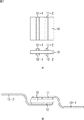
図1は、一般的なセルの構成例を示す図である。図1Aには、セル10の平面図および正面図が示されており、図1Bには、配線が接続された状態におけるセル10の側面図が示されている。
FIG. 1 is a diagram illustrating a configuration example of a general cell. FIG. 1A shows a plan view and a front view of the
図1に示すように、セル10は、2本のプラス電極11−1および11−2が表面に設けられ、2本のマイナス電極12−1および12−2が裏面に設けられている。なお、以下適宜、プラス電極11−1および11−2を区別する必要がない場合、プラス電極11と称し、マイナス電極12−1および12−2を区別する必要がない場合、マイナス電極12と称する。
As shown in FIG. 1, the
セル10のプラス電極11は、配線13−1を介して、他のセル10のマイナス電極12(図示せず)に接続され、セル10のマイナス電極12は、配線13−2を介して、他のセル10のプラス電極11(図示せず)に接続される。
The
一般的に、一つのセル10の起電力は0.5V程度であり、この電圧では商用電圧に変換することは困難である。そこで、太陽光発電モジュールは、複数のセル10が電気的に直列に接続された構成とすることにより、商用電圧に変換するのに効率の良い180〜360V程度まで高電圧化された電力を出力することができる。従って、このような高電圧を得ることができるように、通常、数百個のセル10が直列に接続されて太陽光発電モジュールが構成される。
In general, the electromotive force of one
ここで、数百個のセル10を直列に接続するということは、それらのセル10のうち一つでも不具合のあるセル10が発生すると、そのセル10において電流が遮断されてしまい、他のセル10により発電された電力を出力することが困難となる。そのため、従来、20〜100個のセル10が直列に接続されて構成される太陽光発電モジュールごとに、バイパスダイオードを設けることで、不具合の発生したセル10を有する太陽光発電モジュールがバイパスされるように構成される。
Here, connecting several hundred
図2は、従来の太陽光発電モジュールの構成例を示す図である。 FIG. 2 is a diagram illustrating a configuration example of a conventional photovoltaic power generation module.
図2に示されている太陽光発電モジュール21は、20個のセル10−1乃至10−20、およびバイパスダイオード22を備えて構成されている。
The photovoltaic
太陽光発電モジュール21では、セル10−1のプラス電極がバイパスダイオード22のカソードに接続され、セル10−1のマイナス電極がセル10−2のプラス電極に接続され、セル10−2のマイナス電極がセル10−3のプラス電極に接続される。そして、以下、同様に、セル10−20まで電気的に直列に接続され、セル10−20のマイナス電極がバイパスダイオード22のアノードに接続される。
In the photovoltaic
例えば、太陽光が雲や建造物などにより遮光され、太陽光発電モジュール21の一部分に影が発生すると、その陰の影響により、直列に接続されたセル10−1乃至10−20の出力が低下する。このとき、バイパスダイオード22により太陽光発電モジュール21がバイパスされ、その太陽光発電モジュール21の出力のみが低下し、太陽光発電装置全体として大きく出力が低下することを回避することができる。
For example, when sunlight is blocked by a cloud or a building and a shadow is generated in a part of the photovoltaic
また、例えば、特許文献1には、日照状態が悪くて発電していないセルをバイパスする手段として、MOS-FET(Metal Oxide Semiconductor Field Effect Transistor)を使用した太陽光発電モジュールが開示されている。
Further, for example,
上述したように、従来の太陽光発電装置は、太陽光発電モジュールごとにバイパスダイオードが設けられており、一部のセルに不具合が発生した場合には、そのセルを有する太陽光発電モジュール単位でバイパスされる。そのため、その太陽光発電モジュールにおいて不具合の発生していないセルで発電された電力も出力されないことになり、効率が悪かった。 As described above, in the conventional photovoltaic power generation apparatus, a bypass diode is provided for each photovoltaic power generation module. When a malfunction occurs in some cells, the photovoltaic power generation module unit having the cell is used. Bypassed. For this reason, the power generated in a cell in which no problem occurs in the solar power generation module is not output, and the efficiency is poor.
一般的に、太陽光発電モジュールを構成する複数のセルは密封された構造となっており、施工後に外部から不具合の発生したセルのみをバイパスさせて、太陽光発電モジュール全体として出力が低下することを回避することは困難であった。 Generally, a plurality of cells constituting a photovoltaic power generation module have a sealed structure, and after construction, by bypassing only cells that have malfunctioned from the outside, the output of the entire photovoltaic power generation module is reduced. It was difficult to avoid.
本発明は、このような状況に鑑みてなされたものであり、発電特性の低下をより効率的に抑制することができるようにするものである。 This invention is made | formed in view of such a condition, and makes it possible to suppress the fall of a power generation characteristic more efficiently.
本発明の一側面の太陽光発電モジュールは、受光した光に応じて発電し、直列に接続される複数のセルと、外部からの動作に応じて前記セルそれぞれをバイパスする複数のバイパス部とを備える。 A photovoltaic power generation module according to one aspect of the present invention generates power according to received light, and includes a plurality of cells connected in series and a plurality of bypass units that bypass each of the cells according to an operation from the outside. Prepare.
本発明の一側面の検査方法は、受光した光に応じて発電し、直列に接続される複数のセルと、外部からの動作に応じて前記セルそれぞれをバイパスする複数のバイパス部とを有する太陽光発電モジュールと、前記太陽光発電モジュールから出力される電力の電圧を測定する電圧測定部と、前記太陽光発電モジュールから出力される電力の電流を測定する電流測定部と、前記電圧および電流を監視し、前記バイパス部によるバイパスを制御する制御部とを備える太陽光発電モジュール自動検査システムの検査方法において、検査対象となる前記セルを順次選択し、選択された前記セルを、そのセルに対応する前記バイパス部によりバイパスさせ、前記電圧および電流に基づいてバイパスされた前記セルが正常であるか否かを判定し、正常でないと判定された前記セルを記録するステップを含む。 An inspection method according to an aspect of the present invention is a solar power generation system that generates power in response to received light and includes a plurality of cells connected in series and a plurality of bypass units that bypass the cells in response to external operations. A photovoltaic module, a voltage measuring unit that measures the voltage of power output from the photovoltaic module, a current measuring unit that measures the current of power output from the photovoltaic module, and the voltage and current In the inspection method of the photovoltaic power generation module automatic inspection system that includes a control unit that monitors and controls bypass by the bypass unit, the cells to be inspected are sequentially selected, and the selected cells correspond to the cells. To determine whether or not the bypassed cell is normal based on the voltage and current, and is not normal Comprising the step of recording the determined the cell.
本発明の一側面においては、受光した光に応じて発電し、直列に接続される複数のセルが、外部からの動作に応じてバイパスする複数のバイパス部によりそれぞれバイパスされる。 In one aspect of the present invention, a plurality of cells that generate electricity according to received light and are connected in series are bypassed by a plurality of bypass units that bypass according to an operation from the outside.
本発明の一側面によれば、発電特性の低下をより効率的に抑制することができる。 According to one aspect of the present invention, it is possible to more efficiently suppress a decrease in power generation characteristics.
以下、本発明を適用した具体的な実施の形態について、図面を参照しながら詳細に説明する。 Hereinafter, specific embodiments to which the present invention is applied will be described in detail with reference to the drawings.
図3は、本発明を適用した太陽光発電モジュールの第1の実施の形態の構成例を示す図である。 FIG. 3 is a diagram illustrating a configuration example of the first embodiment of the photovoltaic power generation module to which the present invention is applied.
図3に示すように、太陽光発電モジュール21Aは、20個のセル10−1乃至10−20が直列に接続され、その両端にバイパスダイオード22が接続されている点で、図2の太陽光発電モジュール21と同様に構成されている。但し、太陽光発電モジュール21Aは、セル10−1乃至10−20それぞれに対応するバイパススイッチ23−1乃至23−20を備える点で、図2の太陽光発電モジュール21と異なる構成となっている。
As shown in FIG. 3, the photovoltaic
即ち、太陽光発電モジュール21Aでは、バイパススイッチ23−1が、セル10−1のプラス電極とマイナス電極との間を開閉可能なように配置される。また、バイパススイッチ23−2が、セル10−2のプラス電極とマイナス電極との間を開閉可能なように配置されており、以下、同様に、バイパススイッチ23−20が、セル10−20のプラス電極とマイナス電極との間を開閉可能なように配置されている。
That is, in the photovoltaic
セル10−1乃至10−20およびバイパススイッチ23−1乃至23−20は、太陽光発電モジュール21Aの筐体の内部に封入されており、バイパススイッチ23−1乃至23−20は、その筐体の外部からの磁力によって接点が接続される構造となっている。例えば、太陽光発電モジュール21Aでは、バイパススイッチ23−1乃至23−20それぞれに外部から磁石を近接させる操作をユーザが行うことで、セル10−1乃至10−20のプラス電極とマイナス電極とが個別に短絡されるように構成されている。ここで、バイパススイッチ23−1乃至23−20のそれぞれ区別する必要がない場合、以下、適宜、バイパススイッチ23と称する。
The cells 10-1 to 10-20 and the bypass switches 23-1 to 23-20 are enclosed in the housing of the photovoltaic
このように、太陽光発電モジュール21Aは、いずれかのセル10に不具合が発生した場合、そのセル10に対応するバイパススイッチ23にユーザが外部から磁石を近接させることで、不具合が発生したセル10をバイパスさせることができる。これにより、不具合が発生したセル10を迂回して、他のセル10により発電された電力を太陽光発電モジュール21Aから出力することができ、太陽光発電モジュール21A全体の出力が低下することを回避することができる。即ち、太陽光発電モジュール21Aの発電特性の低下を抑制することができる。
As described above, when a failure occurs in any of the
次に、バイパススイッチ23の構成について説明する。
Next, the configuration of the
バイパススイッチ23としては、一般的な磁気近接スイッチを使用してもよいが、太陽光発電モジュール21Aの内部にバイパススイッチ23を配置することを考慮すると、バイパススイッチ23の高さは、可能な限りセル10と同程度にすることが望ましい。即ち、バイパススイッチ23の高さは数mm以内の低背タイプのものが望ましい。一方、バイパススイッチ23の面積に対しての自由度は大きいことから、近接される磁石に引き付けられる磁性体(鉄やニッケルなど)の接点は大きくすることができる。従って、磁性体を大きくすることで、バイパススイッチ23は、強力な磁石を使用することなく動作することができる。
As the
図4は、バイパススイッチ23の構成例を示す図である。図4Aには、開放状態のバイパススイッチ23が示されており、図4Bには、接続状態のバイパススイッチ23が示されている。
FIG. 4 is a diagram illustrating a configuration example of the
図4に示すように、バイパススイッチ23は、コイルばね31、固定接触部32−1および32−2、可動接触部33−1および33−2、並びに、磁性部材34を備えて構成される。
As shown in FIG. 4, the
また、バイパススイッチ23は、セル10を封入する筐体として太陽光発電モジュール21Aの背面側に配置されるバックシート41の内壁面に固定される。即ち、バックシート41に対して固定接触部32−1および32−2が固定されるとともに、コイルばね31の一端が、固定接触部32−1と32−2との間に固定される。また、コイルばね31の他端には磁性部材34が取り付けられており、磁性部材34の両端近傍には、可動接触部33−1および33−2が固定されている。そして、可動接触部33−1および33−2は、固定接触部32−1および32−2に向かい合うように磁性部材34の両端近傍に配置される。
Further, the
固定接触部32−1には、例えば、セル10のプラス端子に接続される配線42−1が電気的に接続されており、固定接触部32−2には、例えば、セル10のマイナス端子に接続される配線42−2が電気的に接続されている。磁性部材34は、鉄などの磁力に反応する材質で構成されるとともに、バックシート41は、樹脂やガラスなどの磁力を遮らない材質により構成される。
For example, a wiring 42-1 connected to the plus terminal of the
このようにバイパススイッチ23は構成されており、通常の状態(外部からの操作が行われない状態)では、図4Aに示すように、コイルばね31の付勢力によって固定接触部32−1および32−2と可動接触部33−1および33−2とが接触しない状態を維持しており、バイパススイッチ23は開放状態とされる。
In this way, the
そして、図4Bに示すように、太陽光発電モジュール21Aの外側から、バイパススイッチ23が配置されている箇所のバックシート41の外壁面に、ユーザが磁石43を近接させると、磁石43の磁力により磁性部材34が引き寄せられる。これにより、固定接触部32−1および32−2と可動接触部33−1および33−2とが接触する状態となって磁性部材34を介して電流を流すことが可能となり、バイパススイッチ23は接続状態とされる。
As shown in FIG. 4B, when the user brings the
このように磁石43を近接させてバイパススイッチ23を接続状態とすることにより、セル10のプラス端子とマイナス端子とを短絡することができる。これにより、例えば、不具合が発生したセル10に対応するバイパススイッチ23を接続状態とすることで、そのセル10をバイパスして、太陽光発電モジュール21A全体から出力が行われなくなることを回避することができる。
Thus, the plus terminal and minus terminal of the
即ち、太陽光発電モジュール21Aでは、バイパススイッチ23が筐体に封入された状態で施工された後であっても、外部からバイパススイッチ23に対する操作を行うことができ、不具合が発生したセル10をバイパスすることができ、そのメンテナンスを行うことができる。即ち、通常、太陽光発電モジュールは、樹脂などで含浸処理されるため、完成後はセル単位での補充は困難であり太陽光発電モジュール全体を交換する必要があったのに対し、太陽光発電モジュール21Aでは、セル10ごとにメンテナンスを行うことで全体を交換することが回避される。従って、太陽光発電モジュール21Aを建材用に使用した場合でも、施工後に不具合が発生した場合のリスクを最小限に軽減することができる。
That is, in the solar
また、バイパススイッチ23では、付勢手段としてコイルばね31のような単純な部品を採用することにより、シンプルな構造かつ低コストで構成することができる。なお、付勢手段として、コイルばね31以外の部品を採用してもよい。
Further, the
即ち、図5には、バイパススイッチ23の変形例が示されている。図5Aには、開放状態のバイパススイッチ23’が示されており、図5Bには、接続状態のバイパススイッチ23’が示されている。
That is, FIG. 5 shows a modified example of the
図5に示すように、バイパススイッチ23’は、板ばね35、固定接触部32’、可動接触部33’、および磁性部材34’を備えて構成される。即ち、バイパススイッチ23’では、図4のバイパススイッチ23のコイルばね31に替えて、板ばね35が使用される。
As shown in FIG. 5, the
固定接触部32’には、例えば、セル10のプラス端子に接続される配線42−1が電気的に接続されており、板ばね35の一端には、例えば、セル10のマイナス端子に接続される配線42−2が電気的に接続されている。また、板ばね35の他端には、可動接触部33’および磁性部材34’が取り付けられている。
For example, a wiring 42-1 connected to the plus terminal of the
バイパススイッチ23’では、通常の状態では、図5Aに示すように、板ばね35の付勢力によって固定接触部32’と可動接触部33’とが接触しない状態が維持され、バイパススイッチ23’は開放状態とされる。そして、図5Bに示すように、ユーザが磁石43を近接させると、磁石43の磁力により磁性部材34’が引き寄せられ、固定接触部32’と可動接触部33’とが接触する状態となって板ばね35を介して電流を流すことが可能となり、バイパススイッチ23’が接続状態とされる。
In the normal state, as shown in FIG. 5A, the
なお、図4および図5では、太陽光発電モジュール21Aの背面側からバックシート41を介してバイパススイッチ23および23’に対する操作を行うような構成となっているが、太陽光発電モジュール21Aの表面からバイパススイッチ23に対する操作を行うような構成とすることができる。
4 and 5, the operation is performed on the bypass switches 23 and 23 ′ from the back side of the solar
ここで、図3に示した太陽光発電モジュール21Aのように、太陽光発電モジュール21Aを構成する全てのセル10−1乃至10−20に対してバイパススイッチ23−1乃至23−20が備えられる構成が理想的である。しかしながら、内部の配線が煩雑になることや、製作コストの低減、製作時における作業性の向上などの観点から、太陽光発電モジュール21Aの構成を簡略化することが望ましい。
Here, like the photovoltaic
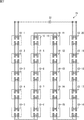
次に、図6は、太陽光発電モジュールの第2の実施の形態の構成例を示す図である。 Next, FIG. 6 is a diagram illustrating a configuration example of the second embodiment of the solar power generation module.
図6に示されている太陽光発電モジュール21Bは、20個のセル10’−1乃至10’−20が直列に接続され、その両端にバイパスダイオード22が接続されており、16個のバイパススイッチ23−1乃至23−16を備えて構成される。また、太陽光発電モジュール21Bで使用されているセル10’は、一方の側面近傍にプラス電極が配置され、他方の側面近傍にマイナス電極が配置されるように構成されている。
A photovoltaic
太陽光発電モジュール21Bでは、セル10’−1のマイナス電極とセル10’−2のプラス電極とが接続される一方、セル10’−1のプラス電極とセル10’−2のマイナス電極との間にバイパススイッチ23−1が配置される。また、セル10’−2のマイナス電極とセル10’−3のプラス電極とが接続される一方、セル10’−2のプラス電極とセル10’−3のマイナス電極との間にバイパススイッチ23−2が配置される。以下、同様に、太陽光発電モジュール21Bでは、セル10’のプラス電極と、隣接するセル10’のマイナス電極との接続において、交互にバイパススイッチ23が配置される。
In the photovoltaic
このように太陽光発電モジュール21Bは構成されており、いずれかのセル10’に不具合が発生した場合、そのセル10’の両側のいずれか一方のバイパススイッチ23を接続状態とすることで、不具合の発生したセル10’をバイパスすることができる。その際、不具合の発生したセル10’に隣接する、接続状態としたバイパススイッチ23側のセル10’もバイパスされる。即ち、太陽光発電モジュール21Bでは、2つのセル10’単位でバイパスされる。なお、不具合の発生したセル10’に対してどちら側のバイパススイッチ23を接続状態とするかは、任意に選択することができる。
As described above, the photovoltaic
このように、太陽光発電モジュール21Bでは、2つのセル10’単位でバイパス可能なようにバイパススイッチ23が配置されて構成される。これにより、太陽光発電モジュール21Bでは、太陽光発電モジュール21Aよりも、配線をシンプルに構成することができるとともに、バイパススイッチ23の個数を20個から16個に削減することができる。
Thus, in the photovoltaic
次に、図7は、太陽光発電モジュールの第3の実施の形態の構成例を示す図である。 Next, FIG. 7 is a diagram illustrating a configuration example of the third embodiment of the photovoltaic power generation module.
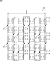
図7に示されている太陽光発電モジュール21Cは、20個のセル10’−1乃至10’−20が直列に接続され、その両端にバイパスダイオード22が接続されている点で、図6の太陽光発電モジュール21Bと同様に構成されている。但し、太陽光発電モジュール21Cは、10個のバイパススイッチ23−1乃至23−10を備えており、バイパススイッチ23−1乃至23−10の接続構成が図6の太陽光発電モジュール21Bと異なっている。
The solar power generation module 21C shown in FIG. 7 includes 20
即ち、太陽光発電モジュール21Cでは、セル10’−1のマイナス電極とセル10’−2のプラス電極とが接続される一方、セル10’−1のプラス電極とセル10’−2のマイナス電極との間にバイパススイッチ23−1が配置される。また、セル10’−2のマイナス電極とセル10’−3のプラス電極とが接続される。ここで、セル10’−2のプラス電極とセル10’−3のマイナス電極とは接続されない。
That is, in the solar power generation module 21C, the minus electrode of the
そして、太陽光発電モジュール21Cでは、セル10’−3のマイナス電極とセル10’−4のプラス電極とが接続される一方、セル10’−3のプラス電極とセル10’−4のマイナス電極との間にバイパススイッチ23−2が配置される。以下、同様に、太陽光発電モジュール21Cでは、隣り合う一組のセル10’ごとにバイパススイッチ23が配置される。
In the solar power generation module 21C, the minus electrode of the
このように太陽光発電モジュール21Cは構成されており、いずれかのセル10’に不具合が発生した場合、そのセル10’と隣接するセル10’との間のバイパススイッチ23を接続状態とすることで、不具合の発生したセル10’をバイパスすることができる。その際、不具合の発生したセル10’に隣接するセル10’もバイパスされる。即ち、太陽光発電モジュール21Cは、バイパスされるセル10’の組み合わせが重複することなく、あるセル10’に不具合が発生した場合、そのセル10’とともにバイパスされるセル10’が予め決められた構成となっている。
In this way, the photovoltaic power generation module 21C is configured, and when a failure occurs in any of the
このように、太陽光発電モジュール21Cでは、2つのセル10’単位でバイパス可能なようにバイパススイッチ23が配置されて構成される。これにより、太陽光発電モジュール21Cでは、太陽光発電モジュール21Aよりも、配線をシンプルに構成することができるとともに、バイパススイッチ23の個数を20個から10個に削減することができる。なお、バイパスするセル10’の設定は、1個ごとまたは複数個(2個以上でも可)ごとなど自由に設計可能であり、用途やコストに応じて使い分けることができる。
Thus, in the photovoltaic power generation module 21C, the
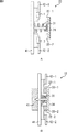
次に、図8を参照して、太陽光発電モジュール21Aを実際に使用する場合において、メンテナンスを実施する例について説明する。図8Aには、太陽光発電モジュール21Aの表面が示されており、図8Bには、太陽光発電モジュール21Aの裏面が示されている。
Next, an example in which maintenance is performed when the solar
太陽光発電モジュール21Aの表面は、ガラスやアクリル樹脂などの透明な板材からなるフロントシート44により覆われ、太陽光発電モジュール21Aの裏面は、図4および図5を参照して説明したようなバックシート41により覆われている。また、太陽光発電モジュール21Aの側面は、図示しない部材により囲われており、セル10−1乃至10−20は太陽光発電モジュール21Aの筐体内部に封入されている。
The surface of the solar
また、太陽光発電モジュール21Aは、図3に示したように、セル10−1乃至10−20それぞれに対応するバイパススイッチ23−1乃至23−20を備えている。そして、バックシート41には、太陽光発電モジュール21Aの内部に配置されているバイパススイッチ23−1乃至23−20に対応する箇所に、マーキング24−1乃至24−20が標記されている。
Moreover, the solar
例えば、ユーザは、検査しようとする太陽光発電モジュール21Aの出力電圧および出力電流をモニタしながら、マーキング24−1乃至24−20に対して永久磁石を順次近接させる。そして、正常なセル10に対応するバイパススイッチ23のマーキング24に対して永久磁石を近接させ、そのセル10をバイパスさせる操作をした場合、そのセル10により発電されている電力量に応じて、太陽光発電モジュール21Aの出力電圧および出力電流が減少する。これに対し、不具合が発生したセル10に対応するバイパススイッチ23のマーキング24に対して永久磁石を近接させ、そのセル10をバイパスさせる操作をした場合、不具合が発生したセル10による電流の遮断が回避され、太陽光発電モジュール21Aの出力電流が増加する。
For example, the user sequentially brings the permanent magnets close to the markings 24-1 to 24-20 while monitoring the output voltage and output current of the photovoltaic
このように出力電流が増加することにより、ユーザは、セル10の出力電流が増加したときに操作の対象となったセル10に不具合が発生していることを容易に検知することができる。
As the output current increases in this way, the user can easily detect that a defect has occurred in the
従って、太陽光発電モジュール21Aに対する検査によって不具合が発生したセル10を検知した場合、ユーザは、例えば、そのセル10に対応するマーキング24の箇所に永久磁石を接着剤などで固定する処理を施すことができる。これにより、不具合が発生したセル10に対応するバイパススイッチ23によりそのセル10を常にバイパスすることができ、太陽光発電モジュール21Aの全体として特性が低下することを回避することができる。即ち、太陽光発電モジュール21Aは、不具合の発生したセル10のみを最小限に迂回して、他のセル10からの出力を維持することができる。このように、用意かつ確実にメンテナンスを実施することができる。
Therefore, when a
また、太陽光発電モジュール21Aの外部環境の変化により、例えば、設置場所の近隣に建造物が新たに建設されたことによって日照条件が変化することにより、太陽光発電モジュール21Aの一部のセル10に恒久的に太陽光が照射されなくなる場合がある。このような場合でも、ユーザは、恒久的に太陽光が照射されないセル10に対応するバイパススイッチ23により、そのセル10がバイパスされるように外部から操作をすることができる。これにより、太陽光発電モジュール21A全体として発電特性が低下することを抑制することができる。
Further, due to a change in the external environment of the solar
なお、例えば、バックシート41が、透明な樹脂やガラスにより構成されていて、太陽光発電モジュール21Aの内部に配置されているバイパススイッチ23−1乃至23−20を、外部から視認することができる場合、マーキング24−1乃至24−20の標記は不要である。
For example, the
なお、図3の太陽光発電モジュール21Aは、外部から磁石を近接させるとバイパススイッチ23−1乃至23−20が接続状態となるように構成されているが、バイパススイッチ23−1乃至23−20の開放と接続との切り替えを磁気コイルにより行ってもよい。例えば、マーキング24−1乃至24−20で標記されているように、太陽光発電モジュール21Aでは、バイパススイッチ23−1乃至23−20が配置される位置は決まっている。そこで、それぞれ対応する箇所に磁気コイルを配設して、それらの磁気コイルによりバイパススイッチ23−1乃至23−20を電気的に駆動させることができる。
In addition, although the solar
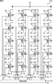
図9には、バイパススイッチ23−1乃至23−20を駆動する駆動回路の配線図が示されている。 FIG. 9 shows a wiring diagram of a drive circuit for driving the bypass switches 23-1 to 23-20.
図9に示すように、駆動回路51は、20個の磁気コイル52−1乃至52−20、および4つの制御スイッチ53−1乃至53−4を備えて構成される。
As shown in FIG. 9, the
磁気コイル52−1乃至52−20は、太陽光発電モジュール21Aの内部に配置されているバイパススイッチ23−1乃至23−20に対応する箇所(例えば、図8のマーキング24−1乃至24−20の箇所)に配設される。
The magnetic coils 52-1 to 52-20 correspond to locations corresponding to the bypass switches 23-1 to 23-20 disposed inside the solar
また、磁気コイル52−1乃至52−20の一端は、電源VLに接続されているとともに、それらの他端は、制御スイッチ53−1乃至53−4を介して接地されている。即ち、磁気コイル52−1乃至52−5の他端は、制御スイッチ53−1を介して接地され、磁気コイル52−6乃至52−10の他端は、制御スイッチ53−2を介して接地され、磁気コイル52−11乃至52−15の他端は、制御スイッチ53−3を介して接地され、磁気コイル52−16乃至52−20の他端は、制御スイッチ53−4を介して接地されている。 One end of each of the magnetic coils 52-1 to 52-20 is connected to the power source VL, and the other end thereof is grounded via the control switches 53-1 to 53-4. That is, the other ends of the magnetic coils 52-1 to 52-5 are grounded via the control switch 53-1, and the other ends of the magnetic coils 52-6 to 52-10 are grounded via the control switch 53-2. The other ends of the magnetic coils 52-11 to 52-15 are grounded via the control switch 53-3, and the other ends of the magnetic coils 52-16 to 52-20 are grounded via the control switch 53-4. Has been.
例えば、ユーザは、制御スイッチ53−1乃至53−4を操作することで、磁気コイル52−1乃至52−20それぞれを個別に選択して接地させ、その選択された磁気コイル52に電流を流すことができる。これにより、選択された磁気コイル52に電磁力が発生し、その磁気コイル52の配設箇所にあるバイパススイッチ23が閉鎖状態となって、閉鎖状態のバイパススイッチ23に対応するセル10をバイパスすることができる。
For example, the user operates the control switches 53-1 to 53-4 to individually select and ground each of the magnetic coils 52-1 to 52-20, and to supply a current to the selected magnetic coil 52. be able to. As a result, an electromagnetic force is generated in the selected magnetic coil 52, and the
このように、駆動回路51を利用することにより、ユーザは、任意のバイパススイッチ23を自由に選択して開閉することができる。従って、上述したように磁石を近接させるような検査方法よりも、より容易に太陽光発電モジュール21Aを検査することができる。
In this way, by using the
なお、磁気コイル52−1乃至52−20は、予め太陽光発電モジュール21Aの背面に固定しておくことができる他、必要に応じて取り外しができるような構造とすることができる。また、太陽光発電モジュール21Aを検査する際にのみ磁気コイル52−1乃至52−20を取り付けることが好ましい。この場合、例えば、磁気コイル52−1乃至52−20の配置を固定するフレームなどに磁気コイル52−1乃至52−20を取り付け、そのフレームごと太陽光発電モジュール21Aの背面に磁気コイル52−1乃至52−20を配設するような構成を採用することができる。
In addition, the magnetic coils 52-1 to 52-20 can be fixed to the back surface of the photovoltaic
また、セル10をバイパスするバイパス手段としては、バイパススイッチ23のようなスイッチを使用する他、例えば、FET(Field Effect Transistor:電界効果トランジスタ)を使用することができる。
Further, as a bypass means for bypassing the
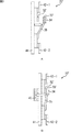
次に、図10は、本発明を適用した太陽光発電モジュールの第4の実施の形態の構成例を示す図である。図10には、太陽光発電モジュール21Dの配線図が示されている。 Next, FIG. 10 is a figure which shows the structural example of 4th Embodiment of the solar power generation module to which this invention is applied. FIG. 10 shows a wiring diagram of the solar power generation module 21D.
図10に示されている太陽光発電モジュール21Dは、20個のセル10−1乃至10−20およびバイパスダイオード22を備える点で、図3の太陽光発電モジュール21Aと同様に構成される。
A photovoltaic power generation module 21D shown in FIG. 10 is configured in the same manner as the photovoltaic
一方、太陽光発電モジュール21Dは、20個のFET61−1乃至61−20、4つの入出力ポート(I/O)62−1乃至62−4、および絶縁回路63を備える点で、太陽光発電モジュール21Aと異なる構成となっている。即ち、太陽光発電モジュール21Dでは、太陽光発電モジュール21Aのバイパススイッチ23−1乃至23−20に替えて、FET61−1乃至61−20がセル10−1乃至10−20それぞれに対応して設けられている。
On the other hand, the photovoltaic power generation module 21D is a photovoltaic power generation in that it includes 20 FETs 61-1 to 61-20, four input / output ports (I / O) 62-1 to 62-4, and an insulating
FET61−1乃至61−20のソースは、それぞれ対応するセル10−1乃至10−20のプラス電極に接続され、FET61−1乃至61−20のドレインは、それぞれ対応するセル10−1乃至10−20のマイナス電極に接続される。また、FET61−1乃至61−5のゲートは、入出力ポート62−1を介して、絶縁回路63に接続され、FET61−6乃至61−10のゲートは、入出力ポート62−2を介して、絶縁回路63に接続される。また、FET61−11乃至61−15のゲートは、入出力ポート62−3を介して、絶縁回路63に接続され、FET61−16乃至61−20のゲートは、入出力ポート62−4を介して、絶縁回路63に接続される。
The sources of the FETs 61-1 to 61-20 are connected to the positive electrodes of the corresponding cells 10-1 to 10-20, respectively, and the drains of the FETs 61-1 to 61-20 are respectively connected to the corresponding cells 10-1 to 10-20. Connected to 20 negative electrodes. The gates of the FETs 61-1 to 61-5 are connected to the insulating
絶縁回路63には、例えば、FET61−1乃至61−20のいずれかを選択することを示すスイッチ選択シリアルデータが供給される。絶縁回路63は、スイッチ選択シリアルデータに従い、それぞれ対応する入出力ポート62−1乃至62−4を介して、FET61−1乃至61−20を個別に絶縁する。これにより、スイッチ選択シリアルデータで選択されたFET61に対応するセル10がバイパスされる。
For example, switch selection serial data indicating that any one of the FETs 61-1 to 61-20 is selected is supplied to the insulating
このように、太陽光発電モジュール21Dでは、セル10−1乃至10−20のバイパス手段として、FET61−1乃至61−20を採用することにより、機械的な接点を有するスイッチと比較して、酸化や腐食などの心配がないことから、長期間の保存または使用に優れている。また、FET61−1乃至61−20は、ON抵抗やバラツキが少ない点でも優れている。 As described above, in the photovoltaic power generation module 21D, by adopting the FETs 61-1 to 61-20 as the bypass means of the cells 10-1 to 10-20, it is oxidized compared to the switch having mechanical contacts. It is excellent for long-term storage or use because there is no worry about corrosion or corrosion. Further, the FETs 61-1 to 61-20 are excellent in that they have less ON resistance and variation.
また、太陽光発電モジュール21Dでは、FET61−1乃至61−20のためのゲート線を内部に配線したり電源ラインが必要となるが、それらの配線が煩雑とならないように、太陽光発電モジュール21Dは、太陽光発電モジュール21Dの出力を基準電源とし、FET61−1乃至61−20のゲートを制御側で絶縁して動作するように構成されている。 Further, in the photovoltaic power generation module 21D, gate lines for the FETs 61-1 to 61-20 are required and power supply lines are required, but the photovoltaic power generation module 21D is not required to make the wiring complicated. Is configured to operate with the output of the photovoltaic power generation module 21D as a reference power source and the gates of the FETs 61-1 to 61-20 insulated on the control side.
なお、スイッチ選択シリアルデータは、例えば、ユーザが太陽光発電モジュール21Dの出力を検査する際に、所定の検査機器を操作することにより絶縁回路63に供給される。または、太陽光発電モジュール21Dの出力電圧および出力電流を監視しながら、FET61−1乃至61−20を順次切り替えて自動的に検査を行う制御手段を設け、その制御手段からスイッチ選択シリアルデータが絶縁回路63に供給されるようにしてもよい。
The switch selection serial data is supplied to the insulating
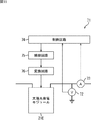
次に、図11は、太陽光発電モジュールの自動検査システムの構成例を示すブロック図である。 Next, FIG. 11 is a block diagram illustrating a configuration example of an automatic inspection system for a photovoltaic power generation module.
図11に示すように、自動検査システム71は、太陽光発電モジュール21E、電圧測定部72、電流測定部73、制御回路74、絶縁回路75、および変換回路76を備えて構成される。
As shown in FIG. 11, the
太陽光発電モジュール21Eは、例えば、図10に示す太陽光発電モジュール21Dと同様に、20個のセル10−1乃至10−20、バイパスダイオード22、および20個のFET61−1乃至61−20を備えて構成されている。即ち、太陽光発電モジュール21Eでは、セル10−1乃至10−20が電気的に直列に接続され、セル10−1とセル10−20との間にバイパスダイオード22が接続され、セル10−1乃至10−20ごとにFET61−1乃至61−20が設けられている。
The solar
電圧測定部72は、太陽光発電モジュール21Eから出力される電力の電圧(グランドレベルとの電位差)を測定しており、所定のタイミングで、制御回路74により電圧値がサンプリングされる。電流測定部73は、太陽光発電モジュール21Eから出力される電力の電流を測定しており、所定のタイミングで、制御回路74により電流値がサンプリングされる。
The
制御回路74は、電圧測定部72により測定された電圧値、および電流測定部73により測定された電流値を監視し、太陽光発電モジュール21Eが備えるFET61−1乃至61−20を順次選択するスイッチ選択シリアルデータを絶縁回路75に共有する。
The
絶縁回路75は、制御回路74からのスイッチ選択シリアルデータに従って、変換回路76を介して、FET61−1乃至61−20を順次絶縁する。絶縁回路75からFET61−1乃至61−20を絶縁するために出力される信号はシリアル信号であり、変換回路76は、その信号をパラレル信号に変換する。
The
上述したように、不具合が発生したセル10に対応するFET61を絶縁した場合、そのセル10がバイパスされるため、太陽光発電モジュール21Eから出力される電力の電流が増加する。従って、自動検査システム71では、制御回路74が電圧値および電流値をモニタリングしながら、FET61−1乃至61−20を順次絶縁することで、不具合が発生したセル10を検出することができる。
As described above, when the
なお、図11の自動検査システム71では、セル10をバイパスするバイパス手段としてFET61を使用した例について説明したが、例えば、図3を参照して説明したようなバイパススイッチ23をバイパス手段として使用し、図9を参照して説明したような磁気コイル52を制御回路74により制御することで、バイパススイッチ23の開閉を制御してもよい。
In the
次に、図12は、図11の自動検査システム71において太陽光発電モジュール21Eを検査する処理を説明するフローチャートである。
Next, FIG. 12 is a flowchart for explaining processing for inspecting the photovoltaic
ステップS11において、制御回路74は、検査を行う初期設定として、検査対象となるセル10のアドレスを指定する変数nに1をセットし、初期段階(セル10をバイパスしない状態)での電圧値および電流値をサンプリングして、処理はステップS12に進む。
In step S11, the
ステップS12において、制御回路74は、アドレスnのセル10―nが選択されたことを示すスイッチ選択シリアルデータを絶縁回路75に供給する。絶縁回路75は、スイッチ選択シリアルデータに従って変換回路76を介してFET61―nを絶縁し、これによりFET61―nがONになる。ステップS12の処理後、処理はステップS13に進む。
In step S12, the
ステップS13において、制御回路74は、電圧測定部72により測定されている電圧値をサンプリングし、処理はステップS14に進み、制御回路74は、電流測定部73により測定されている電流値をサンプリングする。
In step S13, the
ステップS14の処理後、処理はステップS15に進み、制御回路74は、アドレスnのセル10−nが正常であるか否かを判定する。例えば、制御回路74は、FET61―nをONにすることにより、太陽光発電モジュール21Eの出力電圧および出力電流が1つのセル10分だけ低下すると、セル10−nは正常であると判定する。一方、制御回路74は、FET61―nをONにすることにより、太陽光発電モジュール21Eの出力電流が増加すると、セル10−nは正常でない(異常が発生した)と判定する。
After the process of step S14, the process proceeds to step S15, and the
ステップS15において、制御回路74が、アドレスnのセル10−nが正常であると判定した場合、処理はステップS16をスキップしてステップS17に進む。
If the
一方、ステップS15において、制御回路74が、アドレスnのセル10−nが正常でないと判定した場合、処理はステップS16に進む。ステップS16において、制御回路74は、例えば内蔵する記録領域に、正常でないと判定したセル10のアドレス、即ち、現在のアドレスnを記録し、処理はステップS17に進む。
On the other hand, if the
ステップS17において、制御回路74は、全てのセル10に対する検査を行ったか否かを判定する。例えば、制御回路74は、太陽光発電モジュール21Eが備えるセル10の個数がNである場合、現在の変数nがN以上である場合、全てのセル10に対する検査を行ったと判定し、現在の変数nがN未満である場合、全てのセル10に対する検査を行っていないと判定する。
In step S17, the
ステップS17において、制御回路74が、全てのセル10に対する検査を行っていないと判定した場合、処理はステップS18に進み、制御回路74は、変数nをインクリメント(n=n+1)し、処理はステップS12に戻り、以下、同様の処理が繰り返される。
If the
一方、ステップS17において、制御回路74が、全てのセル10に対する検査を行ったと判定した場合、処理は終了される。
On the other hand, if the
以上のように、制御回路74は、太陽光発電モジュール21Eが備える全てのセル10を順次バイパスして、それぞれのセル10が正常であるか否かを判定し、正常でないと判定された、即ち、異常が発生したセル10を検出することができる。
As described above, the
制御回路74には、このような検査を行うプログラムが記録されており、一連の処理を自動的に行うことができ、制御回路74は、定期的に太陽光発電モジュール21Eを検査することができる。また、セル10の応答速度を考慮しても、1つのセル10あたり1秒以内で検査することができ、例えば、50個のセル10で構成される太陽光発電モジュール1枚の検査に要する時間は1分以内とすることができる。従って、太陽光発電モジュールの検査を毎日実施したとしても、一日の発電量に大きな影響を及ぼすことはない。
A program for performing such an inspection is recorded in the
また、このような検査を、一日のうちに数回行うことにより、例えば、時間帯によって日照が遮られることにより、不良となるセル10を検出することができる。また、このような検査を、一年を通して行うことにより、季節によって日照が遮られることにより、不良となるセル10を検出することができる。このように、制御回路74には、時間帯や季節などの外部環境によって不良となるセル10の情報が蓄積され、その履歴を参照することで、セル10が不良となる時間帯や季節などにおいて、そのセル10をバイパスするように設定することで、太陽光発電モジュール21Eを最適に制御することができる。
In addition, by performing such an inspection several times a day, for example, a
次に、図13は、図11の自動検査システム71において太陽光発電モジュール21Eを最適に制御するための設定を行う処理を説明するフローチャートである。
Next, FIG. 13 is a flowchart for explaining processing for performing settings for optimal control of the photovoltaic
ステップS21において、制御回路74は、設定を行う初期設定として、設定対象となるセル10のアドレスを指定する変数nに1をセットし、処理はステップS22に進む。
In step S21, the
ステップS22において、制御回路74は、内蔵する記憶領域に記憶されているアドレスnのセル10−nの履歴を参照する。
In step S22, the
ステップS22の処理後、処理はステップS23に進み、制御回路74は、ステップS22で参照した履歴に基づいて、アドレスnのセル10−nは、常に不良であるか否かを判定する。
After the process of step S22, the process proceeds to step S23, and the
ステップS23において、アドレスnのセル10−nは常に不良であると判定された場合、処理はステップS24に進み、制御回路74は、アドレスnのセル10−nは常にバイパスすると設定する。
If it is determined in step S23 that the cell 10-n at address n is always defective, the process proceeds to step S24, and the
一方、ステップS23において、アドレスnのセル10−nは、常に不良でないと判定された場合、処理はステップS25に進み、制御回路74は、ステップS22で参照した履歴に基づいて、セル10−nは外部環境によって不良となるか否かを判定する。
On the other hand, if it is determined in step S23 that the cell 10-n at the address n is not always defective, the process proceeds to step S25, and the
ステップS25において、アドレスnのセル10−nは外部環境によって不良となると判定された場合、処理はステップS26に進み、制御回路74は、ステップS22で参照した履歴に基づいて、アドレスnのセル10−nをバイパスするタイミングを設定する。即ち、セル10−nが不良となる時間帯および季節によりをセル10−nをバイパスするように設定する。
If it is determined in step S25 that the cell 10-n at the address n is defective due to the external environment, the process proceeds to step S26, and the
ステップS24またはS26の処理後、あるいは、ステップS25においてアドレスnのセル10−nは外部環境によって不良とならない(常に正常である)と判定された場合、処理はステップS27に進む。 After the process of step S24 or S26, or when it is determined in step S25 that the cell 10-n at the address n is not defective due to the external environment (always normal), the process proceeds to step S27.
ステップS27において、制御回路74は、全てのセル10に対する設定を行ったか否かを判定し、全てのセル10に対する設定を行っていないと判定した場合、処理はステップS28に進む。ステップS28において、制御回路74は、変数nをインクリメント(n=n+1)し、処理はステップS22に戻り、以下、同様の処理が繰り返される。
In step S27, the
一方、ステップS27において、制御回路74が、全てのセル10に対する設定を行ったと判定した場合、処理は終了される。
On the other hand, when the
以上のように、制御回路74は、不具合が発生したセル10に対しては常にバイパスすると設定することができるとともに、外部環境によって不良となるセル10に対しては、そのセル10をバイパスするタイミング(時間帯および季節)を設定することができる。これにより、例えば、セル10が不良となる条件が整った場合に、FET61を積極的にONにすることにより、太陽光発電モジュール21Eの発電量が減少することを効率よく回避することができる。
As described above, the
また、太陽光発電モジュール21Eを最適に制御するための設定を行う処理を所定の間隔で行うことにより、外部環境の変化により、例えば、設置場所の近隣に建造物が新たに建設されたことによって日照条件が変化することにより、不良となるセル10が新たに発生したとしても、そのセル10が適切にバイパスされるように設定することができ、太陽光発電モジュール21Eの発電特性の低下を適切に抑制することができる。
In addition, by performing processing for performing settings for optimal control of the solar
なお、太陽光発電装置が複数の太陽光発電モジュール21を備えて構成される場合、図12および図13を参照して説明した処理は、太陽光発電モジュール21ごとに行うことができ、制御回路74には、太陽光発電モジュール21ごとの履歴が記録される。即ち、制御回路74は、太陽光発電モジュール21ごとに最適な制御を行うことができる。
In addition, when a solar power generation device is provided with the some solar
なお、上述のフローチャートを参照して説明した各処理は、必ずしもフローチャートとして記載された順序に沿って時系列に処理する必要はなく、並列的あるいは個別に実行される処理(例えば、並列処理あるいはオブジェクトによる処理)も含むものである。また、プログラムは、1のCPUにより処理されるものであっても良いし、複数のCPUによって分散処理されるものであっても良い。 Note that the processes described with reference to the flowcharts described above do not necessarily have to be processed in chronological order in the order described in the flowcharts, but are performed in parallel or individually (for example, parallel processes or objects Processing). The program may be processed by one CPU, or may be distributedly processed by a plurality of CPUs.
また、本明細書において、システムとは、複数の装置により構成される装置全体を表すものである。 Further, in this specification, the system represents the entire apparatus constituted by a plurality of apparatuses.
なお、上述した一連の処理は、ハードウエアにより実行することもできるし、ソフトウエアにより実行することもできる。一連の処理をソフトウエアにより実行する場合には、そのソフトウエアを構成するプログラムが、専用のハードウエアに組み込まれているコンピュータ、または、各種のプログラムをインストールすることで、各種の機能を実行することが可能な、例えば汎用のコンピュータなどに、プログラム記録媒体からインストールされる。 The series of processes described above can be executed by hardware or can be executed by software. When a series of processing is executed by software, a program constituting the software executes various functions by installing a computer incorporated in dedicated hardware or various programs. For example, the program is installed in a general-purpose computer from a program recording medium.
コンピュータでは、ROM(Read Only Memory)に記憶されているプログラムや、ハードディスクや不揮発性のメモリなどよりなる記憶部に記憶されているプログラムなどが、RAM(Random Access Memory)にロードされ、CPU(Central Processing Unit)により実行される。それにより、上述した一連の処理が行われる。 In a computer, programs stored in ROM (Read Only Memory) or programs stored in a storage unit such as a hard disk or non-volatile memory are loaded into RAM (Random Access Memory) and CPU (Central Executed by the Processing Unit). Thereby, the series of processes described above are performed.
また、それらのプログラムは、あらかじめ記憶部に記憶させておく他、ネットワークインタフェースなどよりなる通信部を介して、あるいは、磁気ディスク(フレキシブルディスクを含む)、光ディスク(CD-ROM(Compact Disc-Read Only Memory),DVD(Digital Versatile Disc)等)、光磁気ディスク、または半導体メモリなどのリムーバブルメディアを駆動するドライブを介して、コンピュータにインストールすることができる。 These programs are stored in advance in a storage unit, or via a communication unit such as a network interface, or a magnetic disk (including a flexible disk), an optical disk (CD-ROM (Compact Disc-Read Only). Memory, DVD (Digital Versatile Disc, etc.), magneto-optical disk, or drive that drives removable media such as semiconductor memory can be installed in the computer.
なお、コンピュータが実行するプログラムは、本明細書で説明する順序に沿って時系列に処理が行われるプログラムであっても良いし、並列に、あるいは呼び出しが行われたとき等の必要なタイミングで処理が行われるプログラムであっても良い。また、プログラムは、1つのCPUにより処理されるものであっても良いし、複数のCPUによって分散処理されるものであっても良い。 The program executed by the computer may be a program that is processed in time series in the order described in this specification, or in parallel or at a necessary timing such as when a call is made. It may be a program for processing. Further, the program may be processed by a single CPU, or may be processed in a distributed manner by a plurality of CPUs.
なお、本発明の実施の形態は、上述した実施の形態に限定されるものではなく、本発明の要旨を逸脱しない範囲において種々の変更が可能である。 The embodiment of the present invention is not limited to the above-described embodiment, and various modifications can be made without departing from the gist of the present invention.
10 セル, 21 太陽光発電モジュール, 22 バイパスダイオード, 23 バイパススイッチ, 24 マーキング, 31 コイルばね, 32 固定接触部, 33 可動接触部, 34 磁性部材, 35 板ばね, 41 バックシート, 42 配線, 43 磁石, 44 フロントシート, 51 駆動回路, 52 磁気コイル, 53 制御スイッチ, 61 FET, 62 入出力ポート, 63 絶縁回路, 71 自動検査システム, 72 電圧測定部, 73 電流測定部, 74 制御回路, 75 絶縁回路, 76 変換回路 10 cells, 21 photovoltaic modules, 22 bypass diodes, 23 bypass switches, 24 markings, 31 coil springs, 32 fixed contact portions, 33 movable contact portions, 34 magnetic members, 35 leaf springs, 41 back sheets, 42 wirings, 43 Magnet, 44 Front seat, 51 Drive circuit, 52 Magnetic coil, 53 Control switch, 61 FET, 62 Input / output port, 63 Insulation circuit, 71 Automatic inspection system, 72 Voltage measurement unit, 73 Current measurement unit, 74 Control circuit, 75 Insulation circuit, 76 conversion circuit
Claims (8)
外部からの動作に応じて前記セルそれぞれをバイパスする複数のバイパス部と
を備える太陽光発電モジュール。 A plurality of cells that generate electricity according to the received light and are connected in series;
A solar power generation module comprising: a plurality of bypass units that bypass each of the cells according to an operation from outside.
請求項1に記載の太陽光発電モジュール。 The solar power generation module according to claim 1, wherein the bypass unit is arranged for each cell.
請求項1に記載の太陽光発電モジュール。 The photovoltaic power generation module according to claim 1, wherein the bypass unit is arranged for at least two of the cells so as to selectively bypass two adjacent cells.
請求項1に記載の太陽光発電モジュール。 The photovoltaic power generation module according to claim 1, wherein the bypass unit is configured by a switch having a contact point that is opened and closed by a magnet approaching from the outside of the panel in which the cell is enclosed.
請求項1に記載の太陽光発電モジュール。 The photovoltaic power generation module according to claim 1, wherein a mark indicating a position where the switch is arranged is displayed on the panel in which the cells are sealed.
前記太陽光発電モジュールから出力される電力の電流を測定する電流測定部と、
前記電圧および電流を監視し、前記バイパス部によるバイパスを制御する制御部と
をさらに備え、
前記制御部は、検査対象となる前記セルを順次選択し、選択された前記セルを、そのセルに対応する前記バイパス部によりバイパスさせ、前記電圧および電流に基づいてバイパスされた前記セルが正常であるか否かを判定し、正常でないと判定された前記セルを記録する
請求項1に記載の太陽光発電モジュール。 A voltage measuring unit that measures the voltage of the electric power output from the solar power generation module;
A current measuring unit for measuring a current of power output from the photovoltaic power generation module;
A controller that monitors the voltage and current and controls bypass by the bypass unit; and
The control unit sequentially selects the cells to be inspected, bypasses the selected cells by the bypass unit corresponding to the cells, and the bypassed cell based on the voltage and current is normal. The photovoltaic power generation module according to claim 1, wherein it is determined whether or not there is, and the cell determined to be not normal is recorded.
請求項6に記載の太陽光発電モジュール。 The photovoltaic power generation module according to claim 6, wherein the control unit sets a timing for bypassing the cell with reference to a history of the cell determined to be not normal.
前記太陽光発電モジュールから出力される電力の電圧を測定する電圧測定部と、
前記太陽光発電モジュールから出力される電力の電流を測定する電流測定部と、
前記電圧および電流を監視し、前記バイパス部によるバイパスを制御する制御部と
を備える太陽光発電モジュール自動検査システムの検査方法において、
検査対象となる前記セルを順次選択し、
選択された前記セルを、そのセルに対応する前記バイパス部によりバイパスさせ、
前記電圧および電流に基づいてバイパスされた前記セルが正常であるか否かを判定し、
正常でないと判定された前記セルを記録する
ステップを含む検査方法。 A photovoltaic power generation module having a plurality of cells connected in series and a plurality of bypass units bypassing each of the cells according to an operation from the outside;
A voltage measuring unit that measures the voltage of the electric power output from the solar power generation module;
A current measuring unit for measuring a current of power output from the photovoltaic power generation module;
In the inspection method of the photovoltaic module automatic inspection system comprising: a control unit that monitors the voltage and current and controls bypass by the bypass unit;
Select the cells to be inspected sequentially,
The selected cell is bypassed by the bypass unit corresponding to the cell;
Determining whether the bypassed cell is normal based on the voltage and current;
An inspection method including a step of recording the cell determined to be not normal.
Priority Applications (3)
| Application Number | Priority Date | Filing Date | Title |
|---|---|---|---|
| JP2010291082A JP2012138518A (en) | 2010-12-27 | 2010-12-27 | Photovoltaic power generation module and inspection method |
| US13/329,690 US20120161801A1 (en) | 2010-12-27 | 2011-12-19 | Solar photovoltaic power generation module and inspecting method |
| CN2011104419769A CN102570912A (en) | 2010-12-27 | 2011-12-20 | Solar photovoltaic power generation module and inspection method |
Applications Claiming Priority (1)
| Application Number | Priority Date | Filing Date | Title |
|---|---|---|---|
| JP2010291082A JP2012138518A (en) | 2010-12-27 | 2010-12-27 | Photovoltaic power generation module and inspection method |
Publications (1)
| Publication Number | Publication Date |
|---|---|
| JP2012138518A true JP2012138518A (en) | 2012-07-19 |
Family
ID=46315880
Family Applications (1)
| Application Number | Title | Priority Date | Filing Date |
|---|---|---|---|
| JP2010291082A Pending JP2012138518A (en) | 2010-12-27 | 2010-12-27 | Photovoltaic power generation module and inspection method |
Country Status (3)
| Country | Link |
|---|---|
| US (1) | US20120161801A1 (en) |
| JP (1) | JP2012138518A (en) |
| CN (1) | CN102570912A (en) |
Cited By (5)
| Publication number | Priority date | Publication date | Assignee | Title |
|---|---|---|---|---|
| CN103399219A (en) * | 2013-06-25 | 2013-11-20 | 招商新能源(深圳)有限公司 | Method for monitoring performance of photovoltaic power station in real time |
| JP2014041095A (en) * | 2012-08-23 | 2014-03-06 | Npc Inc | Apparatus and method for inspecting defect of solar cell |
| CN103713247A (en) * | 2012-10-04 | 2014-04-09 | 正峰新能源股份有限公司 | Method for detecting service life of solar module |
| KR20190016491A (en) * | 2016-06-08 | 2019-02-18 | 선파워 코포레이션 | System and method for reengaging a shunged solar cell module |
| KR20220049859A (en) * | 2020-10-15 | 2022-04-22 | 주식회사 에스디테크 | An apparatus for detecting the shading and failure of solar modules |
Families Citing this family (11)
| Publication number | Priority date | Publication date | Assignee | Title |
|---|---|---|---|---|
| US8581242B2 (en) * | 2012-02-21 | 2013-11-12 | Atomic Energy Council—Institute of Nuclear Energy Research | Apparatus combining bypass diode and wire |
| FI124919B (en) * | 2012-09-19 | 2015-03-31 | Ecoeco Oy | Arrangement for controlling the power supply system |
| US9515217B2 (en) | 2012-11-05 | 2016-12-06 | Solexel, Inc. | Monolithically isled back contact back junction solar cells |
| JP2016500931A (en) * | 2012-11-05 | 2016-01-14 | ソレクセル、インコーポレイテッド | System and method for integrated aisle photovoltaic cells and modules |
| US11437533B2 (en) | 2016-09-14 | 2022-09-06 | The Boeing Company | Solar cells for a solar cell array |
| US10672918B2 (en) * | 2017-07-19 | 2020-06-02 | Solantro Semiconductor Corp. | Photovoltaic panel rapid shutdown and recovery |
| US11967923B2 (en) | 2018-03-28 | 2024-04-23 | The Boeing Company | Single sheet foldout solar array |
| CN109617525B (en) * | 2018-11-13 | 2020-05-19 | 常州亚玛顿股份有限公司 | Control method and device of photovoltaic module |
| US12003210B2 (en) | 2020-04-13 | 2024-06-04 | The Boeing Company | Solar array attachment |
| US11496089B2 (en) | 2020-04-13 | 2022-11-08 | The Boeing Company | Stacked solar array |
| WO2024186091A1 (en) * | 2023-03-07 | 2024-09-12 | 한화솔루션 주식회사 | Method and system for inspecting device |
Citations (3)
| Publication number | Priority date | Publication date | Assignee | Title |
|---|---|---|---|---|
| JPH06125104A (en) * | 1992-10-09 | 1994-05-06 | Sharp Corp | Safety device for solar battery module |
| JP2000174308A (en) * | 1998-12-01 | 2000-06-23 | Toshiba Corp | Solar battery power generation module |
| JP2006287164A (en) * | 2005-04-05 | 2006-10-19 | Sharp Corp | Solar power generation device |
Family Cites Families (8)
| Publication number | Priority date | Publication date | Assignee | Title |
|---|---|---|---|---|
| JP2005340464A (en) * | 2004-05-26 | 2005-12-08 | Sharp Corp | Solar cell array diagnostic system and solar light generating system using thereof |
| US9184312B2 (en) * | 2008-07-08 | 2015-11-10 | Mitsubishi Electric Corporation | Solar power generation device |
| US20100116325A1 (en) * | 2008-11-12 | 2010-05-13 | Mehrdad Nikoonahad | High efficiency solar panel and system |
| JP4915821B2 (en) * | 2009-03-17 | 2012-04-11 | 独立行政法人産業技術総合研究所 | Solar power system |
| WO2011084545A2 (en) * | 2009-12-16 | 2011-07-14 | Nagendra Cherukupalli | Systems, circuits, and methods for reconfiguring solar cells of an adaptive solar power system |
| US20120049855A1 (en) * | 2010-08-24 | 2012-03-01 | Crites David E | Dark IV monitoring system for photovoltaic installations |
| WO2012122131A2 (en) * | 2011-03-04 | 2012-09-13 | Paceco Corp | Measurement of insulation resistance of configurable photovoltaic panels in a photovoltaic array |
| US20120229161A1 (en) * | 2011-03-11 | 2012-09-13 | E-Lightric, Inc. | Method For Detecting Underperforming Solar Wafers In A Solar Panel or Underperforming Solar Panel in a Solar Array |
-
2010
- 2010-12-27 JP JP2010291082A patent/JP2012138518A/en active Pending
-
2011
- 2011-12-19 US US13/329,690 patent/US20120161801A1/en not_active Abandoned
- 2011-12-20 CN CN2011104419769A patent/CN102570912A/en active Pending
Patent Citations (3)
| Publication number | Priority date | Publication date | Assignee | Title |
|---|---|---|---|---|
| JPH06125104A (en) * | 1992-10-09 | 1994-05-06 | Sharp Corp | Safety device for solar battery module |
| JP2000174308A (en) * | 1998-12-01 | 2000-06-23 | Toshiba Corp | Solar battery power generation module |
| JP2006287164A (en) * | 2005-04-05 | 2006-10-19 | Sharp Corp | Solar power generation device |
Cited By (8)
| Publication number | Priority date | Publication date | Assignee | Title |
|---|---|---|---|---|
| JP2014041095A (en) * | 2012-08-23 | 2014-03-06 | Npc Inc | Apparatus and method for inspecting defect of solar cell |
| CN103713247A (en) * | 2012-10-04 | 2014-04-09 | 正峰新能源股份有限公司 | Method for detecting service life of solar module |
| CN103399219A (en) * | 2013-06-25 | 2013-11-20 | 招商新能源(深圳)有限公司 | Method for monitoring performance of photovoltaic power station in real time |
| CN103399219B (en) * | 2013-06-25 | 2016-12-28 | 招商新能源(深圳)有限公司 | Photo-voltaic power generation station performance method of real-time |
| KR20190016491A (en) * | 2016-06-08 | 2019-02-18 | 선파워 코포레이션 | System and method for reengaging a shunged solar cell module |
| KR102633537B1 (en) | 2016-06-08 | 2024-02-06 | 맥시온 솔라 피티이. 엘티디. | System and method for reworking shingled solar modules |
| KR20220049859A (en) * | 2020-10-15 | 2022-04-22 | 주식회사 에스디테크 | An apparatus for detecting the shading and failure of solar modules |
| KR102440143B1 (en) * | 2020-10-15 | 2022-09-05 | 주식회사 에스디테크 | An apparatus for detecting the shading and failure of solar modules |
Also Published As
| Publication number | Publication date |
|---|---|
| CN102570912A (en) | 2012-07-11 |
| US20120161801A1 (en) | 2012-06-28 |
Similar Documents
| Publication | Publication Date | Title |
|---|---|---|
| JP2012138518A (en) | Photovoltaic power generation module and inspection method | |
| Quansah et al. | Ageing and degradation in solar photovoltaic modules installed in northern Ghana | |
| US10224351B2 (en) | Switchable solar cell devices | |
| EP3687067B1 (en) | Switch failure diagnosis device and electric storage apparatus | |
| US9252294B2 (en) | Instantaneous solar array recombining technology | |
| US20100191383A1 (en) | Connection systems and methods for solar cells | |
| EP2426725B1 (en) | Apparatus for detecting abnormality of solar cell power generation system and method therefor | |
| AU2014220730B2 (en) | Electronic management system for electricity generating cells, electricity generating system and method for electronically managing energy flow | |
| US20150340988A1 (en) | Concentrator photovoltaic system; semiconductor integrated circuit, tracking deviation detection program, and tracking deviation correction program to be used in the concentrator photovoltaic system, and tracking deviation detection method and tracking deviation correction method | |
| KR20190057974A (en) | System of monitoring photovoltaic power generation | |
| JP2011249790A (en) | Solar battery device | |
| US10097005B2 (en) | Self-configuring photo-voltaic panels | |
| US8933721B2 (en) | Power source arrangement and method of diagnosing a power source arrangement | |
| US8952715B2 (en) | Wireless current-voltage tracer with uninterrupted bypass system and method | |
| JP6093465B1 (en) | Power generation diagnosis method and power generation diagnosis apparatus for solar power generation system | |
| Hacke et al. | Survey of potential-induced degradation in thin-film modules | |
| US11979111B2 (en) | DC-DC converter for solar-related energy storage system, and control method thereof | |
| JP2015080399A (en) | Method for making determination about solar battery module deterioration | |
| Pradeep et al. | Development of dual-axis solar tracking using arduino with lab view | |
| ATE529755T1 (en) | PHOTOVOLTAIC SYSTEM | |
| CN103135845B (en) | Sensing display device and touch detection method thereof | |
| US10270254B2 (en) | Energy generation interconnection | |
| EP3267212B1 (en) | Method for producing solar powered screening devices for windows | |
| US11936337B2 (en) | DC-DC converter for solar-related energy storage system, and control method thereof | |
| US11881815B2 (en) | Photovoltaic inverter system, automatic locating method of rapid shutdown devices and fault control method thereof |
Legal Events
| Date | Code | Title | Description |
|---|---|---|---|
| A621 | Written request for application examination |
Free format text: JAPANESE INTERMEDIATE CODE: A621 Effective date: 20131030 |
|
| A977 | Report on retrieval |
Free format text: JAPANESE INTERMEDIATE CODE: A971007 Effective date: 20140326 |
|
| A131 | Notification of reasons for refusal |
Free format text: JAPANESE INTERMEDIATE CODE: A131 Effective date: 20140403 |
|
| A521 | Request for written amendment filed |
Free format text: JAPANESE INTERMEDIATE CODE: A523 Effective date: 20140522 |
|
| A02 | Decision of refusal |
Free format text: JAPANESE INTERMEDIATE CODE: A02 Effective date: 20140717 |