JP2012134792A - Surface mounted piezoelectric oscillator - Google Patents
Surface mounted piezoelectric oscillator Download PDFInfo
- Publication number
- JP2012134792A JP2012134792A JP2010285552A JP2010285552A JP2012134792A JP 2012134792 A JP2012134792 A JP 2012134792A JP 2010285552 A JP2010285552 A JP 2010285552A JP 2010285552 A JP2010285552 A JP 2010285552A JP 2012134792 A JP2012134792 A JP 2012134792A
- Authority
- JP
- Japan
- Prior art keywords
- chip
- connection
- electrode
- vibrating piece
- piezoelectric vibrating
- Prior art date
- Legal status (The legal status is an assumption and is not a legal conclusion. Google has not performed a legal analysis and makes no representation as to the accuracy of the status listed.)
- Pending
Links
Images
Classifications
-
- H—ELECTRICITY
- H10—SEMICONDUCTOR DEVICES; ELECTRIC SOLID-STATE DEVICES NOT OTHERWISE PROVIDED FOR
- H10W—GENERIC PACKAGES, INTERCONNECTIONS, CONNECTORS OR OTHER CONSTRUCTIONAL DETAILS OF DEVICES COVERED BY CLASS H10
- H10W72/00—Interconnections or connectors in packages
- H10W72/20—Bump connectors, e.g. solder bumps or copper pillars; Dummy bumps; Thermal bumps
Landscapes
- Oscillators With Electromechanical Resonators (AREA)
- Piezo-Electric Or Mechanical Vibrators, Or Delay Or Filter Circuits (AREA)
Abstract
【課題】 小型化を促進する表面実装型圧電発振器を提供する。
【解決手段】 圧電振動片2とICチップ3と当該ICチップと接続される電極パッドが形成された収納部を有する絶縁性のベース4とを備えており、前記圧電振動片は励振電極と接続電極と引出電極とが形成され、前記ICチップは一方の主面に2列に配置された前記ベースと接続される複数の第1接続端子が形成され、他方の主面に前記第1接続端子と同じ列方向で前記圧電振動片と接続される少なくとも一対の第2接続端子が形成されており、前記ベースの収納部の電極パッドと前記ICチップの第1接続端子とが金属バンプを介してフリップチップボンディング接合され、前記ICチップの第2接続端子と前記圧電振動片の接続電極とが金属バンプを介してフリップチップボンディング接合されてなる。
【選択図】 図1PROBLEM TO BE SOLVED: To provide a surface mount type piezoelectric oscillator that promotes miniaturization.
SOLUTION: A piezoelectric vibrating piece 2, an IC chip 3, and an insulating base 4 having a storage portion in which an electrode pad connected to the IC chip is formed, and the piezoelectric vibrating piece is connected to an excitation electrode. The IC chip has a plurality of first connection terminals connected to the bases arranged in two rows on one main surface, and the first connection terminals on the other main surface. And at least a pair of second connection terminals connected to the piezoelectric vibrating reeds in the same column direction, and the electrode pads of the storage part of the base and the first connection terminals of the IC chip via metal bumps Flip chip bonding is performed, and the second connection terminal of the IC chip and the connection electrode of the piezoelectric vibrating piece are flip chip bonded via a metal bump.
[Selection] Figure 1
Description
本発明は、表面実装型圧電発振器に関する。 The present invention relates to a surface mount piezoelectric oscillator.
現在、表面実装型圧電発振器では、特許文献1にも開示しているように、その筐体が直方体のパッケージでベースと蓋とから構成される。そして、ベースと蓋とが接合されることで、パッケージの内部の圧電振動片やICチップなどの電子部品が気密封止されている。圧電振動片は導電性樹脂接着剤や金属バンプなどの導電性接合材を介してベースに電気的機械的に接合されており、ICチップはワイヤボンディングやフリップチップボンディングなどの手法により、前記圧電振動片やベースと電気的に接続されている。
At present, as disclosed in
一般的に、表面実装型圧電発振器では、圧電振動片の一端部と他端部を保持あるいは位置決めする領域(段部)が必要となるため、ベース内部の収納部が広くなり、結果として表面実装型圧電発振器の平面積の外形が大きくなる問題があった。このことから、特許文献1では、ICチップ上にスペーサを設けて圧電振動片の他端部を載せて、他端側の段部を排除する提案がなされている。しかしながら、このような構成においても、圧電振動片の一端側には保持するための領域(段部)が必要となるため、小型化を阻害するという問題があった。
Generally, a surface-mount type piezoelectric oscillator requires an area (step part) for holding or positioning one end and the other end of a piezoelectric vibrating piece, so that the storage part inside the base becomes wider, resulting in surface mounting. There is a problem that the outer area of the flat area of the piezoelectric oscillator becomes large. For this reason,
本発明は、かかる点に鑑みてなされたものであり、その目的とするところは、小型化を促進する表面実装型圧電発振器を提供することを目的とする。 The present invention has been made in view of this point, and an object of the present invention is to provide a surface-mount piezoelectric oscillator that promotes miniaturization.
上記の目的を達成するため、圧電振動片と、当該圧電振動片より平面積が大きいICチップと、前記圧電振動片とICチップとを収納する収納部を有し、当該収納部の上面にICチップと接続される電極パッドが形成された絶縁性のベースとを備えており、前記圧電振動片は励振電極と接続電極と引出電極とが形成され、前記ICチップは一方の主面に前記ベースと接続される3つ以上の第1接続端子が並んで形成された第1接続端子の配列を構成し、他方の主面に前記第1接続端子の配列における第1接続電極の並びと同じ方向で前記圧電振動片と接続される少なくとも一対の第2接続端子が並んで形成されており、
前記ベースの収納部の電極パッドと前記ICチップの第1接続端子とが金属バンプを介してフリップチップボンディング接合され、前記ICチップの第2接続端子と前記圧電振動片の接続電極とが金属バンプを介してフリップチップボンディング接合されてなることを特徴とする。
In order to achieve the above object, the piezoelectric vibration piece, an IC chip having a larger plane area than the piezoelectric vibration piece, and a storage portion for storing the piezoelectric vibration piece and the IC chip, and an IC on the upper surface of the storage portion An insulating base on which an electrode pad connected to the chip is formed, the piezoelectric vibrating piece has an excitation electrode, a connection electrode, and an extraction electrode, and the IC chip has the base on one main surface. The first connection terminal array is formed by arranging three or more first connection terminals connected to each other, and the other main surface has the same direction as the first connection electrode array in the first connection terminal array And at least a pair of second connection terminals connected to the piezoelectric vibrating piece are formed side by side,
The electrode pad of the housing portion of the base and the first connection terminal of the IC chip are flip-chip bonded through a metal bump, and the second connection terminal of the IC chip and the connection electrode of the piezoelectric vibrating piece are connected to the metal bump. It is characterized by being formed by flip-chip bonding.
本発明の構成によれば、ICチップより平面積が小さい圧電振動片をICチップの平面視搭載領域からはみ出すことなく、ICチップの平面視投影面積の範囲内部に収めるように搭載することができるため、ベースの収納部はICチップを収納する領域だけを確保するだけでよく、圧電振動片を保持する別領域が必要ないため、表面実装型圧電発振器の平面積の外形を小さくできる。ICチップの第1接続端子とベースの電極パッドとが金属バンプを介してフリップチップボンディング接合しているので、圧電振動片をICチップの他方の主面に搭載することができ、ワイヤボンディングを用いる場合に比べてICチップの収納領域の小型化にも対応することができる。特に導電性樹脂接着剤で第2接続端子と圧電振動片とを接合する場合に比べて、第2接続端子間の短絡の問題が生じにくく、導電性樹脂接着剤がICチップの他方の主面側の第1接続端子へ流れ出して短絡することもないので小型化に好ましい保持構成となる。フリップチップボンディング接合されたICチップは、搭載される際に超音波ボンディングツールにより押圧されることで、その接続端子の並び方向と直交する方向で撓むことがあるが、本発明ではICチップの一方の主面に前記ベースと接続される3つ以上の第1接続端子が並んで形成された第1接続端子の配列を構成し、他方の主面に前記第1接続端子の配列における第1接続電極の並びと同じ方向で前記圧電振動片と接続される少なくとも一対の第2接続端子が並んで形成されているため、前記ICチップの撓みにくい前記第1接続端子の配列における第1接続電極の並びと同じ方向に圧電振動片の接続電極が並んだ状態で金属バンプを介して接合される。このため外部からの応力も一対の接続電極で均等に加わり、接合後の圧電振動片に対してこの残部応力が加わった状態で接合されることもなくなる。結果として圧電振動片に不要な応力が加わり特性に悪影響を与えることもない。 According to the configuration of the present invention, it is possible to mount the piezoelectric vibrating reed having a smaller plane area than the IC chip so as to be within the range of the planar view projection area of the IC chip without protruding from the planar mounting area of the IC chip. For this reason, the storage section of the base only needs to secure an area for storing the IC chip, and no separate area for holding the piezoelectric vibrating piece is required, so that the outer area of the surface area of the surface-mounted piezoelectric oscillator can be reduced. Since the first connection terminal of the IC chip and the electrode pad of the base are bonded by flip chip bonding via the metal bump, the piezoelectric vibrating piece can be mounted on the other main surface of the IC chip, and wire bonding is used. Compared to the case, it is possible to cope with the miniaturization of the storage area of the IC chip. In particular, compared with the case where the second connection terminal and the piezoelectric vibrating piece are joined with the conductive resin adhesive, the problem of short circuit between the second connection terminals is less likely to occur, and the conductive resin adhesive is the other main surface of the IC chip. Since it does not flow out to the first connection terminal on the side and short-circuit, the holding structure is preferable for downsizing. An IC chip bonded by flip chip bonding may be bent in a direction orthogonal to the direction in which the connection terminals are arranged by being pressed by an ultrasonic bonding tool when being mounted. An arrangement of first connection terminals in which three or more first connection terminals connected to the base are arranged side by side on one main surface is configured, and a first in the arrangement of the first connection terminals is formed on the other main surface. Since at least a pair of second connection terminals connected to the piezoelectric vibrating reed in the same direction as the connection electrodes are formed side by side, the first connection electrodes in the first connection terminal array in which the IC chip is difficult to bend. Are joined via metal bumps in a state where the connection electrodes of the piezoelectric vibrating pieces are arranged in the same direction. For this reason, external stress is evenly applied by the pair of connection electrodes, and the bonded piezoelectric vibrating piece is not bonded in a state where the remaining stress is applied. As a result, unnecessary stress is applied to the piezoelectric vibrating piece and the characteristics are not adversely affected.
また、上記構成に加えて、前記ICチップの第2接続端子と前記圧電振動片の接続電極とを接合する金属バンプが圧電振動片の接続電極に形成された金属メッキバンプであってもよい。 In addition to the above configuration, the metal bump for joining the second connection terminal of the IC chip and the connection electrode of the piezoelectric vibrating piece may be a metal plating bump formed on the connection electrode of the piezoelectric vibrating piece.
上記構成では上述の作用効果に加え、金属メッキバンプを用いているので、小型化された圧電振動片を接合する構成に好ましく、ICチップ上部に圧電振動片を金属バンプにより搭載する際にICチップや圧電振動片を損傷する危険性が低い。 In the above configuration, in addition to the above-described effects, metal plated bumps are used. Therefore, it is preferable for a configuration in which a miniaturized piezoelectric vibrating piece is joined. When mounting the piezoelectric vibrating piece on the IC chip with a metal bump, the IC chip And the risk of damaging the piezoelectric vibrating piece is low.
また、上記構成に加えて、前記第1接続電極と第2接続電極とがお互いにICチップの重畳しない位置に形成してもよい。 In addition to the above configuration, the first connection electrode and the second connection electrode may be formed at positions where the IC chips do not overlap each other.
上記構成では上述の作用効果に加え、前記第1接続電極と第2接続電極とがお互いにICチップの重畳しない位置に形成しているので、ベースに搭載されたICチップの上面に圧電振動片をフリップチップボンディングする際に、前記第1接続電極と接合された金属バンプに対して再度超音波印加されることがないため、金属バンプが剥離するなどの不具合が生じることがない。 In the above configuration, in addition to the above-described effects, the first connection electrode and the second connection electrode are formed at positions where the IC chip does not overlap with each other, so that the piezoelectric vibrating piece is formed on the upper surface of the IC chip mounted on the base. When flip-chip bonding is performed, ultrasonic waves are not applied again to the metal bumps joined to the first connection electrodes, so that problems such as peeling of the metal bumps do not occur.
本発明によれば、圧電振動片の小形化を実現しながら耐衝撃性能と電気的特性の優れた表面実装型圧電振動デバイスを提供することができる。 According to the present invention, it is possible to provide a surface-mount type piezoelectric vibration device having excellent impact resistance and electrical characteristics while realizing a reduction in size of the piezoelectric vibration piece.
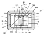
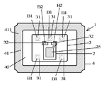
以下、本発明の実施形態について表面実装型水晶発振器を例にしながら図面を参照して説明する本発明の実施形態にかかる表面実装型水晶発振器1は、水晶振動片(圧電振動片)2と集積回路素子としてのICチップ3と、これらを配置して保持するベース4と、ベース4と接合してベース4に配置保持した水晶振動片2とICチップ3を気密封止するための蓋5とを含む構成とである。以下、この表面実装型水晶発振器の各構成について説明する。
Hereinafter, a surface-mount
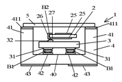
水晶振動片2は、例えばATカットの水晶片からなり、平面視矩形上の一枚板の直方体に成形されている。この水晶振動片2の両主面には、それぞれ励振電極25と、これらの励振電極25を外部電極と電気的に接続するための接続電極26と、励振電極25を接続電極に引き出すための引出電極27とが形成されている。なお、励振電極25,接続電極26,および引出電極27は、真空蒸着法やスパッタリング法により形成され、例えば、水晶振動片側からクロム、金の順か、クロム、銀の順、あるいはクロム、金、クロムの順か、クロム、銀、クロムの順、あるいはクロム、金、銀の順に積層して形成されている。なお下地電極についてはクロムにかえてニッケルなどを用いてもよい。
The
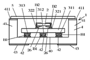
ICチップ3は、水晶振動片2とともに発振回路を構成する1チップ集積回路素子であり、水晶振動片2より平面積が大きくその底面あるいは上面に複数の接続端子が形成されている。本実施形態では、ICチップ3にベアチップを採用しており、FCB(フリップチップボンディング)工法で接続されるICチップ3を採用している。ICチップ3の底面(一方の主面)に2列に配置された後述するベース4と接続される複数の第1接続端子31が3つずつ並んで形成され、ICチップ3の上面(他方の主面)に第1接続端子と同じ並び方向で水晶振動片2と接続される少なくとも一対の第2接続端子32が形成されている。
The
より具体的には、第1接続端子としては少なくとも6つの接続端子311〜316を有しており、ICチップ3の底面の対向する2辺近傍に沿って3つの接続端子311〜313が並んだ第1の配列と3つの接続端子314〜316が並んだ第2の配列との2列に形成されている。第2接続端子としては少なくとも2つの接続端子321,322を有しており、ICチップ3の上面の1辺近傍で、上記接続端子311〜313と同じ並び方向に沿って形成されている。この時、第1接続電極311〜313と第2接続電極321,322とがお互いに平面視(ICチップの厚み方向で)重畳しない位置に形成されている。このため、後述するようなベース4に搭載されたICチップ3の上面に水晶振動片2をフリップチップボンディングする際に、第1接続電極と接合された金属バンプB1に対して再度超音波印加されることがないため、金属バンプB1が剥離するなどの不具合が生じることもない。
More specifically, the first connection terminal has at least six
なお、第1接続端子31として6つの接続端子を1列あたり3つずつ配置しているが、図4の変形例に示すように、第2接続端子が近接する列部分のみが3つ配置され5つの接続端子構造としてもよい。このように第2接続端子が近接する列位置の第1接続端子を3つ以上配置することで、後述するようなベース4に搭載されたICチップ3の上面に水晶振動片2をフリップチップボンディングする際に、超音波ボンディングツールで押圧しても3つ以上の第1接続端子の並び方向に沿ってICチップ3が厚み方向に撓むことが抑制される。結果として、2つの第2接続端子の間でICチップ3が厚み方向に撓むことがなくなり、2つの第2接続端子の形成面における平行平面度にもばらつきも生じにくくなり、ICチップ3と水晶振動片2とのフリップチップボンディング接合が安定して接合することができる。
Note that six connection terminals are arranged as three
ベース4は、全体として直方体で、アルミナ等のセラミックからなる絶縁性材料とタングステン等の導電材料を適宜積層した構成からなる。このベース4は、箱状体に形成され、セラミック材料からなる平面視矩形状の一枚板上に、所定形状からなる導電材料および中空を有するセラミック材料を積層して断面視略凹状に一体的に焼成されている。また、中空を有するセラミック材料は、平面視矩形状の一枚板のセラミック材料の表面外周に沿って成形されている。この中空が積層されて断面凹状の収納部40を構成している。収納部40の周囲には堤部41(外壁部)が形成されており、堤部41の上面は平坦で、蓋との接合領域であり、この接合領域には後述する蓋5と接合するための封止用金属層411が設けられている。
The
ベース4の収納部40の内底面には、ICチップ3の各第1接続端子と接合される複数の電極パッド42と、当該電極パッド42を外部端子電極43に延出するための外部接続用の電極パターン(図示せず)とが形成されている。これにより水晶振動片2およびICチップ3は第1端子電極31から外部(外部部品や外部機器)へと接続(接合)される。このような電極パッド42、電極パターン、外部端子電極43、および封止用金属層411は、例えばタングステンやモリブデンのメタライズ層(図示省略)の上部にニッケルメッキと金メッキが形成されている。
A plurality of
ベース4の平面視四隅を含む堤部41の外周には、複数のキャスタレーションが形成されている。キャスタレーションは、ベース4の半円弧状の切り欠き(半円弧状の凹部)が本体筐体の表面から裏面にかけて形成されている。このキャスタレーションには図示しない電極パターンが形成されている。また、ベース4の裏面には外部(外部部品や外部機器)の電極との接続(接合)される複数の外部端子電極43が形成されている。この外部端子電極43には、少なくとも、Gnd用電極と、出力用電極と、OE(Output Enable)用電極と、VDD用電極等がある。
A plurality of castellations are formed on the outer periphery of the
ベースの収納部の電極パッド42とICチップの第1接続端子311〜316とは、金などからなる金属バンプB1を介して超音波印加されフリップチップボンディング接合される。このようにベース4とICチップ3とが接合された状態で、ICチップの第2接続端子321,322と水晶振動片の接続電極26とが金属バンプB2を介して超音波印加されフリップチップボンディング接合される。この時ICチップ3より平面積が小さい水晶振動片2をICチップ3の平面視搭載領域からはみ出すことなく、ICチップ3の平面視投影面積の範囲内部に収めるように搭載し接合している。このようにしてベースの収納部40にICチップ3が接合され、ICチップ3の上面に水晶振動片2が電気的機械的に接合されている。
The
なお、ICチップの第2接続端子321,322と水晶振動片の接続電極26とを接合する金属バンプB2としては、小型化された水晶振動片に対応しやすく、かつICチップ3や水晶振動片2を損傷しにくい観点で、水晶振動片2の接続電極26に形成された金属メッキバンプを用いることが好ましい。例えば、金属メッキバンプとして金メッキが用いられ、接続電極26の端部の一部に一辺が70μm程度で平面積が4900μm2の平面視正方形状で形成されており、その厚みが5〜20μm程度で形成されている。
Note that the metal bump B2 for joining the
蓋5は、例えば金属材料からなり下面にろう材(図示省略)が形成されている。シーム溶接やビーム溶接、雰囲気加熱等の手法によりベース4に接合されて、蓋5とベース4とによる表面実装型水晶発振器の本体筐体が成形される。具体的にシーム溶接による蓋5は、コバールからなるコア材に金属層としての金属ろう材が形成された平面視矩形状の一枚板構成であり、より詳しくは、例えば上面からニッケル層、コバールコア材、銅層、銀ろう層の順の多層構成である。ここでいう銀ろう層がベース2のメタライズ層と接合される。また、銀ろう層の一部がベース4のメタライズ層と接合するための溶接領域とされ、この溶接領域は蓋の平面視外周端部に沿って設定されている。蓋5の平面視外形はベース2の外形とほぼ同じであるか、若干小さい構成となっている。
The
これらICチップ3および水晶振動片2が収納されたベース4を蓋5にて被覆し、ベース4の封止用金属層と蓋の銀ろう層の一部とを溶融硬化させて接合させ、収納部40内のICチップ3および水晶振動片2の気密封止を行う。
The
上記実施形態により、ICチップ3より平面積が小さい水晶振動片2をICチップ3の平面視搭載領域からはみ出すことなく、ICチップ3の平面視投影面積の範囲内部に収めるように搭載することができるため、ベースの収納部40はICチップ3を収納する領域だけを確保するだけでよく、水晶振動片2を保持する別領域が必要ないため、表面実装型水晶発振器の平面積の外形を小さくできる。ICチップ3の第1接続端子31とベース4の電極パッド42とが金属バンプB1を介してフリップチップボンディング接合しているので、水晶振動片2をICチップ3の上面に搭載することができ、ワイヤボンディングを用いる場合に比べてICチップ3の収納領域の小型化にも対応することができる。特に導電性樹脂接着剤で第2接続端子32と水晶振動片2の接続電極26とを接合する場合に比べて、第2接続端子321,322の間で短絡の問題が生じにくく、導電性樹脂接着剤がICチップ3の他方の主面側の第1接続端子31へ流れ出して短絡することもないので小型化に好ましい保持構成となる。フリップチップボンディング接合されたICチップ3は、搭載される際に超音波ボンディングツールにより押圧されることで、その接続端子311〜313、および314〜316の並び方向と直交する方向、特に接続端子311〜313の列と接続端子314〜316の列の間で撓むことがある。本発明では、ICチップ3の撓みにくい前記第1接続端子311〜313の並びと同じ方向に水晶振動片2の接続電極26,26が並んだ状態で金属バンプを介して接合される。このため外部からの応力も一対の接続電極26,26で均等に加わり、接合後の水晶振動片2に対してこの残部応力が加わった状態で接合されることもなくなる。結果として水晶振動片2に不要な応力が加わり特性に悪影響を与えることもない。
According to the above-described embodiment, the quartz
本発明は、その精神や主旨または主要な特徴から逸脱することなく、他のいろいろな形で実施することができる。そのため、上述の実施例はあらゆる点で単なる例示にすぎず、限定的に解釈してはならない。本発明の範囲は特許請求の範囲によって示すものであって、明細書本文には、なんら拘束されない。さらに、特許請求の範囲の均等範囲に属する変形や変更は、全て本発明の範囲内のものである。 The present invention can be implemented in various other forms without departing from the spirit, the gist, or the main features of the present invention. For this reason, the above-described embodiment is merely an example in all respects and should not be interpreted in a limited manner. The scope of the present invention is indicated by the claims, and is not restricted by the text of the specification. Further, all modifications and changes belonging to the equivalent scope of the claims are within the scope of the present invention.
本発明は、表面実装型圧電発振器に適用できる。 The present invention can be applied to a surface mount piezoelectric oscillator.
1 表面実装型水晶発振器
2 水晶振動片
3 ICチップ
4 ベース
5 蓋
DESCRIPTION OF
Claims (3)
前記圧電振動片とICチップとを収納する収納部を有し、当該収納部の上面にICチップと接続される電極パッドが形成された絶縁性のベースとを備えており、
前記圧電振動片は励振電極と接続電極と引出電極とが形成され、
前記ICチップは一方の主面に前記ベースと接続される3つ以上の第1接続端子が並んで形成された第1接続端子の配列を構成し、他方の主面に前記第1接続端子の配列における第1接続電極の並びと同じ方向で前記圧電振動片と接続される少なくとも一対の第2接続端子が並んで形成されており、
前記ベースの収納部の電極パッドと前記ICチップの第1接続端子とが金属バンプを介してフリップチップボンディング接合され、
前記ICチップの第2接続端子と前記圧電振動片の接続電極とが金属バンプを介してフリップチップボンディング接合されてなることを特徴とする表面実装型圧電発振器。 A piezoelectric vibrating piece, and an IC chip having a larger plane area than the piezoelectric vibrating piece;
A housing portion for housing the piezoelectric vibrating piece and the IC chip, and an insulating base having an electrode pad connected to the IC chip formed on an upper surface of the housing portion;
The piezoelectric vibrating piece is formed with an excitation electrode, a connection electrode, and an extraction electrode,
The IC chip constitutes an array of first connection terminals formed by arranging three or more first connection terminals connected to the base on one main surface, and the first connection terminals on the other main surface. At least a pair of second connection terminals connected to the piezoelectric vibrating reeds in the same direction as the arrangement of the first connection electrodes in the array,
The electrode pad of the storage part of the base and the first connection terminal of the IC chip are flip-chip bonded through a metal bump,
2. A surface-mount type piezoelectric oscillator comprising: a second connection terminal of the IC chip and a connection electrode of the piezoelectric vibrating piece that are flip-chip bonded through metal bumps.
Priority Applications (1)
| Application Number | Priority Date | Filing Date | Title |
|---|---|---|---|
| JP2010285552A JP2012134792A (en) | 2010-12-22 | 2010-12-22 | Surface mounted piezoelectric oscillator |
Applications Claiming Priority (1)
| Application Number | Priority Date | Filing Date | Title |
|---|---|---|---|
| JP2010285552A JP2012134792A (en) | 2010-12-22 | 2010-12-22 | Surface mounted piezoelectric oscillator |
Publications (1)
| Publication Number | Publication Date |
|---|---|
| JP2012134792A true JP2012134792A (en) | 2012-07-12 |
Family
ID=46649849
Family Applications (1)
| Application Number | Title | Priority Date | Filing Date |
|---|---|---|---|
| JP2010285552A Pending JP2012134792A (en) | 2010-12-22 | 2010-12-22 | Surface mounted piezoelectric oscillator |
Country Status (1)
| Country | Link |
|---|---|
| JP (1) | JP2012134792A (en) |
Cited By (7)
| Publication number | Priority date | Publication date | Assignee | Title |
|---|---|---|---|---|
| CN103972180A (en) * | 2013-01-30 | 2014-08-06 | 精工爱普生株式会社 | Method of manufacturing electronic device, electronic device, electronic apparatus, and moving object |
| JP2014146735A (en) * | 2013-01-30 | 2014-08-14 | Seiko Epson Corp | Method for manufacturing electronic device |
| US10784835B2 (en) | 2017-11-29 | 2020-09-22 | Seiko Epson Corporation | Vibration device, electronic apparatus, and vehicle |
| US11277111B2 (en) | 2017-12-26 | 2022-03-15 | Seiko Epson Corporation | Vibrator device, electronic apparatus, and vehicle |
| CN116346077A (en) * | 2021-12-24 | 2023-06-27 | 精工爱普生株式会社 | Vibration device and method for manufacturing the vibration device |
| US11990887B2 (en) | 2020-04-22 | 2024-05-21 | Seiko Epson Corporation | Vibrator device and vibrator module |
| JP2025103043A (en) * | 2021-03-01 | 2025-07-08 | 株式会社大真空 | Thermostatic oven type piezoelectric oscillator |
-
2010
- 2010-12-22 JP JP2010285552A patent/JP2012134792A/en active Pending
Cited By (9)
| Publication number | Priority date | Publication date | Assignee | Title |
|---|---|---|---|---|
| CN103972180A (en) * | 2013-01-30 | 2014-08-06 | 精工爱普生株式会社 | Method of manufacturing electronic device, electronic device, electronic apparatus, and moving object |
| JP2014146735A (en) * | 2013-01-30 | 2014-08-14 | Seiko Epson Corp | Method for manufacturing electronic device |
| US10784835B2 (en) | 2017-11-29 | 2020-09-22 | Seiko Epson Corporation | Vibration device, electronic apparatus, and vehicle |
| US11277111B2 (en) | 2017-12-26 | 2022-03-15 | Seiko Epson Corporation | Vibrator device, electronic apparatus, and vehicle |
| US11990887B2 (en) | 2020-04-22 | 2024-05-21 | Seiko Epson Corporation | Vibrator device and vibrator module |
| JP2025103043A (en) * | 2021-03-01 | 2025-07-08 | 株式会社大真空 | Thermostatic oven type piezoelectric oscillator |
| JP7761172B2 (en) | 2021-03-01 | 2025-10-28 | 株式会社大真空 | Oven-type piezoelectric oscillator |
| CN116346077A (en) * | 2021-12-24 | 2023-06-27 | 精工爱普生株式会社 | Vibration device and method for manufacturing the vibration device |
| US20230208388A1 (en) * | 2021-12-24 | 2023-06-29 | Seiko Epson Corporation | Vibrator device and method for manufacturing vibrator device |
Similar Documents
| Publication | Publication Date | Title |
|---|---|---|
| JP5853429B2 (en) | Electronic component package and piezoelectric vibration device | |
| JP6020663B2 (en) | Oscillator | |
| JP4552916B2 (en) | Piezoelectric vibration device | |
| JP2012134792A (en) | Surface mounted piezoelectric oscillator | |
| JP2009065437A (en) | Crystal device | |
| JP2012090202A (en) | Piezoelectric device and piezoelectric oscillator | |
| JP5082968B2 (en) | Piezoelectric oscillator | |
| JP4784055B2 (en) | Piezoelectric oscillator | |
| JP5098668B2 (en) | Surface mount type piezoelectric oscillator | |
| JP4899519B2 (en) | Surface mount type piezoelectric oscillator | |
| JP2004320297A (en) | Piezoelectric vibration device | |
| JP6538401B2 (en) | Piezoelectric device and method of manufacturing the same | |
| JP2006054602A (en) | Electronic component package and piezoelectric vibration device using the electronic component package | |
| JP4501875B2 (en) | Piezoelectric vibration device and manufacturing method thereof | |
| JP2010200230A (en) | Crystal oscillator for surface mounting | |
| JP2008259004A (en) | Piezoelectric device and manufacturing method thereof | |
| JP2013239790A (en) | Surface mount type piezoelectric oscillator | |
| JP2005268257A (en) | Electronic component storage package and electronic device | |
| JP2012070258A (en) | Surface-mount type piezoelectric vibration device | |
| JP5310418B2 (en) | Surface mount type piezoelectric oscillator | |
| JP2009239475A (en) | Surface mounting piezoelectric oscillator | |
| JP2010283650A (en) | Piezoelectric oscillator | |
| JP2011018951A (en) | Piezoelectric oscillator | |
| JP2014187641A (en) | Surface mounting piezoelectric oscillator | |
| JP5716594B2 (en) | Piezoelectric vibration device |