JP2012127761A - Substrate inspection device - Google Patents
Substrate inspection device Download PDFInfo
- Publication number
- JP2012127761A JP2012127761A JP2010278637A JP2010278637A JP2012127761A JP 2012127761 A JP2012127761 A JP 2012127761A JP 2010278637 A JP2010278637 A JP 2010278637A JP 2010278637 A JP2010278637 A JP 2010278637A JP 2012127761 A JP2012127761 A JP 2012127761A
- Authority
- JP
- Japan
- Prior art keywords
- substrate
- air
- inspection
- light
- optical system
- Prior art date
- Legal status (The legal status is an assumption and is not a legal conclusion. Google has not performed a legal analysis and makes no representation as to the accuracy of the status listed.)
- Pending
Links
Images


Landscapes
- Investigating Materials By The Use Of Optical Means Adapted For Particular Applications (AREA)
Abstract
Description
本発明は、表示用パネル等の製造に用いられるガラス基板やプラスチック基板等の欠陥を製造ライン上で検査するための基板検査装置に関する。 The present invention relates to a substrate inspection apparatus for inspecting defects on a production line such as a glass substrate and a plastic substrate used for manufacturing a display panel or the like.
表示用パネルとして用いられる液晶ディスプレイ装置のTFT(Thin Film Transistor)基板やカラーフィルタ基板、プラズマディスプレイパネル用基板、有機EL(Electro Luminescence)表示パネル用基板等の製造は、フォトリソグラフィー技術によって、ガラス基板やプラスチック基板等の上にパターンを形成して行われる。その際、基板に傷や異物等の欠陥が存在すると、パターンが良好に形成されず、不良の原因となる。このため、基板検査装置を用いて、基板の傷や異物等の欠陥の検査が行われている。 Manufacture of TFT (Thin Film Transistor) substrates, color filter substrates, plasma display panel substrates, organic EL (Electro Luminescence) display panel substrates, etc. for liquid crystal display devices used as display panels is a glass substrate by photolithography technology. Or by forming a pattern on a plastic substrate or the like. At that time, if a defect such as a scratch or a foreign substance exists on the substrate, the pattern is not formed well, which causes a defect. For this reason, a substrate inspection apparatus is used to inspect defects such as scratches and foreign matter on the substrate.
基板検査装置は、レーザー光等の検査光を基板へ照射し、基板からの反射光又は散乱光を受光して、基板の傷や異物等の欠陥を検出するものである。検査光によって基板を走査するため、基板全体の検査には時間が掛かる。そのため、従来は、ガラス基板やプラスチック基板等の製造ライン上や、これらの基板等を用いた表示用パネル基板の製造ライン上で、基板の欠陥をリアルタイムに検査することは困難であった。そこで、特許文献1に記載されたもののように、インライン上でガラス基板ごとにカメラでスキャンされた一部の単位領域に対するパーティクルの情報をデータ化して、ガラス基板のそれぞれの全領域に対するパーティクルの情報を統計的な数値で表示することによってガラス基板全体のパーティクル情報を測定する方法が提案されている。
The substrate inspection apparatus irradiates a substrate with inspection light such as laser light and receives reflected light or scattered light from the substrate to detect defects such as scratches or foreign matter on the substrate. Since the substrate is scanned with the inspection light, it takes time to inspect the entire substrate. Therefore, conventionally, it has been difficult to inspect for defects in a substrate in real time on a production line for a glass substrate, a plastic substrate or the like, or on a production line for a display panel substrate using these substrates. Therefore, as described in
従来の典型的な異物検査装置は、生産ラインから別個独立した形式で運用されてきたものが多く、検査測定を行う場合に、生産ラインからガラス基板を抜き取り、搬送装置等を使用して検査装置に投入して検査する必要があった。ガラス基板は、全面を検査することが一般的となっており、搬送・検査動作及び検査処理にかかる演算等に多大な時間を必要とし、生産ラインから一旦ガラス基板を抜き取らなければならないという面で、稼動管理面からすると非効率的であった。また、ガラス基板内の局所的な位置の測定をする際にも、従来の検査装置では、わざわざ全面検査を行なう必要があり、この点からも無駄な時間を費やす結果となっていた。 Many conventional conventional foreign matter inspection devices have been operated in a separate and independent form from the production line, and when performing inspection and measurement, the glass substrate is extracted from the production line and the inspection device is used using a transfer device or the like. It was necessary to put it in and inspect it. It is common to inspect the entire surface of a glass substrate, which requires a lot of time for operations such as transport / inspection operations and inspection processing, and the glass substrate must be extracted from the production line once. In terms of operation management, it was inefficient. Further, when measuring a local position in the glass substrate, the conventional inspection apparatus has to bother to perform a full inspection, and this also results in wasted time.
そこで、本願出願人は、ライン内での基板の欠陥の検査をより迅速に行うことを目的として、特許文献2に記載の発明を出願した。特許文献2に記載の発明は、検出した走査領域の基板の欠陥のデータを、走査領域毎に記憶し、基板毎に、新たに検出した走査領域の基板の欠陥のデータによって、記憶された同じ走査領域の基板の欠陥のデータを更新して、複数の走査領域の基板の欠陥のデータから、基板1枚分の欠陥のデータを作成することによって、基板1枚分の欠陥のデータを基板毎に得ることができるので、ライン内での基板の欠陥の検査をより迅速に行うようにしたものである。この特許文献2に記載された基板検査装置は、2系列分の光学系を設け、それぞれの光学系に対して複数の開口部を設け、2系列分の開口部の配置をそれぞれ千鳥状にすることによって、迅速な検査を行なうようにしている。ところが、ガラス基板を移動方向(X方向)へ移動させるステージの上面には、複数のエア吹き出し口が設けられているので、2系列分の光学系のそれぞれに開口部を設けることは検査エリアにおいてエア吹き出し口が減少することとなり、ガラス基板の自重による撓み等が大きくなり、面精度が粗くなり、高精度の検査の妨げとなる可能性があった。また、特許文献2に記載の基板検査装置は、高価な光学系を2系列分設ける必要があった。 Accordingly, the applicant of the present application has applied for the invention described in Patent Document 2 for the purpose of promptly inspecting defects in the substrate within the line. The invention described in Patent Document 2 stores the detected defect data of the substrate in the scanning region for each scanning region, and stores the same data stored for each substrate by the newly detected substrate defect data in the scanning region. By updating the defect data of the substrate in the scanning region and generating defect data for one substrate from the defect data of the substrate in a plurality of scanning regions, the defect data for one substrate is generated for each substrate. Therefore, the inspection of the defect of the substrate in the line can be performed more quickly. The substrate inspection apparatus described in Patent Document 2 includes two series of optical systems, a plurality of openings for each optical system, and the arrangement of the two series of openings is staggered. By doing so, a quick inspection is performed. However, since a plurality of air outlets are provided on the upper surface of the stage that moves the glass substrate in the movement direction (X direction), it is necessary to provide openings in each of the two systems of optical systems in the inspection area. The number of air outlets will be reduced, the deflection of the glass substrate due to its own weight will increase, the surface accuracy will become rough, and this may hinder high-precision inspection. Further, the substrate inspection apparatus described in Patent Document 2 needs to provide two expensive optical systems.
この発明は、基板搬送時のエア浮上を安定化させることによって検査精度を向上することのできる基板検査装置を提供することを目的とする。 An object of this invention is to provide the board | substrate inspection apparatus which can improve a test | inspection precision by stabilizing the air floating at the time of board | substrate conveyance.
本発明に係る基板検査装置の第1の特徴は、基板の下面にエア吹き出し口からエア噴流を吹き付けることによって前記基板をエア浮上させながら上流ラインから下流ラインヘ移動させるエア浮上ステージ手段と、投光系及び受光系からなる光学系手段を移動させて前記基板の所定の箇所に検査光を照射すると共に前記基板からの反射光又は散乱光を受光し、受光した前記基板からの反射光又は散乱光に基づいて前記基板の欠陥を検査する基板検査手段とを備えた基板検査装置において、前記光学系手段から前記基板に照射される検査光を通過させるための複数の開口部とこの開口部以外の箇所に前記エア吹き出し口を備えたエア噴出シフト板手段であって、前記基板の移動方向に対して垂直方向にシフト移動可能に構成されたエア噴出シフト板手段を、前記エア浮上ステージ手段の途中の前記光学系手段による検査エリアに設け、前記エア噴出シフト板手段をシフト移動させると共に前記光学系手段を前記開口部に対応付けて移動させることによって前記基板の所定の領域の欠陥を検査するようにしたことにある。
この発明に係る基板検査装置は、上流ラインから下流ラインヘ基板を順番にエア浮上移動させる流動的な生産ライン上の検査エリアで1枚1枚のガラス基板に対し、所定の走査領域分の測定を行なう。エア浮上ステージ手段の途中に検査光を通過させるための開口となるギャップを設けると、そのギャップの設けられた箇所には吹き出し口が存在しなくなり、そこをエア浮上中の基板が通過するときに、ギャップに基板の先端などがひっかかることとなり、安定したエア浮上搬送を行なうことができなくなるおそれがあった。そこで、この発明では、検査光を通過させる複数の開口部を備えたエア噴出シフト板手段をエア浮上ステージ手段の途中の検査エリアに、基板の移動方向に対して垂直方向にシフト移動可能に設け、エア噴出シフト板手段をシフト移動させると共に光学系手段を開口部に対応付けて移動させることによって基板の所定の領域の欠陥を検査するようにした。これによって、搬送中の基板が安定してエア浮上されるようになり、検査精度を向上させることが可能となる。
A first feature of the substrate inspection apparatus according to the present invention is that air floating stage means for moving the substrate from the upstream line to the downstream line while blowing the air jet from the air blowing port to the lower surface of the substrate and projecting light is provided. An optical system means comprising a system and a light receiving system is moved to irradiate a predetermined portion of the substrate with inspection light, receive reflected light or scattered light from the substrate, and receive the reflected light or scattered light from the substrate A substrate inspection apparatus comprising: a substrate inspection device for inspecting a defect of the substrate based on the plurality of openings for passing the inspection light applied to the substrate from the optical system means; Air jet shift plate means provided with the air outlet at a location, wherein the air jet shift is configured to be shiftable in a direction perpendicular to the moving direction of the substrate Means is provided in an inspection area by the optical system means in the middle of the air levitation stage means, the air ejection shift plate means is shifted and the optical system means is moved in association with the opening. In other words, a defect in a predetermined area is inspected.
The substrate inspection apparatus according to the present invention performs measurement for a predetermined scanning region on each glass substrate in an inspection area on a fluid production line in which the substrate is sequentially levitated and moved from the upstream line to the downstream line. Do. When a gap serving as an opening for allowing inspection light to pass therethrough is provided in the middle of the air levitation stage means, there is no air outlet at the position where the gap is provided, and when the air levitation substrate passes therethrough As a result, the tip of the substrate gets caught in the gap, and there is a risk that stable air levitation transfer cannot be performed. Therefore, in the present invention, an air ejection shift plate means having a plurality of openings through which inspection light passes is provided in the inspection area in the middle of the air levitation stage means so as to be shiftable in a direction perpendicular to the moving direction of the substrate. Then, the air ejection shift plate means is shifted and the optical system means is moved in correspondence with the opening, thereby inspecting a defect in a predetermined region of the substrate. As a result, the substrate being transported stably floats on the air, and the inspection accuracy can be improved.
本発明に係る基板検査装置の第2の特徴は、前記第1の特徴に記載の基板検査装置において、前記エア浮上ステージが、前記基板の移動方向に対して垂直な方向に分割された長尺状の複数のエア噴出板手段から構成されることにある。これは、エア浮上ステージを分割された複数のエア噴出板で構成することによって、エア噴出孔から噴出されたエアを各エア噴出板の間から効率的に排出するためである。なお、エア噴出板に多数の細孔からなるエア噴出孔を千鳥状に設け、噴出エアを吸着するエア吸着孔をこの噴出孔とそれぞれ交互となるように千鳥状に配置してもよい。 A second feature of the substrate inspection apparatus according to the present invention is the substrate inspection device according to the first feature, wherein the air levitation stage is divided in a direction perpendicular to the moving direction of the substrate. A plurality of air ejection plate means. This is because the air ejected from the air ejection plates is efficiently discharged from the air ejection plates by configuring the air levitation stage with a plurality of divided air ejection plates. The air ejection plate may be provided with air ejection holes made up of a large number of pores in a zigzag pattern, and the air adsorption holes for adsorbing the ejection air may be arranged in a zigzag pattern so as to alternate with the ejection holes.
本発明に係る基板検査装置の第3の特徴は、前記第1又は第2の特徴に記載の基板検査装置において、前記エア噴出シフト板手段が、1回シフト移動することによって前記基板の全走査領域の検査に対応することができる数の前記開口部を備えたことにある。これは、エア噴出シフト板手段に設けられる開口数の数を規定したものであり、1回のシフト移動によって基板の全走査領域をカバーすることができるようにしたものである。 A third feature of the substrate inspection apparatus according to the present invention is the substrate inspection device according to the first or second feature, wherein the air ejection shift plate means shifts once to perform full scanning of the substrate. The number of the openings that can correspond to the inspection of the area is provided. This prescribes the number of numerical apertures provided in the air ejection shift plate means so that the entire scanning region of the substrate can be covered by one shift movement.
本発明に係る基板検査装置の第4の特徴は、前記第1、第2又は第3の特徴に記載の基板検査装置において、前記エア浮上ステージ手段が、前記基板の片辺又は両辺を保持した状態で前記基板を移動させることにある。これは、エア浮上ステージ手段が搬送する際に基板の片辺又は両辺を保持(挟持)することを明確にしたものである。なお、保持の方法には、基板表面に垂直な方向に対してその移動を拘束するようなボールベアリングを用いた接触保持方式やエア噴流を用いた非接触保持方式などを用いてもよい。 According to a fourth feature of the substrate inspection apparatus of the present invention, in the substrate inspection apparatus according to the first, second or third feature, the air levitation stage means holds one side or both sides of the substrate. The substrate is moved in a state. This clarifies that one side or both sides of the substrate are held (clamped) when the air levitation stage means is transported. As a holding method, a contact holding method using a ball bearing that restricts the movement in a direction perpendicular to the substrate surface, a non-contact holding method using an air jet, or the like may be used.
本発明に係る基板検査装置の第5の特徴は、基板の下面にエア吹き出し口からエア噴流を吹き付けることによって前記基板をエア浮上させながら上流ラインから下流ラインヘ移動させるエア浮上ステージ手段と、投光系及び受光系からなる光学系手段を移動させて前記基板の所定の箇所に検査光を照射すると共に前記基板からの反射光又は散乱光を受光し、受光した前記基板からの反射光又は散乱光に基づいて前記基板の欠陥を検査する基板検査手段とを備えた基板検査装置において、前記光学系手段は、前記基板の移動方向に対して所定の傾斜角度を持って移動されることによって前記基板の所定の箇所に検査光を照射し、前記エア浮上ステージは、前記基板の移動方向に対して垂直な方向に分割され、前記光学系手段から前記基板に照射される検査光を通過させるためのギャップを備えた長尺状の複数のエア噴出板手段で構成されたことにある。これは、エア浮上ステージ手段を構成する複数のエア噴出板手段に、光学系手段から前記基板に照射される検査光を通過させるためのギャップを設けると、そのギャップ付近で搬送中の基板に対して浮上エアが吹き付けられなくなり、そのギャップに基板がひっかかったりしてダメージを受けるおそれがあるので、複数のエア噴出板手段に設けるギャップを基板の進行方向に対して所定の傾斜角度となるようにした。光学系手段の移動方向もこの傾斜したギャップに併せて移動させる。これによって、基板の搬送方向の先端部がギャップにひっかかることはなくなり、基板のスムースな搬送が可能となる。 According to a fifth aspect of the substrate inspection apparatus of the present invention, there is provided an air levitation stage means for moving the substrate from an upstream line to a downstream line while blowing the air jet from an air outlet to the lower surface of the substrate, and projecting light. An optical system means comprising a system and a light receiving system is moved to irradiate a predetermined portion of the substrate with inspection light, receive reflected light or scattered light from the substrate, and receive the reflected light or scattered light from the substrate And a substrate inspection apparatus for inspecting a defect of the substrate based on the optical system means, the optical system means being moved at a predetermined inclination angle with respect to the movement direction of the substrate. And the air levitation stage is divided in a direction perpendicular to the moving direction of the substrate, and the substrate is irradiated from the optical system means. Is that constituted by elongated plurality of air ejection plate means having a gap for passing the inspection light. This is because when a plurality of air ejection plate means constituting the air levitation stage means are provided with a gap for allowing the inspection light irradiated from the optical system means to the substrate to pass therethrough, the substrate being conveyed in the vicinity of the gap. As a result, the floating air cannot be blown, and the substrate may get caught in the gap and be damaged, so the gaps provided in the plurality of air ejection plate means have a predetermined inclination angle with respect to the traveling direction of the substrate. did. The moving direction of the optical system means is also moved along with the inclined gap. As a result, the front end of the substrate in the transport direction is not caught in the gap, and the substrate can be transported smoothly.
本発明に係る基板検査装置の第6の特徴は、前記第5の特徴に記載の基板検査装置において、前記エア浮上ステージ手段は、前記基板の片辺又は両辺を保持した状態で前記基板を移動させることにある。これは、エア浮上ステージ手段が搬送する際に基板の片辺又は両辺を保持(挟持)することを明確にしたものである。なお、保持の方法には、基板表面に垂直な方向に対してその移動を拘束するようなボールベアリングを用いた接触保持方式やエア噴流を用いた非接触保持方式などを用いてもよい。 A sixth feature of the substrate inspection apparatus according to the present invention is the substrate inspection device according to the fifth feature, wherein the air levitation stage means moves the substrate while holding one or both sides of the substrate. There is to make it. This clarifies that one side or both sides of the substrate are held (clamped) when the air levitation stage means is transported. As a holding method, a contact holding method using a ball bearing that restricts the movement in a direction perpendicular to the substrate surface, a non-contact holding method using an air jet, or the like may be used.
この発明によれば、基板搬送時のエア浮上を安定化させることによって検査精度を向上することができるという効果を有する。 According to the present invention, there is an effect that the inspection accuracy can be improved by stabilizing the air levitation during the conveyance of the substrate.
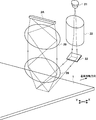
以下、本発明の一実施形態を図面に基づいて説明する。図1は、本発明の一実施の形態による基板検査装置を上から見た上面図、図2は本発明の一実施の形態による基板検査装置を横から見た図である。基板検査装置は、エア浮上ステージ10、片側チャック11,12、チャック支持駆動部13、フレーム14a,14b、光学系ユニット20、焦点調節機構41、センサー51、及び制御部(図1及び図2では図示しておらず)を含んで構成される。なお、以下に説明する実施の形態におけるXY方向は例示であって、X方向とY方向とを入れ替えてもよい。
Hereinafter, an embodiment of the present invention will be described with reference to the drawings. FIG. 1 is a top view of a substrate inspection apparatus according to an embodiment of the present invention as viewed from above, and FIG. 2 is a view of the substrate inspection apparatus according to an embodiment of the present invention as viewed from the side. The substrate inspection apparatus includes an
図1及び図2において、検査対象である複数の基板1a,1bは、ライン内において、図1及び図2の右側に位置する図示していない搬入コンベアによって基板検査装置のエア浮上ステージ10上へ順番に搬入され、片側チャック11,12に基板1a,1bのそれぞれ片辺が保持された状態で移動され、検査エリアを通過することによって検査されるようになっている。検査後は、図1及び図2の左側に位置する図示していない搬出コンベアによって基板検査装置から順番に搬出される。
1 and 2, a plurality of
エア浮上ステージ10は、複数の第1〜第5のエア噴出板101〜105と、複数の第6〜第10のエア噴出板106〜110とから構成される長尺状の分割型のステージで構成される。これらの長尺状のエア噴出板101〜110の表面には、全面に渡って多数の細孔からなるエア噴出孔が設けられている。第1〜第5のエア噴出板101〜105は検査エリアの右側に位置し、第6〜第10のエア噴出板106〜110は検査エリアの左側に位置し、検査エリアのY方向の幅寸法とほぼ同じ幅となるように構成され、Y方向において、それぞれ所定の間隔だけ離れた位置に配置されている。エア浮上ステージ10が複数のエア噴出板101〜110に分割されているのは、エア噴出孔から噴出されたエアが各エア噴出板101〜110の間から効率的に排出されるようにするためである。
The
図1おいて、エア浮上ステージ10の第5のエア噴出板105と第10のエア噴出板110の下側の隣接した位置の側面には、片側チャック11,12をX方向に移動可能に備えたチャック支持駆動部13が設けられている。エア浮上ステージ10は、図示していない搬入コンベアから各基板1a,1bを順次受け取り、片側チャック11,12によって基板1a,1bの片辺を保持して検査エリアを通過させるようにX方向に搬送移動する。片側チャック11,12は、基板1a,1bの搬送方向に沿った辺の一方側(図1における基板1a,1bの下辺側)を挟持する。チャック支持駆動部13は、片側チャック11,12に挟持された基板1a,1bを検査エリアを通過移動させる。この移動に同期させて検査エリアでは、片側チャック11,12に保持されエア浮上搬送される基板1a,1bに光学系ユニット20が検査光を照射して所定の検査処理を行う。
In FIG. 1, one-side chucks 11 and 12 are provided on the side surfaces of the
図1及び図2に示すように、エア浮上ステージ10の片側チャック11,12によってX方向に移動される基板1a,1bの上方(図1の図面奥行き方向の手前側、図2の上側)には、基板1a,1bの基板移動方向(X方向)と略直交する方向(Y方向)の幅以上に渡って伸びるフレーム14a,14bが設置されている。このフレーム14a,14bには、光学系ユニット20をY方向に移動させる光学系移動機構が搭載されている。
As shown in FIGS. 1 and 2, above the
図3及び図4は、図1及び図2のエア浮上ステージを上側から見た上面図である。すなわち、図3は、図1からフレーム14a,14b、光学系ユニット20、焦点調節機構41、センサー51を除いたエア浮上ステージ10の構成のみを示すものである。エア浮上ステージ10には、光学系ユニット20の投光系からの検査光が照射される領域に、複数の開口部が設けられていなければならない。この実施の形態では、図3に示すように、エア浮上ステージ10を構成する第1〜第5のエア噴出板101〜105と、第6〜第10のエア噴出板106〜110との間に、光学系ユニット20の検出光及び受光光を通過させるための複数の開口部を備えたエア噴出シフト板111が設けられている。
3 and 4 are top views of the air levitation stage of FIGS. 1 and 2 as viewed from above. 3 shows only the configuration of the
このエア噴出シフト板111は、図の上下方向(Y方向)にシフト移動可能なように構成されている。図3は、エア噴出シフト板111が第5のエア噴出板105と第10のエア噴出板110の下側端部に位置するようにシフトした状態を示し、図4は、逆にエア噴出シフト板111が第1のエア噴出板101と第6のエア噴出板106の上側端部に位置するようにシフトした状態を示す。図3のエア噴出シフト板111の開口部間に、図4のエア噴出シフト板111の開口部が位置するように、エア噴出シフト板111はY方向にシフトされる。これは、光学系ユニット20がシフト前後のこれらの開口部を介して基板1a,1bの全面を検出光を照射しその反射光などを受光することができるようにするためである。エア噴出シフト板111の上面の開口部以外には、図示しない複数のエア吹き出し口が設けられている。これらの複数のエア吹き出し口は、移動される各基板1a,1bの裏面に対してエアを吹き付るようになっている。各基板1a,1bに吹き付けられるエアの働きによって、エア噴出シフト板111を通過する時にも基板1a,1bは撓むことなく浮上され、X方向に順次に移動するようになる。
The air
図5は、2つの光学系をY方向に移動させる光学系移動機構の概略構成を示す一部断面側面図である。光学系移動機構は、ガイド15,17、移動台16、並びに磁石板18及びコイル19から成るリニアモータを含んで構成される。断面形状が略L字型のフレーム14a,14bには、図5の図面奥行き方向(Y方向)へ伸びるガイド15が光学系ユニット20を挟むように設けられている。それぞれのガイド15の上側には、移動台16の収納部16cが搭載される。
FIG. 5 is a partial cross-sectional side view showing a schematic configuration of an optical system moving mechanism that moves two optical systems in the Y direction. The optical system moving mechanism includes
移動台16は、光学系ユニット20を収納する凹形の収納部16cと、この収納部16cの上端部から水平方向に伸びるアーム部16dとから構成される。収納部16cには、後述する焦点調節機構41を介して、光学系ユニット20が収納搭載される。フレーム14aの上面部両側には、図5の図面奥行き方向(Y方向)へ伸びるガイド17が設けられている。それぞれのガイド17の上側には、移動台16のアーム部16dが搭載される。
The movable table 16 includes a
フレーム14aの上面部中央には、リニアモータの固定子である磁石板18が取り付けられている。移動台16のアーム部16dの下側には、リニアモータの可動子であるコイル19が取り付けられている。後述する光学系移動制御回路60からコイル19へ電流を流すと、コイル19の電流と磁石板18の磁界とから、フレミングの左手の法則によって、コイル19に推力(ローレンツ力)が働き、移動台16がガイド15及びガイド17に沿って移動し、光学系ユニット20が基板移動方向(X方向)と直交する図面奥行き方向(Y方向)へ移動制御される。
A
図6は、光学系の投光系及び受光系の概略構成を示す斜視図である。図7は、光学系及び制御部の概略構成を示す図である。光学系ユニット20は、検査光を基板1aへ照射する投光系、基板1aからの反射光を検出する反射光検出系、及び基板1aからの散乱光を受光する受光系を含んで構成される。また、制御系は、焦点調節制御回路40、信号処理回路50、光学系移動制御回路60、メモリ70、通報装置80、入出力装置90及びCPU100を含んで構成される。
FIG. 6 is a perspective view showing a schematic configuration of a light projecting system and a light receiving system of the optical system. FIG. 7 is a diagram illustrating a schematic configuration of the optical system and the control unit. The
図に示すように、投光系は、レーザー光源21、レンズ群22及びミラー23を含んで構成される。レーザー光源21は、検査光となるレーザー光を発生する。レンズ群22は、レーザー光源21から発生された検査光を集光し、集光した検査光を基板移動方向(X方向)と直交する方向(Y方向)へ広げ、広げた検査光を基板移動方向(X方向)に集束させる。ミラー23は、レンズ群22によって集光された検査光を、基板1の表面に斜めに照射する。基板1の表面に照射された検査光は、基板1の表面上において、基板移動方向(X方向)に集束し、基板移動方向(X方向)と直交する方向(Y方向)に所定の幅を持った長尺状の検査光となる。基板1が基板移動方向(X方向)へ移動することにより、投光系から照射された所定の幅の検査光が基板1を走査することとなり、走査領域の欠陥の検査が行われる。
As shown in the figure, the light projecting system includes a
基板1の表面に傷や異物等の欠陥が存在しない場合は、基板1の表面に斜めに照射された検査光の一部は基板1の表面で反射し、残りの検査光は基板1の内部を透過して基板1の裏面から射出する。基板1の表面に傷や異物等の欠陥がある場合は、基板1の表面に照射された検査光の中で基板表面の傷や異物等の欠陥に照射された光は散乱光して散乱し、以外の箇所に照射した光は前述と同様に、一部は表面で反射し、残りは透過する。
When there are no defects such as scratches or foreign matter on the surface of the
図7において、反射光検出系は、ミラー25、レンズ26、及びCCDラインセンサー27を含んで構成される。基板1の表面からの反射光は、ミラー25を介してレンズ26に入射する。レンズ26は、基板1からの反射光を集束させ、CCDラインセンサー27の受光面に結像させる。
In FIG. 7, the reflected light detection system includes a
このとき、CCDラインセンサー27の受光面における反射光の受光位置は、基板1の表面の高さによって変化する。図7に示す基板1の表面の高さを基準としたとき、基板1の表面の高さが基準より低い場合、基板1の表面で検査光が照射及び反射される位置が図面の左側へ移動し、CCDラインセンサー27の受光面における反射光の受光位置が図面の右側へ移動する。逆に、基板1の表面の高さが基準より高い場合、基板1の表面で検査光が照射及び反射される位置が図面の右側へ移動し、CCDラインセンサー27の受光面における反射光の受光位置が図面の左側へ移動する。
At this time, the light receiving position of the reflected light on the light receiving surface of the
CCDラインセンサー27は、受光面で受光した反射光の強度に応じた検出信号を、焦点調節制御回路40へ出力する。焦点調節制御回路40は、CPU100からの指令に従って、CCDラインセンサー27の検出信号に基づき、基板1の表面からの反射光がCCDラインセンサー27の受光面の中心位置で受光されるように、焦点調節機構41を駆動して光学系ユニット20を移動する。焦点調節機構41は、パルスモータ42、カム43、及びカムフォロア44を含んで構成される。パルスモータ42の回転軸には、偏心したカム43が取り付けられており、光学系ユニット20には、カムフォロア44が取り付けられている。焦点調節制御回路40からパルスモータ42へ駆動パルスを供給することにより、パルスモータ42が駆動されてカム43が回転し、光学系ユニット20が上下に移動されて、光学系ユニット20の焦点位置が制御される。
The
図6において、光学系ユニット20の投光系から照射され、基板1の内部へ透過して基板1の裏面から射出された検査光は、エア噴出シフト板111の開口部を通ってステージ10の下方へ進み、光学系ユニット20の反射光検出系及び受光系で受光されない。光学系ユニット20の投光系から照射され、基板1の内部へ透過して基板1の裏面から射出された検査光も、同様に、開口を通ってステージ10の下方へ進み、光学系ユニット20の反射光検出系及び受光系で受光されない。
In FIG. 6, the inspection light emitted from the light projecting system of the
図6及び図7において、受光系は、集光レンズ28、結像レンズ29、及びCCDラインセンサー2Aを含んで構成される。集光レンズ28は、基板1からの散乱光を集光し、結像レンズ29は、集光レンズ28で集光された散乱光をCCDラインセンサー2Aの受光面に結像させる。図6において、CCDラインセンサー2Aは、受光面で受光した散乱光の強度に応じた検出信号をディジタル信号に変換して、信号処理回路50へ出力する。
6 and 7, the light receiving system includes a
図7において、光学系移動制御回路60は、CPU100からの指令に従って、コイル19へ電流を供給し、光学系ユニット20を基板移動方向(X方向)と直交する方向(Y方向)へ移動して、光学系ユニット20の投光系からの所定の幅の検査光により走査される基板1の走査領域すなわちエア噴出シフト板111の開口部を基板毎に変更する。
In FIG. 7, the optical system
図8は、基板の走査領域の一例を示す図である。本実施の形態は、基板1aの検査領域を24個の走査領域に分割し、2つの光学系ユニット20を用いて、それぞれ22回ずつの走査を行う例を示している。なお、走査領域の数及び走査回数は、これに限らず、基板の大きさや光学系の数に応じて適宜決定される。
FIG. 8 is a diagram illustrating an example of the scanning region of the substrate. This embodiment shows an example in which the inspection area of the
図7において、走査領域SA1〜SA12,SB1〜SB12は、光学系ユニット20の走査領域である。本実施の形態では、まず、図3のようにエア噴出シフト板111を位置させ、1枚目の基板1aがセンサー51の下方へ達する前に、光学系ユニット20を走査領域SA1が通過する位置(エア噴出シフト板111の最下段の開口部)の上空へ移動する。そして、1枚目の基板1aについて、光学系ユニット20の投光系からの検査光によって、走査領域SA1の走査を行なう。1枚目の基板にに対して走査領域SA1の走査が終了した後、2枚目の基板1bが後述するセンサー51の下方へ達する前に、光学系ユニット20を走査領域SA2が通過する位置(エア噴出シフト板111の下から2段目の開口部)の上空へ移動する。そして、2枚目の基板1bについて、光学系ユニット20の投光系からの検査光により、走査領域SA2の走査を行い、以後、これらの動作を繰り返し、12枚目の基板について、光学系ユニット20の投光系からの検査光により、エア噴出シフト板111の各開口部に対応するように走査領域SA12までの走査を行う。12枚目の基板に対する走査が終了した後は、図4のようにエア噴出シフト板111を位置させ、13枚目〜24枚目の基板に対する走査を同様に行なう。なお、上述の走査の順序は一例であり、図3及び図4の位置にエア噴出シフト板111を交互に位置させるようにして、走査領域SA1,SB1,SA2,SB2,・・・・のように順番に走査を行なってもよい。また、走査領域SA1〜SA12の走査の後に、光学系ユニット20を逆方向へ移動して、走査領域SB12から走査領域SB1に向かって走査を行なっても良い。
In FIG. 7, scanning areas SA1 to SA12 and SB1 to SB12 are scanning areas of the
図1及び図2において、センサー51は、エア浮上移動される基板1aの基板移動方向側の縁を検出し、検出信号を図7の信号処理回路50へ出力する。図7において、信号処理回路50は、CCDラインセンサー2Aからのディジタル信号を処理して、走査領域の基板1の欠陥を、予め定めた大きさのランク別に検出し、検出した欠陥の走査領域内での基板移動方向(X方向)と直交する方向(Y方向)の位置を検出する。信号処理回路50は、また、センサー51から検出信号を入力してからの経過時間に基づき、検出した欠陥の基板移動方向(X方向)の位置を検出する。信号処理回路50は、検出した欠陥のデータを、CPU100へ出力する。
1 and 2, the
図7において、メモリ70は、CPU100の制御により、信号処理回路50が検出した走査領域の基板1の欠陥のデータを、走査領域毎に記憶する。通報装置80は、CPU100の制御により、通報を行う。入出力装置90は、ライン停止命令などを入力し、また、CPU100の制御により、欠陥のデータ及び後述する判定結果の出力を行う。
In FIG. 7, the
図9は、本発明の一実施の形態による基板検査装置の動作を示すフローチャートである。まず、CPU100は、光学系ユニット20の移動を、光学系移動制御回路60へ指令する。光学系移動制御回路60は、CPU100からの指令に従って、コイル19へ電流を供給し、光学系ユニット20をそれぞれの走査領域が通過する位置の上空へ移動すると共に図3のようにエア噴出シフト板111を図3又は図4に示すように位置させる(ステップ101)。基板1の移動及びエア噴出シフト板111のシフトに伴い、信号処理回路50は、CCDラインセンサー2Aからのディジタル信号を処理して、各走査領域における基板1の欠陥を検出する(ステップ102)。
FIG. 9 is a flowchart showing the operation of the substrate inspection apparatus according to the embodiment of the present invention. First, the
次に、CPU100は、メモリ70を制御し、検出した各走査領域の基板の欠陥のデータを、走査領域毎に記憶し、基板毎に、信号処理回路50が新たに検出した走査領域の基板1の欠陥のデータにより、メモリ70に記憶された同じ走査領域の基板1の欠陥のデータを更新する(ステップ103)。そして、CPU100は、基板毎に、メモリ70に記憶された複数の走査領域の基板1の欠陥のデータから、基板1枚分の欠陥のデータを作成する(ステップ104)。
Next, the
次に、CPU100は、作成した基板1枚分の欠陥のデータに基づき、基板毎に、基板1枚分の欠陥の数が許容値以内かどうかを判定する(ステップ105)。この判定は、欠陥の大きさのランク別に行ってもよく、あるいは欠陥の大きさのランクに関わらずに基板1枚分の全欠陥を対象に行ってもよい。基板1枚分の欠陥の数が許容値以内であった場合、ステップ109へ進む。基板1枚分の欠陥の数が許容値を超えていた場合、CPU100は、通報装置80を制御して、ライン管理者又はライン制御設備へ、基板1枚分の欠陥の数が許容値を超えていた旨の通報を行う(ステップ106)。続いて、CPU100は、ライン管理者又はライン制御設備から入出力装置90へライン停止命令が入力されたかどうかを判定する(ステップ107)。ライン停止命令が入力されない場合、ステップ109へ進む。ライン停止命令が入力された場合、CPU100は、入出力装置90を制御して、欠陥のデータ及び判定結果の出力を行い(ステップ108)、処理をストップする。
Next, the
次に、CPU100は、入出力装置90を制御して、基板毎に、欠陥のデータ及び判定結果の出力を行う。(ステップ109)。欠陥のデータの出力は、例えば、欠陥の大きさ及び位置を示すマップを、モニタ用ディスプレイで表示し又プリンタで印刷し、あるいは、欠陥の大きさのランク別に、各走査領域の欠陥の数及び基板1枚分の欠陥の数を、モニタ用ディスプレイで表示し又プリンタで印刷して行う。続いて、CPU100は、全基板の検査が終了したかどうかを判定し(ステップ110)、終了していない場合はステップ101へ戻り、終了した場合は処理をストップする。
Next, the
以上説明した実施の形態によれば、検出した走査領域の基板の欠陥のデータを、走査領域毎に記憶し、基板毎に、新たに検出した走査領域の基板の欠陥のデータにより、記憶された同じ走査領域の基板の欠陥のデータを更新して(ステップ103)、複数の走査領域の基板の欠陥のデータから、基板1枚分の欠陥のデータを作成する(ステップ104)ことにより、基板1枚分の欠陥のデータを基板毎に得ることができるので、ライン内での基板の欠陥の検査をより迅速に行うことができる。さらに、以上説明した実施の形態によれば、作成した基板1枚分の欠陥のデータに基づき、基板毎に、基板1枚分の欠陥の数が許容値以内かどうかを判定する(ステップ105)ことにより、基板1枚分の欠陥の数が許容値を超える不具合が発生した場合、不具合を基板毎に早期に発見することができる。上述の実施の形態では、12個の開口部を設けた場合について説明したが、これ一例であり、これより多くても少なくもよい。
According to the embodiment described above, the detected defect data of the substrate in the scanning region is stored for each scanning region, and stored for each substrate by the newly detected defect data of the substrate in the scanning region. By updating the defect data of the substrate in the same scanning region (step 103) and generating defect data for one substrate from the defect data of the substrate in the plurality of scanning regions (step 104), the
図10は、本発明の一実施の形態による基板検査装置の別の実施の形態を示す図である。図10において、図1と同じ構成のものには同一の符号が付してあるので、その説明は省略する。図10の基板検査装置が図1のものと異なる点は、光学系ユニット20などを搭載したフレーム14a,14bを、Y方向(基板1a,1bの搬送方向(X方向)に対して垂直方向)に対して約30度程度傾けて配置し、このフレーム14a,14bの長手方向(光学系ユニット20の移動方向)に沿って、エア浮上ステージ30を構成する複数のエア噴出板301〜310間であって、光学系ユニット20の投光系からの検査光が照射される領域に、ギャップを形成するようにした点である。すなわち、図10の基板検査装置は光学系ユニット20の移動方向を基板1a,1bの搬送方向に対して所定角度だけ傾斜させ、光学系ユニット20の移動方向に沿ってエア浮上ステージ30を分割し、ギャップを設けたものである。これは、エア浮上ステージ30を構成する複数のエア噴出板301〜310をY方向に沿って分割した場合に、その分割位置(ギャップ)で搬送中の基板1a,1bに対して浮上エアが吹き付けられなくなるために基板1a,1bが撓んでしまい、基板1a,1bの搬送方向の先端部がギャップにひっかかったりしてダメージを受けるおそれがあるからである。このように、エア浮上ステージ30の分割位置(ギャップ)を基板1a,1bの進行方向に対して傾斜させることによって、基板1a,1bの搬送方向の先端部がギャップにひっかかることはなくなり、基板1a,1bのスムースな搬送が可能となる。なお、このギャップに図1と同様の傾斜に沿ってシフト可能なエア噴出板を設けても良い。上述の実施の形態では、エア浮上ステージ30は基板の片辺を保持した状態で基板を移動する場合について説明したが、基板の両辺を保持した状態で移動させてもよい。上述の実施の形態では、エア噴出板の全面に渡って多数の細孔からなるエア噴出孔が設けられている場合について説明したが、このエア噴出孔を千鳥状に設け、噴出エアを吸着するエア吸着孔をこの噴出孔とそれぞれ交互となるように千鳥状に配置してもよい。
FIG. 10 is a diagram showing another embodiment of the substrate inspection apparatus according to one embodiment of the present invention. In FIG. 10, the same components as those in FIG. 1 are denoted by the same reference numerals, and the description thereof is omitted. 10 differs from that of FIG. 1 in that the
10…エア浮上ステージ、
100…CPU、
101〜110…エア噴出板、
11,12…片側チャック、
111…エア噴出シフト板、
13…チャック支持駆動部、
14a,14b…フレーム、
15…ガイド、
16…移動台、
16c…収納部、
16d…アーム部、
17…ガイド、
18…磁石板、
19…コイル、
1a,1b…基板、
20…光学系ユニット、
21…レーザー光源、
22…レンズ群、
23,25…ミラー、
26…レンズ、
27…CCDラインセンサー、
28…集光レンズ、
29…結像レンズ、
2A…CCDラインセンサー、
30…エア浮上ステージ、
301…エア噴出板、
40…焦点調節制御回路、
41…焦点調節機構、
42…パルスモータ、
43…カム、
44…カムフォロア、
50…信号処理回路、
51…センサー、
60…光学系移動制御回路、
70…メモリ、
80…通報装置、
90…入出力装置
10 ... Air levitation stage,
100 ... CPU,
101-110 ... Air ejection plate,
11, 12 ... One side chuck,
111 ... Air jet shift plate,
13 ... Chuck support drive unit,
14a, 14b ... frame,
15 ... Guide,
16 ... Moving table,
16c ... storage part,
16d ... arm part,
17 ... Guide,
18 ... magnet plate,
19 ... coil,
1a, 1b ... substrate,
20: Optical system unit,
21 ... Laser light source,
22 ... Lens group,
23, 25 ... mirror,
26 ... Lens,
27 ... CCD line sensor,
28 ... Condensing lens,
29 ... imaging lens,
2A ... CCD line sensor,
30 ... Air levitation stage,
301 ... Air ejection plate,
40. Focus adjustment control circuit,
41. Focus adjustment mechanism,
42 ... pulse motor,
43 ... cam,
44 ... Cam follower,
50. Signal processing circuit,
51 ... Sensor,
60: Optical system movement control circuit,
70 ... Memory,
80 ... Reporting device,
90 ... I / O device
Claims (6)
投光系及び受光系からなる光学系手段を移動させて前記基板の所定の箇所に検査光を照射すると共に前記基板からの反射光又は散乱光を受光し、受光した前記基板からの反射光又は散乱光に基づいて前記基板の欠陥を検査する基板検査手段とを備えた基板検査装置において、
前記光学系手段から前記基板に照射される検査光を通過させるための複数の開口部とこの開口部以外の箇所に前記エア吹き出し口を備えたエア噴出シフト板手段であって、前記基板の移動方向に対して垂直方向にシフト移動可能に構成されたエア噴出シフト板手段を、前記エア浮上ステージ手段の途中の前記光学系手段による検査エリアに設け、前記エア噴出シフト板手段をシフト移動させると共に前記光学系手段を前記開口部に対応付けて移動させることによって前記基板の所定の領域の欠陥を検査するようにしたことを特徴とする基板検査装置。 An air levitation stage means for moving the substrate from the upstream line to the downstream line while air levitation by blowing an air jet from an air outlet to the lower surface of the substrate;
Optical system means comprising a light projecting system and a light receiving system is moved to irradiate inspection light onto a predetermined portion of the substrate, receive reflected light or scattered light from the substrate, and receive reflected light from the substrate or In a substrate inspection apparatus comprising substrate inspection means for inspecting the substrate for defects based on scattered light,
A plurality of openings for passing the inspection light applied to the substrate from the optical system means, and an air ejection shift plate means provided with the air outlets at locations other than the openings, and the movement of the substrate An air ejection shift plate means configured to be shiftable in a direction perpendicular to the direction is provided in an inspection area by the optical system means in the middle of the air levitation stage means, and the air ejection shift plate means is shifted and moved. A substrate inspection apparatus for inspecting a defect in a predetermined region of the substrate by moving the optical system means in association with the opening.
前記エア浮上ステージは、前記基板の移動方向に対して垂直な方向に分割された長尺状の複数のエア噴出板手段から構成されることを特徴とする基板検査装置。 The board inspection apparatus according to claim 1,
2. The substrate inspection apparatus according to claim 1, wherein the air levitation stage comprises a plurality of long air ejection plate means divided in a direction perpendicular to the moving direction of the substrate.
前記エア噴出シフト板手段は、1回シフト移動することによって前記基板の全走査領域の検査に対応することができる数の前記開口部を備えたことを特徴とする基板検査装置。 In the board | substrate inspection apparatus of Claim 1 or 2,
2. The substrate inspection apparatus according to claim 1, wherein the air ejection shift plate means includes a number of the openings that can correspond to the inspection of the entire scanning region of the substrate by shifting once.
前記エア浮上ステージ手段は、前記基板の片辺又は両辺を保持した状態で前記基板を移動させることを特徴とする基板検査装置。 In the board | substrate inspection apparatus of Claim 1, 2, or 3,
The substrate inspection apparatus, wherein the air levitation stage means moves the substrate while holding one or both sides of the substrate.
投光系及び受光系からなる光学系手段を移動させて前記基板の所定の箇所に検査光を照射すると共に前記基板からの反射光又は散乱光を受光し、受光した前記基板からの反射光又は散乱光に基づいて前記基板の欠陥を検査する基板検査手段とを備えた基板検査装置において、
前記光学系手段は、前記基板の移動方向に対して所定の傾斜角度を持って移動されることによって前記基板の所定の箇所に検査光を照射し、
前記エア浮上ステージは、前記基板の移動方向に対して垂直な方向に分割され、前記光学系手段から前記基板に照射される検査光を通過させるためのギャップを備えた長尺状の複数のエア噴出板手段で構成されたことを特徴とする基板検査装置。 An air levitation stage means for moving the substrate from the upstream line to the downstream line while air levitation by blowing an air jet from an air outlet to the lower surface of the substrate;
Optical system means comprising a light projecting system and a light receiving system is moved to irradiate inspection light onto a predetermined portion of the substrate, receive reflected light or scattered light from the substrate, and receive reflected light from the substrate or In a substrate inspection apparatus comprising substrate inspection means for inspecting the substrate for defects based on scattered light,
The optical system means irradiates a predetermined portion of the substrate with inspection light by being moved with a predetermined inclination angle with respect to the moving direction of the substrate,
The air levitation stage is divided in a direction perpendicular to the moving direction of the substrate, and has a plurality of long airs having gaps for allowing inspection light irradiated from the optical system means to the substrate to pass therethrough. A substrate inspection apparatus comprising an ejection plate means.
前記エア浮上ステージ手段は、前記基板の片辺又は両辺を保持した状態で前記基板を移動させることを特徴とする基板検査装置。 The board inspection apparatus according to claim 5,
The substrate inspection apparatus, wherein the air levitation stage means moves the substrate while holding one or both sides of the substrate.
Priority Applications (1)
| Application Number | Priority Date | Filing Date | Title |
|---|---|---|---|
| JP2010278637A JP2012127761A (en) | 2010-12-14 | 2010-12-14 | Substrate inspection device |
Applications Claiming Priority (1)
| Application Number | Priority Date | Filing Date | Title |
|---|---|---|---|
| JP2010278637A JP2012127761A (en) | 2010-12-14 | 2010-12-14 | Substrate inspection device |
Publications (1)
| Publication Number | Publication Date |
|---|---|
| JP2012127761A true JP2012127761A (en) | 2012-07-05 |
Family
ID=46644976
Family Applications (1)
| Application Number | Title | Priority Date | Filing Date |
|---|---|---|---|
| JP2010278637A Pending JP2012127761A (en) | 2010-12-14 | 2010-12-14 | Substrate inspection device |
Country Status (1)
| Country | Link |
|---|---|
| JP (1) | JP2012127761A (en) |
Cited By (3)
| Publication number | Priority date | Publication date | Assignee | Title |
|---|---|---|---|---|
| TWI472767B (en) * | 2014-01-22 | 2015-02-11 | Utechzone Co Ltd | Detection device |
| JP2017107201A (en) * | 2015-12-09 | 2017-06-15 | 由田新技股▲ふん▼有限公司 | Dynamic autofocus system |
| CN112595722A (en) * | 2021-03-02 | 2021-04-02 | 苏州天准科技股份有限公司 | Sectional type air flotation platform, platform module and detection equipment |
-
2010
- 2010-12-14 JP JP2010278637A patent/JP2012127761A/en active Pending
Cited By (4)
| Publication number | Priority date | Publication date | Assignee | Title |
|---|---|---|---|---|
| TWI472767B (en) * | 2014-01-22 | 2015-02-11 | Utechzone Co Ltd | Detection device |
| JP2017107201A (en) * | 2015-12-09 | 2017-06-15 | 由田新技股▲ふん▼有限公司 | Dynamic autofocus system |
| US10521895B2 (en) | 2015-12-09 | 2019-12-31 | Utechzone Co., Ltd. | Dynamic automatic focus tracking system |
| CN112595722A (en) * | 2021-03-02 | 2021-04-02 | 苏州天准科技股份有限公司 | Sectional type air flotation platform, platform module and detection equipment |
Similar Documents
| Publication | Publication Date | Title |
|---|---|---|
| JP5322543B2 (en) | Substrate inspection apparatus and substrate inspection method | |
| JP2009014617A (en) | Substrate visual inspection apparatus | |
| CN102649624B (en) | Apparatus for coating and coating process | |
| JP2004279335A (en) | Substrate inspection device | |
| CN101308099A (en) | Optical inspection device | |
| JP2006266722A (en) | System and method for inspecting substrate | |
| JP2008507702A (en) | Large substrate flat panel inspection system | |
| JP2009051654A (en) | Substrate carrying device and substrate inspection device | |
| JP2006234553A (en) | Visual inspection device and visual inspection method | |
| JP2008070237A (en) | Substrate inspection device | |
| TWI641922B (en) | Pattern exposure device, exposure head, and pattern exposure method | |
| JP2012127761A (en) | Substrate inspection device | |
| JP2006292404A (en) | Visual inspection device | |
| JP2007107884A (en) | Substrate inspection device and substrate inspection method | |
| JP2013044578A (en) | Substrate inspection method and device | |
| US8817089B2 (en) | Inspection system | |
| JP2009229301A (en) | Substrate inspection apparatus | |
| JP2012163370A (en) | In-line substrate inspection method and device | |
| JP2006258631A (en) | Substrate inspection device | |
| KR101138041B1 (en) | Method of correcting in-line substrate inspection apparatus and in-line substrate inspection apparatus | |
| JP2020032364A (en) | Stage measuring jig, coating device, and stage measuring method | |
| JP4708292B2 (en) | Substrate inspection apparatus and substrate inspection method | |
| JP5325406B2 (en) | Board inspection equipment | |
| JP5618209B2 (en) | Glass plate end face imaging device and imaging method thereof | |
| KR100837436B1 (en) | Apparatus for inspection and measurement of substrate |