JP2012120017A - Pulse discharge generation device - Google Patents
Pulse discharge generation device Download PDFInfo
- Publication number
- JP2012120017A JP2012120017A JP2010269146A JP2010269146A JP2012120017A JP 2012120017 A JP2012120017 A JP 2012120017A JP 2010269146 A JP2010269146 A JP 2010269146A JP 2010269146 A JP2010269146 A JP 2010269146A JP 2012120017 A JP2012120017 A JP 2012120017A
- Authority
- JP
- Japan
- Prior art keywords
- pulse
- channel
- pulse voltage
- voltage
- parasitic diode
- Prior art date
- Legal status (The legal status is an assumption and is not a legal conclusion. Google has not performed a legal analysis and makes no representation as to the accuracy of the status listed.)
- Pending
Links
Images


Landscapes
- Generation Of Surge Voltage And Current (AREA)
Abstract
Description
本発明は、パルス放電発生装置に関する。 The present invention relates to a pulse discharge generator.
誘導エネルギー蓄積型のパルス発生回路(以下では「IES回路」という。)においては、直流電源の正極から負極へ至る導通経路に、インダクタ、トランス等の誘導性素子と、スイッチング素子とが挿入される。IES回路において、スイッチング素子が導通経路を閉じると、導通経路に電流が流れ、誘導性素子に誘導エネルギーが蓄積される。また、IES回路において、誘導性素子に誘導エネルギーが蓄積された状態でスイッチング素子が導通経路を開くと、自己誘導又は相互誘導により誘導性素子にパルス電圧が発生する。 In an inductive energy storage type pulse generation circuit (hereinafter referred to as “IES circuit”), an inductive element such as an inductor and a transformer and a switching element are inserted in a conduction path from a positive electrode to a negative electrode of a DC power supply. . In the IES circuit, when the switching element closes the conduction path, a current flows through the conduction path, and inductive energy is accumulated in the inductive element. In the IES circuit, when the switching element opens a conduction path in a state where inductive energy is accumulated in the inductive element, a pulse voltage is generated in the inductive element by self-induction or mutual induction.
IES回路が発生するパルス電圧の繰り返し周波数を高くする一つめの手段は、適切な回路定数を選択し、スイッチング素子のスイッチング周波数を高くすることである。しかし、一つめの手段は、誘導性素子の漏れインダクタンス、スイッチング素子の損失等の影響により、IES回路の効率を著しく低下させる。 The first means for increasing the repetition frequency of the pulse voltage generated by the IES circuit is to select an appropriate circuit constant and increase the switching frequency of the switching element. However, the first means significantly reduces the efficiency of the IES circuit due to the influence of the leakage inductance of the inductive element, the loss of the switching element, and the like.
IES回路が発生するパルス電圧の繰り返し周波数を高くする二つめの手段は、特許文献1のように、複数のIES回路を並列に接続し、パルス電圧の発生のタイミングをIES回路ごとにずらずことである。しかし、二つめの手段では、複数のIES回路同士の干渉を防ぐダイオードにより、負荷から帰還する電流が阻止される。したがって、負荷から電流が帰還する場合には二つめの手段は採用されない。 The second means for increasing the repetition frequency of the pulse voltage generated by the IES circuit is to connect a plurality of IES circuits in parallel and shift the timing of generating the pulse voltage to each IES circuit as in Patent Document 1. It is. However, in the second means, the current returning from the load is blocked by the diode that prevents interference between the plurality of IES circuits. Therefore, the second means is not adopted when current returns from the load.
本発明は、これらの問題を解決するためになされる。本発明の目的は、負荷から電流が帰還するパルス放電発生装置において、効率を著しく低下させることなく繰り返し周波数が高いパルス電圧を発生することである。 The present invention is made to solve these problems. An object of the present invention is to generate a pulse voltage having a high repetition frequency without significantly reducing the efficiency in a pulse discharge generator in which current is fed back from a load.
本発明は、パルス放電発生装置に向けられる。 The present invention is directed to a pulse discharge generator.
本発明の第1の局面によれば、誘導エネルギー蓄積型のパルス発生回路が発生したパルス電圧が容量性の負荷に印加される。直流源は正極と負極との間に直流電圧を発生する。正極から負極へ至る導通経路には、誘導性素子及びユニポーラ型のスイッチング素子が挿入される。スイッチング素子のチャネルには、寄生ダイオードが寄生する。スイッチング素子は、寄生ダイオードを経由して負極から正極へ流れる電流が寄生ダイオードの順方向電流となるように導通経路に挿入される。チャネルは、スイッチング素子に入力された駆動信号に応じて導通状態が変化する。駆動回路は、チャネルを導通させるオン期間とチャネルを導通させないオフ期間とを交互に繰り返す駆動信号をスイッチング素子に入力する。オフ期間の長さは、チャネルが導通した状態から導通していない状態へ変化したときに発生する主パルス電圧の発生が始まる第1のタイミングから、パルス電圧が印加された負荷から帰還する電流により逆導通した寄生ダイオードが逆回復したときに発生する付随パルス電圧の発生が終わる第2のタイミングまで、の時間より長く設定される。 According to the first aspect of the present invention, the pulse voltage generated by the inductive energy storage type pulse generation circuit is applied to the capacitive load. The direct current source generates a direct current voltage between the positive electrode and the negative electrode. An inductive element and a unipolar type switching element are inserted into the conduction path from the positive electrode to the negative electrode. A parasitic diode is parasitic on the channel of the switching element. The switching element is inserted into the conduction path so that the current flowing from the negative electrode to the positive electrode via the parasitic diode becomes the forward current of the parasitic diode. The channel changes its conduction state according to the drive signal input to the switching element. The drive circuit inputs, to the switching element, a drive signal that alternately repeats an on period in which the channel is conducted and an off period in which the channel is not conducted. The length of the off period depends on the current fed back from the load to which the pulse voltage is applied from the first timing at which the generation of the main pulse voltage that occurs when the channel changes from the conductive state to the non-conductive state. It is set longer than the time until the second timing at which the generation of the accompanying pulse voltage that occurs when the reversely conductive parasitic diode is reversely recovered.
本発明の第2の局面によれば、誘導エネルギー蓄積型のパルス発生回路が発生したパルス電圧が容量性の負荷に印加される。直流源は正極と負極との間に直流電圧を発生する。正極から負極へ至る導通経路には、誘導性素子及びユニポーラ型のスイッチング素子が挿入される。スイッチング素子のチャネルには、寄生ダイオードが寄生する。スイッチング素子は、寄生ダイオードを経由して負極から正極へ流れる電流が寄生ダイオードの順方向電流となるように導通経路に挿入される。チャネルは、スイッチング素子に入力された駆動信号に応じて導通状態が変化する。駆動回路は、チャネルを導通させるオン期間とチャネルを導通させないオフ期間とを交互に繰り返す駆動信号をスイッチング素子に入力する。外付けダイオードは、外付けダイオードを経由して負極から正極へ流れる電流が順方向電流となるようにチャネルに並列に接続される。オフ期間の長さは、チャネルが導通した状態から導通していない状態へ変化したときに発生する主パルス電圧の発生が始まる第1のタイミングから、パルス電圧が印加された負荷から帰還する電流により逆導通した寄生ダイオード及び外付けダイオードが逆回復したときに発生する付随パルス電圧の発生が終わる第2のタイミングまで、の時間より長く設定される。 According to the second aspect of the present invention, the pulse voltage generated by the inductive energy storage type pulse generation circuit is applied to the capacitive load. The direct current source generates a direct current voltage between the positive electrode and the negative electrode. An inductive element and a unipolar type switching element are inserted into the conduction path from the positive electrode to the negative electrode. A parasitic diode is parasitic on the channel of the switching element. The switching element is inserted into the conduction path so that the current flowing from the negative electrode to the positive electrode via the parasitic diode becomes the forward current of the parasitic diode. The channel changes its conduction state according to the drive signal input to the switching element. The drive circuit inputs, to the switching element, a drive signal that alternately repeats an on period in which the channel is conducted and an off period in which the channel is not conducted. The external diode is connected in parallel to the channel so that the current flowing from the negative electrode to the positive electrode via the external diode becomes a forward current. The length of the off period depends on the current fed back from the load to which the pulse voltage is applied from the first timing at which the generation of the main pulse voltage that occurs when the channel changes from the conductive state to the non-conductive state. It is set longer than the time until the second timing when the generation of the accompanying pulse voltage generated when the reversely conductive parasitic diode and the external diode are reversely recovered.
本発明によれば、オフ期間に2回以上のパルス電圧が発生し、発生するパルス電圧の繰り返し周波数がスイッチング素子のスイッチング周波数より高くなり、効率を著しく低下させることなく繰り返し周波数が高いパルス電圧を発生できる。 According to the present invention, the pulse voltage is generated twice or more in the off period, the repetition frequency of the generated pulse voltage is higher than the switching frequency of the switching element, and the pulse voltage having a high repetition frequency is obtained without significantly reducing the efficiency. Can occur.
これらの及びこれら以外の本発明の目的、特徴、局面及び利点は、添付図面とともに考慮されたときに下記の本発明の詳細な説明によってより明白となる。 These and other objects, features, aspects and advantages of the invention will become more apparent from the following detailed description of the invention when considered in conjunction with the accompanying drawings.
{第1実施形態}
(パルス放電発生装置の概略)
第1実施形態は、パルス放電発生装置に関する。
{First embodiment}
(Outline of pulse discharge generator)
The first embodiment relates to a pulse discharge generator.
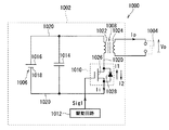
図1は、第1実施形態のパルス放電発生装置の回路図である。 FIG. 1 is a circuit diagram of the pulse discharge generator of the first embodiment.
図1に示すように、パルス放電発生装置1000は、パルス発生回路1002と、放電体1004と、を備える。パルス発生回路1002が発生したパルス電圧は放電体1004に印加され、放電体1004にはパルス放電が発生する。これにより、放電体1004においてプラズマが発生する。パルス放電発生装置1000がプラズマの発生以外の用途に用いられてもよい。
As shown in FIG. 1, the
放電体1004は、対向する電極の容量性の負荷である。パルス放電発生装置1000においては、放電体1004にパルス電圧が印加されパルス発生回路1002から放電体1004へ電流が流れると、放電体1004からパルス発生回路1002へ電流が還流するキックバックが発生する。
The
(パルス発生回路)
パルス発生回路1002は、直流源1006と、トランス1008と、MOSFET(酸化金属被膜電界効果トランジスタ)1010と、駆動回路1012と、キャパシタ1014と、を備える。パルス発生回路1002は、誘導性素子に蓄積された誘導エネルギーを短時間で放出する誘導エネルギー蓄積型の電源である。
(Pulse generation circuit)
The
バッテリ等からなる直流源1006は、正極1016と負極1018との間に直流電圧を発生する。直流源1006の正極1016から負極1018へ至る導通経路1020には、トランス1008の1次側巻線1022と、MOSFET1010のドレイン−ソース間とが挿入される。トランス1008の1次側巻線1022の一端は直流源1006の正極1016に接続され、トランス1008の1次側巻線1022の他端はMOSFET1010のドレインに接続され、MOSFET1010のソースは直流源1006の負極1018に接続される。トランス1008の2次側巻線1024からはパルス電圧が出力され、トランス1008の2次側巻線1024に並列に接続された放電体1004にはパルス発生回路1002から出力されたパルス電圧が印加される。キャパシタ1014は、直流源1006に並列に接続される。誘導性素子がトランス1008であることは必須ではなく、トランス1008の1次側巻線1022が挿入されている位置にインダクタが挿入され、インダクタの両端からパルス電圧が出力されてもよい。
A
MOSFET1010のドレイン−ソース間には、MOSFET1010のゲートに入力された駆動信号Sig1に応じて導通状態が変化するチャネル1026がある。チャネル1026には寄生ダイオード1028が寄生する。MOSFET1010のドレイン−ソース間は、寄生ダイオード1028を経由して直流源1006の負極1018から正極1016へ流れる電流が寄生ダイオード1028の順方向電流となるように導通経路1020に挿入される。寄生ダイオード1028は、「保護ダイオード」、「ボディダイオード」、「内部逆接続ダイオード」、「フライホイールダイオード」等とも呼ばれる。
Between the drain and source of the
MOSFET1010のゲートには駆動回路1012から駆動信号Sig1が入力される。駆動信号Sig1は、MOSFET1010のチャネル1026を導通させるオン期間とチャネル1026を導通させないオフ期間とを交互に繰り返す。
A drive signal Sig 1 is input from the
パルス発生回路1002においては、チャネル1026が導通した状態から導通していない状態へ変化すると、導通経路1020を流れる電流Iiが遮断され、トランス1008の2次側巻線1024に相互誘導によりパルス電圧が出力される。以下では、このパルス電圧を「主パルス電圧」という。
In the
また、パルス発生回路1002においては、オフ期間に寄生ダイオード1028が順方向にバイアスされると、直流源1006の負極1018から正極1016へ向かう電流I1が寄生ダイオード1028を経由して導通経路1020を流れる。電流I1が流れなくなった直後も、寄生ダイオード1028は逆導通しており、直流源1006の正極1016から負極1018へ向かう電流I2が寄生ダイオード1028を経由して導通経路1020を流れる。寄生ダイオード1028が逆回復すると、電流I2は流れなくなる。したがって、寄生ダイオード1028が順方向にバイアスされると、チャネル1026が導通した状態から導通していない状態へ変化したときと同じように導通経路1020を流れる電流Iiが変化し、トランス1008の2次側巻線1024にパルス電圧が出力される。以下では、このパルス電圧を「付随パルス電圧」という。
In the
一方、先述したように、パルス放電発生装置1000においては、放電体1004にパルス電圧が印加された後に、放電体1004からパルス発生回路1002へ電流が還流するキックバックが発生し、寄生ダイオード1028が順方向にバイアスされる。
On the other hand, as described above, in the
これらのことから、パルス放電発生装置1000においては、主パルスが発生すると付随パルスが誘起され、付随パルスが発生すると次の付随パルスが誘起される。したがって、パルス放電発生装置1000においては、主パルスが発生すると付随パルスが繰り返し発生する。そこで、パルス放電発生装置1000においては、オフ期間に1回以上の付随パルス電圧が発生するようにオフ期間の長さが設定される。これにより、オフ期間に2回以上のパルス電圧が発生し、発生するパルス電圧の繰り返し周波数がスイッチング素子のスイッチング周波数より高くなり、効率を著しく低下させることなく繰り返し周波数が高いパルス電圧を発生できる。
For these reasons, in the
(パルス放電発生装置の動作)
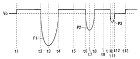
図2から図5までは、それぞれ、駆動信号Sig1、導通経路1020を流れる電流Ii、パルス発生回路1002から放電体1004へ流れる電流Io、放電体1004に印加される電圧(パルス発生回路1002が出力する電圧)Voのタイミングt1からt13までの一周期の時間変化を示す。
(Operation of pulse discharge generator)
2 to 5, respectively, the drive signal Sig1, the current Ii flowing through the
タイミングt1からt2までのオン期間には、図2に示すように、オン信号がMOSFET1010のゲートに入力され、チャネル1026が導通し、導通経路1020が閉じられる。オン期間には、図3に示すように、電流Iiが正方向に増加し、トランス1008に誘導エネルギーが蓄積される。
In the ON period from timing t1 to t2, as shown in FIG. 2, an ON signal is input to the gate of the
タイミングt2からタイミングt13までのオフ期間には、図2に示すように、オフ信号がMOSFET1010のゲートに入力され、チャネル1026が導通せず、導通経路1020が開かれる。オフ期間には、トランス1008に蓄積された誘導エネルギーが放出され、図5に示すように、最初に主パルス電圧P1が発生し、続いて付随パルス電圧P2及びP3が発生する。図5には、付随パルス電圧が発生する回数が2回である場合が示されるが、付随パルス電圧が発生する回数は1回であってもよく3回以上であってもよい。付随パルス電圧が発生する回数は、オフ期間の長さ、寄生ダイオード1028の逆回復特性等によって決まる。
In an off period from timing t2 to timing t13, as shown in FIG. 2, an off signal is input to the gate of the
チャネル1026が導通した状態から導通していない状態へ変化するタイミングt2には、図4に示すように、電流Ioが負方向に急激に上昇してから下降し始め、図5に示すように、電圧Voが負方向に急激に上昇し始め、主パルス電圧P1の発生が始まる。
At the timing t2 when the
タイミングt3には、図4に示すように、主パルス電圧P1が印加された放電体1004からの電流の還流により電流Ioが負方向から正方向へ反転し正方向へ上昇し始め、図5に示すように、電圧Voがピークに達し下降し始める。
At timing t3, as shown in FIG. 4, the current Io reverses from the negative direction to the positive direction due to the return of the current from the
タイミングt4には、寄生ダイオード1028が順方向にバイアスされ、図3に示すように、電流Iiが負方向に急激に上昇してから下降し始め、図4に示すように、電流Ioが急激に下降し、図5に示すように、電圧Voが急激に下降し、主パルス電圧P1の発生が終わる。
At the timing t4, the
タイミングt5には、主パルス電圧P1が印加された放電体1004からの電流の還流により寄生ダイオード1028が逆導通し、図3に示すように、電流Iiが負方向から正方向に反転し正方向へ増加し始める。
At timing t5, the
タイミングt6には、寄生ダイオード1028が逆回復し、図3に示すように、電流Iiが急激に下降し、図4に示すように、電流Ioが負方向に急激に上昇してから下降し始め、図5に示すように、電圧Voが負方向に急激に上昇し始め、1回目の付随パルス電圧P2の発生が始まる。
At timing t6, the
タイミングt7には、図4に示すように、1回目の付随パルス電圧P2が印加された放電体1004からの電流の還流により電流Ioが負方向から正方向へ反転し正方向へ上昇し始め、図5に示すように、電圧Voがピークに達し下降し始める。
At timing t7, as shown in FIG. 4, the current Io reverses from the negative direction to the positive direction and starts to rise in the positive direction due to the return of the current from the
タイミングt8においては、寄生ダイオード1028が順方向にバイアスされ、図3に示すように、電流Iiが負方向に急激に上昇してから下降し始め、図4に示すように、電流Ioが急激に下降し、図5に示すように、電圧Voが急激に下降し、1回目の付随パルス電圧P2の発生が終わる。
At timing t8, the
タイミングt9には、1回目の付随パルス電圧P2が印加された放電体1004からの電流の還流により寄生ダイオード1028が逆導通し、図3に示すように、電流Iiが負方向から正方向に反転し正方向へ増加し始める。
At timing t9, the
タイミングt10には、寄生ダイオード1028が逆回復し、図3に示すように、電流Iiが急激に下降し、図4に示すように、電流Ioが負方向に急激に上昇してから下降し始め、図5に示すように、電圧Voが負方向に急激に上昇し始め、2回目の付随パルス電圧P3の発生が始まる。
At timing t10, the
タイミングt11には、図4に示すように、2回目の付随パルス電圧P3が印加された放電体1004からの電流の還流により電流Ioが負方向から正方向へ反転し正方向へ上昇し始め、図5に示すように、電圧Voがピークに達し下降し始める。
At timing t11, as shown in FIG. 4, the current Io reverses from the negative direction to the positive direction and starts to rise in the positive direction due to the return of the current from the
タイミングt12には、寄生ダイオード1028が順方向にバイアスされ、図4に示すように、電流Ioが急激に下降し、図5に示すように、電圧Voが急激に下降し、2回目の付随パルス電圧P3の発生が終わる。
At the timing t12, the
オフ期間の長さは、タイミングt2から、主パルス電圧又は付随パルス電圧が印加された放電体1004から還流する電流により逆導通した寄生ダイオード1028が逆回復したときに発生する付随パルス電圧の発生が終わるタイミングt8,t12等までの時間より長く設定される。これにより、オフ期間に2回以上のパルス電圧が発生する。パルス電圧が発生する回数は、オフ期間の長さにより調整される。
The length of the off-period is the generation of the accompanying pulse voltage that occurs when the
{第2実施形態}
(パルス放電発生装置の概略)
第2実施形態は、パルス放電発生装置に関する。
{Second Embodiment}
(Outline of pulse discharge generator)
The second embodiment relates to a pulse discharge generator.
図6は、第2実施形態のパルス発生装置の回路図である。 FIG. 6 is a circuit diagram of the pulse generator of the second embodiment.
図6に示すように、パルス放電発生装置2000は、第1実施形態のパルス放電発生装置1000と同じように、パルス発生回路2002と、放電体2004と、を備える。パルス発生回路2002は、第1実施形態のパルス発生回路1002と同じように、直流源2006と、トランス2008と、MOSFET2010と、駆動回路2012と、キャパシタ2014と、を備える。パルス発生回路2002は、誘導性素子に蓄積された誘導エネルギーを短時間で放出する誘導エネルギー蓄積型の電源である。直流源2006は、正極2016と負極2018との間に直流電圧を発生する。直流源2006の正極2016から負極2018へ至る導通経路2020には、トランス2008の1次側巻線2022と、MOSFET2010のドレイン−ソース間とが挿入される。トランス2008の2次側巻線2024からはパルス電圧が出力される。
As shown in FIG. 6, the
パルス放電発生装置1000とパルス発生装置2000との違いは、パルス発生装置2000においては、外付けダイオード2100がさらに設けられることにある。外付けダイオード2100は、外付けダイオード2100を経由して直流電源の負極1018から正極1016へ流れる電流が順方向電流となるようにチャネル2026に並列に接続される。外付けダイオード2100のアノードはMOSFET2010のソースに接続され、外付けダイオード2100のカソードはMOSFET2010のドレインに接続される。
The difference between the
パルス放電発生装置2000は、パルス放電発生装置1000と同じように動作するが、付随パルス電圧P2及びP3の発生が始まるタイミングt6及びt10は、パルス電圧が印加された放電体2004から帰還する電流により逆導通した寄生ダイオード2028及び外付けダイオード2100が逆回復したときである。また、オフ期間の長さは、タイミングt2から、主パルス電圧又は付随パルス電圧が印加された放電体2004から還流する電流により逆導通した寄生ダイオード2028及び外付けダイオード2100が逆回復したときに発生する付随パルス電圧P2及びP3の発生が終わるタイミングt8,t12等までの時間より長く設定される。
The
パルス放電発生装置2000においては、オフ期間に2回以上のパルス電圧が発生し、発生するパルス電圧の繰り返し周波数がスイッチング素子のスイッチング周波数より高くなり、効率を著しく低下させることなく繰り返し周波数が高いパルス電圧を発生できることに加えて、外付けダイオード2100により、逆回復特性が適切に設定される。
In the
本発明は詳細に示され記述されたが、上記の記述は全ての局面において例示であって限定的ではない。しがって、本発明の範囲からはずれることなく無数の修正及び変形が案出されうると解される。 While the invention has been shown and described in detail, the above description is illustrative in all aspects and not restrictive. Thus, it will be appreciated that numerous modifications and variations can be devised without departing from the scope of the invention.
1000,2000 パルス放電発生装置
1002,2002 パルス発生回路
1004,2004 放電体
1006,2006 直流源
1008,2008 トランス
1010,2010 MOSFET
1012,2012 駆動回路
1020,2020 導通経路
1026,2026 チャネル
1028,2028 寄生ダイオード
2100 外付けダイオード
1000, 2000
1012, 2012
Claims (2)
パルス電圧を発生する誘導エネルギー蓄積型のパルス発生回路と、
前記パルス発生回路が発生したパルス電圧が印加される容量性の負荷と、
を備え、
前記パルス発生回路は、
正極と負極との間に直流電圧を発生する直流源と、
前記正極から前記負極へ至る導通経路と、
前記導通経路に挿入される誘導性素子と、
入力された駆動信号に応じて導通状態が変化するチャネルを備え、前記チャネルに寄生ダイオードが寄生しており、前記寄生ダイオードを経由して前記負極から前記正極へ流れる電流が前記寄生ダイオードの順方向電流となるように前記導通経路に挿入されるユニポーラ型のスイッチング素子と、
前記チャネルを導通させるオン期間と前記チャネルを導通させないオフ期間とを交互に繰り返す駆動信号を前記スイッチング素子に入力する駆動回路と、
を備え、
前記オフ期間の長さが、
前記チャネルが導通した状態から導通していない状態へ変化したときに発生する主パルス電圧の発生が始まる第1のタイミングから、
パルス電圧が印加された前記負荷から帰還する電流により逆導通した前記寄生ダイオードが逆回復したときに発生する付随パルス電圧の発生が終わる第2のタイミングまで、
の時間より長く設定される
パルス放電発生装置。 A pulse discharge generator,
An inductive energy storage type pulse generation circuit for generating a pulse voltage;
A capacitive load to which the pulse voltage generated by the pulse generation circuit is applied;
With
The pulse generation circuit includes:
A DC source that generates a DC voltage between the positive electrode and the negative electrode;
A conduction path from the positive electrode to the negative electrode;
An inductive element inserted into the conduction path;
A channel whose conduction state changes according to an input drive signal, and a parasitic diode is parasitic on the channel, and a current flowing from the negative electrode to the positive electrode via the parasitic diode is forward direction of the parasitic diode. A unipolar switching element inserted into the conduction path so as to become an electric current;
A drive circuit for inputting a drive signal to the switching element that alternately repeats an on period for conducting the channel and an off period for not conducting the channel;
With
The length of the off period is
From the first timing when the generation of the main pulse voltage that occurs when the channel changes from a conductive state to a non-conductive state,
Until the second timing when generation of the accompanying pulse voltage that occurs when the parasitic diode reversely turned on by the current fed back from the load to which the pulse voltage is applied is reversely recovered ends,
Pulse discharge generator set longer than the time.
パルス電圧を発生する誘導エネルギー蓄積型のパルス発生回路と、
前記パルス発生回路が発生したパルス電圧が印加される容量性の負荷と、
を備え、
前記パルス発生回路は、
正極と負極との間に直流電圧を発生する直流源と、
前記正極から前記負極へ至る導通経路と、
前記導通経路に挿入される誘導性素子と、
入力された駆動信号に応じて導通状態が変化するチャネルを備え、前記チャネルに寄生ダイオードが寄生しており、前記寄生ダイオードを経由して前記負極から前記正極へ流れる電流が前記寄生ダイオードの順方向電流となるように前記導通経路に挿入されるユニポーラ型のスイッチング素子と、
前記チャネルを導通させるオン期間と前記チャネルを導通させないオフ期間とを交互に繰り返す駆動信号を前記スイッチング素子に入力する駆動回路と、
前記チャネルに並列に接続される外付けダイオードと、
を備え、
前記外付けダイオードは、前記外付けダイオードを経由して前記負極から前記正極へ流れる電流が順方向電流となるように前記チャネルに並列に接続され、
前記オフ期間の長さが、
前記チャネルが導通した状態から導通していない状態へ変化したときに発生する主パルス電圧の発生が始まる第1のタイミングから、
パルス電圧が印加された前記負荷から帰還する電流により逆導通した前記寄生ダイオード及び前記外付けダイオードが逆回復したときに発生する付随パルス電圧の発生が終わる第2のタイミングまで、
の時間より長く設定される
パルス放電発生装置。 A pulse discharge generator,
An inductive energy storage type pulse generation circuit for generating a pulse voltage;
A capacitive load to which the pulse voltage generated by the pulse generation circuit is applied;
With
The pulse generation circuit includes:
A DC source that generates a DC voltage between the positive electrode and the negative electrode;
A conduction path from the positive electrode to the negative electrode;
An inductive element inserted into the conduction path;
A channel whose conduction state changes according to an input drive signal, and a parasitic diode is parasitic on the channel, and a current flowing from the negative electrode to the positive electrode via the parasitic diode is forward direction of the parasitic diode. A unipolar switching element inserted into the conduction path so as to become an electric current;
A drive circuit for inputting a drive signal to the switching element that alternately repeats an on period for conducting the channel and an off period for not conducting the channel;
An external diode connected in parallel to the channel;
With
The external diode is connected in parallel to the channel so that a current flowing from the negative electrode to the positive electrode via the external diode becomes a forward current,
The length of the off period is
From the first timing when the generation of the main pulse voltage that occurs when the channel changes from a conductive state to a non-conductive state,
Until the second timing when generation of the accompanying pulse voltage that occurs when the parasitic diode and the external diode reversely conducted by the current fed back from the load to which the pulse voltage is applied is reversely recovered ends,
Pulse discharge generator set longer than the time.
Priority Applications (1)
| Application Number | Priority Date | Filing Date | Title |
|---|---|---|---|
| JP2010269146A JP2012120017A (en) | 2010-12-02 | 2010-12-02 | Pulse discharge generation device |
Applications Claiming Priority (1)
| Application Number | Priority Date | Filing Date | Title |
|---|---|---|---|
| JP2010269146A JP2012120017A (en) | 2010-12-02 | 2010-12-02 | Pulse discharge generation device |
Publications (1)
| Publication Number | Publication Date |
|---|---|
| JP2012120017A true JP2012120017A (en) | 2012-06-21 |
Family
ID=46502351
Family Applications (1)
| Application Number | Title | Priority Date | Filing Date |
|---|---|---|---|
| JP2010269146A Pending JP2012120017A (en) | 2010-12-02 | 2010-12-02 | Pulse discharge generation device |
Country Status (1)
| Country | Link |
|---|---|
| JP (1) | JP2012120017A (en) |
-
2010
- 2010-12-02 JP JP2010269146A patent/JP2012120017A/en active Pending
Similar Documents
| Publication | Publication Date | Title |
|---|---|---|
| US8743565B2 (en) | High power converter architecture | |
| US9019724B2 (en) | High power converter architecture | |
| US20140254208A1 (en) | Auxiliary Resonant Apparatus for LLC Converters | |
| US7535733B2 (en) | Method of controlling DC-to-DC converter whereby switching control sequence applied to switching elements suppresses voltage surges at timings of switch-off of switching elements | |
| JP2015159710A (en) | energy recovery snubber | |
| JP6840032B2 (en) | Insulated switching power supply | |
| JP2015186363A (en) | DC-DC converter | |
| JP2012119961A (en) | Pulse generation circuit | |
| Chennu et al. | Study on Resonant Gate Driver circuits for high frequency applications | |
| Dutta et al. | A soft-switched flyback converter with recovery of stored energy in leakage inductance | |
| JP5761351B2 (en) | Snubber circuit | |
| JP5472354B2 (en) | Switching power supply | |
| JP2014150654A (en) | Gate Drive circuit | |
| US20170244400A1 (en) | Pulse modulator | |
| CN107154727B (en) | Active absorption self-driving circuit | |
| JP2012120017A (en) | Pulse discharge generation device | |
| WO2013174152A1 (en) | Synchronous rectification device and synchronous rectification power supply | |
| JP6942040B2 (en) | Insulated switching power supply | |
| TWI465020B (en) | Can produce three times the input voltage of the gate driver and drive method | |
| RU2637813C1 (en) | Quasi-resonant voltage converter with high coefficient of efficiency | |
| RU2581600C1 (en) | Two-stroke flyback dc-to-dc converter | |
| Reshetnikov et al. | Power supply for driver | |
| JP6945429B2 (en) | Insulated switching power supply | |
| Kar et al. | Design, fabrication, simulation and testing of a phase modulated resonant transition converter | |
| TW201336218A (en) | Power conversion device |