JP2012109307A - Semiconductor device, and method of manufacturing semiconductor device - Google Patents
Semiconductor device, and method of manufacturing semiconductor device Download PDFInfo
- Publication number
- JP2012109307A JP2012109307A JP2010255088A JP2010255088A JP2012109307A JP 2012109307 A JP2012109307 A JP 2012109307A JP 2010255088 A JP2010255088 A JP 2010255088A JP 2010255088 A JP2010255088 A JP 2010255088A JP 2012109307 A JP2012109307 A JP 2012109307A
- Authority
- JP
- Japan
- Prior art keywords
- semiconductor device
- semiconductor chip
- wiring board
- shield layer
- magnetic shield
- Prior art date
- Legal status (The legal status is an assumption and is not a legal conclusion. Google has not performed a legal analysis and makes no representation as to the accuracy of the status listed.)
- Pending
Links
Images


Classifications
-
- H—ELECTRICITY
- H01—ELECTRIC ELEMENTS
- H01L—SEMICONDUCTOR DEVICES NOT COVERED BY CLASS H10
- H01L23/00—Details of semiconductor or other solid state devices
- H01L23/58—Structural electrical arrangements for semiconductor devices not otherwise provided for, e.g. in combination with batteries
-
- H—ELECTRICITY
- H01—ELECTRIC ELEMENTS
- H01L—SEMICONDUCTOR DEVICES NOT COVERED BY CLASS H10
- H01L23/00—Details of semiconductor or other solid state devices
- H01L23/12—Mountings, e.g. non-detachable insulating substrates
- H01L23/13—Mountings, e.g. non-detachable insulating substrates characterised by the shape
-
- H—ELECTRICITY
- H01—ELECTRIC ELEMENTS
- H01L—SEMICONDUCTOR DEVICES NOT COVERED BY CLASS H10
- H01L23/00—Details of semiconductor or other solid state devices
- H01L23/552—Protection against radiation, e.g. light or electromagnetic waves
-
- H—ELECTRICITY
- H01—ELECTRIC ELEMENTS
- H01L—SEMICONDUCTOR DEVICES NOT COVERED BY CLASS H10
- H01L24/00—Arrangements for connecting or disconnecting semiconductor or solid-state bodies; Methods or apparatus related thereto
- H01L24/01—Means for bonding being attached to, or being formed on, the surface to be connected, e.g. chip-to-package, die-attach, "first-level" interconnects; Manufacturing methods related thereto
- H01L24/26—Layer connectors, e.g. plate connectors, solder or adhesive layers; Manufacturing methods related thereto
- H01L24/28—Structure, shape, material or disposition of the layer connectors prior to the connecting process
- H01L24/29—Structure, shape, material or disposition of the layer connectors prior to the connecting process of an individual layer connector
-
- H—ELECTRICITY
- H01—ELECTRIC ELEMENTS
- H01L—SEMICONDUCTOR DEVICES NOT COVERED BY CLASS H10
- H01L24/00—Arrangements for connecting or disconnecting semiconductor or solid-state bodies; Methods or apparatus related thereto
- H01L24/01—Means for bonding being attached to, or being formed on, the surface to be connected, e.g. chip-to-package, die-attach, "first-level" interconnects; Manufacturing methods related thereto
- H01L24/26—Layer connectors, e.g. plate connectors, solder or adhesive layers; Manufacturing methods related thereto
- H01L24/31—Structure, shape, material or disposition of the layer connectors after the connecting process
- H01L24/32—Structure, shape, material or disposition of the layer connectors after the connecting process of an individual layer connector
-
- H—ELECTRICITY
- H10—SEMICONDUCTOR DEVICES; ELECTRIC SOLID-STATE DEVICES NOT OTHERWISE PROVIDED FOR
- H10B—ELECTRONIC MEMORY DEVICES
- H10B61/00—Magnetic memory devices, e.g. magnetoresistive RAM [MRAM] devices
- H10B61/10—Magnetic memory devices, e.g. magnetoresistive RAM [MRAM] devices comprising components having two electrodes, e.g. diodes or MIM elements
-
- H—ELECTRICITY
- H01—ELECTRIC ELEMENTS
- H01L—SEMICONDUCTOR DEVICES NOT COVERED BY CLASS H10
- H01L2223/00—Details relating to semiconductor or other solid state devices covered by the group H01L23/00
- H01L2223/544—Marks applied to semiconductor devices or parts
- H01L2223/54426—Marks applied to semiconductor devices or parts for alignment
-
- H—ELECTRICITY
- H01—ELECTRIC ELEMENTS
- H01L—SEMICONDUCTOR DEVICES NOT COVERED BY CLASS H10
- H01L2224/00—Indexing scheme for arrangements for connecting or disconnecting semiconductor or solid-state bodies and methods related thereto as covered by H01L24/00
- H01L2224/01—Means for bonding being attached to, or being formed on, the surface to be connected, e.g. chip-to-package, die-attach, "first-level" interconnects; Manufacturing methods related thereto
- H01L2224/02—Bonding areas; Manufacturing methods related thereto
- H01L2224/04—Structure, shape, material or disposition of the bonding areas prior to the connecting process
- H01L2224/0401—Bonding areas specifically adapted for bump connectors, e.g. under bump metallisation [UBM]
-
- H—ELECTRICITY
- H01—ELECTRIC ELEMENTS
- H01L—SEMICONDUCTOR DEVICES NOT COVERED BY CLASS H10
- H01L2224/00—Indexing scheme for arrangements for connecting or disconnecting semiconductor or solid-state bodies and methods related thereto as covered by H01L24/00
- H01L2224/01—Means for bonding being attached to, or being formed on, the surface to be connected, e.g. chip-to-package, die-attach, "first-level" interconnects; Manufacturing methods related thereto
- H01L2224/10—Bump connectors; Manufacturing methods related thereto
- H01L2224/15—Structure, shape, material or disposition of the bump connectors after the connecting process
- H01L2224/16—Structure, shape, material or disposition of the bump connectors after the connecting process of an individual bump connector
- H01L2224/161—Disposition
- H01L2224/16151—Disposition the bump connector connecting between a semiconductor or solid-state body and an item not being a semiconductor or solid-state body, e.g. chip-to-substrate, chip-to-passive
- H01L2224/16221—Disposition the bump connector connecting between a semiconductor or solid-state body and an item not being a semiconductor or solid-state body, e.g. chip-to-substrate, chip-to-passive the body and the item being stacked
- H01L2224/16225—Disposition the bump connector connecting between a semiconductor or solid-state body and an item not being a semiconductor or solid-state body, e.g. chip-to-substrate, chip-to-passive the body and the item being stacked the item being non-metallic, e.g. insulating substrate with or without metallisation
-
- H—ELECTRICITY
- H01—ELECTRIC ELEMENTS
- H01L—SEMICONDUCTOR DEVICES NOT COVERED BY CLASS H10
- H01L2224/00—Indexing scheme for arrangements for connecting or disconnecting semiconductor or solid-state bodies and methods related thereto as covered by H01L24/00
- H01L2224/01—Means for bonding being attached to, or being formed on, the surface to be connected, e.g. chip-to-package, die-attach, "first-level" interconnects; Manufacturing methods related thereto
- H01L2224/26—Layer connectors, e.g. plate connectors, solder or adhesive layers; Manufacturing methods related thereto
- H01L2224/28—Structure, shape, material or disposition of the layer connectors prior to the connecting process
- H01L2224/29—Structure, shape, material or disposition of the layer connectors prior to the connecting process of an individual layer connector
- H01L2224/29001—Core members of the layer connector
- H01L2224/29099—Material
- H01L2224/291—Material with a principal constituent of the material being a metal or a metalloid, e.g. boron [B], silicon [Si], germanium [Ge], arsenic [As], antimony [Sb], tellurium [Te] and polonium [Po], and alloys thereof
- H01L2224/29101—Material with a principal constituent of the material being a metal or a metalloid, e.g. boron [B], silicon [Si], germanium [Ge], arsenic [As], antimony [Sb], tellurium [Te] and polonium [Po], and alloys thereof the principal constituent melting at a temperature of less than 400°C
-
- H—ELECTRICITY
- H01—ELECTRIC ELEMENTS
- H01L—SEMICONDUCTOR DEVICES NOT COVERED BY CLASS H10
- H01L2224/00—Indexing scheme for arrangements for connecting or disconnecting semiconductor or solid-state bodies and methods related thereto as covered by H01L24/00
- H01L2224/01—Means for bonding being attached to, or being formed on, the surface to be connected, e.g. chip-to-package, die-attach, "first-level" interconnects; Manufacturing methods related thereto
- H01L2224/26—Layer connectors, e.g. plate connectors, solder or adhesive layers; Manufacturing methods related thereto
- H01L2224/28—Structure, shape, material or disposition of the layer connectors prior to the connecting process
- H01L2224/29—Structure, shape, material or disposition of the layer connectors prior to the connecting process of an individual layer connector
- H01L2224/29001—Core members of the layer connector
- H01L2224/29099—Material
- H01L2224/291—Material with a principal constituent of the material being a metal or a metalloid, e.g. boron [B], silicon [Si], germanium [Ge], arsenic [As], antimony [Sb], tellurium [Te] and polonium [Po], and alloys thereof
- H01L2224/29138—Material with a principal constituent of the material being a metal or a metalloid, e.g. boron [B], silicon [Si], germanium [Ge], arsenic [As], antimony [Sb], tellurium [Te] and polonium [Po], and alloys thereof the principal constituent melting at a temperature of greater than or equal to 950°C and less than 1550°C
- H01L2224/2916—Iron [Fe] as principal constituent
-
- H—ELECTRICITY
- H01—ELECTRIC ELEMENTS
- H01L—SEMICONDUCTOR DEVICES NOT COVERED BY CLASS H10
- H01L2224/00—Indexing scheme for arrangements for connecting or disconnecting semiconductor or solid-state bodies and methods related thereto as covered by H01L24/00
- H01L2224/01—Means for bonding being attached to, or being formed on, the surface to be connected, e.g. chip-to-package, die-attach, "first-level" interconnects; Manufacturing methods related thereto
- H01L2224/26—Layer connectors, e.g. plate connectors, solder or adhesive layers; Manufacturing methods related thereto
- H01L2224/28—Structure, shape, material or disposition of the layer connectors prior to the connecting process
- H01L2224/29—Structure, shape, material or disposition of the layer connectors prior to the connecting process of an individual layer connector
- H01L2224/29001—Core members of the layer connector
- H01L2224/29099—Material
- H01L2224/2919—Material with a principal constituent of the material being a polymer, e.g. polyester, phenolic based polymer, epoxy
-
- H—ELECTRICITY
- H01—ELECTRIC ELEMENTS
- H01L—SEMICONDUCTOR DEVICES NOT COVERED BY CLASS H10
- H01L2224/00—Indexing scheme for arrangements for connecting or disconnecting semiconductor or solid-state bodies and methods related thereto as covered by H01L24/00
- H01L2224/93—Batch processes
- H01L2224/95—Batch processes at chip-level, i.e. with connecting carried out on a plurality of singulated devices, i.e. on diced chips
- H01L2224/97—Batch processes at chip-level, i.e. with connecting carried out on a plurality of singulated devices, i.e. on diced chips the devices being connected to a common substrate, e.g. interposer, said common substrate being separable into individual assemblies after connecting
-
- H—ELECTRICITY
- H01—ELECTRIC ELEMENTS
- H01L—SEMICONDUCTOR DEVICES NOT COVERED BY CLASS H10
- H01L23/00—Details of semiconductor or other solid state devices
- H01L23/28—Encapsulations, e.g. encapsulating layers, coatings, e.g. for protection
- H01L23/31—Encapsulations, e.g. encapsulating layers, coatings, e.g. for protection characterised by the arrangement or shape
- H01L23/3107—Encapsulations, e.g. encapsulating layers, coatings, e.g. for protection characterised by the arrangement or shape the device being completely enclosed
- H01L23/3121—Encapsulations, e.g. encapsulating layers, coatings, e.g. for protection characterised by the arrangement or shape the device being completely enclosed a substrate forming part of the encapsulation
- H01L23/3128—Encapsulations, e.g. encapsulating layers, coatings, e.g. for protection characterised by the arrangement or shape the device being completely enclosed a substrate forming part of the encapsulation the substrate having spherical bumps for external connection
-
- H—ELECTRICITY
- H01—ELECTRIC ELEMENTS
- H01L—SEMICONDUCTOR DEVICES NOT COVERED BY CLASS H10
- H01L23/00—Details of semiconductor or other solid state devices
- H01L23/48—Arrangements for conducting electric current to or from the solid state body in operation, e.g. leads, terminal arrangements ; Selection of materials therefor
- H01L23/488—Arrangements for conducting electric current to or from the solid state body in operation, e.g. leads, terminal arrangements ; Selection of materials therefor consisting of soldered or bonded constructions
- H01L23/498—Leads, i.e. metallisations or lead-frames on insulating substrates, e.g. chip carriers
- H01L23/49811—Additional leads joined to the metallisation on the insulating substrate, e.g. pins, bumps, wires, flat leads
- H01L23/49816—Spherical bumps on the substrate for external connection, e.g. ball grid arrays [BGA]
-
- H—ELECTRICITY
- H01—ELECTRIC ELEMENTS
- H01L—SEMICONDUCTOR DEVICES NOT COVERED BY CLASS H10
- H01L24/00—Arrangements for connecting or disconnecting semiconductor or solid-state bodies; Methods or apparatus related thereto
- H01L24/01—Means for bonding being attached to, or being formed on, the surface to be connected, e.g. chip-to-package, die-attach, "first-level" interconnects; Manufacturing methods related thereto
- H01L24/02—Bonding areas ; Manufacturing methods related thereto
- H01L24/04—Structure, shape, material or disposition of the bonding areas prior to the connecting process
- H01L24/05—Structure, shape, material or disposition of the bonding areas prior to the connecting process of an individual bonding area
-
- H—ELECTRICITY
- H01—ELECTRIC ELEMENTS
- H01L—SEMICONDUCTOR DEVICES NOT COVERED BY CLASS H10
- H01L24/00—Arrangements for connecting or disconnecting semiconductor or solid-state bodies; Methods or apparatus related thereto
- H01L24/01—Means for bonding being attached to, or being formed on, the surface to be connected, e.g. chip-to-package, die-attach, "first-level" interconnects; Manufacturing methods related thereto
- H01L24/10—Bump connectors ; Manufacturing methods related thereto
- H01L24/15—Structure, shape, material or disposition of the bump connectors after the connecting process
- H01L24/16—Structure, shape, material or disposition of the bump connectors after the connecting process of an individual bump connector
-
- H—ELECTRICITY
- H01—ELECTRIC ELEMENTS
- H01L—SEMICONDUCTOR DEVICES NOT COVERED BY CLASS H10
- H01L24/00—Arrangements for connecting or disconnecting semiconductor or solid-state bodies; Methods or apparatus related thereto
- H01L24/93—Batch processes
- H01L24/95—Batch processes at chip-level, i.e. with connecting carried out on a plurality of singulated devices, i.e. on diced chips
- H01L24/97—Batch processes at chip-level, i.e. with connecting carried out on a plurality of singulated devices, i.e. on diced chips the devices being connected to a common substrate, e.g. interposer, said common substrate being separable into individual assemblies after connecting
-
- H—ELECTRICITY
- H01—ELECTRIC ELEMENTS
- H01L—SEMICONDUCTOR DEVICES NOT COVERED BY CLASS H10
- H01L2924/00—Indexing scheme for arrangements or methods for connecting or disconnecting semiconductor or solid-state bodies as covered by H01L24/00
- H01L2924/01—Chemical elements
- H01L2924/01005—Boron [B]
-
- H—ELECTRICITY
- H01—ELECTRIC ELEMENTS
- H01L—SEMICONDUCTOR DEVICES NOT COVERED BY CLASS H10
- H01L2924/00—Indexing scheme for arrangements or methods for connecting or disconnecting semiconductor or solid-state bodies as covered by H01L24/00
- H01L2924/01—Chemical elements
- H01L2924/01006—Carbon [C]
-
- H—ELECTRICITY
- H01—ELECTRIC ELEMENTS
- H01L—SEMICONDUCTOR DEVICES NOT COVERED BY CLASS H10
- H01L2924/00—Indexing scheme for arrangements or methods for connecting or disconnecting semiconductor or solid-state bodies as covered by H01L24/00
- H01L2924/01—Chemical elements
- H01L2924/01029—Copper [Cu]
-
- H—ELECTRICITY
- H01—ELECTRIC ELEMENTS
- H01L—SEMICONDUCTOR DEVICES NOT COVERED BY CLASS H10
- H01L2924/00—Indexing scheme for arrangements or methods for connecting or disconnecting semiconductor or solid-state bodies as covered by H01L24/00
- H01L2924/01—Chemical elements
- H01L2924/01033—Arsenic [As]
-
- H—ELECTRICITY
- H01—ELECTRIC ELEMENTS
- H01L—SEMICONDUCTOR DEVICES NOT COVERED BY CLASS H10
- H01L2924/00—Indexing scheme for arrangements or methods for connecting or disconnecting semiconductor or solid-state bodies as covered by H01L24/00
- H01L2924/01—Chemical elements
- H01L2924/01079—Gold [Au]
-
- H—ELECTRICITY
- H01—ELECTRIC ELEMENTS
- H01L—SEMICONDUCTOR DEVICES NOT COVERED BY CLASS H10
- H01L2924/00—Indexing scheme for arrangements or methods for connecting or disconnecting semiconductor or solid-state bodies as covered by H01L24/00
- H01L2924/01—Chemical elements
- H01L2924/01082—Lead [Pb]
-
- H—ELECTRICITY
- H01—ELECTRIC ELEMENTS
- H01L—SEMICONDUCTOR DEVICES NOT COVERED BY CLASS H10
- H01L2924/00—Indexing scheme for arrangements or methods for connecting or disconnecting semiconductor or solid-state bodies as covered by H01L24/00
- H01L2924/013—Alloys
- H01L2924/014—Solder alloys
-
- H—ELECTRICITY
- H01—ELECTRIC ELEMENTS
- H01L—SEMICONDUCTOR DEVICES NOT COVERED BY CLASS H10
- H01L2924/00—Indexing scheme for arrangements or methods for connecting or disconnecting semiconductor or solid-state bodies as covered by H01L24/00
- H01L2924/06—Polymers
- H01L2924/0665—Epoxy resin
-
- H—ELECTRICITY
- H01—ELECTRIC ELEMENTS
- H01L—SEMICONDUCTOR DEVICES NOT COVERED BY CLASS H10
- H01L2924/00—Indexing scheme for arrangements or methods for connecting or disconnecting semiconductor or solid-state bodies as covered by H01L24/00
- H01L2924/10—Details of semiconductor or other solid state devices to be connected
- H01L2924/11—Device type
- H01L2924/12—Passive devices, e.g. 2 terminal devices
- H01L2924/1204—Optical Diode
- H01L2924/12041—LED
-
- H—ELECTRICITY
- H01—ELECTRIC ELEMENTS
- H01L—SEMICONDUCTOR DEVICES NOT COVERED BY CLASS H10
- H01L2924/00—Indexing scheme for arrangements or methods for connecting or disconnecting semiconductor or solid-state bodies as covered by H01L24/00
- H01L2924/10—Details of semiconductor or other solid state devices to be connected
- H01L2924/11—Device type
- H01L2924/14—Integrated circuits
- H01L2924/143—Digital devices
- H01L2924/1434—Memory
- H01L2924/1435—Random access memory [RAM]
-
- H—ELECTRICITY
- H01—ELECTRIC ELEMENTS
- H01L—SEMICONDUCTOR DEVICES NOT COVERED BY CLASS H10
- H01L2924/00—Indexing scheme for arrangements or methods for connecting or disconnecting semiconductor or solid-state bodies as covered by H01L24/00
- H01L2924/15—Details of package parts other than the semiconductor or other solid state devices to be connected
- H01L2924/151—Die mounting substrate
- H01L2924/1515—Shape
- H01L2924/15158—Shape the die mounting substrate being other than a cuboid
- H01L2924/15159—Side view
-
- H—ELECTRICITY
- H01—ELECTRIC ELEMENTS
- H01L—SEMICONDUCTOR DEVICES NOT COVERED BY CLASS H10
- H01L2924/00—Indexing scheme for arrangements or methods for connecting or disconnecting semiconductor or solid-state bodies as covered by H01L24/00
- H01L2924/15—Details of package parts other than the semiconductor or other solid state devices to be connected
- H01L2924/151—Die mounting substrate
- H01L2924/153—Connection portion
- H01L2924/1531—Connection portion the connection portion being formed only on the surface of the substrate opposite to the die mounting surface
- H01L2924/15311—Connection portion the connection portion being formed only on the surface of the substrate opposite to the die mounting surface being a ball array, e.g. BGA
-
- H—ELECTRICITY
- H01—ELECTRIC ELEMENTS
- H01L—SEMICONDUCTOR DEVICES NOT COVERED BY CLASS H10
- H01L2924/00—Indexing scheme for arrangements or methods for connecting or disconnecting semiconductor or solid-state bodies as covered by H01L24/00
- H01L2924/15—Details of package parts other than the semiconductor or other solid state devices to be connected
- H01L2924/181—Encapsulation
- H01L2924/1815—Shape
- H01L2924/1816—Exposing the passive side of the semiconductor or solid-state body
- H01L2924/18161—Exposing the passive side of the semiconductor or solid-state body of a flip chip
Abstract
Description
本発明は、磁気記憶素子を有する半導体装置及び半導体装置の製造方法に関する。 The present invention relates to a semiconductor device having a magnetic memory element and a method for manufacturing the semiconductor device.
記憶素子の一例である磁気記憶素子(MRAM:Magnetoresistive Random Access Memory)を実用化するための開発が進められている。磁気記憶素子は、電子スピンの向きを書き換えることにより情報を書き込む素子である。このため、磁気記憶素子は、外部の静磁場によって情報が誤消去又は誤書込されてしまう可能性がある。これに対して、例えば特許文献1及び2に示すように、磁気記憶素子を有する半導体チップを磁気シールドで覆う構造が検討されている。
Development for putting a magnetic memory element (MRAM: Magnetoresistive Random Access Memory), which is an example of a memory element, into practical use is in progress. A magnetic memory element is an element that writes information by rewriting the direction of electron spin. For this reason, in the magnetic memory element, information may be erroneously erased or erroneously written by an external static magnetic field. On the other hand, for example, as shown in
磁気シールドから半導体チップに向けて磁気が漏れることを抑制するためには、特許文献2のように、半導体チップを直接磁気シールド層で覆うことが望ましい。しかし半導体チップを直接磁気シールド層で覆った場合、半導体チップを配線基板にフリップチップ実装しようとすると、磁気シールド層よりもバンプを高くする必要がある。この場合、バンプを狭いピッチで配置することが難しくなってしまう。 In order to suppress the leakage of magnetism from the magnetic shield toward the semiconductor chip, it is desirable to directly cover the semiconductor chip with a magnetic shield layer as in Patent Document 2. However, when the semiconductor chip is directly covered with the magnetic shield layer, it is necessary to make the bumps higher than the magnetic shield layer when the semiconductor chip is flip-chip mounted on the wiring board. In this case, it becomes difficult to arrange the bumps at a narrow pitch.
本発明によれば、磁気記憶素子を有するとともに、第1面に電極パッドを有する半導体チップと、
少なくとも前記電極パッドが露出した状態で前記半導体チップを被覆する磁気シールド層と、
前記半導体チップがバンプを介して接続された配線基板と、
を備え、
前記半導体チップと前記配線基板は、少なくとも一方が凸部を有しており、当該凸部上に前記バンプが設けられている半導体装置が提供される。
According to the present invention, a semiconductor chip having a magnetic memory element and having an electrode pad on the first surface;
A magnetic shield layer covering the semiconductor chip with at least the electrode pad exposed;
A wiring board to which the semiconductor chip is connected via bumps;
With
At least one of the semiconductor chip and the wiring board has a convex portion, and a semiconductor device is provided in which the bump is provided on the convex portion.
本発明によれば、半導体チップと前記配線基板は、少なくとも一方が凸部を有している。このため、バンプの高さを小さくすることができる。そして、これに伴ってバンプ径を小さくすることができる。従って、バンプを狭いピッチで配置することができる。 According to the present invention, at least one of the semiconductor chip and the wiring board has a convex portion. For this reason, the height of the bump can be reduced. Along with this, the bump diameter can be reduced. Accordingly, the bumps can be arranged at a narrow pitch.
本発明によれば、磁気記憶素子を有するとともに第1面に電極パッドを有する半導体チップを、少なくとも前記電極パッドが露出するように磁気シールド層で被覆する工程と、
前記半導体チップを配線基板にバンプを介して接続する工程と、
を備え、
前記半導体チップと前記配線基板は、少なくとも一方が凸部を有しており、当該凸部上に前記バンプが設けられている半導体装置の製造方法が提供される。
According to the present invention, a step of covering a semiconductor chip having a magnetic memory element and having an electrode pad on the first surface with a magnetic shield layer so that at least the electrode pad is exposed;
Connecting the semiconductor chip to a wiring board via bumps;
With
At least one of the semiconductor chip and the wiring board has a convex portion, and a method of manufacturing a semiconductor device in which the bump is provided on the convex portion is provided.
本発明によれば、半導体チップを磁気シールド層で被覆しても、バンプを狭いピッチで配置することができる。 According to the present invention, even when the semiconductor chip is covered with the magnetic shield layer, the bumps can be arranged at a narrow pitch.
以下、本発明の実施の形態について、図面を用いて説明する。尚、すべての図面において、同様な構成要素には同様の符号を付し、適宜説明を省略する。 Hereinafter, embodiments of the present invention will be described with reference to the drawings. In all the drawings, the same reference numerals are given to the same components, and the description will be omitted as appropriate.
(第1の実施形態)
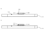
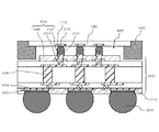
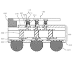
図1は、第1の実施形態に係る半導体装置の構成を示す断面図である。この半導体装置は、半導体チップ100、磁気シールド層400、及び配線基板200を備えている。半導体チップ100は磁気記憶素子10を有しており、かつ第1面に電極パッド110(本図で省略)を有している。磁気シールド層400は、少なくとも電極パッド110が露出した状態で半導体チップ100を被覆している。半導体チップ100は、バンプ310を介して配線基板200に実装されている。ここでの接続形態は、例えばフリップチップ接続である。半導体チップ100と配線基板200は、少なくとも一方が凸部を有しており、当該凸部上にバンプ310が設けられている。以下、詳細に説明する。
(First embodiment)
FIG. 1 is a cross-sectional view showing the configuration of the semiconductor device according to the first embodiment. The semiconductor device includes a
本実施形態において、凸部は配線基板200に設けられている。具体的には、配線基板200は、第1の配線基板210及び第2の配線基板220を有している。平面視において、第2の配線基板220は第1の配線基板210よりも小さい。第2の配線基板220は、バンプ230を介して第1の配線基板210の上に搭載されている。このような構成により、第2の配線基板220が凸部を構成している。そして第2の配線基板220のうち第1の配線基板210に対向していない面は、バンプ310を介して半導体チップ100に接続している。バンプ230,310は、例えば半田バンプである。また第1の配線基板210のうち半導体チップ100とは逆側の面には、外部接続端子としてハンダボール320が設けられている。
In the present embodiment, the convex portion is provided on the
磁気シールド層400は、少なくとも半導体チップ100の第1面(配線基板200に対向する面)の一部を覆っているが、平面視で第2の配線基板220とは重なっていない。具体的には、磁気シールド層400は、半導体チップ100のほぼ全面(側面を含む)を覆っているが、配線基板200に対向している領域に開口402を有している(後述する図25(a)に相当)。平面視において開口402は、第2の配線基板220よりも大きい。このため、磁気シールド層400は第2の配線基板220とは干渉せず、開口402の内側に第2の配線基板220が入り込む。磁気シールド層400は、軟磁性材料、例えば、鉄、パーマロイ、センダスト、珪素鋼、又はナノ結晶により形成されている。磁気シールド層400の厚さは、例えば0.05mm以上0.15mm以下である。
The
半導体チップ100と配線基板200の間の空間は、アンダーフィル樹脂510により封止されている。アンダーフィル樹脂510は、エポキシ系の樹脂であってもよいし、イミド系の樹脂であってもよい。本実施形態において、アンダーフィル樹脂510は、磁気シールド層400と第2の配線基板220の間にも形成されている。すなわち第2の配線基板220も、アンダーフィル樹脂510によって封止されている。
A space between the
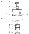
図2は、磁気記憶素子10の原理を説明するための図である。磁気記憶素子10は、磁気固定層12と磁気フリー層14とをトンネルバリア層16を介して対向させた構造を有している。図2(a)に示す磁気記憶素子10は、垂直スピンタイプの素子である。このタイプの磁気記憶素子10は、半導体チップ100に対して垂直方向の磁場によって書込及び消去が行われる。図2(b)に示す磁気記憶素子10は、水平スピンタイプの素子である。このタイプの磁気記憶素子10は、半導体チップ100に対して水平方向の磁場によって書込及び消去が行われる。いずれのタイプの磁気記憶素子10も、磁気固定層12と磁気フリー層14の磁化の向きが同一方向の場合は低抵抗となり、磁気固定層12と磁気フリー層14の磁化の向きが逆方向の場合は高抵抗となる、そして、トンネルバリア層16を通過するトンネル電流の大小を測定することにより、書き込みされている情報の読み出しが行われる。そして図1に示す磁気シールド層400は、図2(a)及び図2(b)のいずれのタイプの磁気記憶素子10に対しても磁気シールド効果を奏する。
FIG. 2 is a diagram for explaining the principle of the
図3は、磁気記憶素子10の構成を説明するための図である。図3(a)に示す磁気記憶素子10は、磁壁移動型の磁気記憶素子である。具体的には、磁気フリー層14が磁壁移動層になっており、2本のビット線13a,13bに接続している。そして磁気固定層12は読出線11に接続している。
FIG. 3 is a diagram for explaining the configuration of the
図3(b)に示す磁気記憶素子10はスピン注入型の磁気記憶素子である。具体的には、磁気フリー層14は一本のビット線13に接続しており、磁気固定層12は読出線11に接続している。
The
なお、図2及び図3を用いて磁気記憶素子10の原理及び構成を説明したが、本発明が適用できる磁気記憶素子10の構成はこれらに限定されず、例えば磁場移動型の磁気記憶素子であってもよい。
Although the principle and configuration of the
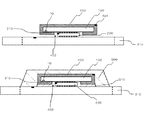
図4及び図5は、図1に示した半導体装置の製造方法を示す断面図である。まず図4(a)に示すように、個片化される前の第1の配線基板210に、バンプ230を用いて第2の配線基板220を搭載する。第1の配線基板210には位置合わせマーク212が設けられており、第1の配線基板210には位置合わせマーク222が設けられている。位置合わせマーク212,222は、例えば配線層の一部であり、保護層から露出している導体パターンである。このため、位置合わせマーク212と位置合わせマーク222の位置を検出することにより、第1の配線基板210上に第2の配線基板220を高い位置精度で搭載することができる。なお、第2の配線基板220は、第1の配線基板210のうち個片化される複数の領域それぞれに搭載される。
4 and 5 are cross-sectional views showing a method of manufacturing the semiconductor device shown in FIG. First, as shown in FIG. 4A, the
次いで図4(b)に示すように、第1の配線基板210上に搭載された各第2の配線基板220に、バンプ310を一括して形成する。
Next, as shown in FIG. 4B, bumps 310 are collectively formed on each
次いで図5(a)に示すように、磁気シールド層400で被覆された半導体チップ100を準備する。磁気シールド層400は、例えば複数の部品を半導体チップ100に取り付けることにより、形成することができる。
Next, as shown in FIG. 5A, the
次いで、バンプ310を用いて半導体チップ100を第2の配線基板220に搭載する。ここで、磁気シールド層400には位置合わせマーク404が設けられているため、半導体チップ100は高い位置精度で第2の配線基板220に搭載される。なお、位置合わせマーク404は、例えば磁気シールド層400に設けられた特定の形状(くぼみを含む)である。
Next, the
この状態において、磁気シールド層400と第1の配線基板210の間には、隙間が存在する。このようにすると、バンプ310が硬化する際に、半導体チップ100は自己整合的に第2の配線基板220に対して位置決めされる。
In this state, there is a gap between the
次いで図5(b)に示すように、毛細管現象を利用し、磁気シールド層400と第1の配線基板210の間の隙間を、アンダーフィル樹脂510で封止する。このとき、磁気シールド層400と第2の配線基板220の間の隙間にも、毛細管現象によりアンダーフィル樹脂510が浸透する。次いで、複数の半導体チップ100を封止樹脂500で個別に封止する。
Next, as shown in FIG. 5B, the gap between the
その後、ダイシングライン(点線で示す)に沿って第1の配線基板210を切断することにより、複数の半導体装置を個片化する。
Thereafter, the
次に、本実施形態の作用及び効果について説明する。本実施形態によれば、磁気シールド層400は、半導体チップ100の電極パッドを露出させるための開口402を有している。そして開口402は平面視で第2の配線基板220を内側に含んでいる。このため、半導体チップ100を配線基板200上に搭載したとき、第2の配線基板220の上面は磁気シールド層400の下面より半導体チップ100の近くに位置する。従って、バンプ310の高さを低くすることができる。そして、これに伴ってバンプ310の幅を小さくすることができる。これにより、バンプ310を狭いピッチで高密度に配置することができる。
Next, the operation and effect of this embodiment will be described. According to the present embodiment, the
(第2の実施形態)
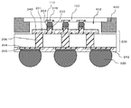
図6は、第2の実施形態に係る半導体装置の構成を示す断面図であり、第1の実施形態における図1に相当している。本実施形態に係る半導体装置は、封止樹脂500の形状を除いて、第1の実施形態に係る半導体装置と同様の構成である。具体的には、封止樹脂500の側面は、第1の配線基板210の側面と同一面を形成している。
(Second Embodiment)
FIG. 6 is a cross-sectional view showing the configuration of the semiconductor device according to the second embodiment, and corresponds to FIG. 1 in the first embodiment. The semiconductor device according to the present embodiment has the same configuration as that of the semiconductor device according to the first embodiment except for the shape of the sealing
図7は、図6に示した半導体装置の製造方法を示す断面図である。まず図7(a)に示すように、第1の配線基板210上に第2の配線基板220を搭載し、さらに第2の配線基板220上に、磁気シールド層400で被覆された半導体チップ100を搭載する。次いで、アンダーフィル樹脂510を形成する。ここまでの工程は、第1の実施形態と同様である。
FIG. 7 is a cross-sectional view showing a method for manufacturing the semiconductor device shown in FIG. First, as shown in FIG. 7A, the
次いで図7(b)に示すように、複数の半導体チップ100を封止樹脂500で一括封止する。その後、封止樹脂500及び第1の配線基板210をダイシングすることにより、複数の半導体装置を個片化する。
Next, as shown in FIG. 7B, the plurality of
本実施形態によっても、第1の実施形態と同様の効果を得ることができる。 Also according to this embodiment, the same effect as that of the first embodiment can be obtained.
(第3の実施形態)
図8は、第3の実施形態に係る半導体装置の製造方法を示す断面図である。本実施形態に係る半導体装置の製造方法は、アンダーフィル樹脂510の形成方法を除いて、第1又は第2の実施形態に係る半導体装置の製造方法と同様である。
(Third embodiment)
FIG. 8 is a cross-sectional view illustrating the method of manufacturing the semiconductor device according to the third embodiment. The manufacturing method of the semiconductor device according to this embodiment is the same as the manufacturing method of the semiconductor device according to the first or second embodiment, except for the formation method of the
まず図8(a)に示すように、第1の配線基板210上にバンプ230を形成する。次いで、第2の配線基板220の下面に絶縁性の樹脂フィルム(NCF:Non Conductive Film)512を、例えばラミネート法により設ける。次いで、第1の配線基板210上に第2の配線基板220を搭載する。これにより、第2の配線基板220と第1の配線基板210の間の空間は樹脂フィルム512により封止される。
First, as shown in FIG. 8A, bumps 230 are formed on the
次いで図8(b)に示すように、第2の配線基板220上にバンプ310を設ける。次いでバンプ310上及び第2の配線基板220上に、樹脂フィルム(NCF)514をラミネート法により設ける。これにより、アンダーフィル樹脂510が形成される(図8(c))。この段階において、アンダーフィル樹脂510は第2の配線基板220及びバンプ310を封止しているが、未だ硬化していない。
Next, as shown in FIG. 8B, bumps 310 are provided on the
次いで、第2の配線基板220上に、磁気シールド層400で被覆された半導体チップ100を搭載する。このとき、半導体チップ100はある程度の圧力で第2の配線基板220に押し付けられる。これにより、バンプ310は半導体チップ100に接触する。
Next, the
次いで、半導体チップ100、配線基板200、及びバンプ310を熱処理し、その後冷却する。詳細には、まず加熱により、アンダーフィル樹脂510を軟化させ、バンプ間を埋める。その後、徐々にアンダーフィル樹脂510は硬化し、これと並行して、バンプ310は溶融する。そして冷却によりバンプは凝固して、半導体チップ100に接合する。その後、封止樹脂500を設ける。
Next, the
本実施形態では、半導体チップ100が第2の配線基板220に接合される前に樹脂フィルム514が設けられているが、樹脂フィルム514は、第2の配線基板220の上面ではなく半導体チップ100の下面に設けられてもよい。
In the present embodiment, the
本実施形態によっても、第1の実施形態と同様の効果を得ることができる。また、第2の配線基板220に半導体チップ100を搭載する前に、アンダーフィル樹脂510を樹脂フィルム512,514で形成するため、バンプ230,310のピッチが小さくなっても、バンプ230,310をアンダーフィル樹脂510で十分封止することができる。
Also according to this embodiment, the same effect as that of the first embodiment can be obtained. Further, since the
(第4の実施形態)
図9は、第4の実施形態に係る半導体装置の構成を示す断面図である。本実施形態に係る半導体装置は、磁気シールド層400の形状を除いて、第1〜第3の実施形態のいずれかと同様である。
(Fourth embodiment)
FIG. 9 is a cross-sectional view showing the configuration of the semiconductor device according to the fourth embodiment. The semiconductor device according to this embodiment is the same as any one of the first to third embodiments except for the shape of the
本実施形態において、磁気シールド層400は、半導体チップ100の側面と対向している領域に湾曲部406を有している。すなわち半導体チップ100の側面と磁気シールド層400の間には、隙間が存在している。
In the present embodiment, the
本実施形態によっても、第1〜第3の実施形態と同様の効果を得ることができる。また磁気シールド層400が湾曲部406を有しているため、例えば薄い鋼板を折り曲げ加工することにより、磁気シールド層400の少なくとも一部を形成することができる。従って、磁気シールド層400の製造コストを低くすることができる。
Also according to the present embodiment, the same effects as those of the first to third embodiments can be obtained. Further, since the
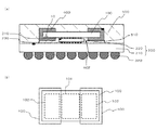
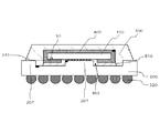
(第5の実施形態)
図10(a)は、第5の実施形態に係る半導体装置の構成を示す断面図であり、第1の実施形態における図1に相当している。図10(b)は、図10(a)に示した半導体装置の上面図である。本実施形態に係る半導体装置は、以下の点を除いて第1〜第3の実施形態のいずれかに係る半導体装置と同様の構成である。
(Fifth embodiment)
FIG. 10A is a cross-sectional view showing the configuration of the semiconductor device according to the fifth embodiment, and corresponds to FIG. 1 in the first embodiment. FIG. 10B is a top view of the semiconductor device shown in FIG. The semiconductor device according to the present embodiment has the same configuration as the semiconductor device according to any one of the first to third embodiments except for the following points.
まず、半導体チップ100は、メモリ領域102とメモリ無領域104を有している。メモリ領域102は、磁気記憶素子10が設けられている領域であり、メモリ無領域104は磁気記憶素子10が設けられていない領域である。メモリ無領域104には、例えばロジック回路が配置されている。そして磁気シールド層400は、平面視でメモリ領域102を覆っており、かつメモリ無領域104を覆っていない。
First, the
詳細には、本実施形態において磁気記憶素子10は、図2(a)に示した垂直スピンタイプの素子である。また半導体チップ100は矩形を有している。そしてメモリ領域102は、メモリ無領域104と比較して半導体チップ100の一辺に近い側に設けられている。そして磁気シールド層400は、半導体チップ100のうち配線基板200に対向している第1面から、側面を経由して、第1面とは逆側の面である第2面にかけて形成されている。
Specifically, in the present embodiment, the
具体的には、メモリ無領域104は半導体チップ100の中心側に設けられており、メモリ領域102は半導体チップ100の両脇に設けられている。そして半導体チップ100のメモリ領域102は、互いに異なる磁気シールド層400によってそれぞれ覆われている。各磁気シールド層400は、半導体チップ100の4つの側面のうち1つの側面を完全に覆っており、かつこの側面につながる2つの側面を覆っていない(後述する図24(a),(b)に相当)。なお、後述する図24(d)に示すように、磁気シールド層400は上記した2つの側面を部分的に覆っていてもよい。
Specifically, the
本実施形態によっても、第1〜第3の実施形態と同様の効果を得ることができる。また、半導体チップ100に対して垂直な方向の磁場に対しては、第1の実施形態に係る磁気シールド層400よりも、本実施形態に係る磁気シールド層400のほうがシールド効果が高い。従って、磁気記憶素子10に対して誤書込や誤消去が行われる可能性がさらに低くなる。
Also according to the present embodiment, the same effects as those of the first to third embodiments can be obtained. Further, the
(第6の実施形態)
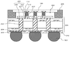
図11(a)は、第6の実施形態に係る半導体装置の構成を示す断面図であり、第1の実施形態における図1に相当している。図10(b)は、図10(a)に示した半導体装置の上面図である。本実施形態に係る半導体装置は、磁気シールド層400の形状を除いて第5の実施形態に係る半導体装置と同様の構成である。
(Sixth embodiment)
FIG. 11A is a cross-sectional view showing the configuration of the semiconductor device according to the sixth embodiment, and corresponds to FIG. 1 in the first embodiment. FIG. 10B is a top view of the semiconductor device shown in FIG. The semiconductor device according to this embodiment has the same configuration as that of the semiconductor device according to the fifth embodiment except for the shape of the
本実施形態において、磁気シールド層400は、湾曲部406を有している。湾曲部406の構成は、第4の実施形態と同様である。
In the present embodiment, the
本実施形態によっても、第5の実施形態と同様の効果を得ることができる。また第4の実施形態と同様に、磁気シールド層400の製造コストを低くすることができる。
Also in this embodiment, the same effect as that of the fifth embodiment can be obtained. Further, similarly to the fourth embodiment, the manufacturing cost of the
(第7の実施形態)
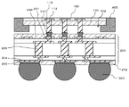
図12(a)は、第7の実施形態に係る半導体装置の構成を示す断面図である。本実施形態に係る半導体装置は、配線基板200の構成を除いて、第1〜第6の実施形態のいずれかと同様である。
(Seventh embodiment)
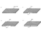
FIG. 12A is a cross-sectional view showing the configuration of the semiconductor device according to the seventh embodiment. The semiconductor device according to this embodiment is the same as that of any of the first to sixth embodiments except for the configuration of the
本実施形態において、配線基板200は、凸部250を有している。凸部250は、一枚の配線基板200の表面が部分的に凸になることにより、形成されている。凸部250は、磁気シールド層400の開口402内に入り込んでいる。そして凸部250の上面には、バンプ310が接続している。
In the present embodiment, the
図12(b)は、図12(a)の変形例を示す断面図である。本図に示す例において、凸部250は配線基板200のうち磁気シールド層400に対向しない部分の全域に形成されている。そして磁気シールド層400は、配線基板200のうち凸部250が形成されていない領域に当接していても良いし、この領域から離れていてもよい。
FIG.12 (b) is sectional drawing which shows the modification of Fig.12 (a). In the example shown in the drawing, the
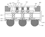
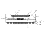
図13は、凸部250の構造の詳細を示す断面拡大図である。本図に示す例において、配線基板200は4層以上の多層配線基板である。凸部250は、保護層240、金属柱202、及び金属層203により構成されている。保護層240は、例えばソルダーレジストであり、配線基板200の上面を部分的に被覆している。ここでソルダーレジストは、例えば、エポキシ樹脂、アクリル樹脂、及びポリイミド樹脂の少なくとも一つを含んでいる。保護層240の厚さは、例えば20μm以上60μm以下である。金属柱202は、例えばCuにより形成されている。また配線基板200のうちハンダボール320が取り付けられる面には、保護層242が形成されている。
FIG. 13 is an enlarged cross-sectional view showing details of the structure of the
配線基板200のうち保護層240が形成されている領域には、電極201が形成されている。電極201は、平面視で磁気シールド層400の開口402の内側に位置している。そして電極201には、金属柱202が接続している。金属柱202は保護層240を貫通しており、上端が保護層240よりも上に位置している。金属柱202は例えばCuポストであり、例えば電解めっき法により形成されている。金属柱202の高さは、例えば60μm以上120μm以下である。
An
金属柱202の上端(上端面および側面の上端部を含む)には、金属層203が形成されている。金属層203は、例えばNi/Au、Ni/Pd/Au層であり、例えば無電解めっき法、又は電解めっき法により形成されている。金属層203は、バンプ310を金属柱202に接合させるために設けられている。
A
そして電極201は、コア層に設けられたビア206を介して電極204に接続している。電極204は配線基板200の裏面側に設けられており、金属層205を介してハンダボール320に接続している。
The
本実施形態によっても、第1〜第6の実施形態と同様の効果を得ることができる。 Also according to this embodiment, the same effects as those of the first to sixth embodiments can be obtained.
なお、図14に示すように、配線基板200はコア層の上面及び下面に配線を形成した2層基板であってもよい。この場合、コア層の上面に電極201が形成され、コア層の下面に電極204が形成される。
As shown in FIG. 14, the
(第8の実施形態)
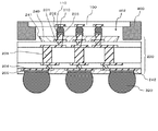
図15は、第8の実施形態に係る半導体装置の構成を示す断面図であり、第7の実施形態に係る図13に相当している。本実施形態に係る半導体装置は、以下を除いて第7の実施形態に係る半導体装置と同様の構成である。
(Eighth embodiment)
FIG. 15 is a cross-sectional view showing the configuration of the semiconductor device according to the eighth embodiment, and corresponds to FIG. 13 according to the seventh embodiment. The semiconductor device according to the present embodiment has the same configuration as the semiconductor device according to the seventh embodiment except for the following.
本実施形態において、配線基板200は最上層にビルドアップ領域207を有している。ビルドアップ領域207は、配線層を部分的にビルドアップすることにより形成されている。そして保護層240は、ビルドアップ領域207上のみに形成されている。ビルドアップ領域207は、平面視で磁気シールド層400の開口402と重なる部分に形成されている。そしてビルドアップ領域207及び保護層240により、凸部が形成されている。この凸部は、開口402内に入り込んでいる。
In the present embodiment, the
また、電極201上には金属柱202が形成されておらず、バンプ310は、電極201に直接接続している。ただし電極201は、上面に、バンプ310との接合を確保するために、Ni/Au、Ni/Pd/Auなどの金属層を有している。
Further, the
また、ビルドアップ領域207の一つ下の配線層に位置する配線層では、配線はビルドアップ領域207で覆われている部分のみに形成されている。
Further, in the wiring layer located in the wiring layer immediately below the build-up
本実施形態によっても、第7の実施形態と同様の効果を得ることができる。 Also in this embodiment, the same effect as that of the seventh embodiment can be obtained.
なお、本実施形態において、保護層240は、配線基板200のうち半導体チップ100に対向する面の全面に形成されても良い。この場合、ビルドアップ領域207の一つ下の配線層に位置する配線層のうちビルドアップ領域207で覆われていない部分にも、配線を形成することができる。
In the present embodiment, the
また図16に示すように、ビルドアップ領域207は、平面視で磁気シールド層400と重ならない領域である限りにおいて、開口402と重ならない場所(例えば平面視で磁気シールド層400の外側に位置する部分)にも形成されて良い。
As shown in FIG. 16, the build-up
また図17に示すように、配線基板200内における電極201と電極204は、一つのビア206によって直接接続されてもよい。
As shown in FIG. 17, the
(第9の実施形態)
図18は、第9の実施形態に係る半導体装置の構成を示す断面図である。本実施形態に係る半導体装置は、以下の点を除いて、第7の実施形態に係る半導体装置と同様の構成である。
(Ninth embodiment)
FIG. 18 is a cross-sectional view showing the configuration of the semiconductor device according to the ninth embodiment. The semiconductor device according to this embodiment has the same configuration as that of the semiconductor device according to the seventh embodiment except for the following points.
まず、磁気シールド層400が半導体チップ100の側面の一部には形成されていない。そして保護層240は、平面視で、半導体チップ100の側面のうち磁気シールド層400が形成されていない部分から半導体チップ100の内側から外側にかけて連続的に形成されている。
First, the
本実施形態によっても、第7の実施形態と同様の効果を得ることができる。 Also in this embodiment, the same effect as that of the seventh embodiment can be obtained.
(第10の実施形態)
図19は、第10の実施形態に係る半導体装置の構成を示す断面図である。本実施形態に係る半導体装置は、以下の点を除いて、第8の実施形態に係る半導体装置と同様の構成である。
(Tenth embodiment)
FIG. 19 is a cross-sectional view showing the configuration of the semiconductor device according to the tenth embodiment. The semiconductor device according to the present embodiment has the same configuration as that of the semiconductor device according to the eighth embodiment except for the following points.
まず、半導体チップ100は、金属柱112を有している。金属柱112は電極パッド110上に形成されている。電極パッド110を含む多層配線層上には、保護層120が形成されている。保護層120は、電極パッド110上に位置する開口が設けられているが、この開口内に金属柱112が形成されている。金属柱112は、例えばCuから構成されている。金属柱112は、保護層120よりも高く、上端が保護層120より凸になっている。金属柱112の高さは、例えば60μm以上120μm以下である。
First, the
そして、金属柱112の端面にバンプ310が形成されている。配線基板200には金属柱202が設けられていないため、バンプ310は保護層240に設けられた開口内に入り込む。この開口は、電極201上に位置している。そしてバンプ310は、アンダーバンプメタル(図示せず)を介して電極201に接続している。
A
図20は、図19の第1の変形例を示す断面図である。この変形例は、以下の点を除いて図19と同様の構成である。まず、保護層240は配線基板200のうち半導体チップ100に対向している面の全面に形成されている。そして保護層240により被覆されている配線層は、平面視で磁気シールド層400と重なる領域にも配線を有している。
FIG. 20 is a cross-sectional view showing a first modification of FIG. This modification has the same configuration as that of FIG. 19 except for the following points. First, the
すなわち本実施形態では、半導体チップ100が凸部として金属柱112を有していることになる。金属柱112は保護層120よりも高いため、金属柱112を設けることにより、第7の実施形態において配線基板200に凸部を設けたときと同様の効果を得ることができる。
That is, in this embodiment, the
図21は、図19の第2の変形例を示す断面図である。この変形例は、以下の点を除いて図19と同様の構成である。まず、磁気シールド層400が半導体チップ100の側面の一部には形成されていない。そして保護層240は、平面視で、半導体チップ100の側面のうち磁気シールド層400が形成されていない部分から半導体チップ100の内側から外側にかけて連続的に形成されている。
FIG. 21 is a cross-sectional view showing a second modification of FIG. This modification has the same configuration as that of FIG. 19 except for the following points. First, the
本実施形態によっても、第8の実施形態と同様の効果を得ることができる。 Also in this embodiment, the same effect as that in the eighth embodiment can be obtained.
(第11の実施形態)
図22は、第11の実施形態に係る半導体装置の構成を示す断面図である。本実施形態に係る半導体装置は、保護層240の端面241が上を向く方向に傾斜している点を除いて、第7〜第10の実施形態のいずれかに係る半導体装置と同様の構成である。
(Eleventh embodiment)
FIG. 22 is a cross-sectional view showing the configuration of the semiconductor device according to the eleventh embodiment. The semiconductor device according to this embodiment has the same configuration as that of the semiconductor device according to any of the seventh to tenth embodiments, except that the end surface 241 of the
本実施形態によっても、第7の実施形態と同様の効果を得ることができる。また配線基板200上に半導体チップ100を搭載するときに、端面241に磁気シールド層400の下端が当接した場合でも、端面241に沿って磁気シールド層400の下端がスライドすることにより、半導体チップ100は、自己整合的に正しい位置に移動する。従って、さらに確実に半導体チップ100を配線基板200に実装することができる。
Also in this embodiment, the same effect as that of the seventh embodiment can be obtained. Further, when the
なお、図23に示すように、保護層240の端面241は、下を向く方向に傾斜していてもよい。
As shown in FIG. 23, the end surface 241 of the
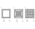
図24の各図、及び図25の各図は、第1〜第11の実施形態における磁気シールド層400の変形例を示す斜視図である。上記した各実施形態では、磁気シールド層400は、図24(a)、図24(b)、及び図25(a)のいずれかに示す形状を有していた。しかし磁気シールド層400の形状はこれらに限定されず、例えば図24、図25の各図に示す形状としてもよい。
Each drawing in FIG. 24 and each drawing in FIG. 25 are perspective views showing modifications of the
図24(b)に示す例は、図24(a)に示す例に対し、磁気シールド層400の幅が半導体チップ100の幅よりも狭い点が異なる。そして半導体チップ100の縁は磁気シールド層400に被覆されていない。
The example shown in FIG. 24B is different from the example shown in FIG. 24A in that the width of the
図24(c)に示す例は、図24(a)に示す例に対し、磁気シールド層400が半導体チップ100の一辺の近傍にのみ設けられている点が異なる。
The example shown in FIG. 24C is different from the example shown in FIG. 24A in that the
図24(d)に示す例では、磁気シールド層400は、直方体のうち半導体チップ100が差し込まれる側面のみが開口している形状を有している。そして2つの磁気シールド層400が、半導体チップ100のうち互いに対向している2つの側面側から、それぞれ差し込まれている。
In the example shown in FIG. 24D, the
図24(e)に示す例は、図24(c)に示す例に対し、磁気シールド層400の幅が半導体チップ100の幅よりも狭く、かつ長手方向に長い点が異なる。磁気シールド層400の端部は、半導体チップ100の能動面(電極パッドが形成されている面)のうち半導体チップ100の一側面の近くから、この一側面の反対側の側面を経由し、さらに半導体チップ100の裏面のうち上記した一側面の近くまで延伸している。
The example shown in FIG. 24E is different from the example shown in FIG. 24C in that the
図25(b)に示す例では、磁気シールド層400は、図25(a)に示す例に対し、開口402が半導体チップ100のうち互いに対向している2つの側面につながっている点が異なる。そして磁気シールド層400は、これら2つの側面は覆っておらず、残りの2つの側面を覆っている。
In the example shown in FIG. 25B, the
図25(c)に示す例では、磁気シールド層400は、図25(b)に示す例に対し、開口402が、半導体チップ100のうち互いに対向している2つの側面にまで連続して形成されているが、これら2つの側面の他の部分は磁気シールド層400によって被覆されている点が異なる。
In the example shown in FIG. 25C, the
図25(d)に示す例では、磁気シールド層400は、図25(a)に示す例に対し、互いに対向している2側面を覆っていない点が異なる。
The example shown in FIG. 25D is different from the example shown in FIG. 25A in that the
図26は、図24の各図に示した例における開口402の形状の一例を示す図である。図27は、図25の各図に示した例における開口402の形状の一例を示す図である。いずれの例においても、開口402は、半導体チップ100のうち電極パッドが設けられた領域に形成されている。
FIG. 26 is a diagram showing an example of the shape of the
図26(a)及び(b)に示す例では、半導体チップ100の電極パッドは、半導体チップ100のうち互いに対向する2側面に沿って形成されている。そして開口402も、半導体チップ100のうち互いに対向する2側面に沿って延伸している。そして、図26(a)に示すように、開口402が磁気シールド層400の中で閉じている形状となる場合もあれば、図26(b)に示すように、開口402が磁気シールド層400の縁につながって開放されている形状となる場合もある。
In the example shown in FIGS. 26A and 26B, the electrode pads of the
図26(c)及び図27(a)に示す例では、半導体チップ100の電極パッドは、半導体チップ100の縁を除いた全面に形成されている。この場合、開口402は、半導体チップ100の能動面に対向する部分のうち、縁を除いた領域に形成される。
In the example shown in FIG. 26C and FIG. 27A, the electrode pads of the
図27(b)に示す例では、半導体チップ100の電極パッドは、半導体チップ100の4つの側面それぞれに沿って形成されている。そして開口402も、半導体チップ100の4つの側面それぞれに沿って延伸している。
In the example shown in FIG. 27B, the electrode pads of the
図27(c)に示す例では、開口402は、電極パッドそれぞれ別に設けられている。
In the example shown in FIG. 27C, the
なお、図24及び図25に示した各例において、図28に示すように、磁気シールド層400は、半導体チップ100の側面に沿って形成されている部分が、半導体チップ100の能動面及びその反対面に対向している部分よりも厚くなっていてもよい。
In each example shown in FIG. 24 and FIG. 25, as shown in FIG. 28, the
磁気シールド層400は、磁束を磁気シールド層400の内部を通過させることにより、半導体チップ100に磁場が加わらないようにするものである。そして、磁気シールド層400のうち最も磁束密度が高くなるのは、磁気シールド層400のうち半導体チップ100の側面に沿っている部分である。図28に示す例では、磁気シールド層400のうち半導体チップ100の側面に沿っている部分が、他の部分よりも厚くなっている。このため、この部分における磁束の通過容量が増大する。このため、磁気シールド層400の磁気シールド能力が向上する。
The
また磁気シールド層400が、半導体チップ100の側面を経由して半導体チップ100の一面(能動面)側から他面(裏面)側に回り込んでいる場合、磁気シールド層400には、図26の各図に示したように、この側面に沿った長尺形状の開口402を形成しないのが好ましい。
In addition, when the
上記したように、磁気シールド層400は、磁束を磁気シールド層400の内部を通過させることにより、半導体チップ100に磁界が加わらないようにするものである。半導体チップ100の側面を経由して半導体チップ100の一面(能動面)側から他面(裏面)側に回り込んでいる場合、磁束は、磁気シールド層400のうち半導体チップ100の一面(能動面)側に位置する部分から、半導体チップ100の側面に対向している部分を経由して、半導体チップ100の他面(裏面)側に位置する部分に流れる。ここで磁気シールド層400に、上記した側面に沿った長尺形状の開口402を形成してしまうと、この側面近傍において、磁束が流れる部分が減少してしまい、この部分における磁束の通過容量が減少してしまう。この場合、磁気シールド層400の磁気シールド能力が低下してしまう。
As described above, the
(第12の実施形態)
図29は、第12の実施形態に係る半導体装置の構成を示す断面図である。本実施形態に係る半導体装置は、以下の点を除いて第1〜第11の実施形態に係る半導体装置のいずれかと同様の構成である。なお図29は、第2の実施形態と同様の場合を図示している。
(Twelfth embodiment)
FIG. 29 is a cross-sectional view showing the configuration of the semiconductor device according to the twelfth embodiment. The semiconductor device according to this embodiment has the same configuration as that of any of the semiconductor devices according to the first to eleventh embodiments except for the following points. FIG. 29 shows a case similar to that of the second embodiment.
まず、磁気記憶素子10は水平スピンタイプの素子である。そして、磁気シールド層400は、半導体チップ100の裏面側(図中上側の面)にのみ設けられている。また、配線基板200の凸部(本図に示す例では第2の配線基板220)以外の領域のうち半導体チップ100と対向している部分には、素子20が搭載されている。素子20は、半導体チップであってもよいし、他のディスクリート部品であってもよい。
First, the
本実施形態によれば、配線基板200のうち平面視で半導体チップ100と重なる領域に、半導体チップ100以外の電子部品を搭載することができる。
According to the present embodiment, an electronic component other than the
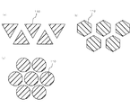
なお、上記した各実施形態において、電極パッド110の平面形状は矩形である必要はない。例えば図30に示すように、電極パッド110は正三角形(図30(a))、正六角形(図30(b))又は円形(図30(c))であってもよい。この場合、電極パッド110を千鳥配置することにより、電極パッド110の配置密度を高めることができる。
In each of the embodiments described above, the planar shape of the
以上、図面を参照して本発明の実施形態について述べたが、これらは本発明の例示であり、上記以外の様々な構成を採用することもできる。 As mentioned above, although embodiment of this invention was described with reference to drawings, these are the illustrations of this invention, Various structures other than the above are also employable.
10 磁気記憶素子
11 読出線
12 磁気固定層
13 ビット線
13a ビット線
13b ビット線
14 磁気フリー層
16 トンネルバリア層
20 素子
100 半導体チップ
102 メモリ領域
104 メモリ無領域
110 電極パッド
112 金属柱
120 保護層
200 配線基板
201 電極
202 金属柱
203 金属層
204 電極
205 金属層
206 ビア
207 ビルドアップ領域
210 配線基板
212 位置合わせマーク
220 配線基板
222 位置合わせマーク
230 バンプ
240 保護層
241 端面
242 保護層
250 凸部
310 バンプ
320 ハンダボール
400 磁気シールド層
402 開口
404 位置合わせマーク
406 湾曲部
500 封止樹脂
510 アンダーフィル樹脂
512 樹脂フィルム
514 樹脂フィルム
DESCRIPTION OF
Claims (17)
少なくとも前記電極パッドが露出した状態で前記半導体チップを被覆する磁気シールド層と、
前記半導体チップがバンプを介して接続された配線基板と、
を備え、
前記半導体チップと前記配線基板は、少なくとも一方が凸部を有しており、当該凸部上に前記バンプが設けられている半導体装置。 A semiconductor chip having a magnetic memory element and having an electrode pad on the first surface;
A magnetic shield layer covering the semiconductor chip with at least the electrode pad exposed;
A wiring board to which the semiconductor chip is connected via bumps;
With
At least one of the semiconductor chip and the wiring board has a convex portion, and the bump is provided on the convex portion.
前記磁気シールド層は、少なくとも前記半導体チップの前記第1面の一部を覆っており、
前記凸部は、前記磁気シールド層のうち前記第1面を覆っている部分とは重なっていない半導体装置。 The semiconductor device according to claim 1,
The magnetic shield layer covers at least a part of the first surface of the semiconductor chip;
The convex portion is a semiconductor device that does not overlap a portion of the magnetic shield layer that covers the first surface.
前記半導体チップと前記配線基板の間の空間を封止する樹脂層を備え、
前記樹脂層は、前記磁気シールド層と前記凸部の間にも形成されている半導体装置。 The semiconductor device according to claim 2,
A resin layer that seals a space between the semiconductor chip and the wiring board;
The resin layer is a semiconductor device formed also between the magnetic shield layer and the convex portion.
前記凸部は前記配線基板に設けられている半導体装置。 The semiconductor device according to claim 1,
The convex portion is a semiconductor device provided on the wiring board.
前記配線基板は、第1の配線基板と、前記第1の配線基板上に設けられた第2の配線基板を有しており、
前記凸部は前記第2の配線基板である半導体装置。 The semiconductor device according to claim 4,
The wiring board has a first wiring board and a second wiring board provided on the first wiring board;
The convex portion is a semiconductor device which is the second wiring board.
前記配線基板は、
部分的に形成された保護膜と、
前記保護膜を貫通している金属柱と、
を有しており、
前記凸部は、前記保護膜及び前記金属柱である半導体装置。 The semiconductor device according to claim 4,
The wiring board is
A partially formed protective film;
A metal pillar penetrating the protective film;
Have
The convex part is the semiconductor device which is the protective film and the metal pillar.
前記配線基板は、部分的にビルドアップ領域を有しており、
前記凸部は前記ビルドアップ領域である半導体装置。 The semiconductor device according to claim 4,
The wiring board partially has a build-up region,
The semiconductor device in which the convex portion is the build-up region.
前記凸部は前記半導体チップに設けられている半導体装置。 The semiconductor device according to claim 1,
The convex portion is a semiconductor device provided on the semiconductor chip.
前記半導体チップは、前記凸部が設けられている面に保護膜を有しており、
前記凸部は、前記保護膜よりも高い半導体装置。 The semiconductor device according to claim 8,
The semiconductor chip has a protective film on the surface provided with the convex portion,
The convex portion is a semiconductor device higher than the protective film.
前記凸部は前記電極パッド上に形成された金属柱である半導体装置。 The semiconductor device according to claim 8 or 9,
The protrusion is a semiconductor device which is a metal pillar formed on the electrode pad.
前記半導体チップは、前記磁気記憶素子が形成されているメモリ有領域と、前記磁気記憶素子が形成されていないメモリ無領域とを有しており、
前記磁気シールド層は、少なくとも平面視で前記メモリ有領域と重なる領域に形成されている半導体装置。 In the semiconductor device according to any one of claims 1 to 10,
The semiconductor chip has a memory area in which the magnetic memory element is formed and a memory non-area in which the magnetic memory element is not formed,
The semiconductor device, wherein the magnetic shield layer is formed in a region overlapping at least the memory presence region in plan view.
前記磁気記憶素子は、前記半導体チップに対して垂直な方向の磁場によって書き込みが行われ、
前記磁気シールド層は、前記半導体チップの前記第1面から側面を経由して、前記第1面とは反対側の面である第2面にかけて形成されている半導体装置。 The semiconductor device according to any one of claims 1 to 11,
The magnetic memory element is written by a magnetic field in a direction perpendicular to the semiconductor chip,
The magnetic shield layer is a semiconductor device formed from the first surface of the semiconductor chip to a second surface that is a surface opposite to the first surface via a side surface.
前記半導体チップは矩形であり、
前記磁気シールド層は、
前記一面に対向する領域に前記電極パッドを露出させるための開口を有しており、
前記半導体チップの一辺に位置する前記側面を経由するように形成されており、かつ前記一辺の近くには、前記一辺に沿った長尺形状を有する前記開口が形成されていない半導体装置。 The semiconductor device according to claim 12,
The semiconductor chip is rectangular,
The magnetic shield layer is
Having an opening for exposing the electrode pad in a region facing the one surface;
A semiconductor device which is formed so as to pass through the side face located on one side of the semiconductor chip and in which the opening having a long shape along the one side is not formed near the one side.
前記磁気シールド層は、前記側面に対向する領域が、前記第1面に対向する領域及び前記第2面に対向する領域よりも厚い半導体装置。 The semiconductor device according to claim 12 or 13,
The magnetic shield layer is a semiconductor device in which a region facing the side surface is thicker than a region facing the first surface and a region facing the second surface.
前記半導体チップに垂直な断面で見た場合、前記磁気シールド層は、前記側面に対向する領域が湾曲している半導体装置。 The semiconductor device according to claim 12,
When viewed in a cross section perpendicular to the semiconductor chip, the magnetic shield layer is a semiconductor device in which a region facing the side surface is curved.
前記磁気記憶素子は、前記半導体チップに対して水平な方向の磁場によって書き込みが行われ、
前記磁気シールド層は、前記半導体チップのうち前記電極パッドが形成されていない面のみに形成されている半導体装置。 The semiconductor device according to any one of claims 1 to 11,
The magnetic memory element is written by a magnetic field in a direction horizontal to the semiconductor chip,
The magnetic shield layer is a semiconductor device formed only on a surface of the semiconductor chip where the electrode pad is not formed.
前記半導体チップを配線基板にバンプを介して接続する工程と、
を備え、
前記半導体チップと前記配線基板は、少なくとも一方が凸部を有しており、当該凸部上に前記バンプが設けられている半導体装置の製造方法。
Covering a semiconductor chip having a magnetic memory element and having an electrode pad on the first surface with a magnetic shield layer so that at least the electrode pad is exposed;
Connecting the semiconductor chip to a wiring board via bumps;
With
A method of manufacturing a semiconductor device, wherein at least one of the semiconductor chip and the wiring board has a convex portion, and the bump is provided on the convex portion.
Priority Applications (8)
| Application Number | Priority Date | Filing Date | Title |
|---|---|---|---|
| JP2010255088A JP2012109307A (en) | 2010-11-15 | 2010-11-15 | Semiconductor device, and method of manufacturing semiconductor device |
| US13/200,944 US8749033B2 (en) | 2010-11-15 | 2011-10-05 | Semiconductor device and method of manufacturing semiconductor device |
| TW100136272A TWI529899B (en) | 2010-11-15 | 2011-10-06 | Semiconductor device and method of manufacturing semiconductor device |
| TW105104845A TWI585935B (en) | 2010-11-15 | 2011-10-06 | Semiconductor device and method of manufacturing semiconductor device |
| CN201110360175.XA CN102468275B (en) | 2010-11-15 | 2011-11-14 | Semiconductor device and method of manufacturing semiconductor device |
| CN201410783835.9A CN104716256B (en) | 2010-11-15 | 2011-11-14 | Semiconductor devices |
| US14/273,177 US9324663B2 (en) | 2010-11-15 | 2014-05-08 | Semiconductor device including a plurality of magnetic shields |
| HK15110131.2A HK1209524A1 (en) | 2010-11-15 | 2015-10-15 | Semiconductor device |
Applications Claiming Priority (1)
| Application Number | Priority Date | Filing Date | Title |
|---|---|---|---|
| JP2010255088A JP2012109307A (en) | 2010-11-15 | 2010-11-15 | Semiconductor device, and method of manufacturing semiconductor device |
Related Child Applications (1)
| Application Number | Title | Priority Date | Filing Date |
|---|---|---|---|
| JP2015043217A Division JP6058051B2 (en) | 2015-03-05 | 2015-03-05 | Semiconductor device |
Publications (1)
| Publication Number | Publication Date |
|---|---|
| JP2012109307A true JP2012109307A (en) | 2012-06-07 |
Family
ID=46047038
Family Applications (1)
| Application Number | Title | Priority Date | Filing Date |
|---|---|---|---|
| JP2010255088A Pending JP2012109307A (en) | 2010-11-15 | 2010-11-15 | Semiconductor device, and method of manufacturing semiconductor device |
Country Status (5)
| Country | Link |
|---|---|
| US (2) | US8749033B2 (en) |
| JP (1) | JP2012109307A (en) |
| CN (2) | CN104716256B (en) |
| HK (1) | HK1209524A1 (en) |
| TW (2) | TWI529899B (en) |
Cited By (9)
| Publication number | Priority date | Publication date | Assignee | Title |
|---|---|---|---|---|
| JP2013145844A (en) * | 2012-01-16 | 2013-07-25 | Dainippon Printing Co Ltd | Semiconductor device |
| JP2015053450A (en) * | 2013-09-09 | 2015-03-19 | 株式会社東芝 | Semiconductor device and manufacturing method of the same |
| JP2015065223A (en) * | 2013-09-24 | 2015-04-09 | 株式会社東芝 | Semiconductor device and method of manufacturing the same |
| JP2015111735A (en) * | 2015-03-05 | 2015-06-18 | ルネサスエレクトロニクス株式会社 | Semiconductor device |
| JP2016511939A (en) * | 2013-02-08 | 2016-04-21 | クアルコム,インコーポレイテッド | Small form factor magnetic shield for magnetoresistive random access memory (MRAM) |
| US9324663B2 (en) | 2010-11-15 | 2016-04-26 | Renesas Electronics Corporation | Semiconductor device including a plurality of magnetic shields |
| JP2016072493A (en) * | 2014-09-30 | 2016-05-09 | 新光電気工業株式会社 | Semiconductor device and manufacturing method of the same |
| KR20160128796A (en) * | 2015-04-29 | 2016-11-08 | 삼성전자주식회사 | Magneto-resistive chip package including a shielding structure |
| WO2020116088A1 (en) * | 2018-12-03 | 2020-06-11 | ソニーセミコンダクタソリューションズ株式会社 | Semiconductor device and imaging device |
Families Citing this family (16)
| Publication number | Priority date | Publication date | Assignee | Title |
|---|---|---|---|---|
| US9583444B2 (en) * | 2013-08-20 | 2017-02-28 | Infineon Technologies Ag | Method for applying magnetic shielding layer, method for manufacturing a die, die and system |
| WO2015047324A1 (en) * | 2013-09-27 | 2015-04-02 | Intel Corporation | Magnetic field shielding for packaging build-up architectures |
| CN104598858B (en) * | 2013-11-01 | 2018-09-28 | 北京嘉岳同乐极电子有限公司 | Ultra-thin magnetic head and card reader |
| KR102187809B1 (en) | 2014-02-21 | 2020-12-07 | 삼성전자주식회사 | The method of fabricating a semiconductor package including a magnetic shield |
| US9954163B2 (en) * | 2014-05-15 | 2018-04-24 | Everspin Technologies, Inc. | Structures and methods for shielding magnetically sensitive components |
| JP6280014B2 (en) * | 2014-09-30 | 2018-02-14 | 新光電気工業株式会社 | Semiconductor device and manufacturing method thereof |
| KR102437673B1 (en) | 2015-09-09 | 2022-08-26 | 삼성전자주식회사 | Semiconductor device |
| CN107978531A (en) * | 2016-10-25 | 2018-05-01 | 上海磁宇信息科技有限公司 | The method for shielding of magnetic memory chip encapsulation |
| US10103125B2 (en) | 2016-11-28 | 2018-10-16 | Taiwan Semiconductor Manufacturing Co., Ltd. | Chip package structure and method for forming the same |
| JP6680705B2 (en) * | 2017-02-10 | 2020-04-15 | キオクシア株式会社 | Semiconductor device and manufacturing method thereof |
| CN108962836A (en) * | 2017-05-17 | 2018-12-07 | 上海磁宇信息科技有限公司 | Using the magnetic screen packaging part and magnetic screen packaging part method of magnetic plastic packaging material |
| CN108962837B (en) * | 2017-05-17 | 2020-02-18 | 上海磁宇信息科技有限公司 | SoC chip local magnetic shielding packaging method and SoC chip local magnetic shielding packaging piece |
| WO2020071493A1 (en) * | 2018-10-05 | 2020-04-09 | 株式会社村田製作所 | Module |
| US10998489B2 (en) * | 2019-01-14 | 2021-05-04 | Nxp B.V. | Magnetic shielding structure for MRAM array |
| CN112103269B (en) * | 2020-08-07 | 2022-09-20 | 珠海越亚半导体股份有限公司 | Embedded packaging structure with shielding cavity and manufacturing method thereof |
| US11610848B2 (en) * | 2021-06-07 | 2023-03-21 | Taiwan Semiconductor Manufacturing Company, Ltd. | Semiconductor package, semiconductor device and shielding housing of semiconductor package |
Citations (6)
| Publication number | Priority date | Publication date | Assignee | Title |
|---|---|---|---|---|
| JP2002203925A (en) * | 2000-12-28 | 2002-07-19 | Fujitsu Ltd | External connection terminal and semiconductor device |
| JP2003100942A (en) * | 2001-09-20 | 2003-04-04 | Hitachi Ltd | Semiconductor device |
| JP2003115578A (en) * | 2001-10-05 | 2003-04-18 | Canon Inc | Nonvolatile solid magnetic memory, its manufacturing method and multichip package |
| JP2003247441A (en) * | 2002-02-21 | 2003-09-05 | Nissan Motor Co Ltd | Control device for hybrid type vehicle |
| JP2006511936A (en) * | 2002-12-18 | 2006-04-06 | コーニンクレッカ フィリップス エレクトロニクス エヌ ヴィ | Torrent resistant packaging and approach |
| JP2010141018A (en) * | 2008-12-10 | 2010-06-24 | Shinko Electric Ind Co Ltd | Wiring board and method of manufacturing the same |
Family Cites Families (24)
| Publication number | Priority date | Publication date | Assignee | Title |
|---|---|---|---|---|
| JPH1022341A (en) * | 1996-07-05 | 1998-01-23 | Oki Electric Ind Co Ltd | Mounting method for bga package and mounted structure |
| US5902690A (en) * | 1997-02-25 | 1999-05-11 | Motorola, Inc. | Stray magnetic shielding for a non-volatile MRAM |
| US6625040B1 (en) * | 2000-08-31 | 2003-09-23 | Micron Technology, Inc. | Shielded PC board for magnetically sensitive integrated circuits |
| US6906396B2 (en) * | 2002-01-15 | 2005-06-14 | Micron Technology, Inc. | Magnetic shield for integrated circuit packaging |
| JP3879576B2 (en) | 2002-04-16 | 2007-02-14 | ソニー株式会社 | Magnetic non-volatile memory element magnetic shield package |
| JP3923368B2 (en) | 2002-05-22 | 2007-05-30 | シャープ株式会社 | Manufacturing method of semiconductor device |
| JP2010093277A (en) | 2002-06-25 | 2010-04-22 | Renesas Technology Corp | Semiconductor integrated circuit device |
| JP2004047656A (en) * | 2002-07-11 | 2004-02-12 | Sony Corp | Magnetic non-volatile memory device and its manufacturing method |
| US20040032010A1 (en) * | 2002-08-14 | 2004-02-19 | Kools Jacques Constant Stefan | Amorphous soft magnetic shielding and keeper for MRAM devices |
| JP2004172251A (en) | 2002-11-19 | 2004-06-17 | Renesas Technology Corp | Method and apparatus for packaging semiconductor device |
| JP4013140B2 (en) * | 2003-01-15 | 2007-11-28 | ソニー株式会社 | Magnetic memory device |
| US6940153B2 (en) * | 2003-02-05 | 2005-09-06 | Hewlett-Packard Development Company, L.P. | Magnetic shielding for magnetic random access memory card |
| US20060289970A1 (en) * | 2005-06-28 | 2006-12-28 | Dietmar Gogl | Magnetic shielding of MRAM chips |
| KR100691632B1 (en) * | 2006-05-16 | 2007-03-12 | 삼성전기주식회사 | Semiconductor chip, method of manufacturing the semiconductor chip and semiconductor chip package |
| US7795708B2 (en) * | 2006-06-02 | 2010-09-14 | Honeywell International Inc. | Multilayer structures for magnetic shielding |
| US8269319B2 (en) * | 2006-10-13 | 2012-09-18 | Tessera, Inc. | Collective and synergistic MRAM shields |
| US7598596B2 (en) * | 2006-11-21 | 2009-10-06 | Freescale Semiconductor, Inc. | Methods and apparatus for a dual-metal magnetic shield structure |
| JP4332567B2 (en) * | 2007-03-27 | 2009-09-16 | Okiセミコンダクタ株式会社 | Manufacturing method and mounting method of semiconductor device |
| TWI339432B (en) * | 2007-08-13 | 2011-03-21 | Ind Tech Res Inst | Magnetic shielding package structure of a magnetic memory device |
| JP5423944B2 (en) | 2008-06-26 | 2014-02-19 | 日本電気株式会社 | Magnetic random access memory |
| US7799602B2 (en) * | 2008-12-10 | 2010-09-21 | Stats Chippac, Ltd. | Semiconductor device and method of forming a shielding layer over a semiconductor die after forming a build-up interconnect structure |
| JP5470602B2 (en) | 2009-04-01 | 2014-04-16 | ルネサスエレクトロニクス株式会社 | Magnetic storage |
| JP2012109307A (en) | 2010-11-15 | 2012-06-07 | Renesas Electronics Corp | Semiconductor device, and method of manufacturing semiconductor device |
| US8791015B2 (en) * | 2011-04-30 | 2014-07-29 | Stats Chippac, Ltd. | Semiconductor device and method of forming shielding layer over active surface of semiconductor die |
-
2010
- 2010-11-15 JP JP2010255088A patent/JP2012109307A/en active Pending
-
2011
- 2011-10-05 US US13/200,944 patent/US8749033B2/en active Active
- 2011-10-06 TW TW100136272A patent/TWI529899B/en active
- 2011-10-06 TW TW105104845A patent/TWI585935B/en active
- 2011-11-14 CN CN201410783835.9A patent/CN104716256B/en not_active Expired - Fee Related
- 2011-11-14 CN CN201110360175.XA patent/CN102468275B/en not_active Expired - Fee Related
-
2014
- 2014-05-08 US US14/273,177 patent/US9324663B2/en active Active
-
2015
- 2015-10-15 HK HK15110131.2A patent/HK1209524A1/en not_active IP Right Cessation
Patent Citations (6)
| Publication number | Priority date | Publication date | Assignee | Title |
|---|---|---|---|---|
| JP2002203925A (en) * | 2000-12-28 | 2002-07-19 | Fujitsu Ltd | External connection terminal and semiconductor device |
| JP2003100942A (en) * | 2001-09-20 | 2003-04-04 | Hitachi Ltd | Semiconductor device |
| JP2003115578A (en) * | 2001-10-05 | 2003-04-18 | Canon Inc | Nonvolatile solid magnetic memory, its manufacturing method and multichip package |
| JP2003247441A (en) * | 2002-02-21 | 2003-09-05 | Nissan Motor Co Ltd | Control device for hybrid type vehicle |
| JP2006511936A (en) * | 2002-12-18 | 2006-04-06 | コーニンクレッカ フィリップス エレクトロニクス エヌ ヴィ | Torrent resistant packaging and approach |
| JP2010141018A (en) * | 2008-12-10 | 2010-06-24 | Shinko Electric Ind Co Ltd | Wiring board and method of manufacturing the same |
Cited By (12)
| Publication number | Priority date | Publication date | Assignee | Title |
|---|---|---|---|---|
| US9324663B2 (en) | 2010-11-15 | 2016-04-26 | Renesas Electronics Corporation | Semiconductor device including a plurality of magnetic shields |
| JP2013145844A (en) * | 2012-01-16 | 2013-07-25 | Dainippon Printing Co Ltd | Semiconductor device |
| JP2016511939A (en) * | 2013-02-08 | 2016-04-21 | クアルコム,インコーポレイテッド | Small form factor magnetic shield for magnetoresistive random access memory (MRAM) |
| JP2015053450A (en) * | 2013-09-09 | 2015-03-19 | 株式会社東芝 | Semiconductor device and manufacturing method of the same |
| JP2015065223A (en) * | 2013-09-24 | 2015-04-09 | 株式会社東芝 | Semiconductor device and method of manufacturing the same |
| US9349942B2 (en) | 2013-09-24 | 2016-05-24 | Kabushiki Kaisha Toshiba | Semiconductor device having magnetic shield layer surrounding MRAM chip |
| JP2016072493A (en) * | 2014-09-30 | 2016-05-09 | 新光電気工業株式会社 | Semiconductor device and manufacturing method of the same |
| JP2015111735A (en) * | 2015-03-05 | 2015-06-18 | ルネサスエレクトロニクス株式会社 | Semiconductor device |
| KR20160128796A (en) * | 2015-04-29 | 2016-11-08 | 삼성전자주식회사 | Magneto-resistive chip package including a shielding structure |
| US10923650B2 (en) | 2015-04-29 | 2021-02-16 | Samsung Electronics Co., Ltd. | Magneto-resistive chip package including shielding structure |
| KR102354370B1 (en) * | 2015-04-29 | 2022-01-21 | 삼성전자주식회사 | Magneto-resistive chip package including a shielding structure |
| WO2020116088A1 (en) * | 2018-12-03 | 2020-06-11 | ソニーセミコンダクタソリューションズ株式会社 | Semiconductor device and imaging device |
Also Published As
| Publication number | Publication date |
|---|---|
| US9324663B2 (en) | 2016-04-26 |
| CN104716256A (en) | 2015-06-17 |
| TWI529899B (en) | 2016-04-11 |
| CN102468275B (en) | 2015-01-28 |
| TWI585935B (en) | 2017-06-01 |
| TW201620111A (en) | 2016-06-01 |
| US8749033B2 (en) | 2014-06-10 |
| TW201222766A (en) | 2012-06-01 |
| CN104716256B (en) | 2018-07-20 |
| HK1209524A1 (en) | 2016-04-01 |
| US20140239425A1 (en) | 2014-08-28 |
| CN102468275A (en) | 2012-05-23 |
| US20120119338A1 (en) | 2012-05-17 |
Similar Documents
| Publication | Publication Date | Title |
|---|---|---|
| JP2012109307A (en) | Semiconductor device, and method of manufacturing semiconductor device | |
| US9172028B2 (en) | Semiconductor device | |
| US9466784B2 (en) | Semiconductor device having multiple magnetic shield members | |
| JP5425461B2 (en) | Semiconductor device and manufacturing method thereof | |
| US9190361B2 (en) | Semiconductor device and method of manufacturing the same | |
| US20090045504A1 (en) | Semiconductor package through-electrode suitable for a stacked semiconductor package and semiconductor package having the same | |
| JP6280014B2 (en) | Semiconductor device and manufacturing method thereof | |
| US9685605B2 (en) | Magnetic memory device having a magnetic shield structure | |
| JP2008159955A (en) | Substrate incorporating electronic component | |
| US20080315410A1 (en) | Substrate Including Barrier Solder Bumps to Control Underfill Transgression and Microelectronic Package including Same | |
| US20170077390A1 (en) | Semiconductor device with a magnetic shield | |
| US20230361050A1 (en) | Package structure and method for fabricating the same | |
| JP6058051B2 (en) | Semiconductor device | |
| US11088317B2 (en) | Structures and methods for shielding magnetically sensitive components | |
| JP3867796B2 (en) | Semiconductor device and manufacturing method thereof, circuit board, and electronic apparatus | |
| JP2014112691A (en) | Method of manufacturing semiconductor device | |
| JP2007081431A (en) | Semiconductor device, method for manufacturing it, and wire bonding chip size package equipped with it | |
| JP2013118407A (en) | Method of manufacturing semiconductor device |
Legal Events
| Date | Code | Title | Description |
|---|---|---|---|
| A621 | Written request for application examination |
Free format text: JAPANESE INTERMEDIATE CODE: A621 Effective date: 20130909 |
|
| A131 | Notification of reasons for refusal |
Free format text: JAPANESE INTERMEDIATE CODE: A131 Effective date: 20140520 |
|
| A977 | Report on retrieval |
Free format text: JAPANESE INTERMEDIATE CODE: A971007 Effective date: 20140522 |
|
| A521 | Request for written amendment filed |
Free format text: JAPANESE INTERMEDIATE CODE: A523 Effective date: 20140630 |
|
| A02 | Decision of refusal |
Free format text: JAPANESE INTERMEDIATE CODE: A02 Effective date: 20141209 |