JP2012104530A - Manufacturing method of multilayer wiring board and multilayer wiring board - Google Patents
Manufacturing method of multilayer wiring board and multilayer wiring board Download PDFInfo
- Publication number
- JP2012104530A JP2012104530A JP2010249423A JP2010249423A JP2012104530A JP 2012104530 A JP2012104530 A JP 2012104530A JP 2010249423 A JP2010249423 A JP 2010249423A JP 2010249423 A JP2010249423 A JP 2010249423A JP 2012104530 A JP2012104530 A JP 2012104530A
- Authority
- JP
- Japan
- Prior art keywords
- resin
- wiring board
- resin layer
- multilayer wiring
- low
- Prior art date
- Legal status (The legal status is an assumption and is not a legal conclusion. Google has not performed a legal analysis and makes no representation as to the accuracy of the status listed.)
- Pending
Links
Images


Landscapes
- Production Of Multi-Layered Print Wiring Board (AREA)
Abstract
【課題】屈曲部に樹脂付金属箔を使用することのできる多層配線板の製造方法を提供する。
【解決手段】樹脂付銅箔10と銅張積層板20を積層して構成される多層配線板1の製造方法は、銅張積層板20に配線パターン26を形成するステップS10と、樹脂付銅箔10の樹脂層11に低剛性部12Aを形成するステップS20と、樹脂付銅箔10の樹脂層11を、銅張積層板20において配線パターン26が形成された面に貼り合わせるステップS30と、樹脂付銅箔10に配線パターン16を形成するステップS40と、を備えており、低剛性部12Aの少なくとも一部は、樹脂層11における他の部分よりも相対的に薄肉である。
【選択図】 図8Provided is a method for manufacturing a multilayer wiring board in which a metal foil with a resin can be used for a bent portion.
A method of manufacturing a multilayer wiring board 1 configured by laminating a resin-coated copper foil 10 and a copper-clad laminate 20 includes a step S10 of forming a wiring pattern 26 on the copper-clad laminate 20, and a resin-coated copper. Step S20 for forming the low-rigidity portion 12A on the resin layer 11 of the foil 10; Step S30 for bonding the resin layer 11 of the copper foil with resin 10 to the surface on which the wiring pattern 26 is formed on the copper-clad laminate 20; Step S40 for forming the wiring pattern 16 on the resin-coated copper foil 10, and at least a part of the low-rigidity part 12A is relatively thinner than other parts in the resin layer 11.
[Selection] Figure 8
Description
本発明は、樹脂付金属箔と金属箔付絶縁性基板を積層して構成される多層配線板の製造方法及び多層配線板に関するものである。 The present invention relates to a method for manufacturing a multilayer wiring board configured by laminating a metal foil with resin and an insulating substrate with metal foil, and a multilayer wiring board.
絶縁樹脂フィルム上に銅箔を積層した絶縁樹脂付き銅箔(RCC(登録商標):Resin Coated Copper foil)を、リジッドフレックス配線板に貼り合わせる技術が知られている(例えば特許文献1参照)。 A technique is known in which a copper foil with an insulating resin (RCC (registered trademark): Resin Coated Copper foil) in which a copper foil is laminated on an insulating resin film is bonded to a rigid flex wiring board (see, for example, Patent Document 1).
上記の技術では、リジッドフレックス配線板のビルドアップ層を形成するために絶縁樹脂付き銅箔が用いられているに過ぎず、屈曲部はリジッドフレックス配線板のフレキシブル配線板によって構成されている。 In the above technique, only the copper foil with insulating resin is used to form the build-up layer of the rigid flex wiring board, and the bent portion is constituted by the flexible wiring board of the rigid flex wiring board.
本発明が解決しようとする課題は、屈曲部に樹脂付金属箔を使用することのできる多層配線板の製造方法及び多層配線板を提供することである。 The problem to be solved by the present invention is to provide a method of manufacturing a multilayer wiring board and a multilayer wiring board in which a metal foil with a resin can be used for a bent portion.
[1]本発明に係る多層配線板の製造方法は、樹脂付金属箔と金属箔付絶縁性基板を積層して構成される多層配線板の製造方法であって、前記金属箔付絶縁性基板に第1の配線パターンを形成する第1のステップと、前記樹脂付金属箔の樹脂層に低剛性部を形成する第2のステップと、前記樹脂付金属箔の前記樹脂層を、前記金属箔付絶縁性基板において前記第1の配線パターンが形成された面に貼り合わせる第3のステップと、前記樹脂付金属箔に第2の配線パターンを形成する第4のステップと、を備えており、前記低剛性部の少なくとも一部は、前記樹脂層における他の部分よりも相対的に薄肉であることを特徴とする。 [1] A method for manufacturing a multilayer wiring board according to the present invention is a method for manufacturing a multilayer wiring board configured by laminating a metal foil with resin and an insulating substrate with metal foil, and the insulating substrate with metal foil A first step of forming a first wiring pattern, a second step of forming a low-rigidity portion in a resin layer of the metal foil with resin, and the resin layer of the metal foil with resin. A third step of bonding to the surface of the attached insulating substrate on which the first wiring pattern is formed, and a fourth step of forming a second wiring pattern on the resin-coated metal foil. At least a part of the low-rigidity part is relatively thin as compared with other parts in the resin layer.
[2]上記発明において、前記第2のステップは、インプリント法によって、前記低剛性部を前記樹脂層に形成すると同時に前記低剛性部の表面を加熱して硬化させることを含んでもよい。 [2] In the above invention, the second step may include forming the low-rigidity portion on the resin layer by an imprint method and simultaneously heating and curing the surface of the low-rigidity portion.
[3]上記発明において、前記第2のステップは、前記樹脂層の所定部位を加熱して硬化させた後に前記所定部位に前記低剛性部を形成することを含んでもよい。 [3] In the above invention, the second step may include forming the low-rigidity portion at the predetermined portion after the predetermined portion of the resin layer is heated and cured.
[4]上記発明において、前記低剛性部は、前記樹脂層に形成された凹部、複数のスリット、又は複数の穴を有してもよい。 [4] In the above invention, the low-rigidity part may have a recess, a plurality of slits, or a plurality of holes formed in the resin layer.
[5]上記発明において、前記低剛性部の隅部は、曲線状の断面形状を有してもよい。 [5] In the above invention, the corner portion of the low-rigidity portion may have a curved cross-sectional shape.
[6]本発明に係る多層配線板は、樹脂付金属箔と金属箔付絶縁性基板とを積層して構成される多層配線板であって、前記金属箔付絶縁性基板は、絶縁性基板と、前記絶縁性基板上に形成された第1の配線パターンと、を有し、前記樹脂付金属箔は、低剛性部を有する樹脂層と、前記樹脂層上に形成された第2の配線パターンと、を有し、前記樹脂付金属箔の前記樹脂層が、前記金属箔付絶縁性基板において前記第1の配線パターンが形成された面に貼り付けられており、前記低剛性部の少なくとも一部は、前記樹脂層における他の部分よりも相対的に薄肉であることを特徴とする。 [6] A multilayer wiring board according to the present invention is a multilayer wiring board configured by laminating a metal foil with resin and an insulating substrate with metal foil, and the insulating substrate with metal foil is an insulating substrate. And a first wiring pattern formed on the insulating substrate, wherein the resin-coated metal foil includes a resin layer having a low rigidity portion and a second wiring formed on the resin layer. The resin layer of the metal foil with resin is attached to the surface on which the first wiring pattern is formed on the insulating substrate with metal foil, and at least the low-rigidity portion A part of the resin layer is thinner than other parts of the resin layer.
[7]上記発明において、前記金属箔付絶縁性基板は、前記低剛性部に対向する部分を有しており、前記低剛性部によって前記樹脂付金属箔と前記金属箔付絶縁性基板との間に中空部が形成されていてもよい。 [7] In the above invention, the insulating substrate with metal foil has a portion facing the low-rigidity portion, and the low-rigidity portion causes the metal foil with resin and the insulating substrate with metal foil to A hollow portion may be formed between them.
[8]上記発明において、前記低剛性部は、前記金属箔付絶縁性基板から露出していてもよい。 [8] In the above invention, the low rigidity portion may be exposed from the insulating substrate with metal foil.
[9]上記発明において、前記低剛性部は、前記樹脂層に形成された凹部、複数のスリット、又は複数の穴を有してもよい。 [9] In the above invention, the low-rigidity part may have a recess, a plurality of slits, or a plurality of holes formed in the resin layer.
[10]上記発明において、前記低剛性部の隅部は、曲線状の断面形状を有してもよい。 [10] In the above invention, the corner portion of the low-rigidity portion may have a curved cross-sectional shape.
本発明によれば、樹脂付金属箔の樹脂層に低剛性部を形成することで、多層配線板の屈曲部に樹脂付金属箔を使用することができる。 According to the present invention, the resin-coated metal foil can be used for the bent portion of the multilayer wiring board by forming the low rigidity portion in the resin layer of the resin-coated metal foil.
以下、本発明の実施形態を図面に基づいて説明する。
図1(A)及び図1(B)は本発明の実施形態における多層配線板を示す図である。
Hereinafter, embodiments of the present invention will be described with reference to the drawings.
1A and 1B are diagrams showing a multilayer wiring board according to an embodiment of the present invention.
本実施形態における多層配線板1は、図1(A)に示すように、屈曲部1aで屈曲可能な多層フレキシブルプリント配線板であり、樹脂付銅箔(RCC)10と銅張積層板(CCL:Copper Clad Laminate)20とを貼り合わせて構成されている。
As shown in FIG. 1 (A), the
なお、本実施形態における樹脂付銅箔10が、本発明における樹脂付金属箔の一例に相当し、本実施形態における銅張積層板20が、本発明における金属箔付絶縁性基板の一例に相当する。また、以下に説明する多層配線板1の構成は一例に過ぎず、多層配線板1の層数は特に限定されない。
In addition, the copper foil with
樹脂付銅箔10は、樹脂層11と、当該樹脂層11上に形成された配線パターン16と、を有している。
The copper foil with
樹脂層11は、接着性及び電気絶縁性を有する樹脂材料から構成されている。この樹脂層11を構成する具体的な材料としては、例えば、エポキシ樹脂、アクリル樹脂、フェノール樹脂等の熱硬化性樹脂を例示することができる。
The
また、配線パターン16は、樹脂付銅箔10の銅箔15(図9(D)参照)に対してエッチング処理等を施すことで形成されている。なお、樹脂付銅箔10の金属箔として、銅箔15に代えて、例えば、アルミニウム箔や銀箔等を用いてもよい。
Moreover, the
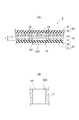
本実施形態では、図1(A)及び図1(B)に示すように、樹脂付銅箔10の樹脂層11において屈曲部1aに対応する部分に低剛性部12Aが形成されている。
In this embodiment, as shown to FIG. 1 (A) and FIG. 1 (B), low-
この低剛性部12Aは、樹脂層11に形成した凹部121を有している。この低剛性部12Aの層厚t1は、樹脂層11における他の部分の層厚t0よりも相対的に薄くなっており(t1<t0)、この低剛性部12Aは、樹脂層11における他の部分よりも剛性が低くなっている。また、この低剛性部12Aでは、樹脂層11を完全に除去せずに若干の厚さの樹脂層11を残存させているので、この低剛性部12A上にも配線パターン16を形成することが可能となっている。
The low rigidity portion 12 </ b> A has a
なお、この低剛性部は、樹脂層においてその他の部分よりも剛性が低ければ、その形状は特に限定されない。 The shape of the low rigidity portion is not particularly limited as long as the rigidity is lower than that of other portions in the resin layer.
図2(A)及び図2(B)は本実施形態における多層配線板の第1変形例を示す図である。同図に示すように、低剛性部12Bが、樹脂層11に形成した多数のスリット122を有してもよい。この場合にも、低剛性部12Bの層厚t2が、樹脂層11における他の部分の層厚t0よりも部分的に薄くなっており(t2<t0)、低剛性部12Bは、樹脂層11における他の部分よりも剛性が低くなっている。
2A and 2B are views showing a first modification of the multilayer wiring board in the present embodiment. As shown in the figure, the low-rigidity portion 12 </ b> B may have a large number of
また、図3は本実施形態における多層配線板の第2変形例の低剛性部を示す図である。同図に示すように、凹部121や多数のスリット122に代えて、低剛性部12Cが、樹脂層11に形成した多数の穴123を有してもよい。この場合にも、特に図示しないが、低剛性部12Cの層厚が、樹脂層11における他の部分の層厚よりも部分的に薄くなっており、低剛性部12Cは、樹脂層11における他の部分よりも剛性が低くなっている。なお、図3は、図1(B)や図2(B)と同じ視点から低剛性部12Cを見た図である。
FIG. 3 is a view showing a low-rigidity portion of a second modification of the multilayer wiring board in the present embodiment. As shown in the figure, the low-rigidity portion 12 </ b> C may have a large number of
図4は本実施形態における多層配線板の第3変形例の低剛性部を示す図である。同図に示すように、低剛性部12Dの凹部121のコーナ部124を曲線状にしてもよい。これにより、多層配線板1を屈曲部1aで曲げたときに凹部121のコーナ部124に集中する応力を緩和することができる。なお、図4は、第3変形例の多層配線板において、図1(A)の符号1aで示す一点鎖線で囲まれた領域と同じ領域を示す図である。
FIG. 4 is a view showing a low-rigidity portion of a third modification of the multilayer wiring board in the present embodiment. As shown in the figure, the
図1(A)に戻り、銅張積層板20は、絶縁性基板21と、当該絶縁性基板21上に形成された配線パターン26とを有している。なお、銅張積層板20として、絶縁性基板21の両面に銅箔25を貼り付けたもの(いわゆる両面銅張積層板)を用いてもよい。また、銅張積層板20として、絶縁性基板と配線パターンとの間に接着層が介在している銅張積層板を用いてもよい。
Returning to FIG. 1A, the copper-clad
絶縁性基板21は、電気絶縁性及び可撓性を有する樹脂フィルムから構成されている。この絶縁性基板21を構成する具体的な材料としては、例えば、ポリイミド(PI)、ポリエステル(PE)、ガラスエポキシ樹脂等を例示することができる。なお、このフレキシブルな絶縁性基板21に代えて、例えば、ガラスエポキシ樹脂、セラミックス、ガラスなどのリジッドな絶縁性基板を用いてもよい。
The insulating
配線パターン26は、絶縁性基板21に貼り付けられた銅箔25(図9(A)参照)に対してエッチング処理等を施すことで形成されている。なお、銅張積層板20の金属箔として、銅箔25に代えて、例えば、アルミニウム箔や銀箔等を用いてもよい。
The
以上に説明した樹脂付銅箔10は、樹脂付銅箔10の樹脂層11と銅張積層板20の配線パターン26とが重なるように、銅張積層板20の上に貼り付けられており、Bステージ状態の樹脂層11を加熱して硬化させることで、樹脂付銅箔10と銅張積層板20とが接着されている。この際、図1(A)に示すように、低剛性部12Aの凹部121が銅張積層板20に覆われるので、樹脂付銅箔10と銅張積層板20との間に中空部が形成される。なお、Bステージとは、樹脂が流動状のワニス状態にあるAステージと、樹脂が完全に硬化した状態にあるCステージと、の間の段階であり、硬化反応の中間段階のことである。
The copper foil with
なお、銅張積層板20の形状は特に限定されず、例えば、図5や図6に示す変形例のように、銅張積層板20に開口27や切欠28を形成してもよい。
The shape of the copper clad
図5は本実施形態における多層配線板の第4変形例を示す断面図である。同図に示すように、銅張積層板20において低剛性部12Aに対向する部分に開口27を形成して、当該開口27を介して低剛性部12Aを銅張積層板20から露出させてもよい。これにより、屈曲部1aでの多層配線板1の屈曲性を向上させることができる。
FIG. 5 is a cross-sectional view showing a fourth modification of the multilayer wiring board in the present embodiment. As shown in the figure, an
図6は本実施形態における多層配線板の第5変形例を示す断面図である。同図に示すように、低剛性部12Aを樹脂付銅箔10の端部に形成すると共に、銅張積層板20の端部に切欠28を形成することで、多層配線板1の端部をフライングテール構造としてもよい。切欠28は、銅張積層板20において樹脂付銅箔10の低剛性部12Aに対応する部分に形成されており、樹脂付銅箔10の低剛性部12Aは、切欠28を介して銅張積層板20から露出している。これにより、屈曲部1aでの多層配線板1の屈曲性を向上させることができる。
FIG. 6 is a cross-sectional view showing a fifth modification of the multilayer wiring board in the present embodiment. As shown in the figure, the low-
また、図7に示すように、樹脂付銅箔10と銅張積層板20との間に中空部を形成しなくてもよい。図7は本実施形態における多層配線板の第6変形例を示す断面図である。同図に示すように、樹脂付銅箔10を銅箔付絶縁性基板20に貼り付ける際に、低剛性部12Aの凹部121を押し潰すことで、中空部を形成せずに樹脂付銅箔10と銅張積層板20とを密着させてもよい。
Further, as shown in FIG. 7, it is not necessary to form a hollow portion between the resin-coated
図1(A)に戻り、銅張積層板20に貼り付けられた樹脂付銅箔10の上面には、カバーレイ30(CL:Coverlay)が積層されている。このカバーレイ30は、樹脂付銅箔10の配線パターン16を保護する樹脂層31と、当該樹脂層31を樹脂付銅箔10に貼り付ける接着層32と、を有している。
Returning to FIG. 1A, a cover lay 30 (CL: Coverlay) is laminated on the upper surface of the resin-coated
カバーレイ30の樹脂層31は、例えば、ポリイミドから構成されている。また、カバーレイ30の接着層32は、例えば、エポキシ系樹脂やアクリル系樹脂からなる接着剤で構成されている。
The
なお、ポリエステル、エポキシ、アクリル、ポリイミド、ポリウレタン等を用いた感光性カバーレイ材料からなるドライフィルムで樹脂層31を構成してもよい。或いは、ポリイミドやエポキシをベースとしたカバーインクや液状の感光性カバーレイ材料を、樹脂付銅箔10上にスクリーン印刷することで、カバーレイ30を形成してもよい。
In addition, you may comprise the
一般的に、樹脂付銅箔はフレキシブルプリント配線板よりも低コストであるが、樹脂付銅箔の樹脂層がフレキシブルプリント配線板のベースフィルムと比較して柔軟性に劣るため、多層配線板の屈曲部には不向きである。 Generally, resin-coated copper foil is less expensive than flexible printed wiring boards, but the resin layer of resin-coated copper foil is less flexible than the base film of flexible printed wiring boards. It is not suitable for the bent part.
これに対し、本実施形態では、樹脂付銅箔10の樹脂層11において屈曲部1aに対応する部分に、樹脂層11のその他の部分よりも相対的に剛性の低い低剛性部12Aを形成するので、多層配線板1の屈曲部1aに樹脂付銅箔10を使用することができる。これにより、多層配線板1のコスト低減を図ることができる。
In contrast, in the present embodiment, a low-
一方、樹脂層11における低剛性部12A以外の部分は、銅箔積層板20の配線パターン26を保護するのに十分な層厚t0を有しているので、信頼性を損なうことがない。従って、本実施形態の樹脂付銅箔10では、屈曲性と信頼性の両立を実現することができる。
On the other hand, portions other than the
以下に、本実施形態における多層配線板1の製造方法について、図8及び図9を参照しながら説明する。図8は本実施形態における多層配線板の製造方法を示すフローチャート、図9(A)〜図9(E)は図8の各ステップにおける多層配線板を示す断面図である。
Below, the manufacturing method of the
先ず、図8のステップS10において、図9(A)に示すように、銅張積層板20上に配線パターン26をサブトラクティブ法によって形成する。具体的には、銅張積層板20の銅箔25上に、配線パターン26に対応した形状のマスクを用いてレジストパターンを形成し、その後、塩化鉄エッチング液、塩化銅エッチング液又はアルカリエッチャント等を用いて銅箔に対してエッチング処理を行う。これにより、銅張積層板20上に配線パターン26が形成される。
First, in step S10 of FIG. 8, as shown in FIG. 9A, the
次いで、図8のステップS20において、図9(B)に示すように、インプリント法によって、樹脂付銅箔10の樹脂層11に低剛性部12Aを形成する。
Next, in step S20 of FIG. 8, as shown in FIG. 9B, a low-
具体的には、先ず、低剛性部12Aの凹部121に対応した形状の凸部101を有するモールド100を準備する。このモールド100を構成する材料としては、例えば、石英、シリコン(Si)、シリコンカーバイト(SiC)、グラッシーカーボン(GC)、ニッケル(Ni)、タンタル(Ta)、ステンレス、プラスチック等を例示することができる。なお、離型性を向上させるために、モールド100の表面全体にフッ素コーティング等の表面処理を施してもよい。
Specifically, first, a
次いで、当該凸部101を樹脂層11において凹部121を形成すべき部位に対向させて、モールド100を樹脂層11に押し付ける。この際、モールド100の凸部101は、樹脂層11が硬化する程度の温度に加熱されているので、当該押圧及び加熱によって、凸部101の形状が樹脂層11に転写されて、当該樹脂層11に凹部121が形成される。
Next, the
また、モールド100が加熱されていることから、押圧時に凹部121の表面で硬化が進行する。このため、本実施形態では、樹脂付銅箔10と銅箔付絶縁性基板20との貼り合わせ時の凹部121の変形を抑制したり、貼り合わせ後も凹部121の形状を維持することができる。
Further, since the
なお、低剛性部12Aの形成方法は特に上記に限定されず、以下の方法を用いてもよい。図10(A)及び図10(B)は本実施形態における低剛性部の形成方法の変形例を示す図である。 In addition, the formation method of 12 A of low rigidity parts is not specifically limited above, You may use the following method. FIG. 10A and FIG. 10B are diagrams showing a modification of the method for forming the low-rigidity portion in the present embodiment.
先ず、図10(A)に示すように、樹脂付銅箔10の樹脂層11の表面に保護フィルム120を積層する。この保護フィルム120は、例えばポリエチレンから構成されており、樹脂層11において低剛性部12Aを形成すべき硬化対象部位11aに対応する部分に開口120aが形成されている。なお、本実施形態における硬化対象部位11aが、本発明における樹脂層の所定部位の一例に相当する。
First, as shown to FIG. 10 (A), the
さらに、この保護フィルム120の上に、冷却ジャケット130を積層する。この冷却ジャケット130は、例えば、冷媒が流通可能な流路131が内部に形成された板状部材であり、保護フィルム120の開口120aと同一位置に開口132が形成されている。冷却ジャケット130の流路131は、配管を介してチラー133に接続されており、この冷却ジャケット130は、樹脂層11における硬化対象部位11a以外の部分を後述のヒータ110の熱から保護すると共に、保護フィルム120を介して樹脂層11を冷却することが可能となっている。なお、冷却ジャケット130の構成は、樹脂層11における硬化対象部位11a以外の部分をヒータ110の熱から保護するものであれば、上記のものに限定されない。
Further, a cooling
そして、図10(A)に示すように、樹脂付金属箔10の樹脂層11をヒータ110で加熱する。ヒータ110の熱は、冷却ジャケット130及び保護フィルム120の開口132,120aを介して、樹脂層11の硬化対象部位11aに伝わり、この熱によって樹脂層11の硬化対象部位11aが硬化する。
Then, as shown in FIG. 10A, the
なお、図10(A)に示すように、それぞれの開口120a,132の幅w1は、樹脂層11における熱の広がりを考慮して、樹脂層11における硬化対象部位11aの幅w2よりも若干狭く設定されている(w1<w2)。一方、図10(B)に示すように、樹脂層11における硬化対象部位11aの幅w2は、凹部121の幅w3よりも若干広めに設定されている(w2>w3)。
As shown in FIG. 10A, the width w 1 of each of the
次いで、図10(B)に示すように、樹脂層11において冷却ジャケット130及び保護フィルム120の開口132,120aから露出している部分に向かって、レーザ照射装置140からレーザ光Lを照射しながら当該レーザ照射装置140を走査させることで、樹脂層11に凹部121を形成する。
Next, as shown in FIG. 10B, while irradiating the laser beam L from the
なお、レーザ加工に代えて、プラズマを用いたドライエッチングによって樹脂層11を選択的に除去することで、樹脂層11に凹部121を形成してもよい。この場合には、エッチング処理に際して、樹脂層11において凹部121を形成する部分以外の表面にエッチングレジストを形成しておく。
Note that the
また、レーザ加工に代えて、デスミア加工を応用して、例えば過マンガン酸塩によって樹脂層11を部分的に溶融させることで、樹脂層11に凹部121を形成してもよい。
Moreover, it may replace with laser processing and you may form the recessed
これらの変形例では、樹脂層11の硬化対象部位11aを事前に硬化させておくことで、レーザ加工、エッチング加工、或いはデスミア加工によって低剛性部12Aを正確に形成することが可能となっている。
In these modified examples, by curing the
また、低剛性部12Aが硬化しているので、樹脂付銅箔10と銅箔付絶縁性基板20との貼り合わせ時の凹部121の変形を抑制したり、貼り合わせ後も凹部121の形状を維持することができる。
In addition, since the low-
なお、レーザ加工によって樹脂層11の硬化対象部位11aを硬化温度まで加熱することが可能である場合には、ヒータによる樹脂層11の加熱は不要である。
In addition, when it is possible to heat the hardening object site |
図8に戻り、次いで、ステップS30において、図9(C)に示すように、樹脂付銅箔10の樹脂層11が、銅張積層板20において配線パターン26が形成された面に重なるように、銅張積層板20の上に樹脂付銅箔10を貼り合わせる。この際、樹脂付銅箔10と銅張積層板20を加熱しながらプレスすることで、Bステージ状態であった樹脂層11は、一度溶融した後に完全に硬化する。これにより、樹脂層11を介して、樹脂付銅箔10と銅張積層板20とが接着される。
Returning to FIG. 8, next, in step S <b> 30, as shown in FIG. 9C, the
次いで、図8のステップS40において、図9(D)に示すように、銅張積層板20の配線パターン26と同様の要領で、樹脂付銅箔10上に配線パターン16をサブトラクティブ法によって形成する。
Next, in step S40 of FIG. 8, as shown in FIG. 9D, the
次いで、図8のステップS50において、図9(E)に示すように、樹脂付銅箔10上にカバーレイ30を貼り合わせて、これらを加熱しながらプレスすることで、接着層32によってカバーレイ30と樹脂付銅箔10とを接着する。
Next, in step S50 of FIG. 8, as shown in FIG. 9E, the cover lay 30 is bonded onto the resin-coated
なお、以上に説明したステップS10〜S50の順序は、上記に限定されない。例えば、ステップS20をステップS10よりも先に実施してもよく、ステップS10とステップS20の先後は問わない。また、ステップS40は、ステップS50よりも先であれば、ステップS10、S20或いはS30よりも先であってもよい。 The order of steps S10 to S50 described above is not limited to the above. For example, step S20 may be performed before step S10, and the order after step S10 and step S20 does not matter. Further, step S40 may be ahead of step S10, S20 or S30 as long as it is ahead of step S50.
以上のように、本実施形態では、樹脂付銅箔10の樹脂層11において屈曲部1aに対応する部分に、樹脂層11のその他の部分よりも相対的に剛性の低い低剛性部12Aを形成するので、低コストな樹脂付銅箔10を多層配線板1の屈曲部1aに使用することができる。
As described above, in the present embodiment, the low-rigidity portion 12 </ b> A having lower rigidity than the other portions of the
また、インプリント法によって低剛性部12Aを形成することで、樹脂部11に凹部121を形成すると同時に低剛性部12Aの表面を硬化させることもできるので、低剛性部12Aを有する多層配線板1の製造工程が簡素化される。
Moreover, since the surface of the low-
なお、以上に説明した実施形態は、本発明の理解を容易にするために記載されたものであって、本発明を限定するために記載されたものではない。したがって、上記の実施形態に開示された各要素は、本発明の技術的範囲に属する全ての設計変更や均等物をも含む趣旨である。 The embodiment described above is described for facilitating the understanding of the present invention, and is not described for limiting the present invention. Therefore, each element disclosed in the above embodiment is intended to include all design changes and equivalents belonging to the technical scope of the present invention.
1…多層配線板
1a…屈曲部
10…樹脂付銅箔
11…樹脂層
12A,12B,12C,12D…低剛性部
121…凹部
15…銅箔
16…配線パターン
20…銅張積層板
21…絶縁性基板
25…銅箔
26…配線パターン
30…カバーレイ
100…モールド
101…凸部
110…ヒータ
120…保護フィルム
130…冷却ジャケット
140…レーザ照射装置
DESCRIPTION OF
Claims (10)
前記金属箔付絶縁性基板に第1の配線パターンを形成する第1のステップと、
前記樹脂付金属箔の樹脂層に低剛性部を形成する第2のステップと、
前記樹脂付金属箔の前記樹脂層を、前記金属箔付絶縁性基板において前記第1の配線パターンが形成された面に貼り合わせる第3のステップと、
前記樹脂付金属箔に第2の配線パターンを形成する第4のステップと、を備えており、
前記低剛性部の少なくとも一部は、前記樹脂層における他の部分よりも相対的に薄肉であることを特徴とする多層配線板の製造方法。 A method for producing a multilayer wiring board comprising a laminated metal foil with resin and an insulating substrate with metal foil,
A first step of forming a first wiring pattern on the insulating substrate with metal foil;
A second step of forming a low rigidity portion in the resin layer of the metal foil with resin;
A third step of bonding the resin layer of the metal foil with resin to the surface on which the first wiring pattern is formed on the insulating substrate with metal foil;
A fourth step of forming a second wiring pattern on the resin-coated metal foil,
At least a part of the low-rigidity part is relatively thinner than other parts in the resin layer.
前記第2のステップは、インプリント法によって、前記低剛性部を前記樹脂層に形成すると同時に前記低剛性部の表面を加熱して硬化させることを含むことを特徴とする多層配線板の製造方法。 It is a manufacturing method of the multilayer wiring board according to claim 1,
The second step includes forming the low-rigidity portion on the resin layer by an imprint method, and simultaneously heating and curing the surface of the low-rigidity portion. .
前記第2のステップは、前記樹脂層の所定部位を加熱して硬化させた後に前記所定部位に前記低剛性部を形成することを含むことを特徴とする多層配線板の製造方法。 It is a manufacturing method of the multilayer wiring board according to claim 1,
The method of manufacturing a multilayer wiring board, wherein the second step includes forming the low-rigidity portion at the predetermined portion after the predetermined portion of the resin layer is heated and cured.
前記低剛性部は、前記樹脂層に形成された凹部、複数のスリット、又は複数の穴を有することを特徴とする多層配線板の製造方法。 A method for producing a multilayer wiring board according to any one of claims 1 to 3,
The method of manufacturing a multilayer wiring board, wherein the low-rigidity part has a recess, a plurality of slits, or a plurality of holes formed in the resin layer.
前記低剛性部の隅部は、曲線状の断面形状を有することを特徴とする多層配線板の製造方法。 A method for producing a multilayer wiring board according to any one of claims 1 to 4,
The method of manufacturing a multilayer wiring board, wherein the corner portion of the low-rigidity portion has a curved cross-sectional shape.
前記金属箔付絶縁性基板は、
絶縁性基板と、
前記絶縁性基板上に形成された第1の配線パターンと、を有し、
前記樹脂付金属箔は、
低剛性部を有する樹脂層と、
前記樹脂層上に形成された第2の配線パターンと、を有し、
前記樹脂付金属箔の前記樹脂層が、前記金属箔付絶縁性基板において前記第1の配線パターンが形成された面に貼り付けられており、
前記低剛性部の少なくとも一部は、前記樹脂層における他の部分よりも相対的に薄肉であることを特徴とする多層配線板。 A multilayer wiring board configured by laminating a metal foil with resin and an insulating substrate with metal foil,
The insulating substrate with metal foil is
An insulating substrate;
A first wiring pattern formed on the insulating substrate,
The metal foil with resin is
A resin layer having a low rigidity portion;
A second wiring pattern formed on the resin layer,
The resin layer of the metal foil with resin is attached to the surface on which the first wiring pattern is formed on the insulating substrate with metal foil,
At least a part of the low-rigidity part is thinner than other parts in the resin layer.
前記金属箔付絶縁性基板は、前記低剛性部に対向する部分を有しており、
前記低剛性部によって前記樹脂付金属箔と前記金属箔付絶縁性基板との間に中空部が形成されていることを特徴とする多層配線板。 The multilayer wiring board according to claim 6,
The insulating substrate with metal foil has a portion facing the low rigidity portion,
A multilayer wiring board, wherein a hollow portion is formed between the metal foil with resin and the insulating substrate with metal foil by the low rigidity portion.
前記低剛性部は、前記金属箔付絶縁性基板から露出していることを特徴とする多層配線板。 The multilayer wiring board according to claim 6,
The multilayer wiring board, wherein the low rigidity portion is exposed from the insulating substrate with metal foil.
前記低剛性部は、前記樹脂層に形成された凹部、複数のスリット、又は複数の穴を有することを特徴とする多層配線板。 A multilayer wiring board according to any one of claims 6 to 8,
The low-rigidity portion has a recess, a plurality of slits, or a plurality of holes formed in the resin layer.
前記低剛性部の隅部は、曲線状の断面形状を有することを特徴とする多層配線板。 A multilayer wiring board according to any one of claims 6 to 9,
A corner of the low-rigidity portion has a curved cross-sectional shape.
Priority Applications (1)
| Application Number | Priority Date | Filing Date | Title |
|---|---|---|---|
| JP2010249423A JP2012104530A (en) | 2010-11-08 | 2010-11-08 | Manufacturing method of multilayer wiring board and multilayer wiring board |
Applications Claiming Priority (1)
| Application Number | Priority Date | Filing Date | Title |
|---|---|---|---|
| JP2010249423A JP2012104530A (en) | 2010-11-08 | 2010-11-08 | Manufacturing method of multilayer wiring board and multilayer wiring board |
Publications (1)
| Publication Number | Publication Date |
|---|---|
| JP2012104530A true JP2012104530A (en) | 2012-05-31 |
Family
ID=46394628
Family Applications (1)
| Application Number | Title | Priority Date | Filing Date |
|---|---|---|---|
| JP2010249423A Pending JP2012104530A (en) | 2010-11-08 | 2010-11-08 | Manufacturing method of multilayer wiring board and multilayer wiring board |
Country Status (1)
| Country | Link |
|---|---|
| JP (1) | JP2012104530A (en) |
-
2010
- 2010-11-08 JP JP2010249423A patent/JP2012104530A/en active Pending
Similar Documents
| Publication | Publication Date | Title |
|---|---|---|
| JP6416093B2 (en) | Manufacturing method of flexible printed wiring board | |
| KR101156751B1 (en) | Flex-rigid printed circuit board, and method for manufacturing the flex-rigid printed circuit board | |
| KR101098072B1 (en) | Flexible wiring board and method of manufacturing same | |
| TW201124027A (en) | Carrier for manufacturing substrate and method of manufacturing substrate using the same | |
| KR20130079197A (en) | Multilayer wiring substrate and method of manufacturing the same | |
| TW201501582A (en) | Build-up material for use in printed-circuit board and applications thereof, printed-circuit board having inner buried elements | |
| JP2007142188A (en) | Multilayer printed wiring board and manufacturing method thereof | |
| JP2009302343A (en) | Multilayer substrate, and method of manufacturing the same | |
| JP6342357B2 (en) | Printed circuit board and manufacturing method thereof | |
| JP2012104530A (en) | Manufacturing method of multilayer wiring board and multilayer wiring board | |
| JP2006066738A (en) | Multi-layer printed wiring board, copper-clad laminate therefor, and method for manufacturing the same | |
| JP2007129153A (en) | Rigid flex multilayer printed wiring board | |
| JP2006228887A (en) | Manufacturing method of rigid-flex multilayer printed wiring board | |
| JP2010010488A (en) | Manufacturing method of wiring board, and wiring board | |
| JP2007188986A (en) | Multilayer circuit board and manufacturing method thereof | |
| KR20110070158A (en) | Manufacturing Method of FPCB Using Bonding Sheet | |
| JP5050505B2 (en) | Multilayer printed wiring board manufacturing method and printed wiring board | |
| JP2006294666A (en) | Flex rigid wiring board and manufacturing method thereof | |
| CN115942636B (en) | Circuit board processing method and circuit board | |
| JPH0493093A (en) | Forming method for electronic component containing recess of circuit board | |
| JP5123145B2 (en) | Flex rigid printed circuit board | |
| JP2011108826A (en) | Manufacturing method of multilayer printed wiring board, and the multilayer printed wiring board manufactured by using the manufacturing method | |
| JP2012169523A (en) | Manufacturing method of rigid flexible printed wiring board | |
| CN101730388B (en) | Circuit board and manufacturing method thereof | |
| JP2010129610A (en) | Flex-rigid printed wiring board |