JP2012104017A - Electrostatic input device - Google Patents
Electrostatic input device Download PDFInfo
- Publication number
- JP2012104017A JP2012104017A JP2010253695A JP2010253695A JP2012104017A JP 2012104017 A JP2012104017 A JP 2012104017A JP 2010253695 A JP2010253695 A JP 2010253695A JP 2010253695 A JP2010253695 A JP 2010253695A JP 2012104017 A JP2012104017 A JP 2012104017A
- Authority
- JP
- Japan
- Prior art keywords
- detection
- contact
- electrode
- touch
- touch electrode
- Prior art date
- Legal status (The legal status is an assumption and is not a legal conclusion. Google has not performed a legal analysis and makes no representation as to the accuracy of the status listed.)
- Pending
Links
Images


Abstract
Description
本発明は、静電入力装置に関する。 The present invention relates to an electrostatic input device.
従来、スライド操作量を検出してその方向と操作量を入力するスライド入力装置として、光学式、抵抗膜式等の種々のものが提案され使用されている。例えば、直線または平面曲線もしくは空間曲線状の所定の軌跡上に連続して複数のタッチ検出センサーを配したタッチ検知手段を有す入力装置において、軌跡上を倣って繰り返しタッチ入力される長さと方向とを取り込む手段を持つタッチ入力検知装置がある(例えば、特許文献1参照)。 Conventionally, various types of slide input devices such as an optical type and a resistive film type have been proposed and used as a slide input device that detects a slide operation amount and inputs the direction and the operation amount. For example, in an input device having touch detection means in which a plurality of touch detection sensors are continuously arranged on a predetermined locus of a straight line, a plane curve, or a space curve, the length and direction in which touch input is repeated following the locus There is a touch input detection device having a means for capturing (see, for example, Patent Document 1).
このタッチ入力検知装置によれば、複数のタッチ検出センサーにより、連続した多くの項目、データが検出可能であり、これを使用して多くの機能やデータの選択を行ったり、多くの機能を簡単に利用することが出来る電子機器等を構成することが可能になるとされている。 According to this touch input detection device, a number of continuous items and data can be detected by a plurality of touch detection sensors, and many functions and data can be selected using this, and many functions can be easily performed. It is said that it is possible to configure an electronic device that can be used for the same.
また、所定領域を占める薄膜状に形成されている一つの電極と、その電極と接続されてこの電極に向けて帯電された帯電体を接近または接触させることで、その帯電体と電極との間で生じる静電容量に応じた出力信号を出力する出力手段とを備えた入力装置がある(例えば、特許文献2参照)。 In addition, a single electrode formed in a thin film occupying a predetermined area and a charged body connected to the electrode and charged toward the electrode are brought close to or in contact with each other, so that there is a gap between the charged body and the electrode. There is an input device provided with output means for outputting an output signal corresponding to the capacitance generated in (see, for example, Patent Document 2).
この装置は、電極が所定方向に延出し、その所定方向に延出する両縁部の間隔が第1の幅で形成される第1の領域と、その第1の領域の第1の幅よりも長い又は短い第2の幅で形成される第2の領域とを有するように形成されており、出力手段によって出力される出力信号が示す出力値の変化を調査する調査手段と、その調査手段による調査結果に応じて、電極が延出する所定方向に向けて帯電体を電極に対して接近または接触させた状態でスライドさせる操作がされたのかを特定する特定手段とを備える。このタッチ入力装置によれば、簡単な構成で、スライド操作がされたのかを特定することができるとされている。 In this device, an electrode extends in a predetermined direction, and a first region in which a distance between both edges extending in the predetermined direction is formed with a first width, and a first width of the first region. Survey means for investigating the change in the output value indicated by the output signal output by the output means, and the survey means And a specifying unit that specifies whether an operation of sliding the charged body in a state of approaching or contacting the electrode in a predetermined direction in which the electrode extends is performed in accordance with the investigation result. According to this touch input device, it is said that it is possible to specify whether the slide operation has been performed with a simple configuration.
しかし、特許文献1に記載のタッチ入力検知装置は、複数のタッチ検出センサを多数連続して配置した構成とする必要がある。このため、静電検出回路の規模が大きくなり、電極と回路の接続線数が多くなりコスト高になるという問題もあった。また、特許文献2に記載の入力装置は、1つの電極でスライド操作の方向を検出することができるが、帯電体が電極に対して接触した状態でスライド操作されたのかの判断がなされず、検出精度が低いと共に、位置検出ができないという問題もあった。
However, the touch input detection device described in
従って、本発明の目的は、少ない検出電極数でスライド方向および位置の検出を可能とする静電入力装置を提供することにある。 Accordingly, an object of the present invention is to provide an electrostatic input device that can detect the sliding direction and position with a small number of detection electrodes.
[1]本発明は、上記目的を達成するため、入力接触面上または前記入力接触面に沿って設けられ、長尺状に形成された第1の電極と、前記第1の電極から離間して設けられ、長尺状に形成された第2の電極と、前記第1の電極への検出対象物の近接または接触により前記第1の電極から検出される静電容量、及び、前記第2の電極から検出される静電容量に基づいて、前記検出対象物の操作方向または操作位置を検出する検出制御部と、を有することを特徴とする静電入力装置を提供する。 [1] In order to achieve the above object, the present invention provides a first electrode formed on the input contact surface or along the input contact surface and formed in an elongated shape, and is separated from the first electrode. A second electrode formed in a long shape, a capacitance detected from the first electrode by the proximity or contact of an object to be detected to the first electrode, and the second And a detection control unit that detects an operation direction or an operation position of the detection object based on a capacitance detected from the electrodes of the electrostatic input device.
[2]前記第2の電極は、前記検出対象物が前記入力接触面上の異なる位置に近接または接触したときに、異なる静電容量値を検出するように、前記入力接触面に対して傾斜して形成されていることを特徴とする上記[1]に記載の静電入力装置であってもよい。 [2] The second electrode is inclined with respect to the input contact surface so as to detect different capacitance values when the detection object approaches or comes into contact with a different position on the input contact surface. The electrostatic input device according to the above [1] may be formed.
[3]また、前記第1の電極、及び、前記第2の電極は、前記入力接触面の法線方向に投影した状態で、互いに重ならずに所定の間隔を有して配置されていることを特徴とする上記[1]又は[2]に記載の静電入力装置であってもよい。 [3] Further, the first electrode and the second electrode are arranged with a predetermined interval without overlapping each other in a state projected in the normal direction of the input contact surface. The electrostatic input device according to the above [1] or [2] may be used.
本発明の一形態によれば、少ない検出電極数でスライド方向および位置の検出を可能とする静電入力装置を提供することができる。 According to one embodiment of the present invention, it is possible to provide an electrostatic input device that enables detection of a sliding direction and a position with a small number of detection electrodes.
(本発明の第1の実施の形態に係る静電入力装置)
図1は、本発明の第1の実施の形態に係る静電入力装置全体の概略構成図である。静電入力装置10は、ベースパネル200、ベースパネル200の上面に操作者の手指等でスライド入力操作される方向に長尺状に形成された接触検出用タッチ電極100、及び、ベースパネル200の下面に操作者の手指等でスライド入力操作される方向に長尺状に形成されたスライド操作検出用タッチ電極150とを有して構成される入力センサ部50と、接触検出用タッチ電極100への検出対象物の近接または接触により接触検出用タッチ電極100から検出される静電容量、及び、スライド操作検出用タッチ電極150から検出される静電容量に基づいて、検出対象物の操作方向または操作位置を検出する検出制御部480とから概略構成されている。
(Electrostatic input device according to the first embodiment of the present invention)
FIG. 1 is a schematic configuration diagram of the entire electrostatic input device according to the first embodiment of the present invention. The electrostatic input device 10 includes a
図2(a)は、本発明の第1の実施の形態に係る静電入力装置10の入力センサ部の全体斜視図であり、図2(b)は、入力センサ部を上方向からみた上平面図である。 2A is an overall perspective view of the input sensor unit of the electrostatic input device 10 according to the first embodiment of the present invention, and FIG. 2B is a top view of the input sensor unit viewed from above. It is a top view.
第1の電極である接触検出用タッチ電極100は、導電性材料、例えば、銅系材料による薄膜の長尺状に形成されたパターンであって、後述するベースパネル200の上面に配置されている。この接触検出用タッチ電極100は、ベースパネル200の入力接触面であるベース上面200aに配置されていることから、検出対象物、例えば、操作者の手指が接触または近接することができる。また、長尺状に形成されているので、操作者の手指がその長尺方向に操作されることで連続的にあるいは断続的にスライド入力することができる。
The
第2の電極であるスライド操作検出用タッチ電極150は、接触検出用タッチ電極100と同様に、導電性材料、例えば、銅系材料による薄膜の長尺状に形成されたパターンであって、接触検出用タッチ電極100から離間してベースパネル200の下面に配置されている。スライド操作検出用タッチ電極150は、操作者の手指がベースパネル200のベース上面200aの異なる位置に近接または接触したときに、異なる静電容量値を検出するように、ベース上面200aに対して傾斜して形成されている。詳細は後述するが、スライド操作時に、操作者の手指とスライド操作検出用タッチ電極150との間の距離がスライド方向(長尺方向)に漸次変化するように形成されている。
The
ベースパネル200は、接触検出用タッチ電極100及びスライド操作検出用タッチ電極150を支持固定するためのものである。接触検出用タッチ電極100を支持するベース上面200aに対してベース下面200bは所定の角度で傾斜して形成されている。このベースパネル200は、誘電体であり、例えば、ポリカーボネート(PC)等の樹脂で形成され、このPCの場合は、比誘電率εrが約3である。
The
ここで、図2(b)に示す接触検出用タッチ電極100の幅H1及びスライド操作検出用タッチ電極150の幅H2は、略同一とされている。この接触検出用タッチ電極100とスライド操作検出用タッチ電極150は、ベース上面200aの法線方向(Nベクトル)に投影した状態で、図2(b)に示すように、互いに重ならずに所定の間隔W1を有して配置されている。これにより、少なくとも対向面積が干渉しない構成とすることができる。
Here, the width H1 of the touch electrode for
また、ベース上面200aには、スライド操作の案内として、例えば図2(a)、(b)に示すような意匠マーク220である矢印が形成されている。意匠マーク220は、非導電性材料により印刷等で形成されている。この矢印に従ってスライド等の操作を行なうと、手指が接触検出用タッチ電極100とスライド操作検出用タッチ電極150との間に接触または近接する。これにより、手指とスライド操作検出用タッチ電極150との間の静電容量が安定し、かつ、検出に十分な静電容量が確保される。尚、意匠マーク220は、接触検出用タッチ電極100とスライド操作検出用タッチ電極150に略等しい割合で跨ってベース上面200a上に形成されていることが好ましい。また、意匠マーク220の幅W2は、手指とベース上面200aとの接触面積と同程度にすることが好ましい。
In addition, an arrow that is a
図3は、図2で示した入力センサ部の変形例を示す図2(a)相当の全体斜視図である。ベースパネル200の下部に支持パネル210を設け、ベース上面200aが略水平になるようにすることで、入力センサ部50を載置した状態で操作者が手指でベース上面200aをスライド等の操作を行ないやすいようにすることができる。
FIG. 3 is an overall perspective view corresponding to FIG. 2A showing a modification of the input sensor unit shown in FIG. The
検出制御部480は、スライド容量検出部481、接触容量検出部482、スライド入力位置判定部483、接触判定部484、通信制御部485から構成されている。この検出制御部480には、接触検出用タッチ電極100及びスライド操作検出用タッチ電極150からの検出信号Vs1、Vs2が入力される。ここで、図1により、静電入力装置10の回路構成を説明する。
The detection control unit 480 includes a slide
図1において、交流信号を出力する発振器400Aは、この発振器400Aから出力された交流信号を増幅するアンプ410Aとアンプ410Aによって増幅された交流信号を調整する負荷抵抗420Aを介して直列に接触検出用タッチ電極100の一端に接続されている。また、接触検出用タッチ電極100の一端は、上記した負荷抵抗420Aの一端に接続されると共に、交流信号を増幅するアンプ430Aと、所定の周波数のみを通過させてノイズを除去するBPF(Band-Pass-Filter)440Aと、交流信号を整流するダイオード等からなる整流器450Aと、整流された整流信号をDC信号にするLPF(Low-Pass-Filter)460Aに直列に接続されている。これにより、接触検出用タッチ電極100へのタッチ信号が検出信号Vs1として検出制御部480に入力される。
In FIG. 1, an oscillator 400A that outputs an AC signal is used for contact detection in series via an amplifier 410A that amplifies the AC signal output from the oscillator 400A and a load resistor 420A that adjusts the AC signal amplified by the amplifier 410A. It is connected to one end of the
スライド操作検出用タッチ電極150も同様に、交流信号を出力する発振器400Bから出力された交流信号を増幅するアンプ410Bとアンプ410Bによって増幅された交流信号を調整する負荷抵抗420Bを介して直列にスライド操作検出用タッチ電極150の一端に接続されている。また、スライド操作検出用タッチ電極150の一端は、上記した負荷抵抗420Bの一端に接続されると共に、交流信号を増幅するアンプ430Bと、所定の周波数のみを通過させてノイズを除去するBPF(Band-Pass-Filter)440Bと、交流信号を整流するダイオード等からなる整流器450Bと、整流された整流信号をDC信号にするLPF(Low-Pass-Filter)460Bに直列に接続されている。これにより、スライド操作検出用タッチ電極150へのタッチ信号が検出信号Vs2として検出制御部480に入力される。
Similarly, the slide operation
上記示した構成において、発振器400Aから出力される交流信号は、アンプ410Aおよび負荷抵抗420Aを介して直列に接触検出用タッチ電極100に入力されている。よって、接触検出用タッチ電極100は交流電圧が印加された状態になっている。ここで、操作者がベース上面200aにタッチすると、指と接触検出用タッチ電極100との間に静電容量C1が形成され、上記の交流電圧により交流電流が指を介して通電する。これにより、接触検出用タッチ電極100の交流信号の振幅は低下する。この電圧信号をアンプ430Aで増幅し、BPF通過後に整流して、LPFにより直流信号として、指タッチにより変化した検出信号Vs1が出力される。尚、この検出信号Vs1は、長尺方向の接触位置によっては、基本的に変化しない。
In the configuration described above, the AC signal output from the oscillator 400A is input to the
スライド操作検出用タッチ電極150も同様に、発振器400Bから出力される交流信号は、アンプ410Bおよび負荷抵抗420Bを介して直列にスライド操作検出用タッチ電極150に入力されている。よって、スライド操作検出用タッチ電極150は交流電圧が印加された状態になっている。ここで、操作者がベース上面200aにタッチすると、指とスライド操作検出用タッチ電極150との間に静電容量C2が形成され、上記の交流電圧により交流電流が指を介して通電する。これにより、スライド操作検出用タッチ電極150の交流信号の振幅は低下する。この電圧信号をアンプ430Bで増幅し、BPF通過後に整流して、LPFにより直流信号として、指タッチにより変化した検出信号Vs2が出力される。尚、この検出信号Vs2は、長尺方向の接触位置によって変化する。
Similarly, in the slide operation
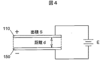
図4は、本発明の第1の実施の形態に係る静電入力装置の並行平板モデルを示す図である。例えば、操作者の手指である検出対象物110とスライド操作検出用タッチ電極150との間の距離をd、対向面積をSとすると、
静電容量Cは、C=ε0εr・S/dで算出できる。
ここで、真空の誘電率:ε0、ベースパネル200の比誘電率:εrである。
FIG. 4 is a diagram showing a parallel plate model of the electrostatic input device according to the first embodiment of the present invention. For example, when the distance between the
The capacitance C can be calculated by C = ε 0 ε r · S / d.
Here, the dielectric constant of vacuum is ε 0 , and the relative dielectric constant of the
図1に示すように、左端部を基準として右方向(Xプラス方向)にXをとると、X=X1の位置で電極間の距離はd1であり、X=X2の位置で電極間の距離はd2である。その間は直線的に形成されている。従って、ベース上面200aを操作者が指でスライド操作すると、指とスライド操作検出用タッチ電極150の距離は、d1からd2の間で変化する。従って、検出される静電容量Cは、上式により接触(近接)位置に応じて変化することになる。
As shown in FIG. 1, when X is taken in the right direction (X plus direction) with the left end as a reference, the distance between the electrodes at the position of X = X1 is d1, and the distance between the electrodes at the position of X = X2. Is d2. In the meantime, it is formed linearly. Therefore, when the operator slides the base
尚、上記示した静電容量Cは、検出信号Vs1、Vs2に基づいて演算により算出することができる。回路定数等の設定あるいは演算時の定数等を調整するキャリブレーションを実施することが好ましい。 The capacitance C shown above can be calculated by calculation based on the detection signals Vs1 and Vs2. It is preferable to perform calibration for setting circuit constants or adjusting constants for calculation.
図5は、本発明の第1の実施の形態に係る静電入力装置の検出容量と横軸時間との関係を示すグラフである。操作者が指を入力センサ部50の左端部の上方向からベース上面200aに向けて近接させ、接触した状態で右方向にスライド操作し、右端部で指を上方向に離間していく場合の検出容量の変化を示すものである。すなわち、操作者が左端部において指を上方向からベース上面200aに向けて接近させ接触させると検出容量は最大値C1まで増加し、その左端部から指を接触させたまま右方向にスライド操作すると検出容量は距離dの変化に従って徐々に低下し、右端部で検出容量がC2になる。操作者が右端部において指を上方向に向ってベース上面200aから離間していくと検出容量がC2からさらに低下していく。
FIG. 5 is a graph showing the relationship between the detection capacity and the horizontal axis time of the electrostatic input device according to the first embodiment of the invention. When the operator moves the finger close to the base
図5において、実線で示すものがスライド操作検出用タッチ電極150によるスライド電極検出容量である。一方、破線で示す矩形状の信号が接触検出用タッチ電極100による接触判定結果であり、Hiレベルが接触状態、Loレベルが非接触状態である。尚、検出対象物のスライド操作検出用タッチ電極150への接触と近接の間に閾値を設定することにより、このHiレベルとLoレベルを適切に設定でき、接触または非接触の状態を判定できる。
In FIG. 5, the solid line indicates the slide electrode detection capacitance by the slide operation
(タッチ操作方向の検出)
図6は、本発明の第1の実施の形態に係る静電入力装置のタッチ操作方向の検出フローチャートである。このフローチャートは、静電入力装置10の入力センサ部50にタッチ入力がされたときの、タッチによるスライド方向を検出するサブルーチンを示している。
(Detection of touch operation direction)
FIG. 6 is a flowchart for detecting the touch operation direction of the electrostatic input device according to the first embodiment of the invention. This flowchart shows a subroutine for detecting a sliding direction by touch when a touch input is made to the input sensor unit 50 of the electrostatic input device 10.
タッチ入力がされると、検出制御部に入力される検出信号Vs1により、まず接触容量検出部482が電極容量を検出する(Step1)。
When touch input is performed, the contact
次に、検出対象物、例えば、操作者の手指が接触検出用タッチ電極100に接触すると検出信号Vs1が変化し、接触判定部484により接触の有無を検出する(Step2)。接触があったと判定された場合はStep3へ進み、接触があったと判定されない場合はメインルーチンへ戻って本フローを終了する。
Next, when a detection object, for example, an operator's finger touches the touch electrode for
スライド操作検出用タッチ電極150により、初期容量を取得しているかいないかを判定する(Step3)。未取得の場合はStep4へ進み、取得済みの場合はStep5へ進む。
It is determined whether or not the initial capacity is acquired by the
スライド操作検出用タッチ電極150から入力される検出信号Vs2に基づきスライド容量検出部481にて初期容量の検出を行なう(Step4)。初期容量を取得した後は、メインルーチンに戻り、スライド操作等による次のタッチ入力待ち状態となる。
Based on the detection signal Vs2 input from the slide operation
既に初期容量が取得されている場合には、スライド操作検出用タッチ電極150から入力される検出信号Vs2に基づきスライド容量検出部481にて現在容量の検出を行なう(Step5)。
If the initial capacity has already been acquired, the current capacity is detected by the slide
次に、初期容量と現在容量の比較をスライド入力位置判定部483にて行なう(Step6)。初期容量と現在容量を比較し、初期容量よりも現在容量の方が大きい場合はStep7へ進み、初期容量よりも現在容量の方が小さい場合はStep8へ進む。
Next, comparison between the initial capacity and the current capacity is performed by the slide input position determination unit 483 (Step 6). The initial capacity is compared with the current capacity. If the current capacity is larger than the initial capacity, the process proceeds to
初期容量よりも現在容量の方が大きい場合は、Xプラス方向検出がされ、これに対応する信号が通信制御部485から車両通信バス500を介して出力され、車両システム600(例えば、オーディオ装置、エアコン装置、カーナビ装置等)が遠隔制御される(Step7)。
When the current capacity is larger than the initial capacity, the X plus direction is detected, and a signal corresponding to this is output from the
初期容量よりも現在容量の方が小さい場合は、Xマイナス方向検出がされ、これに対応する信号が通信制御部485から車両通信バス500を介して出力され、車両システム600(例えば、オーディオ装置、エアコン装置、カーナビ装置等)が遠隔制御される(Step8)。
When the current capacity is smaller than the initial capacity, the X minus direction is detected, and a signal corresponding to this is output from the
Step7またはStep8によりスライド操作方向に対応した出力信号を送出した後は、一旦メインルーチンへ戻って本フローを終了する。
After the output signal corresponding to the slide operation direction is sent in
(本発明の第2の実施の形態に係る静電入力装置)
図7(a)は、本発明の第2の実施の形態に係る静電入力装置の入力センサ部の全体斜視図であり、図7(b)は、入力センサ部を上方向からみた上平面図である。第1の実施の形態と異なるのは、接触検出用タッチ電極100の上部に表面保護パネル240が設けられていることである。また、スライド操作による検出位置の増減を示すような意匠マーク230が表面保護パネル240のパネル上面240aに施されている。図7(b)において、左側のマークの幅W3が徐々に大きくなり右端でのマーク幅W4で最大となるようにされている。その他の構成は、第1の実施の形態と同様であるので、説明を省略する。
(Electrostatic input device according to the second embodiment of the present invention)
FIG. 7A is an overall perspective view of the input sensor unit of the electrostatic input device according to the second embodiment of the present invention, and FIG. 7B is an upper plan view of the input sensor unit viewed from above. FIG. The difference from the first embodiment is that a
図8は、本発明の第2の実施の形態に係る静電入力装置において、左端部を基準として右方向(Xプラス方向)にXをとったときの、位置(距離)及びその位置での電極間距離を示す説明図である。 FIG. 8 shows the position (distance) and the position at the position when X is taken in the right direction (X plus direction) with the left end as a reference in the electrostatic input device according to the second embodiment of the present invention. It is explanatory drawing which shows the distance between electrodes.
図8に示すように、接触検出用タッチ電極100(スライド操作検出用タッチ電極150)の左端部を基準として右方向(Xプラス方向)にXをとると、パネル上面240aからスライド操作検出用タッチ電極150までの距離は、X=0の位置でdA、X=Lの位置でdBである。また、任意の位置、X=LXでの距離はdTである。また、それぞれの位置での静電容量をCA、CB、CXとする。一方、パネル上面240aから接触検出用タッチ電極100までの距離は、XによらずDTであり、そのときの静電容量はCTである。
As shown in FIG. 8, when X is taken in the right direction (X plus direction) with reference to the left end portion of the touch electrode for contact detection 100 (touch electrode for slide operation 150), the touch for detecting slide operation from the panel
第1の実施の形態で説明したのと同様に、静電容量はつぎのようになる。尚、操作者の手指である検出対象物110と接触検出用タッチ電極100及びスライド操作検出用タッチ電極150との間の対向面積Sは一定とする。
CT=ε0εr・S/dT
CX=ε0εr・S/dX
これより、dX=dT・(CT/CX)
As described in the first embodiment, the capacitance is as follows. Note that the facing area S between the
C T = ε 0 ε r · S / d T
C X = ε 0 ε r · S / d X
From this, d X = d T · (C T / C X )
ここで、任意の位置dXは、図8に示したA点とB点との比例計算から次のように求めることができる。
LX=L・(dX―dA)/(dB―dA)
上式に、dX=dT・(CT/CX)を代入すれば、
LX=dT・L/(dB―dA)・(CT/CX)―dA・L/(dB―dA)
上式において、第1項は既知のdT・L/(dB―dA)と測定値により求まる(CT/CX)の積であり、第2項は既知の―dA・L/(dB―dA)である。従って、CT及びCXの測定により、任意のタッチ位置LXが求まる。
Here, the arbitrary position d X, can be determined from the proportional calculation of the points A and B shown in FIG. 8, as follows.
L X = L · (d X -d A ) / (d B -d A )
Substituting d X = d T · (C T / C X ) into the above equation,
L X = d T · L / (d B −d A ) · (C T / C X ) −d A · L / (d B −d A )
In the above equation, the first term is the product of the known d T · L / (d B −d A ) and the measured value (C T / C X ), and the second term is the known −d A · L / (D B -d A ). Accordingly, an arbitrary touch position L X can be obtained by measuring CT and C X.
(タッチ位置の検出)
図9は、本発明の第2の実施の形態に係る静電入力装置のタッチ位置の検出フローチャートである。このフローチャートは、静電入力装置10の入力センサ部50にタッチ入力がされたときの、タッチによる位置を検出するサブルーチンを示している。
(Touch position detection)
FIG. 9 is a flowchart for detecting the touch position of the electrostatic input device according to the second embodiment of the invention. This flowchart shows a subroutine for detecting a touch position when a touch input is made to the input sensor unit 50 of the electrostatic input device 10.
タッチ入力がされると、検出制御部に入力される検出信号Vs1により、まず接触容量検出部482が静電容量を検出する(Step11)。
When touch input is performed, the contact
次に、検出対象物、例えば、操作者の手指がパネル上面240aにタッチして接触検出用タッチ電極100に近接すると検出信号Vs1が変化し、接触判定部484により接触の有無を検出する(Step12)。タッチ(近接)があったと判定された場合はStep13へ進み、タッチ(近接)があったと判定されない場合はメインルーチンへ戻って本フローを終了する。
Next, when a detection object, for example, an operator's finger touches the panel
スライド操作検出用タッチ電極150から入力される検出信号Vs2に基づきスライド容量検出部481にて静電容量CXの検出を行なう(Step13)。
Based on the detection signal Vs2 input from the slide operation
前述のLXを求める式により、測定値に基づいてタッチ操作位置の算出を行なう。Step11で検出した接触検出用タッチ電極100の静電容量CTとStep13で検出したスライド容量検出部481にて静電容量CXの2つの測定値に基づいて算出する。この求められた位置信号LXは通信制御部485から車両通信バス500を介して出力され、車両システム600(例えば、オーディオ装置、エアコン装置、カーナビ装置等)が遠隔制御される(Step14)。この位置信号を送出した後は、一旦メインルーチンへ戻って本フローを終了する。
The formula for the aforementioned L X, to calculate the touch operation position on the basis of the measured values. Based on the two measured values of the capacitance C X at the capacitance C T of the
(本発明の実施の形態の効果)
本発明の実施の形態によれば、次のような効果を有する。
・ 少ない検出電極数、すなわち接触検出用タッチ電極100及びスライド操作検出用タッチ電極150により、検出精度よく、スライド方向および位置の検出を可能とする静電入力装置を提供することができる。これにより、IC化する際に、ポート数が低減できて静電容量検出回路の規模を小さくできるので、コスト低減等も可能となる。
・ 本発明の実施の形態では、接触検出用タッチ電極100により操作者の手指である検出対象物110の接触(タッチ)あるいは近接を判断し、この判断がされた場合にのみタッチ操作方向の検出またはタッチ位置の検出を行なう。これにより、静電容量検出の精度が向上し、確実なタッチ操作方向検出またはタッチ位置検出を行なうことが可能となる。
(3)接触検出用タッチ電極100とスライド操作検出用タッチ電極150は、ベース上面200aの法線方向(Nベクトル)に投影した状態で、図2(b)に示すように、互いに重ならずに所定の間隔W1を有して配置されている。これにより、少なくとも対向面積が干渉しない構成とすることができ、測定される静電容量CTと静電容量CXの検出精度が向上する。
(4)意匠マーク220は、接触検出用タッチ電極100とスライド操作検出用タッチ電極150に略等しい割合で跨ってベース上面200a上に形成されている。これにより、操作者の接触・近接操作は接触検出用タッチ電極100とスライド操作検出用タッチ電極150に均等になされ、静電容量検出の精度が向上する。
(Effect of the embodiment of the present invention)
The embodiment of the present invention has the following effects.
An electrostatic input device that can detect the sliding direction and position with high detection accuracy can be provided by using a small number of detection electrodes, that is, the touch electrode for
In the embodiment of the present invention, contact (touch) or proximity of the
(3) The touch electrode for
(4) The
尚、本発明は上記の実施の形態に限定されるものではなく、その要旨を逸脱しない範囲で種々の態様において実施することが可能である。 In addition, this invention is not limited to said embodiment, It is possible to implement in a various aspect in the range which does not deviate from the summary.
10 …静電入力装置
50 …入力センサ部
100…接触検出用タッチ電極
110…帯電体
150…スライド操作検出用タッチ電極
200…ベースパネル
200a…ベース上面
200b…ベース下面
210…支持パネル
220、230…意匠マーク
240…表面保護パネル
240a…パネル上面
400A、B…発振器
410A、B…アンプ
420A、B…負荷抵抗
430A、B…アンプ
440A、B…BPF
450A、B…整流器
460A、B…LPF
480…検出制御部
481…スライド容量検出部
482…接触容量検出部
483…スライド入力位置判定部
484…接触判定部
485…通信制御部
500…車両通信バス
600…車両システム
DESCRIPTION OF SYMBOLS 10 ... Electrostatic input device 50 ...
450A, B ...
480 ...
Claims (3)
前記第1の電極から離間して設けられ、長尺状に形成された第2の電極と、
前記第1の電極への検出対象物の近接または接触により前記第1の電極から検出される静電容量、及び、前記第2の電極から検出される静電容量に基づいて、前記検出対象物の操作方向または操作位置を検出する検出制御部と、
を有することを特徴とする静電入力装置。 A first electrode formed on the input contact surface or along the input contact surface and formed in an elongated shape;
A second electrode which is provided apart from the first electrode and is formed in an elongated shape;
Based on the capacitance detected from the first electrode by the proximity or contact of the detection target to the first electrode and the capacitance detected from the second electrode, the detection target A detection control unit for detecting the operation direction or operation position of
An electrostatic input device comprising:
The first electrode and the second electrode are arranged at a predetermined interval without overlapping each other in a state projected in the normal direction of the input contact surface. The electrostatic input device according to claim 1 or 2.
Priority Applications (1)
| Application Number | Priority Date | Filing Date | Title |
|---|---|---|---|
| JP2010253695A JP2012104017A (en) | 2010-11-12 | 2010-11-12 | Electrostatic input device |
Applications Claiming Priority (1)
| Application Number | Priority Date | Filing Date | Title |
|---|---|---|---|
| JP2010253695A JP2012104017A (en) | 2010-11-12 | 2010-11-12 | Electrostatic input device |
Publications (1)
| Publication Number | Publication Date |
|---|---|
| JP2012104017A true JP2012104017A (en) | 2012-05-31 |
Family
ID=46394306
Family Applications (1)
| Application Number | Title | Priority Date | Filing Date |
|---|---|---|---|
| JP2010253695A Pending JP2012104017A (en) | 2010-11-12 | 2010-11-12 | Electrostatic input device |
Country Status (1)
| Country | Link |
|---|---|
| JP (1) | JP2012104017A (en) |
Cited By (3)
| Publication number | Priority date | Publication date | Assignee | Title |
|---|---|---|---|---|
| JP2014071734A (en) * | 2012-09-28 | 2014-04-21 | Dainippon Printing Co Ltd | Substrate for color filter integrated touch panel sensor, color filter integrated touch panel sensor, and color filter integrated touch panel module |
| CN110888563A (en) * | 2019-10-29 | 2020-03-17 | 深圳市华星光电半导体显示技术有限公司 | Touch screen and touch display device |
| CN113220205A (en) * | 2020-01-21 | 2021-08-06 | 株式会社东海理化电机制作所 | Remote control device, processing device, and non-transitory computer-readable medium |
Citations (5)
| Publication number | Priority date | Publication date | Assignee | Title |
|---|---|---|---|---|
| JPH09139142A (en) * | 1995-11-16 | 1997-05-27 | Seikosha Co Ltd | Input device |
| JP2004335273A (en) * | 2003-05-08 | 2004-11-25 | Alps Electric Co Ltd | Touch sensor |
| JP2004333302A (en) * | 2003-05-08 | 2004-11-25 | Alps Electric Co Ltd | Touch sensor |
| JP2007242571A (en) * | 2006-03-13 | 2007-09-20 | Fujikura Ltd | Capacitance type switch |
| JP2007329090A (en) * | 2006-06-09 | 2007-12-20 | Nec Corp | Input device |
-
2010
- 2010-11-12 JP JP2010253695A patent/JP2012104017A/en active Pending
Patent Citations (5)
| Publication number | Priority date | Publication date | Assignee | Title |
|---|---|---|---|---|
| JPH09139142A (en) * | 1995-11-16 | 1997-05-27 | Seikosha Co Ltd | Input device |
| JP2004335273A (en) * | 2003-05-08 | 2004-11-25 | Alps Electric Co Ltd | Touch sensor |
| JP2004333302A (en) * | 2003-05-08 | 2004-11-25 | Alps Electric Co Ltd | Touch sensor |
| JP2007242571A (en) * | 2006-03-13 | 2007-09-20 | Fujikura Ltd | Capacitance type switch |
| JP2007329090A (en) * | 2006-06-09 | 2007-12-20 | Nec Corp | Input device |
Cited By (3)
| Publication number | Priority date | Publication date | Assignee | Title |
|---|---|---|---|---|
| JP2014071734A (en) * | 2012-09-28 | 2014-04-21 | Dainippon Printing Co Ltd | Substrate for color filter integrated touch panel sensor, color filter integrated touch panel sensor, and color filter integrated touch panel module |
| CN110888563A (en) * | 2019-10-29 | 2020-03-17 | 深圳市华星光电半导体显示技术有限公司 | Touch screen and touch display device |
| CN113220205A (en) * | 2020-01-21 | 2021-08-06 | 株式会社东海理化电机制作所 | Remote control device, processing device, and non-transitory computer-readable medium |
Similar Documents
| Publication | Publication Date | Title |
|---|---|---|
| US8390272B2 (en) | Position detecting device | |
| TWI525513B (en) | Electrode arrangement for display device | |
| JP4358679B2 (en) | Capacitive proximity sensor | |
| TWI791002B (en) | Non-contact voltage measurement system using multiple capacitors | |
| US20130241578A1 (en) | Capacitance type sensor | |
| JP2007018839A (en) | Capacitive type proximity sensor | |
| US20190050097A1 (en) | Touch panel-equipped display device | |
| JP2013015976A (en) | Multifunction sensor | |
| KR20200095524A (en) | Force sensor mount, and associated housing and system comprising same | |
| KR20140079801A (en) | Electrode device for capacitive sensor device for position detection | |
| US20090166097A1 (en) | Device for improving the accuracy of the touch point on a touch panel and a method thereof | |
| US20200207189A1 (en) | Operation input device and door handle | |
| CN104303136B (en) | Capacitance type sensor, the method for reading capacitance type sensor battle array and the method for manufacturing capacitance type sensor battle array | |
| JP2012104017A (en) | Electrostatic input device | |
| JP2020505617A (en) | Apparatus and method for detecting hard-to-sight configuration with uniform electric field | |
| KR101922014B1 (en) | Capacitive Sensor Device and Method for Calibrating a Capacitive Sensor Device | |
| US9886143B2 (en) | Multi-function sensing apparatus | |
| EP3147765A1 (en) | Operation input device | |
| US9594182B2 (en) | Capacitive positioning device | |
| US7277817B2 (en) | Position sensing device | |
| KR101649750B1 (en) | Proximate Object Detection Method , Proximate Object Detection Apparatus using the same, Touch Detection Method and Touch Detection Apparatus using the Same | |
| US11693143B2 (en) | Scanner for detecting objects behind an opaque surface | |
| US11360606B2 (en) | Control circuit of resistive touch panel | |
| KR20200020082A (en) | Touch sensor module | |
| JP2013257807A (en) | Touch sensor |
Legal Events
| Date | Code | Title | Description |
|---|---|---|---|
| A621 | Written request for application examination |
Free format text: JAPANESE INTERMEDIATE CODE: A621 Effective date: 20130523 |
|
| A977 | Report on retrieval |
Free format text: JAPANESE INTERMEDIATE CODE: A971007 Effective date: 20131128 |
|
| A131 | Notification of reasons for refusal |
Free format text: JAPANESE INTERMEDIATE CODE: A131 Effective date: 20131210 |
|
| A02 | Decision of refusal |
Free format text: JAPANESE INTERMEDIATE CODE: A02 Effective date: 20140430 |