JP2007242571A - Capacitance type switch - Google Patents
Capacitance type switch Download PDFInfo
- Publication number
- JP2007242571A JP2007242571A JP2006067003A JP2006067003A JP2007242571A JP 2007242571 A JP2007242571 A JP 2007242571A JP 2006067003 A JP2006067003 A JP 2006067003A JP 2006067003 A JP2006067003 A JP 2006067003A JP 2007242571 A JP2007242571 A JP 2007242571A
- Authority
- JP
- Japan
- Prior art keywords
- switch
- detection
- capacitance
- detection electrodes
- detection electrode
- Prior art date
- Legal status (The legal status is an assumption and is not a legal conclusion. Google has not performed a legal analysis and makes no representation as to the accuracy of the status listed.)
- Pending
Links
Images

Landscapes
- Switches That Are Operated By Magnetic Or Electric Fields (AREA)
Abstract
Description
本発明は、指などの近接又は接触を検知する静電容量式スイッチに関する。 The present invention relates to a capacitive switch that detects proximity or contact of a finger or the like.
従来より、指などの被検知物体の近接を検知電極によって検出し、この検知電極の静電容量変化から被検知物体の近接を検知することができる非接触又は接触型の静電容量式スイッチが知られている(特許文献1)。 Conventionally, there has been a non-contact or contact-type capacitive switch that can detect the proximity of a detected object such as a finger with a detection electrode and detect the proximity of the detected object from the capacitance change of the detection electrode. Known (Patent Document 1).
このような静電容量式スイッチでは、被検知物体を検出する方法として、直接検知電極のインピーダンスを測定し静電容量を検出することで検知する方法や、検知電極で検出した静電容量を電圧に変換して入力する発信回路を構成し、その発信周波数を測定する方法、RC充放電回路を構成してその放電時間を計測する方法、既知電圧で充電された静電容量を既知容量のコンデンサに移動させて、該既知容量のコンデンサが所定電圧まで充電される時間を測定する方法、または、該既知容量のコンデンサに充放電を繰り返しその回数をカウントする方法などが知られている。
しかしながら、このような静電容量式スイッチでは、操作者が選択するチャンネル数と同数の検知電極を配し、更に、この検知電極毎に静電容量検知回路を設置しなければならないためスイッチ装置の小型化が難しい。 However, in such a capacitance type switch, it is necessary to arrange the same number of detection electrodes as the number of channels selected by the operator and to install a capacitance detection circuit for each detection electrode. Miniaturization is difficult.
また、静電容量検知回路の数を削減するために、複数の検知電極を切り替え装置を介して検知回路に接続し、被検知物体の近接により回路を切り替えるように静電容量式スイッチを構成することが可能である。しかしながら、このような静電容量式スイッチは、切り替え装置を複数配さなければならないため高価であり、また、配線が複雑になるという問題点を有する。 Further, in order to reduce the number of capacitance detection circuits, a plurality of detection electrodes are connected to the detection circuit via a switching device, and the capacitance type switch is configured so that the circuits are switched by the proximity of the detected object. It is possible. However, such a capacitive switch is expensive because a plurality of switching devices must be arranged, and has a problem that wiring is complicated.
本発明はこのような点に鑑みてなされたものであり、簡単な構成でスイッチの小型化を実現することができる静電容量式スイッチを提供することを目的とする。 The present invention has been made in view of such a point, and an object of the present invention is to provide a capacitance type switch that can realize downsizing of the switch with a simple configuration.
本発明の静電容量式スイッチの一態様は、複数のスイッチマークが配列されたスイッチパネルと、前記複数のスイッチマークのうちの一部のスイッチマークの位置に、他のスイッチマークを挟むように分散的に配置された複数の検知電極と、 これら検知電極の静電容量を検知する静電容量検知回路と、この静電容量検知回路の出力に基づいて前記検知電極が配置されたスイッチマーク及び前記検知電極に囲まれたスイッチマークのオン/オフを判断してスイッチオン/オフ信号を出力する制御回路とを備えたことを特徴とする。 In one aspect of the capacitive switch of the present invention, another switch mark is sandwiched between a switch panel in which a plurality of switch marks are arranged and a part of the plurality of switch marks. A plurality of detection electrodes arranged in a distributed manner, a capacitance detection circuit for detecting the capacitance of these detection electrodes, a switch mark on which the detection electrodes are arranged based on the output of the capacitance detection circuit, and And a control circuit for determining on / off of a switch mark surrounded by the detection electrodes and outputting a switch on / off signal.
本発明の静電容量式スイッチによれば、スイッチマークより少ない検知電極を配し、制御回路によって複数の検知電極の静電容量変化を判定することで、隣り合う検知電極間を仮想スイッチとして構成することができる。これにより簡単な構成でスイッチの多チャンネル化を可能とすると共に、静電容量式スイッチの小型化を実現することができる。 According to the capacitance type switch of the present invention, the number of detection electrodes smaller than that of the switch mark is arranged, and a change in capacitance of a plurality of detection electrodes is determined by a control circuit, so that adjacent detection electrodes are configured as virtual switches. can do. Accordingly, it is possible to increase the number of channels of the switch with a simple configuration, and it is possible to reduce the size of the capacitive switch.
以下、添付した図面を参照して本発明の実施の形態について説明する。 Hereinafter, embodiments of the present invention will be described with reference to the accompanying drawings.
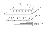
図1は、本発明の第1の実施形態に係る静電容量式スイッチの構成を示す分解斜視図である。 FIG. 1 is an exploded perspective view showing the configuration of the capacitive switch according to the first embodiment of the present invention.
この静電容量式スイッチ100は、被覆材としてのスイッチパネル1と、このスイッチパネル1の裏側に配された複数の検知電極2と、これら検知電極2が接続された制御装置3とを備えて構成されている。
The
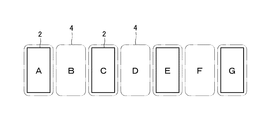
スイッチパネル1は、例えば、樹脂やガラス等の材料により形成され、その上面1aには、スイッチの位置や機能を表示する文字や図形などによるスイッチマーク4が形成されている。このスイッチマーク4は、図2に示すように、検知電極2に対応する位置と、隣り合う検知電極2との間に対応する位置にそれぞれ形成されている。検知電極2は、配線基板5上に所定の間隔を置いて複数配置され、すべて制御装置3に接続されている。制御装置3は、複数の検知電極2が接続されると共に、図示しない外部電気回路に接続されている。なお、配線基板5は、フレキシブルプリント基板、リジットプリント基板や、PET上或いはPEN上の銀回路(又は銅回路)によって構成することができる。
The switch panel 1 is formed of, for example, a material such as resin or glass, and a
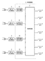
図3は、第1の実施形態に係る静電容量式スイッチ1の電気的構成を示すブロック図である。 FIG. 3 is a block diagram showing an electrical configuration of the capacitive switch 1 according to the first embodiment.
検知電極2は、それぞれ静電容量検知回路10に接続されている。静電容量検知回路10は、検知電極2と接地との間の静電容量Cxに応じた検出値を電圧として出力する。この静電容量検知回路10は、例えば、発振回路を内蔵し、静電容量Cxに応じて発振周波数又はデューティ比が変化する信号を生成するように構成することができる。また、静電容量検知回路10は、制御回路11に接続されている。
Each
次に、このように構成された静電容量式スイッチ100の動作について説明する。
Next, the operation of the
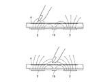
図4は、指が近接したときの同静電容量式スイッチ100の一部断面図である。
FIG. 4 is a partial cross-sectional view of the
ここで、隣り合った検知電極2の一方を検知電極2Aとし、他方を検知電極2Bとし、各検知電極2A,2Bに接続している静電容量検知回路10からの出力を検出値V2A,V2Bとする。図4(a)に示すように、操作者が検知電極2Aと検知電極2Bとの中間に指を近接させると、検知電極2A,2Bから指へほぼ等しい数の電気力線が指に向かう。このとき、検出値V2A及び検出値V2Bはほぼ等しい。また、図4(b)に示すように、操作者が検知電極2Aの近くに指を近接させたときは、検知電極2Aからの電気力線は、検知電極2Bからの電気力線より多くなる。このとき、検出値V2Aは、検出値V2Bより大きい。以下、指の検出位置における検出値2A,2Bとの関係を分類すると次のようになる。
(1)検知電極2Aと検知電極2Bの中間にあるとき:検出値V2A≒検出値V2B
(2)検知電極2A側にあるとき:検出値V2A>検出値V2B
(3)検知電極2B側にあるとき:検出値V2A<検出値V2B
(4)検知電極2A上にあるとき:検出値V2A>>検出値V2B≒0
(5)検知電極2B上にあるとき:0≒検出値V2A<<検出値V2B
制御回路11は、検出値V2A,V2Bを入力してその大小関係を比較することにより以上の5パターンに分類して操作者がどのスイッチSWを選択したのか判定し、それに応じたスイッチ出力を行う。例えば、指が検知電極2A側にあるとき、若しくは指が2A上にあるときは、検知電極2Aが選択されたと判定して検知電極2Aに対応するスイッチ出力を行う。
Here, one of the
(1) When between
(2) When on the
(3) When on the
(4) When on the
(5) When on
The
ここで、制御回路11において、指が検知電極2Aと検知電極2Bの中間にあるときを判断する際には、検出値V2A,V2Bの大小関係がどの程度まで許容するかしきい値を設ける必要がある。以下、そのしきい値の設定方法について説明する。
Here, when the
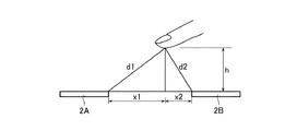
図5は、指と検知電極2との位置を示す概略図である。
FIG. 5 is a schematic diagram showing the positions of the finger and the
指と検知電極2とを平行平板コンデンサと模擬し、d1:指から検知電極2Aまでの距離,d2:指から検知電極2Bまでの距離,h:スイッチパネル1の厚さ,x1:指と検知電極2Aとの水平距離,x2:指と検知電極2Bとの水平距離,C2A:検知電極2Aから検知される静電容量,C2B:検知電極2Bから検知される静電容量と定義すると、以下のような関係式が成り立つ。なお、ここでは指がスイッチパネル1に接触した状態とする。
式(1)d1=εS/C2A
式(2)d2=εS/C2B
更に、式(1),式(2)及び図5より、以下の関係式が成り立つ。
式(3)x12=(εS/C2A)2−h2
式(4)x22=(εS/C2B)2−h2
ここで、隣り合うスイッチの境界位置を、予めx1とx2によって定められる任意の位置に決定すれば、式(3)及び式(4)によってその境界位置における静電容量C2A,C2Bが定まる。この静電容量C2A,C2Bに基づいて、しきい値を決めればよい。なお、ここでは指と検知電極を平行平板として仮定したが、実際には、センサの形状や寸法に従ってしきい値を決めればよい。
Simulating finger and
Formula (1) d1 = εS / C 2A
Formula (2) d2 = εS / C 2B
Furthermore, the following relational expressions hold from Expression (1), Expression (2), and FIG.
Formula (3) x1 2 = (εS / C 2A ) 2 -h 2
Formula (4) x2 2 = (εS / C 2B ) 2 -h 2
Here, if the boundary position of the adjacent switches is determined to be an arbitrary position determined in advance by x1 and x2, the capacitances C 2A and C 2B at the boundary position are determined by Expression (3) and Expression (4). . The threshold value may be determined based on the capacitances C 2A and C 2B . Although the finger and the detection electrode are assumed to be parallel plates here, the threshold value may actually be determined according to the shape and dimensions of the sensor.
このように、指が近接した近くの検知電極2A,2Bからの検出値V2A,V2Bを制御回路11によって判定することで、隣り合う検知電極2間を仮想スイッチとして構成することができる。本発明によれば、検知電極がN(Nは2以上の自然数)個配されていれば、スイッチのチャンネルを(2N−1)個とすることができる。これによりスイッチの多チャンネル化を可能とすると共に、静電容量式スイッチの小型化を実現することができる。
As described above, the detection values V 2A and V 2B from the
なお、本実施形態では、各検知電極2にそれぞれ静電容量検知回路10を接続したが、切り替器などを使用して、複数の検知電極2で1つの静電容量検知回路10を共用するようにしてもよい。
In this embodiment, the
図6は、本発明の第2の実施形態に係る静電容量式スイッチの構成を示す要部拡大図である。 FIG. 6 is an enlarged view of a main part showing the configuration of the capacitive switch according to the second embodiment of the present invention.
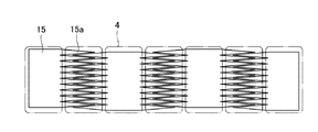
第1の実施形態では、図2に示すように、複数の矩形状の検知電極2が所定の距離を置いて配されているが、第2の実施形態では、図6に示すように、検知電極15のうち他の検知電極15と隣り合う辺を櫛歯状に形成し(15a)、隙間を介して互いの櫛歯部15aが歯合するよう検知電極15同士を重み付けされている。ここでは、互いの櫛歯部15aが重なり合った部分が仮想スイッチとして機能する。また、本実施形態の電気的構成は、第1の実施形態と同様であり、各検知電極15で検出された静電容量は、検出値に変換されて制御回路11に出力される。
In the first embodiment, a plurality of
以下に、このように構成された第2の実施形態に係る静電容量式スイッチにおける制御回路11の判定方法について説明する。
Hereinafter, a determination method of the
隣り合う検知電極15の一方を検知電極15Aとし、他方を検知電極15Bとし、それぞれから検知される静電容量をC15A,C15Bとすると、以下の関係式が成り立つ。なお、S15A:指が覆う検知電極15Aの面積,S15B:指が覆う検知電極15Bの面積,ε:スイッチパネル1の誘電率である。ここで、検知電極15A及び検知電極15Bは互いに近接して配されているため、指と検知電極15A及び15Bとの距離は等しいと仮定でき、指と検知電極15A及び15Bとの距離をスイッチパネル1の厚さhとする。
式(5)C15A/C15B=(ε・S15A/h)/(ε・S15B/h)=S15A/S15B
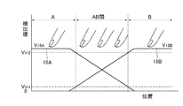
式(5)に示すように、検知電極15A及び検知電極15Bから検出される静電容量C15Aと静電容量C15Bとの比は、指が覆う検知電極15Aの面積S15Aと指が覆う検知電極15B及びの面積S15Bの比として扱うことができる。この指の位置と、検知電極15から検出される静電容量の関係を図7に示す。この静電容量C15A,C15Bは、それぞれ検出値V15A,V15Bに変換され制御回路11に出力される。制御回路11は、検出値V15A,V15Bと2つのしきい値Vth1、Vth2とを比較し、以下(1)〜(3)に示すような判定を行う。
(1)V15A>Vth2かつV15B<Vth1ならばAの領域のスイッチがON
(2)V15A<Vth1かつV15B>Vth2ならばBの領域のスイッチがON
(3)Vth1<V15A<Vth2かつVth1<V15B<Vth2ならばAB間の領域のスイッチがON
このように隣り合う検知電極15を重み付けするように構成することで、検知電極15間における指の近接の検知感度を向上させることができる。
Assuming that one of the
Expression (5) C 15A / C 15B = (ε · S 15A / h) / (ε · S 15B / h) = S 15A / S 15B
As shown in Equation (5), the ratio of the capacitance C 15A and the capacitance C 15B detected from the
(1) If V 15A > V th2 and V 15B <V th1 , the switch in area A is ON
(2) If V 15A <V th1 and V 15B > V th2 , the switch in area B is ON
(3) If V th1 <V 15A <V th2 and V th1 <V 15B <V th2 , the switch in the area between AB is ON
Thus, the detection sensitivity of the proximity | contact of the finger | toe between the
また、検知電極2の重み付けは図7のような形状に限らず、指の近接する位置により隣り合う検知電極で検出される静電容量が変化すればよい。
Further, the weighting of the
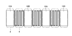
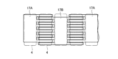
図8〜図11は、他の重み付けした検知電極の構成例を示す図である。 8 to 11 are diagrams showing examples of the configuration of other weighted detection electrodes.
検知電極16A(17A)の隣り合う他の検知電極16B(17B)と接する辺において、電極配列方向(図8)又はそれと直交する方向(図9)に配列された矩形の櫛歯部を形成し、所定の隙間を介して櫛歯部が歯合するように検知電極を配することができる。なお、図8に示す櫛歯部は、検知電極16A、16Bから遠ざかる程、その幅が狭くなるようにして隣接する検知電極16A、16Bの面積比を位置によって変えるようにしている。
On the side of the
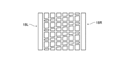
更に、図10に示すように、多層リジットプリント基板や、多層フレキシブルプリント基板上において、第1の実施形態に係る検知電極を細かい検知電極18L、18Rに分離し、検知電極18L及び18Rとを異なる層に配置して各層の検知電極18L、18Rを相互接続するように構成することができる。このように検知電極を任意の形状に構成することができる。
Furthermore, as shown in FIG. 10, the detection electrodes according to the first embodiment are separated into
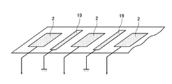
図11は、本発明の第3の実施形態に係る静電容量式スイッチの構成を示す要部拡大図である。 FIG. 11 is an enlarged view of a main part showing the configuration of the capacitive switch according to the third embodiment of the present invention.
この実施形態では、隣り合う検知電極2の間に接地電極19が形成されている。このように検知電極2間に接地電極19を備えることによって、検知電極2が近接して配されていても、図12に示すように、隣接した検知電極2からの電気力線は接地電極19に結合して他の検知電極2に作用しないので誤作動を防止することができる。
In this embodiment, a
上述した実施形態では、検知電極間に1つの仮想スイッチを配しているが、制御回路において検知電極から検出される検出値を複数のしきい値によって判定することで、2つの検知電極の間に複数の仮想スイッチを構成することができる。 In the above-described embodiment, one virtual switch is arranged between the detection electrodes. However, the detection value detected from the detection electrode in the control circuit is determined by a plurality of threshold values, so that the two detection electrodes are arranged. A plurality of virtual switches can be configured.
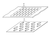
また、上述した実施形態では、スイッチマーク及び検知電極を直線上に配置しているが、例えば図13に示すように、スイッチマーク4’及び検知電極2’を平面的にマトリクス状に配するなど任意の位置に配置することができる。
In the above-described embodiment, the switch marks and the detection electrodes are arranged on a straight line. However, as shown in FIG. 13, for example, the switch marks 4 ′ and the
また、上述した実施形態では、隣り合う2つの検知電極で検知される静電容量を比較したが、例えば、スイッチが2次元的に配置される場合のように、上下左右等に3つ以上の検知電極4’を配置し、各検知電極4’から検知される静電容量を静電容量検知回路2’で検出し比較するように構成することもできる。
In the above-described embodiment, the capacitance detected by the two adjacent detection electrodes is compared. For example, as in the case where the switches are two-dimensionally arranged, three or more are provided in the upper, lower, left, and right sides. It is also possible to arrange the
1…スイッチパネル、2,15〜17…検知電極、3…制御装置、4…スイッチマーク、5…配線基板、10…静電容量検知回路、11…制御回路、18…接地電極、100…静電容量式スイッチ。 DESCRIPTION OF SYMBOLS 1 ... Switch panel, 2, 15-17 ... Detection electrode, 3 ... Control apparatus, 4 ... Switch mark, 5 ... Wiring board, 10 ... Electrostatic capacity detection circuit, 11 ... Control circuit, 18 ... Ground electrode, 100 ... Static Capacitive switch.
Claims (4)
前記複数のスイッチマークのうちの一部のスイッチマークの位置に、他のスイッチマークを挟むように分散的に配置された複数の検知電極と、
これら検知電極の静電容量を検知する静電容量検知回路と、
この静電容量検知回路の出力に基づいて前記検知電極が配置されたスイッチマーク及び前記検知電極に囲まれたスイッチマークのオン/オフを判断してスイッチオン/オフ信号を出力する制御回路と
を備えたことを特徴とする静電容量式スイッチ。 A switch panel in which a plurality of switch marks are arranged;
A plurality of detection electrodes arranged in a distributed manner so as to sandwich another switch mark at the position of a part of the plurality of switch marks,
A capacitance detection circuit for detecting the capacitance of these detection electrodes;
A control circuit for determining on / off of a switch mark on which the detection electrode is arranged and a switch mark surrounded by the detection electrode based on an output of the capacitance detection circuit and outputting a switch on / off signal; Capacitance type switch characterized by comprising.
前記検知電極は、前記複数のスイッチマークの一番端から奇数番目のスイッチマークの位置のみに配置されている
ことを特徴とする請求項1記載の静電容量式スイッチ。 The switch marks are arranged in an odd number one-dimensionally,
The capacitance type switch according to claim 1, wherein the detection electrode is arranged only at a position of an odd-numbered switch mark from an end of the plurality of switch marks.
ことを特徴とする請求項1又は2記載の静電容量式スイッチ。 The capacitance type according to claim 1 or 2, wherein the adjacent detection electrodes are arranged so that portions adjacent to each other are formed in a comb-like shape and are engaged with each other through a predetermined gap. switch.
Priority Applications (1)
| Application Number | Priority Date | Filing Date | Title |
|---|---|---|---|
| JP2006067003A JP2007242571A (en) | 2006-03-13 | 2006-03-13 | Capacitance type switch |
Applications Claiming Priority (1)
| Application Number | Priority Date | Filing Date | Title |
|---|---|---|---|
| JP2006067003A JP2007242571A (en) | 2006-03-13 | 2006-03-13 | Capacitance type switch |
Publications (1)
| Publication Number | Publication Date |
|---|---|
| JP2007242571A true JP2007242571A (en) | 2007-09-20 |
Family
ID=38587889
Family Applications (1)
| Application Number | Title | Priority Date | Filing Date |
|---|---|---|---|
| JP2006067003A Pending JP2007242571A (en) | 2006-03-13 | 2006-03-13 | Capacitance type switch |
Country Status (1)
| Country | Link |
|---|---|
| JP (1) | JP2007242571A (en) |
Cited By (15)
| Publication number | Priority date | Publication date | Assignee | Title |
|---|---|---|---|---|
| JP2009272043A (en) * | 2008-04-30 | 2009-11-19 | Pentel Corp | Capacitance type switch device |
| JP2010108314A (en) * | 2008-10-30 | 2010-05-13 | Pentel Corp | Input device |
| KR100983886B1 (en) * | 2008-04-28 | 2010-09-28 | 주식회사 카모스 | capacitor switch |
| JP2010250675A (en) * | 2009-04-17 | 2010-11-04 | Mitsubishi Electric Corp | Operation interface |
| WO2010135072A3 (en) * | 2009-05-22 | 2011-02-03 | Freescale Semiconductor Inc. | Device with proximity detection capability |
| JP2012104017A (en) * | 2010-11-12 | 2012-05-31 | Tokai Rika Co Ltd | Electrostatic input device |
| WO2014162668A1 (en) * | 2013-04-01 | 2014-10-09 | 株式会社デンソー | Capacitance-type switch |
| JP2014203542A (en) * | 2013-04-01 | 2014-10-27 | 株式会社デンソー | Electrostatic capacity type switch |
| JP2014203541A (en) * | 2013-04-01 | 2014-10-27 | 株式会社デンソー | Electrostatic capacity type switch |
| JP2014203540A (en) * | 2013-04-01 | 2014-10-27 | 株式会社デンソー | Electrostatic capacity type switch |
| JP2014212100A (en) * | 2013-04-01 | 2014-11-13 | 株式会社デンソー | Capacitance-type switch |
| CN105074863A (en) * | 2013-04-01 | 2015-11-18 | 株式会社电装 | Electrostatic capacitance-type switch |
| JP2017531269A (en) * | 2014-07-16 | 2017-10-19 | ベガ グリースハーバー カーゲーVega Grieshaber Kg | Magnetic field device having an input unit |
| JP2018054261A (en) * | 2016-09-30 | 2018-04-05 | シャープ株式会社 | Electrical apparatus |
| JP2021114365A (en) * | 2020-01-16 | 2021-08-05 | 株式会社東海理化電機製作所 | Operation device |
-
2006
- 2006-03-13 JP JP2006067003A patent/JP2007242571A/en active Pending
Cited By (18)
| Publication number | Priority date | Publication date | Assignee | Title |
|---|---|---|---|---|
| KR100983886B1 (en) * | 2008-04-28 | 2010-09-28 | 주식회사 카모스 | capacitor switch |
| JP2009272043A (en) * | 2008-04-30 | 2009-11-19 | Pentel Corp | Capacitance type switch device |
| JP2010108314A (en) * | 2008-10-30 | 2010-05-13 | Pentel Corp | Input device |
| JP2010250675A (en) * | 2009-04-17 | 2010-11-04 | Mitsubishi Electric Corp | Operation interface |
| WO2010135072A3 (en) * | 2009-05-22 | 2011-02-03 | Freescale Semiconductor Inc. | Device with proximity detection capability |
| US8115499B2 (en) | 2009-05-22 | 2012-02-14 | Freescale Semiconductor, Inc. | Device with proximity detection capability |
| JP2012104017A (en) * | 2010-11-12 | 2012-05-31 | Tokai Rika Co Ltd | Electrostatic input device |
| JP2014203542A (en) * | 2013-04-01 | 2014-10-27 | 株式会社デンソー | Electrostatic capacity type switch |
| WO2014162668A1 (en) * | 2013-04-01 | 2014-10-09 | 株式会社デンソー | Capacitance-type switch |
| JP2014203541A (en) * | 2013-04-01 | 2014-10-27 | 株式会社デンソー | Electrostatic capacity type switch |
| JP2014203540A (en) * | 2013-04-01 | 2014-10-27 | 株式会社デンソー | Electrostatic capacity type switch |
| JP2014212100A (en) * | 2013-04-01 | 2014-11-13 | 株式会社デンソー | Capacitance-type switch |
| CN105074863A (en) * | 2013-04-01 | 2015-11-18 | 株式会社电装 | Electrostatic capacitance-type switch |
| US9608629B2 (en) | 2013-04-01 | 2017-03-28 | Denso Corporation | Use of relative permittivity in different materials to enhance capacitive switch sensitivity |
| JP2017531269A (en) * | 2014-07-16 | 2017-10-19 | ベガ グリースハーバー カーゲーVega Grieshaber Kg | Magnetic field device having an input unit |
| JP2018054261A (en) * | 2016-09-30 | 2018-04-05 | シャープ株式会社 | Electrical apparatus |
| JP2021114365A (en) * | 2020-01-16 | 2021-08-05 | 株式会社東海理化電機製作所 | Operation device |
| JP7372844B2 (en) | 2020-01-16 | 2023-11-01 | 株式会社東海理化電機製作所 | operating device |
Similar Documents
| Publication | Publication Date | Title |
|---|---|---|
| JP2007242571A (en) | Capacitance type switch | |
| JP2007240479A (en) | Capacitance type position detector | |
| JP6032371B2 (en) | Detection sensor and input device | |
| EP2333648B1 (en) | Position detecting device | |
| EP3183638B1 (en) | Electrode arrangement for and method of gesture detection and tracking | |
| US8456427B2 (en) | Floating capacitive couplers used to enhance signal coupling in a capacitive touchpad | |
| US10120478B2 (en) | Piezo based force sensing | |
| JP4333428B2 (en) | Proximity position input device | |
| JP6714959B2 (en) | Input device | |
| JP4833729B2 (en) | Capacitive sensor | |
| EP2466433A2 (en) | Capacitive touch panel | |
| JP2005353565A (en) | Hybrid sensor and electrostatic capacity type proximity sensor | |
| JP2009037373A (en) | Touch panel input device | |
| JP2005337773A (en) | Electrostatic capacitance type detecting device | |
| KR20120002446A (en) | Capacitance sensor and information input apparatus | |
| JP2008004465A (en) | Electrostatic capacity type switch | |
| KR20180017000A (en) | Sensor structure for improved touch and gesture decoding | |
| JP4286207B2 (en) | Capacitance type coordinate detection device | |
| KR101553604B1 (en) | Touch detecting apparatus and method | |
| JP6124301B2 (en) | Capacitive input device | |
| JPH09212302A (en) | Coordinate input device | |
| JP6001764B2 (en) | Touch detection module and contact touch detection method in the touch detection module | |
| JP6096421B2 (en) | Touch switch input device | |
| KR20110128533A (en) | Capacitive input device having duplex structure | |
| JP5605577B2 (en) | Capacitive touch sensor |