JP2012054616A - Plasma etching method - Google Patents
Plasma etching method Download PDFInfo
- Publication number
- JP2012054616A JP2012054616A JP2011273076A JP2011273076A JP2012054616A JP 2012054616 A JP2012054616 A JP 2012054616A JP 2011273076 A JP2011273076 A JP 2011273076A JP 2011273076 A JP2011273076 A JP 2011273076A JP 2012054616 A JP2012054616 A JP 2012054616A
- Authority
- JP
- Japan
- Prior art keywords
- etching
- semiconductor substrate
- plasma
- temperature
- gas
- Prior art date
- Legal status (The legal status is an assumption and is not a legal conclusion. Google has not performed a legal analysis and makes no representation as to the accuracy of the status listed.)
- Pending
Links
Images


Abstract
Description
本発明は、ワイドギャップ半導体基板をプラズマエッチングするプラズマエッチング方法に関する。 The present invention relates to a plasma etching method for plasma etching a wide gap semiconductor substrate.
半導体の分野では、従来から、シリコン基板(Si基板)が基板材料として広く用いられているが、近年、このシリコン基板よりも物性の優れたワイドギャップ半導体基板が着目されている。このワイドギャップ半導体基板は、一般にシリコンやガリウムヒ素(GaAs)に比べて結晶の格子定数が小さくバンドギャップが大きいという特徴を持っており、例えば、炭化珪素(SiC),窒化ガリウム(GaN),窒化アルミニウム(AlN),酸化亜鉛(ZnO),窒化ホウ素(BN)及びリン化ホウ素(BP)等、ホウ素(B),炭素(C),窒素(N)及び酸素(O)のうちの少なくとも1種を含んで構成されるものである。 Conventionally, in the field of semiconductors, silicon substrates (Si substrates) have been widely used as substrate materials, but in recent years, wide gap semiconductor substrates having better physical properties than silicon substrates have attracted attention. This wide gap semiconductor substrate is generally characterized by a smaller crystal lattice constant and a larger band gap than silicon and gallium arsenide (GaAs). For example, silicon carbide (SiC), gallium nitride (GaN), nitride At least one of boron (B), carbon (C), nitrogen (N) and oxygen (O), such as aluminum (AlN), zinc oxide (ZnO), boron nitride (BN) and boron phosphide (BP) It is comprised including.
そして、このワイドギャップ半導体基板は、結晶の格子定数が小さい、つまり、原子間の結合が強く、優れた物性を有する反面、原子間の結合が強いためにエッチング加工を行い難いという欠点を有している。そこで、従来、このような半導体基板をプラズマエッチングする方法として、例えば、特開2008−294210号公報に開示された、炭化珪素基板に関するプラズマエッチング方法が提案されている。 And this wide gap semiconductor substrate has a defect that the lattice constant of the crystal is small, that is, the bond between atoms is strong and has excellent physical properties, but the etching process is difficult because of the strong bond between atoms. ing. Therefore, conventionally, as a method for plasma etching such a semiconductor substrate, for example, a plasma etching method for a silicon carbide substrate disclosed in Japanese Patent Application Laid-Open No. 2008-294210 has been proposed.
このプラズマエッチング方法は、所定形状のマスクパターンを備えた二酸化珪素膜(SiO2膜)を炭化珪素基板の表面に形成するマスク形成工程と、SF6ガス,O2ガス及びArガスの混合ガスをエッチングガスとして用い、前記二酸化珪素膜をマスクとして、前記炭化珪素基板をプラズマエッチングする第1エッチング工程と、Arガス及びO2ガスの混合ガスをエッチングガスとして用い、前記二酸化珪素膜をマスクとして、前記炭化珪素基板をプラズマエッチングする第2エッチング工程とを順次実施するというものであり、前記第1エッチング工程では、SF6ガス,O2ガス及びArガスの割合を所定の割合とし、雰囲気圧力を0.5Pa以下とし、炭化珪素基板を70℃〜100℃に加熱し、前記第2エッチング工程では、Arガス及びO2ガスの割合を所定の割合とし、雰囲気圧力を0.5Pa以下とし、炭化珪素基板を70℃〜100℃に加熱するようになっている。 In this plasma etching method, a mask forming step of forming a silicon dioxide film (SiO 2 film) having a mask pattern of a predetermined shape on the surface of a silicon carbide substrate, and a mixed gas of SF 6 gas, O 2 gas and Ar gas are used. A first etching step of plasma etching the silicon carbide substrate using the silicon dioxide film as a mask using the etching gas, a mixed gas of Ar gas and O 2 gas as an etching gas, and using the silicon dioxide film as a mask The second etching step of plasma etching the silicon carbide substrate is sequentially performed. In the first etching step, the ratio of SF 6 gas, O 2 gas and Ar gas is set to a predetermined ratio, and the atmospheric pressure is set to a predetermined value. 0.5 Pa or less, the silicon carbide substrate is heated to 70 ° C. to 100 ° C., and in the second etching step, , And the ratio a predetermined ratio of Ar gas and O 2 gas, the atmosphere pressure of less 0.5 Pa, so as to heat the silicon carbide substrate 70 ° C. to 100 ° C..
ところで、例えば、シリコン(Si)をプラズマエッチングする場合、基板の温度は、通常、100℃までの温度に制限される。これは、基板の温度が100℃を超えると、エッチングが等方的に進み易くなることや保護膜が形成され難くなることによってエッチング形状が悪化する(異方性エッチングを行い難くなる)、マスクとなるレジスト膜の耐熱性が低いため、レジスト膜の軟化によってマスクパターンの形状精度が低下する、といった問題を生じるからである。また、二酸化珪素(SiO2)をプラズマエッチングする場合においても、マスクとなるレジスト膜の耐熱性が低いという問題から、上記と同様、当該基板の加熱温度は100℃までの温度に制限されるのが一般的である。 By the way, for example, when plasma etching of silicon (Si), the temperature of the substrate is usually limited to a temperature of up to 100 ° C. This is because when the temperature of the substrate exceeds 100 ° C., the etching is likely to proceed isotropically or the protective film is difficult to be formed, so that the etching shape is deteriorated (it is difficult to perform anisotropic etching). This is because the resist film having low heat resistance causes a problem that the shape accuracy of the mask pattern decreases due to the softening of the resist film. Also, when plasma etching silicon dioxide (SiO 2 ), the heating temperature of the substrate is limited to a temperature of up to 100 ° C., as described above, due to the low heat resistance of the resist film serving as a mask. Is common.
そして、上記従来のプラズマエッチング方法においても、炭化珪素基板は70℃〜100℃に加熱されてエッチングされており、前記シリコンや二酸化珪素と同様に、100℃までの温度に制御されている。 In the conventional plasma etching method as well, the silicon carbide substrate is etched by being heated to 70 ° C. to 100 ° C., and the temperature is controlled to 100 ° C. similarly to the silicon and silicon dioxide.
しかしながら、本願発明者らは、鋭意研究を重ねた結果、プラズマエッチングの対象となる基板が、原子間の結合が強いワイドギャップ半導体基板であるときには、当該半導体基板を100℃よりも更に高い温度に加熱してエッチングすると、エッチング加工精度が向上することを知見するに至った。 However, as a result of intensive studies, the inventors of the present application have made the semiconductor substrate a temperature higher than 100 ° C. when the substrate to be subjected to plasma etching is a wide gap semiconductor substrate having strong bonds between atoms. It came to know that etching accuracy improves when heated and etched.
本発明は、本願発明者らが、精度の良いプラズマエッチングを実施可能なワイドギャップ半導体基板の加熱温度について実験を重ねた結果なされたものであり、ワイドギャップ半導体基板を高精度にエッチングすることができるプラズマエッチング方法の提供をその目的とする。 The present invention has been made as a result of repeated experiments conducted by the inventors of the present invention on the heating temperature of a wide gap semiconductor substrate capable of performing high-precision plasma etching, and the wide gap semiconductor substrate can be etched with high accuracy. An object of the present invention is to provide a plasma etching method.
上記目的を達成するための本発明は、
閉塞空間を有する処理チャンバと、ワイドギャップ半導体基板が載置される基台と、前記処理チャンバ内を減圧する排気装置と、前記処理チャンバ内にガスを供給するガス供給装置と、環状のコイルとを有し、このコイルに高周波電力を供給して、前記処理チャンバ内に供給されたガスをプラズマ化するプラズマ生成装置と、前記基台に高周波電力を供給する高周波電源とを備えたエッチング装置を用いて、前記基台上のワイドギャップ半導体基板をプラズマエッチングする方法であって、
前記基台上に前記ワイドギャップ半導体基板を載置した後、前記排気装置によって減圧された前記処理チャンバ内に、前記ガス供給装置によってエッチングガスを供給し、供給したエッチングガスを前記プラズマ生成装置によってプラズマ化し、且つ、前記高周波電源によって前記基台にバイアス電位を与えて前記ワイドギャップ半導体基板をエッチングするとともに、前記ワイドギャップ半導体基板を200℃〜400℃に加熱した状態でエッチングするようにしたことを特徴とするプラズマエッチング方法に係る。
To achieve the above object, the present invention provides:
A processing chamber having a closed space; a base on which a wide gap semiconductor substrate is placed; an exhaust device that depressurizes the processing chamber; a gas supply device that supplies gas into the processing chamber; and an annular coil; An etching apparatus comprising: a plasma generating device that supplies high-frequency power to the coil to convert the gas supplied into the processing chamber into plasma; and a high-frequency power source that supplies high-frequency power to the base. A method of plasma etching a wide gap semiconductor substrate on the base, comprising:
After placing the wide gap semiconductor substrate on the base, an etching gas is supplied by the gas supply device into the processing chamber decompressed by the exhaust device, and the supplied etching gas is supplied by the plasma generation device. The plasma is generated, and the wide gap semiconductor substrate is etched by applying a bias potential to the base by the high frequency power source, and the wide gap semiconductor substrate is etched while being heated to 200 ° C. to 400 ° C. The present invention relates to a plasma etching method.
この発明によれば、ワイドギャップ半導体基板(以下、単に「半導体基板」と言う。)をプラズマエッチングするに当たり、当該半導体基板を200℃〜400℃に加熱している。このようにしているのは、本願発明者らの研究の結果、前記エッチング装置を用いて、原子間の結合が強い半導体基板をエッチングする際には、当該半導体基板の加熱温度は200℃〜400℃であることが好ましいと判明したからである。 According to the present invention, when plasma etching a wide gap semiconductor substrate (hereinafter simply referred to as “semiconductor substrate”), the semiconductor substrate is heated to 200 ° C. to 400 ° C. This is because, as a result of the study by the inventors of the present application, when a semiconductor substrate having a strong bond between atoms is etched using the etching apparatus, the heating temperature of the semiconductor substrate is 200 ° C. to 400 ° C. It is because it became clear that it was preferable that it was (degreeC).
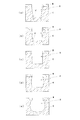
即ち、本願発明者らの研究によると、半導体基板Kの加熱温度が低いときには、図2(a)に示すように、エッチングにより形成された穴Hや溝Hの底面の側壁側に溝H’が更に形成され、精度の良いエッチング形状を得ることができない。ところが、半導体基板Kの加熱温度を徐々に高くしていくと、図2(b)に示すように、形成される溝H’の大きさが徐々に小さくなり、最終的には、図2(c)に示すように、溝H’が形成されなくなる。 That is, according to the study by the present inventors, when the heating temperature of the semiconductor substrate K is low, as shown in FIG. 2A, the hole H formed by etching or the groove H ′ on the side wall side of the bottom surface of the groove H is formed. Is further formed, and an accurate etching shape cannot be obtained. However, when the heating temperature of the semiconductor substrate K is gradually increased, as shown in FIG. 2B, the size of the groove H ′ to be formed gradually decreases, and finally, FIG. As shown in c), the groove H ′ is not formed.
また、溝H’が形成されなくなった加熱温度から半導体基板Kの加熱温度を徐々に高くしていくと、エッチングが等方的に進み易くなり、図2(d)及び図2(e)に示すように、穴Hや溝Hの側壁までエッチングされてしまう。半導体基板Kを構成する原子は、その結合が切れてからでないと、エッチングガスのプラズマ化により生成されたラジカルやイオンと反応しないのであるが、当該半導体基板Kの温度が高いほど、原子間の結合が切れ易く、エッチングガスのプラズマ化により生成されたラジカルやイオンと、半導体基板Kを構成する原子とが反応し易いため、この反応によるエッチングが効率的に進む。尚、半導体基板Kを構成し得る上述した材料の内、特に炭化珪素については、シリコン(Si)と炭素(C)との結合が強固である一方、その温度が高くなることによって両者の結合が切れ易く、エッチングされ易い。したがって、半導体基板Kの加熱温度が高いほど、ワイドギャップ半導体基板Kのエッチングが等方的に進み、穴Hや溝Hの側壁がエッチングされ易くなる。尚、図2(d)と図2(e)では、図2(e)の方が半導体基板Kの加熱温度が高いときのエッチング形状を図示している。また、図2において、符号Mはマスクを示している。 Further, when the heating temperature of the semiconductor substrate K is gradually increased from the heating temperature at which the groove H ′ is no longer formed, the etching is likely to proceed isotropically, as shown in FIGS. 2 (d) and 2 (e). As shown, the sidewalls of the hole H and the groove H are etched. The atoms constituting the semiconductor substrate K do not react with the radicals and ions generated by the plasma formation of the etching gas unless the bond is broken. However, the higher the temperature of the semiconductor substrate K, the more Since the bonds are easily broken and radicals and ions generated by making the etching gas into plasma easily react with atoms constituting the semiconductor substrate K, etching by this reaction proceeds efficiently. Of the above-described materials that can constitute the semiconductor substrate K, particularly silicon carbide, the bond between silicon (Si) and carbon (C) is strong, but the bond between the two increases as the temperature increases. Easy to cut and easy to etch. Therefore, as the heating temperature of the semiconductor substrate K increases, the etching of the wide gap semiconductor substrate K progresses isotropically, and the sidewalls of the holes H and the grooves H are easily etched. 2D and 2E show the etching shape when the heating temperature of the semiconductor substrate K is higher in FIG. 2E. Moreover, in FIG. 2, the code | symbol M has shown the mask.
そして、このような点を踏まえ、半導体基板の加熱温度とエッチング形状との関係について調べたところ、半導体基板の加熱温度が200℃〜400℃であれば、プラズマエッチングを行った際に、穴Hや溝Hの底面に溝H’が全く形成されないか、形成されたとしても非常に小さなものであり、また、穴Hや溝Hの側壁についても、全くエッチングされないか、エッチングされたとしてもごく僅かであることが確認された。したがって、半導体基板を200℃〜400℃に加熱すれば、半導体基板を高精度にエッチングすることができる。尚、半導体基板の加熱温度は300℃〜400℃の範囲であれば、更に好ましい。 Based on these points, the relationship between the heating temperature of the semiconductor substrate and the etching shape was examined. If the heating temperature of the semiconductor substrate was 200 ° C. to 400 ° C., the hole H was removed when plasma etching was performed. The groove H ′ is not formed at all on the bottom surface of the groove H or the groove H ′ is very small even if it is formed, and the side wall of the hole H or the groove H is not etched at all or is etched very little. It was confirmed that it was slight. Therefore, if the semiconductor substrate is heated to 200 ° C. to 400 ° C., the semiconductor substrate can be etched with high accuracy. The heating temperature of the semiconductor substrate is more preferably in the range of 300 ° C to 400 ° C.
斯くして、本発明に係るプラズマエッチング方法によれば、半導体基板をプラズマエッチングする際に、この半導体基板を200℃〜400℃に加熱しているので、精度良く半導体基板をエッチングすることができる。 Thus, according to the plasma etching method of the present invention, when the semiconductor substrate is plasma-etched, since the semiconductor substrate is heated to 200 ° C. to 400 ° C., the semiconductor substrate can be etched with high accuracy. .
ところで、半導体基板の温度を、加熱前の温度T0からエッチング処理時の温度T1(200℃≦T1≦400℃)まで温度上昇させるには、図3に示すように、一定の時間がかかる。そして、半導体基板の温度がエッチング処理温度T1に達する前からエッチングガスを処理チャンバ内に供給して半導体基板のエッチングを開始すると、エッチングの開始から半導体基板の温度がエッチング処理温度T1に達するまでの間は、当該半導体基板の温度変化によってエッチング処理条件が変動するため、半導体基板を高精度にエッチングすることができない(例えば、半導体基板の温度が低い時間帯でのエッチングによって形成された、図2(a)や図2(b)に示すような溝H’が、半導体基板の温度がエッチング処理温度T1になってからのエッチングによっても完全にはなくならない)という問題や、エッチング速度が不均一になるという問題を生じる。 By the way, in order to raise the temperature of the semiconductor substrate from the temperature T 0 before heating to the temperature T 1 during the etching process (200 ° C. ≦ T 1 ≦ 400 ° C.), as shown in FIG. Take it. When the temperature of the semiconductor substrate begins to etch the semiconductor substrate by supplying an etching gas into the processing chamber before reaching the etching process temperatures T 1, the temperature of the semiconductor substrate reaches the etching temperature T 1 of the start of etching In the meantime, since the etching process conditions fluctuate due to the temperature change of the semiconductor substrate, the semiconductor substrate cannot be etched with high accuracy (for example, formed by etching in a time zone in which the temperature of the semiconductor substrate is low, FIGS. 2 (a) and FIG. 2 (b) groove H 'as shown in does not go away even entirely by etching of the semiconductor substrate temperature from when the etching temperature T 1) and a problem that the etching rate Causes the problem of non-uniformity.
そこで、前記半導体基板を、その温度がエッチング時の温度に達するまで予め加熱した後、前記半導体基板の温度を前記エッチング時の温度に維持しながら、プラズマ化したエッチングガスによって前記半導体基板をエッチングするようにすれば、エッチング処理開始後における半導体基板の温度変化を防止してエッチング処理を安定させることができるので、半導体基板を精度良くエッチングしたり、エッチング速度が不均一になるのを防止することができる。 Therefore, the semiconductor substrate is heated in advance until the temperature reaches the temperature at the time of etching, and then the semiconductor substrate is etched by plasma etching gas while maintaining the temperature of the semiconductor substrate at the temperature at the time of etching. By doing so, it is possible to stabilize the etching process by preventing the temperature change of the semiconductor substrate after the start of the etching process, so that it is possible to prevent the semiconductor substrate from being accurately etched and the etching rate from becoming uneven. Can do.
尚、前記半導体基板の温度をエッチング時の温度にすべく加熱する際には、不活性ガスを前記処理チャンバ内に供給してプラズマ化するとともに、前記基台にバイアス電位を与え、前記不活性ガスのプラズマ化により生成されたイオンを前記半導体基板に入射させて該半導体基板を加熱するようにしても良い。このようにすれば、イオン入射によるエッチングを防止しつつ半導体基板を所定温度まで上昇させることができる。また、半導体基板を加熱する加熱手段を新たに設けることなく、不活性ガスのプラズマを生成するだけで半導体基板を加熱することができる。 When the semiconductor substrate is heated to the temperature at the time of etching, an inert gas is supplied into the processing chamber to generate plasma, and a bias potential is applied to the base so that the inertness is achieved. The semiconductor substrate may be heated by making ions generated by gas plasma incident on the semiconductor substrate. In this way, the semiconductor substrate can be raised to a predetermined temperature while preventing etching due to ion incidence. Further, the semiconductor substrate can be heated only by generating plasma of an inert gas without newly providing a heating means for heating the semiconductor substrate.
また、半導体基板の温度を一定温度に維持するには、エッチングガスのプラズマ化により生成されたイオンの入射によって半導体基板を加熱すると良い。 In order to maintain the temperature of the semiconductor substrate at a constant temperature, it is preferable to heat the semiconductor substrate by the incidence of ions generated by turning the etching gas into plasma.
この他、半導体基板の加熱に当たっては、ヒータにより加熱するようにしても良いし、イオン入射とヒータの両方で加熱するようにしても良い。また、半導体基板の温度が上昇し過ぎるような場合には、半導体基板の冷却を組み合わせても良い。 In addition, when heating the semiconductor substrate, it may be heated by a heater, or may be heated by both ion incidence and the heater. Further, when the temperature of the semiconductor substrate is excessively increased, cooling of the semiconductor substrate may be combined.
尚、前記半導体基板としては、上述のように、例えば、炭化珪素,窒化ガリウム,窒化アルミニウム,酸化亜鉛,窒化ホウ素及びリン化ホウ素等、ホウ素,炭素,窒素及び酸素のうちの少なくとも1種を含んで構成されるものを挙げることができるが、これらに限定されるものではない。 As described above, the semiconductor substrate contains at least one of boron, carbon, nitrogen, and oxygen, such as silicon carbide, gallium nitride, aluminum nitride, zinc oxide, boron nitride, and boron phosphide. However, it is not limited to these.
以上のように、本発明に係るプラズマエッチング方法によれば、半導体基板の加熱温度を200℃〜400℃とすることで、精度の高いプラズマエッチングを実施することができる。 As described above, according to the plasma etching method of the present invention, high-precision plasma etching can be performed by setting the heating temperature of the semiconductor substrate to 200 ° C. to 400 ° C.
以下、本発明の具体的な実施形態について、添付図面に基づき説明する。尚、本実施形態では、ワイドギャップ半導体基板の1つである炭化珪素基板Kのプラズマエッチングを、図1に示すようなエッチング装置1によって実施する場合を一例に挙げて説明する。また、この炭化珪素基板Kは、例えば、4H−SiCの結晶構造を持つものであり、その表面には、エッチングマスクとして、例えば、二酸化珪素膜が形成されているものとし、この二酸化珪素膜には、所定形状をしたマスクパターンが形成されている。
Hereinafter, specific embodiments of the present invention will be described with reference to the accompanying drawings. In the present embodiment, a case where plasma etching of a silicon carbide substrate K, which is one of wide gap semiconductor substrates, is performed by an
まず、前記エッチング装置1について説明する。このエッチング装置1は、図1に示すように、閉塞空間を有する処理チャンバ11と、処理チャンバ11内に昇降自在に配設され、前記炭化珪素基板Kが載置される基台15と、基台15を昇降させる昇降シリンダ18と、処理チャンバ11内の圧力を減圧する排気装置20と、処理チャンバ11内にエッチングガス及び不活性ガスを供給するガス供給装置25と、処理チャンバ11内に供給されたエッチングガス及び不活性ガスをプラズマ化するプラズマ生成装置30と、基台15に高周波電力を供給する高周波電源35とを備える。
First, the
前記処理チャンバ11は、相互に連通した内部空間を有する下チャンバ12及び上チャンバ13から構成され、上チャンバ13は、下チャンバ12よりも小さく形成される。前記基台15は、炭化珪素基板Kが載置される上部材16と、昇降シリンダ18が接続される下部材17とから構成され、下チャンバ12内に配置されている。
The
前記排気装置20は、下チャンバ12の側面に接続した排気管21を備え、排気管21を介して処理チャンバ11内の気体を排気し、処理チャンバ11の内部を所定圧力にする。
The
前記ガス供給装置25は、エッチングガスとして、例えば、SF6ガス、又はSF6ガスとO2ガスとの混合ガスを供給するエッチングガス供給部26と、例えば、Heガスなどの不活性ガスを供給する不活性ガス供給部27と、一端が上チャンバ13の上面に接続し、他端が分岐してエッチングガス供給部26及び不活性ガス供給部27にそれぞれ接続した供給管28とを備え、エッチングガス供給部26から供給管28を介して処理チャンバ11内にエッチングガスを供給し、不活性ガス供給部27から供給管28を介して処理チャンバ11内に不活性ガスを供給する。
The
前記プラズマ生成装置30は、上チャンバ13の外周部に上下に並設される、複数の環状をしたコイル31と、各コイル31に高周波電力を供給する高周波電源32とから構成され、高周波電源32によってコイル31に高周波電力を供給することで、上チャンバ13内に供給されたエッチングガス及び不活性ガスをプラズマ化する。前記高周波電源35は、基台15に高周波電力を供給することで、基台15とプラズマとの間に電位差(バイアス電位)を生じさせ、エッチングガス及び不活性ガスのプラズマ化により生成されたイオンを炭化珪素基板Kに入射させる。
The
次に、以上のように構成されたエッチング装置1を用いて炭化珪素基板Kをプラズマエッチングする方法について説明する。
Next, a method for plasma etching silicon carbide substrate K using
まず、前記炭化珪素基板Kをエッチング装置1内に搬入して基台15上に載置し、この炭化珪素基板Kの温度が200℃〜400℃の温度でエッチング時の温度(エッチング処理温度)に達するまで炭化珪素基板Kを加熱する。このとき、エッチング装置1では、不活性ガス供給部27から処理チャンバ11内に不活性ガスが供給され、排気装置20によって処理チャンバ11内が所定圧力にされ、高周波電源32,35によりコイル31及び基台15に高周波電力がそれぞれ供給される。処理チャンバ11内に供給された不活性ガスはプラズマ化され、このプラズマ化により生成されたイオンはバイアス電位により炭化珪素基板Kに入射,衝突する。これにより、炭化珪素基板Kは加熱されて温度上昇し、やがてエッチング処理温度で平衡になる。
First, the silicon carbide substrate K is carried into the
尚、炭化珪素基板Kの温度がエッチング処理温度に達したかどうかは、例えば、炭化珪素基板Kの加熱時間や温度測定により判断することができる。また、エッチングマスクである二酸化珪素膜は、レジストと比べて耐熱性が高いため、炭化珪素基板Kを200℃〜400℃に加熱しても、軟化してマスクパターンの形状精度が低下することはない。 Whether or not the temperature of silicon carbide substrate K has reached the etching processing temperature can be determined by, for example, the heating time or temperature measurement of silicon carbide substrate K. In addition, since the silicon dioxide film as an etching mask has higher heat resistance than a resist, even if the silicon carbide substrate K is heated to 200 ° C. to 400 ° C., it is softened and the shape accuracy of the mask pattern is reduced. Absent.
そして、炭化珪素基板Kの温度がエッチング処理温度で平衡になると、前記二酸化珪素膜をマスクとして炭化珪素基板Kをエッチングする。このとき、エッチング装置1では、エッチングガス供給部26から処理チャンバ11内にエッチングガスが供給され、排気装置20によって処理チャンバ11内が所定圧力にされ、高周波電源32,35によりコイル31及び基台15に高周波電力がそれぞれ供給される。処理チャンバ11内に供給されたエッチングガスはプラズマ化され、このプラズマ化により生成されたラジカルやイオンによって炭化珪素基板Kがエッチングされる。そして、この炭化珪素基板Kには、前記二酸化珪素膜のマスクパターンに応じた穴や溝が形成される。
Then, when the temperature of silicon carbide substrate K reaches equilibrium with the etching temperature, silicon carbide substrate K is etched using silicon dioxide film as a mask. At this time, in the
尚、炭化珪素基板Kをエッチングする際にも、炭化珪素基板Kがバイアス電位により入射,衝突するイオンによって加熱されるので、この炭化珪素基板Kの温度は一定(前記エッチング処理温度)に維持される。 Even when etching silicon carbide substrate K, silicon carbide substrate K is heated by ions incident and colliding with a bias potential, so that the temperature of silicon carbide substrate K is maintained constant (the etching temperature). The
ところで、上述のように、本例では、炭化珪素基板Kを200℃〜400℃に加熱してエッチングしている。このようにしているのは、本願発明者らの研究の結果、原子間の結合が強い炭化珪素基板Kをエッチングする際には、当該炭化珪素基板Kを200℃〜400℃の温度に加熱することが好ましいと判明したからである。 Incidentally, as described above, in this example, the silicon carbide substrate K is etched by heating to 200 ° C. to 400 ° C. This is because, when the silicon carbide substrate K having a strong bond between atoms is etched as a result of the study by the present inventors, the silicon carbide substrate K is heated to a temperature of 200 ° C. to 400 ° C. This is because it has been found preferable.
即ち、本願発明者らの研究によると、炭化珪素基板Kの加熱温度が低いときには、図2(a)に示すように、エッチングにより形成された穴Hや溝Hの底面の側壁側に溝H’が更に形成され、精度の良いエッチング形状を得ることができない。ところが、炭化珪素基板Kの加熱温度を徐々に高くしていくと、図2(b)に示すように、形成される溝H’の大きさが徐々に小さくなり、最終的には、図2(c)に示すように、溝H’が形成されなくなる。 That is, according to the study by the present inventors, when the heating temperature of the silicon carbide substrate K is low, the hole H formed by etching or the groove H on the side wall of the bottom surface of the groove H is formed as shown in FIG. 'Is further formed, and an accurate etching shape cannot be obtained. However, when the heating temperature of the silicon carbide substrate K is gradually increased, as shown in FIG. 2B, the size of the groove H ′ to be formed gradually decreases, and finally, FIG. As shown in (c), the groove H ′ is not formed.
また、溝H’が形成されなくなった加熱温度から炭化珪素基板Kの加熱温度を徐々に高くしていくと、エッチングが等方的に進み易くなり、図2(d)及び図2(e)に示すように、穴Hや溝Hの側壁までエッチングされてしまう。炭化珪素基板Kを構成するシリコン(Si)及び炭素(C)は、両者の結合が切れてからでないと、エッチングガスのプラズマ化により生成されたラジカルやイオンと反応しないのであるが、当該炭化珪素基板Kの温度が高いほど、シリコンと炭素との結合が切れ易く、エッチングガスのプラズマ化により生成されたラジカルやイオンとシリコンや炭素とが反応し易いため、この反応によるエッチングが効率的に進む。したがって、炭化珪素基板Kの加熱温度が高いほど、炭化珪素基板Kのエッチングが等方的に進み、穴Hや溝Hの側壁がエッチングされ易くなる。 Further, when the heating temperature of the silicon carbide substrate K is gradually increased from the heating temperature at which the groove H ′ is no longer formed, the etching easily proceeds isotropically, and FIG. 2 (d) and FIG. 2 (e). As shown in FIG. 5, the etching is performed up to the side wall of the hole H or the groove H. Silicon (Si) and carbon (C) composing the silicon carbide substrate K do not react with radicals and ions generated by plasmatization of the etching gas until the bond between the two is broken. The higher the temperature of the substrate K, the more easily the bond between silicon and carbon is broken, and the radicals and ions generated by the etching gas becoming plasma easily react with silicon and carbon. . Therefore, as the heating temperature of silicon carbide substrate K increases, etching of silicon carbide substrate K proceeds isotropically, and the sidewalls of holes H and grooves H are more easily etched.
そして、このような点を踏まえ、炭化珪素基板Kの加熱温度とエッチング形状との関係について調べたところ、炭化珪素基板Kの加熱温度が200℃〜400℃(更に好ましくは、300℃〜400℃)であれば、エッチングを行った際に、穴Hや溝Hの底面に溝H’が全く形成されないか、形成されたとしても非常に小さなものであり、また、穴Hや溝Hの側壁についても、全くエッチングされないか、エッチングされたとしてもごく僅かであることが確認された。したがって、炭化珪素基板Kを200℃〜400℃(更に好ましくは、300℃〜400℃)に加熱すれば、炭化珪素基板Kを高精度にエッチングすることができる。 Then, based on such points, the relationship between the heating temperature of silicon carbide substrate K and the etching shape was examined. The heating temperature of silicon carbide substrate K was 200 ° C. to 400 ° C. (more preferably, 300 ° C. to 400 ° C. ), When the etching is performed, the groove H ′ is not formed at all on the bottom surface of the hole H or the groove H, or even if it is formed, it is very small. Also, it was confirmed that the film was not etched at all or very little if etched. Therefore, if silicon carbide substrate K is heated to 200 ° C. to 400 ° C. (more preferably, 300 ° C. to 400 ° C.), silicon carbide substrate K can be etched with high accuracy.
斯くして、本例のプラズマエッチング方法によれば、炭化珪素基板Kをプラズマエッチングする際に、この炭化珪素基板Kを200℃〜400℃に加熱しているので、精度良く炭化珪素基板Kをエッチングすることができる。 Thus, according to the plasma etching method of this example, when the silicon carbide substrate K is plasma-etched, the silicon carbide substrate K is heated to 200 ° C. to 400 ° C. It can be etched.
また、本例では、炭化珪素基板Kの温度がエッチング処理温度に達した後、エッチング処理を開始するようにしているが、これは、図3に示すように、炭化珪素基板Kの温度を、加熱前の温度T0からエッチング処理温度T1(200℃≦T1≦400℃)まで温度上昇させるには一定の時間がかかるため、炭化珪素基板Kの温度がエッチング処理温度T1に達する前から炭化珪素基板Kのエッチングを開始すると、エッチングの開始から炭化珪素基板Kの温度がエッチング処理温度T1に達するまでの間は、当該炭化珪素基板Kの温度変化によってエッチング処理条件が変動し、炭化珪素基板Kを高精度にエッチングすることができない(例えば、炭化珪素基板Kの温度が低い時間帯でのエッチングによって形成された、図2(a)や図2(b)に示すような溝H’が、炭化珪素基板Kの温度がエッチング処理温度T1になってからのエッチングによっても完全にはなくならない)という問題や、エッチング速度が不均一になるという問題を生じるからである。 Further, in this example, the etching process is started after the temperature of the silicon carbide substrate K reaches the etching process temperature. However, as shown in FIG. Since it takes a certain time to raise the temperature from the temperature T 0 before heating to the etching processing temperature T 1 (200 ° C. ≦ T 1 ≦ 400 ° C.), before the temperature of the silicon carbide substrate K reaches the etching processing temperature T 1. When starting the etching of the silicon carbide substrate K from, between the start of etching until the temperature of the silicon carbide substrate K reaches the etching temperature T 1 of the etching condition is changed by a temperature change of the silicon carbide substrate K, The silicon carbide substrate K cannot be etched with high accuracy (for example, FIG. 2A formed by etching in a time zone when the temperature of the silicon carbide substrate K is low) Figure 2 (b) groove H 'as shown in the temperature completely disappear not) or a problem that the by etching from becoming the etching temperature T 1 of the silicon carbide substrate K, the etching rate is uneven This is because the problem of
したがって、本例のように、炭化珪素基板Kの温度がエッチング処理温度T1になった後、エッチング処理を開始するようにすれば、エッチング処理開始後における炭化珪素基板Kの温度変化を防止してエッチング処理を安定させることができ、炭化珪素基板Kを精度良くエッチングでき、エッチング速度が不均一になるのを防止することができる。 Therefore, as in the present embodiment, after the temperature of the silicon carbide substrate K becomes etching temperature T 1, when to start the etching process to prevent the temperature change of the silicon carbide substrate K after etching treatment initiation Thus, the etching process can be stabilized, the silicon carbide substrate K can be etched with high accuracy, and the etching rate can be prevented from becoming uneven.
また、不活性ガスのプラズマ化により生成されたイオンを炭化珪素基板Kに入射,衝突させて炭化珪素基板Kを加熱しているので、イオン入射によるエッチングを防止しつつ炭化珪素基板Kを温度上昇させることができる。また、炭化珪素基板Kを加熱するための加熱機構を処理チャンバ11に設けることなく、単に不活性ガスのプラズマを生成するだけで炭化珪素基板Kを加熱することができる。
In addition, since the silicon carbide substrate K is heated by causing the ions generated by the plasma conversion of the inert gas to enter and collide with the silicon carbide substrate K, the temperature of the silicon carbide substrate K is increased while preventing etching due to ion incidence. Can be made. Further, without providing a heating mechanism for heating silicon carbide substrate K in processing
因みに、本例のプラズマエッチング方法を適用して、マスクたる二酸化珪素膜が表面に形成された炭化珪素基板Kをエッチングしたところ、図2(a)や図2(b)のように、溝H’が形成されることもなく、また、図2(d)や図2(e)に示すように、側壁がエッチングされることもなく、図2(c)に示すような、精度の良いエッチング形状が得られた。尚、不活性ガスをプラズマ化することによって炭化珪素基板Kを加熱し、この炭化珪素基板Kの温度を200℃〜400℃のエッチング処理温度にする際の処理条件は、不活性ガスたるHeガスの供給流量を50sccmと、処理チャンバ11内の圧力を3Paと、コイル31に供給する高周波電力を2.5kWと、基台15に供給する高周波電力を700Wとし、炭化珪素基板Kの温度がエッチング処理温度に達した後、この炭化珪素基板Kをエッチングする際の処理条件は、エッチングガスたるSF6ガスの供給流量を50sccmと、処理チャンバ11内の圧力を3Paと、コイル31に供給する高周波電力を2.5kWと、基台15に供給する高周波電力を700Wとした。また、このときの、炭化珪素基板Kのエッチング処理温度は約400℃であった。
Incidentally, when the silicon carbide substrate K on which the silicon dioxide film as a mask is formed by applying the plasma etching method of this example is etched, as shown in FIG. 2A and FIG. 'Is not formed, and the side walls are not etched as shown in FIGS. 2 (d) and 2 (e), and the etching is performed with high accuracy as shown in FIG. 2 (c). A shape was obtained. The processing conditions for heating the silicon carbide substrate K by converting the inert gas into plasma and setting the temperature of the silicon carbide substrate K to an etching temperature of 200 ° C. to 400 ° C. are He gas as an inert gas. The supply flow rate is 50 sccm, the pressure in the
以上、本発明の一実施形態について説明したが、本発明の採り得る具体的な態様は、何らこれに限定されるものではない。 As mentioned above, although one Embodiment of this invention was described, the specific aspect which this invention can take is not limited to this at all.
上例では、不活性ガスのプラズマ化により生成されたイオンを炭化珪素基板Kに入射,衝突させることで、炭化珪素基板Kの温度を上昇させるようにしたが、どのような手法で炭化珪素基板Kを加熱しても良い。例えば、基台15にヒータを埋め込んで、このヒータにより炭化珪素基板Kを加熱するようにしても良いし、イオン入射とヒータの両方で炭化珪素基板Kを加熱するようにしても良い。また、加熱によって炭化珪素基板Kの温度が400℃を超える温度にまで上昇するような場合には、炭化珪素基板Kの冷却を組み合わせて炭化珪素基板Kの温度を200℃〜400℃の範囲に制御すると良い。
In the above example, the temperature of the silicon carbide substrate K is raised by making ions generated by the plasma conversion of the inert gas impinge on and collide with the silicon carbide substrate K. K may be heated. For example, a heater may be embedded in the
また、エッチング対象基板Kとして、4H−SiCの結晶構造を持つ炭化珪素基板を一例に挙げたが、エッチング対象基板Kは、4H−SiC以外の結晶構造を持つ炭化珪素基板であっても良く、この他、例えば、窒化ガリウム,窒化アルミニウム,酸化亜鉛,窒化ホウ素及びリン化ホウ素などの化合物半導体基板であっても良い。また、炭化珪素基板Kのエッチングマスクには、上述した二酸化珪素膜の他、例えば、ニッケル膜などのメタルマスクを採用することができる。 Moreover, although the silicon carbide substrate having a 4H—SiC crystal structure is taken as an example as the etching target substrate K, the etching target substrate K may be a silicon carbide substrate having a crystal structure other than 4H—SiC. In addition, for example, a compound semiconductor substrate such as gallium nitride, aluminum nitride, zinc oxide, boron nitride, and boron phosphide may be used. In addition to the silicon dioxide film described above, for example, a metal mask such as a nickel film can be employed as the etching mask for the silicon carbide substrate K.
更に、上例では、前記エッチング装置1を用いて本発明に係るプラズマエッチング方法を実施したが、このプラズマエッチング方法の実施には、他の構造を備えたエッチング装置を用いるようにしても良い。
Furthermore, in the above example, the plasma etching method according to the present invention is performed using the
1 エッチング装置
11 処理チャンバ
15 基台
20 排気装置
25 ガス供給装置
26 エッチングガス供給部
27 不活性ガス供給部
30 プラズマ生成装置
31 コイル
32 高周波電源
35 高周波電源
K 炭化珪素基板(ワイドギャップ半導体基板)
DESCRIPTION OF
Claims (4)
前記基台上に前記ワイドギャップ半導体基板を載置した後、
前記排気装置によって減圧された前記処理チャンバ内に、前記ガス供給装置によってエッチングガスを供給し、供給したエッチングガスを前記プラズマ生成装置によってプラズマ化し、且つ、前記高周波電源によって前記基台にバイアス電位を与えて前記ワイドギャップ半導体基板をエッチングするとともに、
前記ワイドギャップ半導体基板を200℃〜400℃に加熱した状態でエッチングするようにしたことを特徴とするプラズマエッチング方法。 A processing chamber having a closed space; a base on which a wide gap semiconductor substrate is placed; an exhaust device that depressurizes the processing chamber; a gas supply device that supplies gas into the processing chamber; and an annular coil; An etching apparatus comprising: a plasma generating device that supplies high-frequency power to the coil to convert the gas supplied into the processing chamber into plasma; and a high-frequency power source that supplies high-frequency power to the base. A method of plasma etching a wide gap semiconductor substrate on the base, comprising:
After placing the wide gap semiconductor substrate on the base,
An etching gas is supplied by the gas supply device into the processing chamber decompressed by the exhaust device, the supplied etching gas is converted into plasma by the plasma generation device, and a bias potential is applied to the base by the high-frequency power source. Giving and etching the wide gap semiconductor substrate,
A plasma etching method, wherein the wide gap semiconductor substrate is etched while being heated to 200 ° C to 400 ° C.
Priority Applications (1)
| Application Number | Priority Date | Filing Date | Title |
|---|---|---|---|
| JP2011273076A JP2012054616A (en) | 2011-12-14 | 2011-12-14 | Plasma etching method |
Applications Claiming Priority (1)
| Application Number | Priority Date | Filing Date | Title |
|---|---|---|---|
| JP2011273076A JP2012054616A (en) | 2011-12-14 | 2011-12-14 | Plasma etching method |
Related Parent Applications (1)
| Application Number | Title | Priority Date | Filing Date |
|---|---|---|---|
| JP2009246096A Division JP5179455B2 (en) | 2009-10-27 | 2009-10-27 | Plasma etching method |
Related Child Applications (1)
| Application Number | Title | Priority Date | Filing Date |
|---|---|---|---|
| JP2014035487A Division JP6130313B2 (en) | 2014-02-26 | 2014-02-26 | Plasma etching method |
Publications (2)
| Publication Number | Publication Date |
|---|---|
| JP2012054616A true JP2012054616A (en) | 2012-03-15 |
| JP2012054616A5 JP2012054616A5 (en) | 2013-02-14 |
Family
ID=45907531
Family Applications (1)
| Application Number | Title | Priority Date | Filing Date |
|---|---|---|---|
| JP2011273076A Pending JP2012054616A (en) | 2011-12-14 | 2011-12-14 | Plasma etching method |
Country Status (1)
| Country | Link |
|---|---|
| JP (1) | JP2012054616A (en) |
Cited By (1)
| Publication number | Priority date | Publication date | Assignee | Title |
|---|---|---|---|---|
| US9805978B2 (en) | 2015-12-03 | 2017-10-31 | Mitsubishi Electric Corporation | Method of manufacturing semiconductor device |
Citations (4)
| Publication number | Priority date | Publication date | Assignee | Title |
|---|---|---|---|---|
| JPH088232A (en) * | 1994-06-22 | 1996-01-12 | Sony Corp | Plasma treatment method |
| JPH10303185A (en) * | 1997-04-26 | 1998-11-13 | Anelva Corp | Etching apparatus and etching method |
| JP2007234912A (en) * | 2006-03-01 | 2007-09-13 | Eudyna Devices Inc | Semiconductor device, and its manufacturing method |
| JP2009188221A (en) * | 2008-02-07 | 2009-08-20 | Fuji Electric Device Technology Co Ltd | Trench etching method of silicon carbide semiconductor substrate |
-
2011
- 2011-12-14 JP JP2011273076A patent/JP2012054616A/en active Pending
Patent Citations (4)
| Publication number | Priority date | Publication date | Assignee | Title |
|---|---|---|---|---|
| JPH088232A (en) * | 1994-06-22 | 1996-01-12 | Sony Corp | Plasma treatment method |
| JPH10303185A (en) * | 1997-04-26 | 1998-11-13 | Anelva Corp | Etching apparatus and etching method |
| JP2007234912A (en) * | 2006-03-01 | 2007-09-13 | Eudyna Devices Inc | Semiconductor device, and its manufacturing method |
| JP2009188221A (en) * | 2008-02-07 | 2009-08-20 | Fuji Electric Device Technology Co Ltd | Trench etching method of silicon carbide semiconductor substrate |
Cited By (1)
| Publication number | Priority date | Publication date | Assignee | Title |
|---|---|---|---|---|
| US9805978B2 (en) | 2015-12-03 | 2017-10-31 | Mitsubishi Electric Corporation | Method of manufacturing semiconductor device |
Similar Documents
| Publication | Publication Date | Title |
|---|---|---|
| JP5179455B2 (en) | Plasma etching method | |
| JP5762491B2 (en) | Etching method | |
| US9443701B2 (en) | Etching method | |
| KR101020334B1 (en) | Microwave plasma processing apparatus | |
| JP2015154047A5 (en) | ||
| WO2013168372A1 (en) | Production method for semiconductor substrate | |
| JPWO2013035510A1 (en) | Plasma etching method | |
| KR20170073504A (en) | Etching method | |
| JP2008198659A (en) | Plasma etching method | |
| WO2013042497A1 (en) | Plasma etching method | |
| JP2009302181A (en) | Plasma etching method, and plasma etching apparatus | |
| JP6567487B2 (en) | Plasma etching method | |
| JP6130313B2 (en) | Plasma etching method | |
| JP2012054616A (en) | Plasma etching method | |
| JP2012054616A5 (en) | ||
| JP2012518276A (en) | Plasma processing method | |
| CN108091559B (en) | Etching method of sapphire substrate | |
| JP2020136669A (en) | Etching method | |
| JP6295130B2 (en) | Dry etching method | |
| JP7277225B2 (en) | Etching method and plasma processing apparatus | |
| CN106847689B (en) | Deep silicon etching process | |
| WO2019017367A1 (en) | Cutting method | |
| JP2016051777A (en) | Plasma etching method of silicon oxide film |
Legal Events
| Date | Code | Title | Description |
|---|---|---|---|
| A711 | Notification of change in applicant |
Free format text: JAPANESE INTERMEDIATE CODE: A711 Effective date: 20120126 |
|
| A521 | Written amendment |
Free format text: JAPANESE INTERMEDIATE CODE: A821 Effective date: 20120126 |
|
| A521 | Written amendment |
Free format text: JAPANESE INTERMEDIATE CODE: A523 Effective date: 20120216 |
|
| A521 | Written amendment |
Free format text: JAPANESE INTERMEDIATE CODE: A523 Effective date: 20120220 |
|
| A621 | Written request for application examination |
Free format text: JAPANESE INTERMEDIATE CODE: A621 Effective date: 20120629 |
|
| A521 | Written amendment |
Free format text: JAPANESE INTERMEDIATE CODE: A523 Effective date: 20121220 |
|
| A131 | Notification of reasons for refusal |
Free format text: JAPANESE INTERMEDIATE CODE: A131 Effective date: 20130418 |
|
| A977 | Report on retrieval |
Free format text: JAPANESE INTERMEDIATE CODE: A971007 Effective date: 20130425 |
|
| A521 | Written amendment |
Free format text: JAPANESE INTERMEDIATE CODE: A523 Effective date: 20130611 |
|
| A131 | Notification of reasons for refusal |
Free format text: JAPANESE INTERMEDIATE CODE: A131 Effective date: 20130717 |
|
| A02 | Decision of refusal |
Free format text: JAPANESE INTERMEDIATE CODE: A02 Effective date: 20131210 |