JP2012023391A - Manufacturing method of crystalline semiconductor film - Google Patents
Manufacturing method of crystalline semiconductor film Download PDFInfo
- Publication number
- JP2012023391A JP2012023391A JP2011213638A JP2011213638A JP2012023391A JP 2012023391 A JP2012023391 A JP 2012023391A JP 2011213638 A JP2011213638 A JP 2011213638A JP 2011213638 A JP2011213638 A JP 2011213638A JP 2012023391 A JP2012023391 A JP 2012023391A
- Authority
- JP
- Japan
- Prior art keywords
- laser
- semiconductor film
- beam spot
- laser beam
- laser light
- Prior art date
- Legal status (The legal status is an assumption and is not a legal conclusion. Google has not performed a legal analysis and makes no representation as to the accuracy of the status listed.)
- Granted
Links
Images


Classifications
-
- B—PERFORMING OPERATIONS; TRANSPORTING
- B23—MACHINE TOOLS; METAL-WORKING NOT OTHERWISE PROVIDED FOR
- B23K—SOLDERING OR UNSOLDERING; WELDING; CLADDING OR PLATING BY SOLDERING OR WELDING; CUTTING BY APPLYING HEAT LOCALLY, e.g. FLAME CUTTING; WORKING BY LASER BEAM
- B23K26/00—Working by laser beam, e.g. welding, cutting or boring
- B23K26/02—Positioning or observing the workpiece, e.g. with respect to the point of impact; Aligning, aiming or focusing the laser beam
- B23K26/06—Shaping the laser beam, e.g. by masks or multi-focusing
- B23K26/0604—Shaping the laser beam, e.g. by masks or multi-focusing by a combination of beams
- B23K26/0608—Shaping the laser beam, e.g. by masks or multi-focusing by a combination of beams in the same heat affected zone [HAZ]
-
- E—FIXED CONSTRUCTIONS
- E06—DOORS, WINDOWS, SHUTTERS, OR ROLLER BLINDS IN GENERAL; LADDERS
- E06B—FIXED OR MOVABLE CLOSURES FOR OPENINGS IN BUILDINGS, VEHICLES, FENCES OR LIKE ENCLOSURES IN GENERAL, e.g. DOORS, WINDOWS, BLINDS, GATES
- E06B3/00—Window sashes, door leaves, or like elements for closing wall or like openings; Layout of fixed or moving closures, e.g. windows in wall or like openings; Features of rigidly-mounted outer frames relating to the mounting of wing frames
- E06B3/96—Corner joints or edge joints for windows, doors, or the like frames or wings
- E06B3/964—Corner joints or edge joints for windows, doors, or the like frames or wings using separate connection pieces, e.g. T-connection pieces
- E06B3/9645—Mitre joints
- E06B3/9646—Mitre joints using two similar connecting pieces each connected with one or the frame members and drawn together at the joint
-
- B—PERFORMING OPERATIONS; TRANSPORTING
- B23—MACHINE TOOLS; METAL-WORKING NOT OTHERWISE PROVIDED FOR
- B23K—SOLDERING OR UNSOLDERING; WELDING; CLADDING OR PLATING BY SOLDERING OR WELDING; CUTTING BY APPLYING HEAT LOCALLY, e.g. FLAME CUTTING; WORKING BY LASER BEAM
- B23K26/00—Working by laser beam, e.g. welding, cutting or boring
- B23K26/02—Positioning or observing the workpiece, e.g. with respect to the point of impact; Aligning, aiming or focusing the laser beam
- B23K26/06—Shaping the laser beam, e.g. by masks or multi-focusing
- B23K26/0604—Shaping the laser beam, e.g. by masks or multi-focusing by a combination of beams
-
- B—PERFORMING OPERATIONS; TRANSPORTING
- B23—MACHINE TOOLS; METAL-WORKING NOT OTHERWISE PROVIDED FOR
- B23K—SOLDERING OR UNSOLDERING; WELDING; CLADDING OR PLATING BY SOLDERING OR WELDING; CUTTING BY APPLYING HEAT LOCALLY, e.g. FLAME CUTTING; WORKING BY LASER BEAM
- B23K26/00—Working by laser beam, e.g. welding, cutting or boring
- B23K26/02—Positioning or observing the workpiece, e.g. with respect to the point of impact; Aligning, aiming or focusing the laser beam
- B23K26/06—Shaping the laser beam, e.g. by masks or multi-focusing
- B23K26/073—Shaping the laser spot
Abstract
Description
本発明は半導体膜の結晶化に用いられるレーザ照射装置に関する。また該レーザ照射装
置を用いたレーザ照射方法及び半導体装置の作製方法に関する。
The present invention relates to a laser irradiation apparatus used for crystallization of a semiconductor film. Further, the present invention relates to a laser irradiation method using the laser irradiation apparatus and a method for manufacturing a semiconductor device.
多結晶半導体膜を用いた薄膜トランジスタ(多結晶TFT)は、非晶質半導体膜を用い
たTFTに比べて移動度が2桁以上高く、半導体表示装置の画素部とその周辺の駆動回路
を同一基板上に一体形成できるという利点を有している。多結晶半導体膜は、レーザアニ
ール法を用いることで、安価なガラス基板上に形成することができる。
A thin film transistor using a polycrystalline semiconductor film (polycrystalline TFT) has a mobility that is two orders of magnitude higher than that of a TFT using an amorphous semiconductor film, and a pixel portion of a semiconductor display device and its peripheral drive circuit are formed on the same substrate. It has the advantage that it can be integrally formed on top. The polycrystalline semiconductor film can be formed over an inexpensive glass substrate by using a laser annealing method.
レーザはその発振方法により、パルス発振と連続発振の2種類に大別される。エキシマ
レーザに代表されるパルス発振のレーザは、連続発振のレーザと比べて、単位時間あたり
のレーザ光の出力エネルギーが3〜6桁程度高い。よって、ビームスポット(被処理物の
表面において実際にレーザ光が照射される照射領域)を数cm角の矩形状や、長さ100
mm以上の線状となるように光学系にて成形し、半導体膜へのレーザ光の照射を効率的に
行ない、スループットを高めることができる。そのため、半導体膜の結晶化には、パルス
発振のレーザを用いるのが主流となりつつあった。
Lasers are roughly classified into two types, pulse oscillation and continuous oscillation, depending on the oscillation method. A pulsed laser typified by an excimer laser has an output energy of laser light per unit time of about 3 to 6 digits higher than that of a continuous wave laser. Therefore, the beam spot (irradiation region where the laser beam is actually irradiated on the surface of the object to be processed) is a rectangular shape of several centimeters or a length of 100
The optical system can be shaped so as to have a linear shape of mm or more, and the semiconductor film can be efficiently irradiated with laser light to increase the throughput. For this reason, it has become the mainstream to use a pulsed laser for crystallization of the semiconductor film.
なお、ここでいう「線状」は、厳密な意味で「線」を意味しているのではなく、アスペ
クト比の大きい長方形(もしくは長楕円形)を意味する。例えば、アスペクト比が2以上
(好ましくは10〜10000)のものを線状と呼ぶが、線状が矩形状に含まれることに
変わりはない。
Here, “linear” does not mean “line” in a strict sense, but means a rectangle (or oval) having a large aspect ratio. For example, an aspect ratio of 2 or more (preferably 10 to 10000) is called a linear shape, but the linear shape is still included in a rectangular shape.
しかし、このようにパルス発振のレーザ光を用いて結晶化された半導体膜は、複数の結
晶粒が集合して形成されており、その結晶粒の位置と大きさはランダムなものである。結
晶粒内と比較して、結晶粒の界面(結晶粒界)は非晶質構造や結晶欠陥などに起因する再
結合中心や捕獲中心が無数に存在している。この捕獲中心にキャリアがトラップされると
、結晶粒界のポテンシャルが上昇し、キャリアに対して障壁となるため、キャリアの電流
輸送特性が低下するという問題がある。
However, the semiconductor film crystallized using pulsed laser light in this way is formed by aggregating a plurality of crystal grains, and the positions and sizes of the crystal grains are random. Compared with the inside of a crystal grain, the interface (crystal grain boundary) of a crystal grain has innumerable recombination centers and trap centers due to an amorphous structure or crystal defects. When carriers are trapped in this trapping center, the potential of the crystal grain boundaries is increased, which becomes a barrier against the carriers, so that there is a problem that the current transport characteristics of the carriers are deteriorated.
上記問題が背景にあり、連続発振のレーザを一方向に走査させながら半導体膜に照射す
ることで、走査方向に向かって結晶を連続的に成長させ、該走査方向に沿って長く延びた
単結晶からなる結晶粒の集まりを形成する技術が、近年注目されている。上記方法を用い
ることで、少なくともTFTのチャネル方向には結晶粒界のほとんど存在しない半導体膜
が形成できると考えられている。
With the above problem in the background, by irradiating the semiconductor film while scanning a continuous wave laser in one direction, a crystal is continuously grown in the scanning direction, and a single crystal extending long along the scanning direction In recent years, a technique for forming a collection of crystal grains made of has attracted attention. By using the above method, it is considered that a semiconductor film having almost no crystal grain boundary can be formed at least in the channel direction of the TFT.
ところで、半導体膜に対するレーザ光の吸収係数が大きいほど、半導体膜の結晶化を効
率良く行なうことができるので、吸収係数は大きい方が好ましい。吸収係数は半導体膜の
材料によっても異なる。半導体装置に通常用いられる数十〜数百nm厚の珪素膜をYAG
レーザやYVO4レーザで結晶化させる場合、基本波よりも波長が短い第2高調波の方が
、吸収係数ははるかに高く、通常高調波を結晶化工程に適用し、基本波を用いることは殆
どない。
By the way, the larger the absorption coefficient of the laser light with respect to the semiconductor film, the more efficiently the crystallization of the semiconductor film can be performed. The absorption coefficient varies depending on the material of the semiconductor film. A silicon film with a thickness of several tens to several hundreds of nanometers that is usually used in semiconductor devices is YAG
When crystallizing with a laser or YVO 4 laser, the second harmonic, which has a shorter wavelength than the fundamental wave, has a much higher absorption coefficient, and it is usually possible to apply the harmonic to the crystallization process and use the fundamental wave. Almost no.
しかし高調波に変換されたレーザ光は、基本波の場合に比べてエネルギーが低く、ビー
ムスポットの面積を広げてスループットを高めることが難しい。特に連続発振のレーザは
、パルス発振のレーザに比べて、単位時間あたりのレーザ光の出力エネルギーが低いため
、この傾向が顕著である。例えばNd:YAGレーザの場合、基本波(波長:1064n
m)から第2高調波(波長:532nm)への変換効率は50%前後である。また、高調
波に変換する非線形光学素子のレーザ光に対する耐性が著しく低いため、例えば連続発振
のYAGレーザは、基本波を10kW出力できるのに対し、第2高調波の出力エネルギー
は10W程度しか得られない。そのため、半導体膜の結晶化に必要なエネルギー密度を得
るためにはビームスポットの面積を10-3mm2程度と小さくしなければならず、スルー
プットの面でパルス発振のエキシマレーザと比べ劣っている。
However, the laser beam converted into the harmonic wave has lower energy than that of the fundamental wave, and it is difficult to increase the beam spot area and increase the throughput. In particular, this tendency is remarkable in a continuous wave laser because the output energy of laser light per unit time is lower than that of a pulsed laser. For example, in the case of an Nd: YAG laser, the fundamental wave (wavelength: 1064n)
The conversion efficiency from m) to the second harmonic (wavelength: 532 nm) is around 50%. In addition, since the nonlinear optical element that converts to harmonics has extremely low resistance to laser light, for example, a continuous wave YAG laser can output a fundamental wave of 10 kW, whereas an output energy of the second harmonic can be obtained only about 10 W. I can't. Therefore, in order to obtain the energy density necessary for crystallization of the semiconductor film, the area of the beam spot must be reduced to about 10 −3 mm 2, which is inferior to the pulsed excimer laser in terms of throughput. .
また、走査方向に対して垂直方向におけるビームスポットの両端には、ビームスポット
の中心と比較して結晶粒が著しく小さく、結晶性の劣っている領域が形成される。この領
域に半導体素子を形成しても高い特性は期待できない。よって、半導体素子のレイアウト
上の制約を緩和するために、レーザ光が照射された領域全体に占める、該結晶性の劣って
いる領域の割合を減らすことが重要である。
In addition, at both ends of the beam spot in the direction perpendicular to the scanning direction, regions having crystal grains that are significantly smaller than the center of the beam spot and inferior in crystallinity are formed. Even if a semiconductor element is formed in this region, high characteristics cannot be expected. Therefore, in order to alleviate the restrictions on the layout of the semiconductor element, it is important to reduce the proportion of the region with poor crystallinity in the entire region irradiated with the laser light.
またビームスポットのエッジ近傍の微結晶が形成される領域は、その表面に半導体膜の
膜厚と同程度の高さの凹凸(リッジ)が形成される。そのため、例えばTFTの場合、活
性層に接して形成されるゲート絶縁膜の膜厚を均一に形成するのが難しく、ゲート絶縁膜
の薄膜化が困難になるため、TFTやその他の半導体素子の微細化が妨げられるという問
題がある。
Further, in the region where the microcrystals near the edge of the beam spot are formed, irregularities (ridges) having the same height as the thickness of the semiconductor film are formed on the surface. Therefore, for example, in the case of TFT, it is difficult to form a uniform thickness of the gate insulating film formed in contact with the active layer, and it is difficult to reduce the thickness of the gate insulating film. There is a problem that it is prevented.
本発明は上述した問題に鑑み、ビームスポットの面積を飛躍的に広げ、結晶性の劣る領
域の占める割合を低減し、リッジの形成を抑えることができるレーザ照射装置の提供を課
題とする。また連続発振のレーザ光を用いつつ、スループットをも高めることができる、
レーザ照射装置の提供を課題とする。さらに本発明は、該レーザ照射装置を用いたレーザ
照射方法及び半導体装置の作製方法の提供を課題とする。
In view of the above-described problems, an object of the present invention is to provide a laser irradiation apparatus that can dramatically increase the area of a beam spot, reduce the proportion of a region with poor crystallinity, and suppress ridge formation. In addition, throughput can be increased while using continuous wave laser light.
An object is to provide a laser irradiation apparatus. Another object of the present invention is to provide a laser irradiation method using the laser irradiation apparatus and a method for manufacturing a semiconductor device.
本発明のレーザ照射方法は、高調波のパルス発振の第1のレーザ光により溶融した領域
に、連続発振の第2のレーザ光を照射する。具体的に第1のレーザ光は、可視光線と同程
度かそれより短い波長(780nm以下程度)を有する。第1のレーザ光によって半導体
膜が溶融することで、第2のレーザ光の半導体膜への吸収係数が飛躍的に高まり、第2の
レーザ光が半導体膜に吸収されやすくなる。
The laser irradiation method of the present invention irradiates a region continuously melted by a first pulsed laser beam of higher harmonics with a second laser beam of continuous oscillation. Specifically, the first laser beam has a wavelength (approximately 780 nm or less) that is approximately the same as or shorter than that of visible light. When the semiconductor film is melted by the first laser light, the absorption coefficient of the second laser light to the semiconductor film is dramatically increased, and the second laser light is easily absorbed by the semiconductor film.
図8(A)に、レーザ光の波長(nm)に対する、非晶質珪素膜の吸収係数(cm-1)
の値を示す。また図8(B)に、レーザ光の波長(nm)に対する、多結晶珪素膜の吸収
係数(cm-1)の値を示す。なお、測定は分光エリプソメーターで得られる消衰係数から
求めた。吸収係数が1×104cm-1以上であれば、第1のレーザ光により半導体膜を十
分溶融させることができるので、この数値範囲の吸収係数を得るためには、非晶質珪素膜
の場合、第1のレーザ光の波長を780nm以下とするのが望ましいと考えられる。なお
、第1のレーザ光の波長と吸収係数の関係は、半導体膜の材料および結晶性等などによっ
て異なる。よって第1のレーザ光の波長はこれに限定されず、吸収係数が1×104cm-
1以上となるように適宜第1のレーザ光の波長を設定すれば良い。
FIG. 8A shows the absorption coefficient (cm −1 ) of the amorphous silicon film with respect to the wavelength (nm) of the laser beam.
Indicates the value of. FIG. 8B shows the value of the absorption coefficient (cm −1 ) of the polycrystalline silicon film with respect to the wavelength (nm) of the laser beam. The measurement was obtained from the extinction coefficient obtained with a spectroscopic ellipsometer. If the absorption coefficient is 1 × 10 4 cm −1 or more, the semiconductor film can be sufficiently melted by the first laser beam. Therefore, in order to obtain an absorption coefficient in this numerical range, the amorphous silicon film In this case, it is considered that the wavelength of the first laser light is desirably 780 nm or less. Note that the relationship between the wavelength of the first laser beam and the absorption coefficient varies depending on the material of the semiconductor film, crystallinity, and the like. Therefore, the wavelength of the first laser beam is not limited to this, and the absorption coefficient is 1 × 10 4 cm −.
What is necessary is just to set the wavelength of a 1st laser beam suitably so that it may become one or more.
また本発明のレーザ照射装置は、可視光線以下の波長である第1のレーザ光をパルス発
振する第1のレーザ発振器と、基本波である第2のレーザ光を連続発振する第2のレーザ
発振器を有している。第1のレーザ光のビームスポットと第2のレーザ光のビームスポッ
トは、それぞれ対応する第1及び第2の光学系によって、その形状及び位置が制御される
。そして第1のレーザ光と第2のレーザ光は、上記2つの光学系によってビームスポット
が互いに重なっている。さらに本発明のレーザ照射装置は、第1のレーザ光のビームスポ
ット及び第2のレーザ光のビームスポットの被処理物に対する相対的な位置を制御する手
段を有している。
The laser irradiation apparatus of the present invention also includes a first laser oscillator that pulsates the first laser light having a wavelength shorter than or equal to visible light, and a second laser oscillator that continuously oscillates the second laser light that is a fundamental wave. have. The shape and position of the beam spot of the first laser beam and the beam spot of the second laser beam are controlled by the corresponding first and second optical systems, respectively. The first laser beam and the second laser beam are overlapped with each other by the two optical systems. Furthermore, the laser irradiation apparatus of the present invention has means for controlling the relative positions of the beam spot of the first laser beam and the beam spot of the second laser beam with respect to the object to be processed.
これにより、第1のレーザ光により溶融した部分が、連続発振である第2のレーザ光の
照射により溶融状態が維持されたまま半導体膜中で移動するので、走査方向に向かって連
続的に成長した結晶粒が形成される。該走査方向に沿って長く延びた単結晶の粒を形成す
ることで、少なくともTFTのチャネル方向には結晶粒界のほとんど存在しない半導体膜
の形成が可能となる。
As a result, the portion melted by the first laser beam moves in the semiconductor film while being maintained in the molten state by the irradiation of the second laser beam that is continuously oscillating, so that it continuously grows in the scanning direction. Crystal grains are formed. By forming single crystal grains extending in the scanning direction, it is possible to form a semiconductor film having few crystal grain boundaries at least in the channel direction of the TFT.
溶融状態の維持できる時間はパルス発振のレーザと連続発振のレーザの出力のバランス
により決まる。溶融状態の維持できる時間内で、次のパルス発振のレーザが半導体膜に照
射されれば、前記溶融状態は保持されたまま半導体膜のアニールを続けることができる。
極端な場合、一旦パルスレーザで半導体膜を溶融させれば、その後は、基本波の照射のみ
で、溶融状態が維持できる条件もあり得る。この場合、パルスレーザは1ショットのみ照
射し、その後は連続発振のレーザで溶融状態を維持させればよい。
The time during which the molten state can be maintained is determined by the balance between the output of the pulsed laser and the continuous wave laser. If the semiconductor film is irradiated with the next pulsed laser within a time during which the molten state can be maintained, annealing of the semiconductor film can be continued while the molten state is maintained.
In an extreme case, once the semiconductor film is melted with a pulse laser, there may be a condition in which the molten state can be maintained only by irradiation with the fundamental wave. In this case, it is only necessary to irradiate only one shot of the pulse laser and then maintain the molten state with a continuous wave laser.
なお高次の高調波ほどエネルギーが低くなるため、第1のレーザ光は、その基本波の波
長が1μm程度である場合、第2高調波が最も望ましい。しかし本発明はこれに限定され
ず、第1のレーザ光は可視光線以下の波長を有していれば良い。また第2のレーザ光は、
第1のレーザ光に対するエネルギーの補助という目的からして、半導体膜への吸収係数よ
りも出力されるパワーが重要視される。よって、第2のレーザ光は基本波を用いるのが最
も望ましい。しかし本発明はこれに限定されず、第2のレーザ光は基本波であっても高調
波であってもよい。
Since higher harmonics have lower energy, the first laser beam is most preferably the second harmonic when the wavelength of the fundamental wave is about 1 μm. However, the present invention is not limited to this, and the first laser beam only needs to have a wavelength of visible light or less. The second laser beam is
For the purpose of assisting energy for the first laser beam, the output power is more important than the absorption coefficient to the semiconductor film. Therefore, it is most desirable to use a fundamental wave as the second laser light. However, the present invention is not limited to this, and the second laser beam may be a fundamental wave or a harmonic wave.
第2のレーザ光に基本波を用いる場合、波長を変換する必要がないので、非線形光学素
子の劣化を考慮してエネルギーを抑えなくともよい。例えば第2のレーザ光は、連続発振
の可視光線以下のレーザ光と比較して出力が100倍以上(例えば出力1000W以上)
の出力とすることも可能である。よって非線形光学素子のメンテナンスの煩雑さをなくし
、半導体膜に吸収されるレーザ光のトータルのエネルギーを高めることができ、より大粒
径の結晶を得ることができる。
When the fundamental wave is used for the second laser light, it is not necessary to convert the wavelength, and thus it is not necessary to suppress energy in consideration of deterioration of the nonlinear optical element. For example, the output of the second laser light is 100 times or more (for example, an output of 1000 W or more) compared to laser light of continuous wave or less visible light.
Can also be output. Therefore, the complexity of the maintenance of the nonlinear optical element can be eliminated, the total energy of the laser light absorbed by the semiconductor film can be increased, and a crystal having a larger particle diameter can be obtained.
なお、パルス発振の第1のレーザ光によって得られる第1のビームスポットと、連続発
振の第2のレーザ光によって得られる第2のビームスポットとの重ね合わせ方は、そのビ
ームスポットの大小関係に注目すると、2通り考えられる。まず第1のビームスポット内
に第2のビームスポットが収まるように重ねる場合について説明する。
Note that the method of superimposing the first beam spot obtained by the pulsed first laser beam and the second beam spot obtained by the continuous wave second laser beam depends on the magnitude relationship of the beam spots. There are two possible ways to pay attention. First, a description will be given of the case where the second beam spot is overlapped within the first beam spot.
パルス発振は連続発振に比べて、発振されるレーザ光の単位時間あたりのエネルギーが
高い。また高調波と基本波では、高調波の方がエネルギーは低く、基本波の方がエネルギ
ーは高い。本発明では、高調波または可視光線以下の波長を有するレーザ光はパルス発振
とし、基本波のレーザ光は連続発振とする。そして、高調波の第1のビームスポット内に
基本波の第2のビームスポットが収まるように重ねることで、高調波と基本波を共に連続
発振とする構成や、高調波を連続発振とし基本波をパルス発振とする構成に比べて、高調
波と基本波のビームスポットが互いに重なり合う領域の広さを確保することができる。
In pulse oscillation, the energy per unit time of the oscillated laser beam is higher than in continuous oscillation. Moreover, in the harmonic and the fundamental wave, the energy of the harmonic is lower, and the energy of the fundamental wave is higher. In the present invention, laser light having a wavelength equal to or lower than the harmonic wave or visible light is pulsed, and the fundamental laser light is continuous. Then, by superimposing the second beam spot of the fundamental wave within the first beam spot of the harmonic wave, a configuration in which both the harmonic wave and the fundamental wave are continuously oscillated, or the harmonic wave is made to be continuously oscillated. Compared with the configuration in which the pulse oscillation is used, it is possible to secure the size of the region where the harmonic and fundamental beam spots overlap each other.
例えば、連続発振のYAGレーザとパルス発振のエキシマレーザを例に挙げて、2つの
レーザによって形成される2つのビームスポットの重なりについて説明する。
For example, the overlap of two beam spots formed by two lasers will be described by taking a continuous wave YAG laser and a pulsed excimer laser as examples.
図2(A)に、基本波を有する連続発振のYAGレーザのビームスポット10と、第2
高調波を有する連続発振のYAGレーザのビームスポット11を重ねている様子を示す。
基本波のYAGレーザは10kW程度の出力エネルギーを得ることができ、また、第2高
調波のYAGレーザは、10W程度の出力エネルギーを得ることができる。
FIG. 2A shows a
A state where the
The fundamental YAG laser can obtain an output energy of about 10 kW, and the second harmonic YAG laser can obtain an output energy of about 10 W.
そして、レーザ光のエネルギーは100%半導体膜に吸収されるものと仮定すると、各
レーザ光のエネルギー密度を0.01〜100MW/cm2とすることで、半導体膜の結
晶性の向上を図ることができる。よってここでは、エネルギー密度を1MW/cm2とす
る。
Assuming that the energy of the laser beam is absorbed by 100% of the semiconductor film, the crystallinity of the semiconductor film is improved by setting the energy density of each laser beam to 0.01 to 100 MW / cm 2. Can do. Therefore, here, the energy density is 1 MW / cm 2 .
そして基本波を有する連続発振のYAGレーザのビームスポット10の形状を矩形と仮
定し、その短軸方向の長さをLX1、長軸方向の長さをLY1とすると、上記エネルギー密度
を満たすためには、LX1は20μm〜100μmとし、例えばLX1=20μmの場合だとLY
1=50mm程度、LX1=30μmの場合だとLY1=30mm程度とするのが適当である。
The shape of the
When 1 = 50 mm and L X1 = 30 μm, it is appropriate to set L Y1 = 30 mm.
また高調波を有する連続発振のYAGレーザのビームスポット11の形状を矩形と仮定
し、その短軸方向の長さをLX2、長軸方向の長さをLY2とすると、上記エネルギー密度を
満たすためには、LX2は20μm〜100μmとし、例えばLX2=10μmの場合だとLY2
=100μm程度とするのが適当である。
Further, assuming that the shape of the
= 100 μm is appropriate.
基本波を有する連続発振のYAGレーザのビームスポット10と、第2高調波を有する
連続発振のYAGレーザのビームスポット11とが重なる領域の面積は、ビームスポット
11が完全にビームスポット10に重なっていると仮定すると、ビームスポット11の面
積に相当する。
The area of the region where the
次に、図2(B)に、基本波を有する連続発振のYAGレーザのビームスポット10と
、パルス発振のエキシマレーザのビームスポット12を重ねている様子を示す。パルス発
振のエキシマレーザは、1パルスあたり1J程度の出力エネルギーを得ることができる。
また、パルス幅を30nsec程度とすると、単位時間あたりの出力は30MWとなる。よっ
て、パルス発振のエキシマレーザのビームスポット12の形状を矩形と仮定し、その短軸
方向の長さをLX3、長軸方向の長さをLY3とすると、上記エネルギー密度を満たすために
は、LX3は20μm〜500μmとし、例えばLX3=400μmの場合だとLY3=300m
m程度とするのが適当である。
Next, FIG. 2B shows a state where a
If the pulse width is about 30 nsec, the output per unit time is 30 MW. Accordingly, assuming that the shape of the
Appropriately m.
なお、各ビームスポットは、エネルギー密度や走査速度等の各種条件の最適化によって
は、その長軸を15cmや30cm程度まで長くすることができる。
Note that the major axis of each beam spot can be increased to about 15 cm or 30 cm depending on optimization of various conditions such as energy density and scanning speed.
基本波を有する連続発振のYAGレーザのビームスポット10と、パルス発振のエキシ
マレーザのビームスポット12とが重なる領域の面積は、ビームスポット10が完全にビ
ームスポット12に重なっていると仮定すると、ビームスポット10の面積に相当する。
よって、図2(A)のように第1のレーザ光と第2のレーザ光を共に連続発振とするより
も、図2(B)のように第1のレーザ光を連続発振、第2のレーザ光をパルス発振とした
ほうが、2つのレーザ光の重なる領域を大幅に広げることが可能であり、スループットを
より高めることができる。
Assuming that the
Therefore, the first laser beam is continuously oscillated as shown in FIG. 2B rather than the first laser beam and the second laser beam are both continuously oscillated as shown in FIG. When the laser beam is pulse-oscillated, the overlapping region of the two laser beams can be greatly expanded, and the throughput can be further increased.
次に、連続発振で出力された基本波の第2のビームスポット内に、パルス発振で出力さ
れた高調波の第1のビームスポットが収まるように重ね合わせる場合について説明する。
Next, a description will be given of a case where superposition is performed so that the first beam spot of the harmonic wave output by pulse oscillation falls within the second beam spot of the fundamental wave output by continuous oscillation.
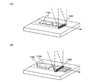
図1(A)に、第1のビームスポット901の形状と、該第1のビームスポット901
のみの走査により結晶化された半導体膜902の上面図と、第1のビームスポット901
の長軸方向において、半導体膜902に吸収されるレーザ光のエネルギーの分布とを示す
。なお半導体膜の結晶化は、白抜きの矢印で示すように、第1のビームスポット901を
長軸方向に対して垂直の方向に走査することで行なう。
FIG. 1A shows the shape of the
The top view of the
In the major axis direction, the energy distribution of laser light absorbed by the
図1(A)では第1のビームスポット901は矩形状であり、中心付近のある一定の範
囲においてそのエネルギーが一定の高さに保たれているが、例えば第1のビームスポット
の形状が楕円形状の場合は、エネルギー分布が正規曲線を描いている。いずれにしろ、第
1のビームスポット901のエネルギー分布は、通常エッジから中心に近くなるほど高く
なっている。そして、第1のビームスポット901のうち、半導体膜を溶融するのに必要
なエネルギーEAよりも高いエネルギーを有する領域と重なった部分において、半導体膜
902が結晶化されている。
In FIG. 1A, the
そして図1(A)に示すように、第1のビームスポット901のみによって結晶化され
た半導体膜902は、複数の結晶粒が集合して形成されている。その結晶粒の位置と大き
さはランダムであるが、第1のビームスポット901の中心に近くなるほどエネルギーが
高い(具体的にはエネルギーEBより高い)ので、該中心付近の領域903では半導体膜
が完全に溶融し、粒径約1μm程度の結晶粒が得られる傾向にある。逆に、エッジ近傍の
エネルギーの低い領域904(ここではエネルギーEB以下の領域)においては、部分的
に溶融しきれない領域が残ることで、中心付近の領域903ほど粒径の大きい結晶粒は得
られず、粒径の比較的小さい結晶粒(微結晶)のみが形成される傾向にある。なおエネル
ギーEBの高さはエネルギーEAよりも高く、第1のビームスポット901内の最も高いエ
ネルギーECよりも低い。
As shown in FIG. 1A, the
エッジ近傍の微結晶が形成される領域904は、粒界の欠陥に起因する再結合中心や捕
獲中心によってキャリアの電流輸送特性が低く、半導体素子として用いるのに適さない。
よって、微結晶が形成される領域904は狭い方が、半導体素子のレイアウトの制約を緩
和することができるので望ましい。しかし第1のビームスポット901内には、エネルギ
ーがEAより高くEBより低い領域が存在しているため、光学系の調整のみで微結晶が形成
される領域904を小さくするのには限界がある。
A
Therefore, it is preferable that the
次に図1(B)に、第1のビームスポット901及び第2のビームスポット911の形
状と、第1及び第2のビームスポット901、911を両方走査することにより結晶化さ
れた半導体膜912の上面図と、第1及び第2のビームスポット901、911の長軸方
向において、半導体膜912に吸収されるレーザ光のエネルギーの分布とを示す。なお半
導体膜912の結晶化は、白抜きの矢印で示すように、第1及び第2のビームスポット9
01、911を長軸方向に対して垂直の方向に走査することで行なう。
Next, FIG. 1B shows the shape of the
This is performed by scanning 01 and 911 in a direction perpendicular to the major axis direction.
図1(B)では、第2のビームスポット911が第1のビームスポット901を完全に
覆うように重なっている。波長が1μm程度の基本波は固相の半導体膜に殆ど吸収されな
いが、液相の半導体膜に対する吸収係数は固相の1000倍であり、吸収されやすい。よ
って図1(B)の場合、第1のビームスポット901のうち、半導体膜を溶融するのに必
要なエネルギーEAよりも高いエネルギーの領域においてのみ、基本波である第2のレー
ザ光のエネルギーが半導体膜に吸収される。このため図1(B)において実線で示すよう
に、半導体膜912に吸収されるレーザ光のトータルのエネルギーは、第1のレーザ光の
エネルギーがEAよりも高い領域において、不連続的に他の領域より高くなる。
In FIG. 1B, the
また第2のレーザ光は連続発振であるので、第1のレーザ光により溶融した部分が、連
続発振である第2のレーザ光の照射により、その溶融状態を維持したまま半導体膜中で移
動するので、走査方向に向かって連続的に成長した結晶粒が形成される。従って、半導体
膜912のうち、第1のビームスポット901の不連続的にエネルギーの高い領域があた
った部分に、大粒径の結晶粒を含む領域(大結晶領域)913を形成することができる。
具体的には、含まれる結晶粒の走査方向における幅が10〜30μm、走査方向に対して
垂直な方向における幅が1〜5μm程度の、大結晶領域913を形成することができる。
In addition, since the second laser light is continuous oscillation, the portion melted by the first laser light moves in the semiconductor film while maintaining the melted state by irradiation with the second laser light that is continuous oscillation. Therefore, crystal grains that are continuously grown in the scanning direction are formed. Accordingly, a region (large crystal region) 913 including crystal grains having a large grain size can be formed in a portion of the
Specifically, the
なお図1(B)の場合も図1(A)の場合と同様に、そのエッジ近傍に、大粒径の結晶
粒を含まず微結晶のみを含む領域914が形成される。この領域は、レーザ照射時におけ
る領域913からの熱伝導によって形成されるため完全に消滅させることはできないが、
レーザ光の照射条件を適切に選択することで、領域914を限りなく狭くすることができ
る。よって図1(A)の場合に比べ、大粒径の領域913の割合を高め、半導体素子のレ
イアウト上の制約を緩和することができる。
In the case of FIG. 1B as well, as in the case of FIG. 1A, a
By appropriately selecting the laser light irradiation conditions, the
また、図1(A)におけるエッジ近傍の微結晶が形成される領域904は、その表面に
半導体膜の膜厚と同程度の高さの凹凸(リッジ)が形成される。本実施例ではエッジ近傍
の微結晶が形成される領域を限りなく狭くすることができ、またリッジの高さを膜厚の半
分以下、より最適な条件下では4分の1以下とすることができる。例えば、半導体膜の膜
厚が100nmの場合、リッジの高さを50nm以下、より最適な条件下では20nm以
下程度とすることができ、より優れた特性の半導体素子を作製することができる。
In addition, in a
また、パルス発振のレーザ光のみで結晶化を行なった場合には、結晶の粒界において、
酸素、窒素、炭素等の不純物が偏析する傾向がある。レーザ光を用いた結晶化と触媒金属
を用いた結晶化とを組み合わせた場合は、ゲッタリングしきれなかった触媒金属が偏析す
ることがある。本発明では、第2のレーザ光により半導体膜に吸収されるレーザ光のトー
タルのエネルギーを高めることができるので、半導体膜が溶融してから固化するまでの時
間を長く保つことができる。よって帯域溶融法のごとく、偏析係数が正の不純物の偏析を
防ぎ、半導体膜の純化や溶質濃度の一様化を行なうことができる。したがって、該半導体
膜を用いた半導体素子の特性を高め、また特性のバラツキを抑えることができる。
In addition, when crystallization is performed only with pulsed laser light, at the crystal grain boundary,
Impurities such as oxygen, nitrogen, and carbon tend to segregate. When crystallization using laser light and crystallization using a catalyst metal are combined, the catalyst metal that could not be gettered may segregate. In the present invention, since the total energy of the laser light absorbed by the semiconductor film by the second laser light can be increased, the time from when the semiconductor film is melted to solidification can be kept long. Therefore, as in the zone melting method, segregation of impurities having a positive segregation coefficient can be prevented, and the semiconductor film can be purified and the solute concentration can be made uniform. Therefore, characteristics of a semiconductor element using the semiconductor film can be improved and variation in characteristics can be suppressed.
上述したように、第1のビームスポットと第2のビームスポットの大小関係によって、
得られる効果が異なる。最も望ましいのは、第2のビームスポットの形状に合わせ、第1
のビームスポットを第2のビームスポット内にぎりぎり収まる程度に最大限に大きくし、
究極的には2つのビームスポットを完全に重ね合わせることである。これにより、両者の
メリットを享受することができる。
As described above, depending on the magnitude relationship between the first beam spot and the second beam spot,
The effect obtained is different. Most preferably, the first beam is shaped according to the shape of the second beam spot.
The beam spot is maximized to fit within the second beam spot,
Ultimately, the two beam spots are completely superimposed. Thereby, both merit can be enjoyed.
また、連続発振の第2のビームスポットを複数連ね、それをパルス発振の第1のレーザ
光と重ねることで、大粒径の結晶が得られる領域の、走査方向に対して垂直な方向におけ
る幅をさらに広げることができる。またパルス発振の第1のビームスポットを連ねるよう
にしても良い。上記構成により、半導体素子のレイアウト上の制約をより緩和することが
でき、なおかつレーザ光の結晶化におけるスループットをより高めることができる。
Also, the width in the direction perpendicular to the scanning direction of the region where a crystal with a large grain size is obtained by connecting a plurality of continuous oscillation second beam spots and superimposing them with the pulse oscillation first laser beam. Can be further expanded. Further, the first beam spot of pulse oscillation may be connected. With the above configuration, restrictions on the layout of the semiconductor element can be relaxed, and the throughput in crystallization of laser light can be further increased.
なおビームスポットを線状とすることで、走査方向に結晶化された結晶粒が集まってい
る領域の、前記ビームスポットの長軸方向における幅を、できるだけ広くとることができ
る。つまり、長軸の両端に形成される結晶性の劣った領域の、全ビームスポットに占める
面積の割合を、低減させることができると言える。しかし本発明においてビームスポット
の形状は線状に限定されず、矩形状や面状であっても被照射体に対して十分なアニールを
行なえるのであれば問題はない。
By making the beam spot linear, the width of the beam spot in the major axis direction of the region where crystal grains crystallized in the scanning direction gather can be made as wide as possible. That is, it can be said that the ratio of the area occupied by all the beam spots in the region of poor crystallinity formed at both ends of the long axis can be reduced. However, in the present invention, the shape of the beam spot is not limited to a linear shape, and there is no problem even if it is rectangular or planar as long as sufficient annealing can be performed on the irradiated object.
なお第1のレーザ光は、パルス発振のArレーザ、Krレーザ、エキシマレーザ、CO2レ
ーザ、YAGレーザ、Y2O3レーザ、YVO4レーザ、YLFレーザ、YAlO3レーザ、ガラスレーザ、
ルビーレーザ、アレキサンドライトレーザ、Ti:サファイヤレーザ、銅蒸気レーザまたは
金蒸気レーザを用いることで得られる。
The first laser beam is a pulsed Ar laser, Kr laser, excimer laser, CO 2 laser, YAG laser, Y 2 O 3 laser, YVO 4 laser, YLF laser, YAlO 3 laser, glass laser,
It can be obtained by using a ruby laser, alexandrite laser, Ti: sapphire laser, copper vapor laser or gold vapor laser.
また第2のレーザ光は、連続発振のArレーザ、Krレーザ、CO2レーザ、YAGレーザ、Y2
O3レーザ、YVO4レーザ、YLFレーザ、YAlO3レーザ、アレキサンドライトレーザ、Ti:サフ
ァイヤレーザまたはヘリウムカドミウムレーザを用いることで得られる。
The second laser light is a continuous wave Ar laser, Kr laser, CO 2 laser, YAG laser, Y 2
It can be obtained by using O 3 laser, YVO 4 laser, YLF laser, YAlO 3 laser, alexandrite laser, Ti: sapphire laser or helium cadmium laser.
なお連続発振のレーザによる半導体膜の結晶化工程において、ビームスポットを一方向
に長い楕円状または矩形状に加工し、該ビームスポットの短軸方向に走査させて半導体膜
を結晶化させるとスループットを高めることができる。加工後のレーザビームの形状が楕
円状になるのは、元のレーザ光の形状が円形もしくはそれに近い形状であるからである。
レーザ光の元の形状が長方形状であれば、それをシリンドリカルレンズなどで1方向に拡
大することでさらに長軸がさらに長くなるように加工してから、用いても良い。また複数
のレーザビームをそれぞれ一方向に長い楕円状または矩形状に加工し、それらをつなげて
一方向にさらに長いビームを作って、スループットをより高めるようにしても良い。
Note that in the crystallization process of a semiconductor film using a continuous wave laser, the beam spot is processed into an elliptical or rectangular shape that is long in one direction, and the semiconductor film is crystallized by scanning in the short axis direction of the beam spot. Can be increased. The reason why the shape of the laser beam after processing is elliptical is that the shape of the original laser beam is circular or close to it.
If the original shape of the laser beam is a rectangular shape, it may be used after it has been processed so that the long axis is further elongated by enlarging it in one direction with a cylindrical lens or the like. In addition, a plurality of laser beams may be processed into an elliptical or rectangular shape that is long in one direction, and connected to create a longer beam in one direction, thereby further increasing the throughput.
本発明では、半導体膜に吸収されやすい可視光線以下の波長を有する、パルス発振の第
1のレーザ光を照射することで半導体膜を溶融し、基本波の吸収係数を高める。第1のレ
ーザ光をパルス発振とすることで、連続発振のときよりもビームスポットの面積を飛躍的
に広く取ることができる。そしてその溶融した状態で基本波を有する第2のレーザ光を照
射することで、基本波の吸収係数が高められた半導体膜に第2のレーザ光が効率良く吸収
される。よって、ビームスポットの長軸を長く取ることができるため、レーザ結晶化のス
ループットを高めることができ、またデザインルールの緩和に有効である。
In the present invention, the semiconductor film is melted by irradiation with pulsed first laser light having a wavelength of visible light or less that is easily absorbed by the semiconductor film, and the absorption coefficient of the fundamental wave is increased. By using pulse oscillation for the first laser beam, the area of the beam spot can be drastically increased compared to continuous oscillation. By irradiating the second laser light having the fundamental wave in the melted state, the second laser light is efficiently absorbed by the semiconductor film having an increased fundamental wave absorption coefficient. Therefore, since the long axis of the beam spot can be made long, the throughput of laser crystallization can be increased, and it is effective in relaxing the design rule.
また第1のレーザ光によって溶融し、吸収係数が高められた領域を、第2のレーザ光を
走査することで移動させることができ、該走査方向に結晶成長した結晶粒が敷き詰められ
た領域を形成することができる。さらに、第1のレーザ光の照射が途絶えた後も、その溶
融して吸収係数が高められた領域を、第2のレーザ光の走査によりある程度一方向に移動
させることができる。
Further, the region melted by the first laser beam and having an increased absorption coefficient can be moved by scanning the second laser beam, and the region in which crystal grains grown in the scanning direction are spread is provided. Can be formed. Furthermore, even after the irradiation of the first laser beam is interrupted, the region whose absorption coefficient is increased by melting can be moved to one direction to some extent by the scanning of the second laser beam.
また第2のレーザ光を基本波とすることで、高調波への変換に用いる非線形光学素子の
耐性を考慮する必要はなく、第2のレーザ光として、非常に大出力のレーザ、例えば高調
波の100倍以上のエネルギーのものを用いることができる。そして、非線形光学素子の
変質によるメンテナンスの煩雑さがなくなる。特に、メンテフリーの状態を長く保てると
いう固体レーザの利点を、生かすことができる。
Further, since the second laser beam is used as a fundamental wave, it is not necessary to consider the tolerance of the nonlinear optical element used for the conversion to the harmonic, and the second laser beam is a very high output laser, for example, a harmonic. Can be used having an energy of 100 times or more. And the maintenance complexity due to the alteration of the nonlinear optical element is eliminated. In particular, the advantage of a solid-state laser that can maintain a maintenance-free state for a long time can be utilized.
また第1のビームスポットと、第2のビームスポットとの走査方向を揃え、第1のビー
ムスポットが第2のビームスポット内に収まるようにすることで、課題を解決するための
手段において説明したように、ビームスポットのエッジ近傍における微結晶領域を、激減
させるかもしくは消滅させることができる。
Also, the means for solving the problem has been described by aligning the scanning directions of the first beam spot and the second beam spot so that the first beam spot is within the second beam spot. As described above, the microcrystalline region in the vicinity of the edge of the beam spot can be drastically reduced or eliminated.
(実施の形態1)
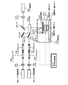
図3を用いて、本発明のレーザ照射装置の構成について説明する。
(Embodiment 1)
The configuration of the laser irradiation apparatus of the present invention will be described with reference to FIG.
101はパルス発振のレーザ発振器であり、本実施の形態では、6WのNd:YLFレーザを
用いる。レーザ発振器101は、TEM00の発振モードで、非線形光学素子により第2高
調波に変換されている。特に第2高調波に限定する必要はないがエネルギー効率の点で、
第2高調波の方が、さらに高次の高調波と比較して優れている。周波数は1kHz、パル
ス幅は60nsec程度である。本実施の形態では、出力が6W程度の固体レーザを使用する
が、出力が300Wに達するような大型レーザ、例えばXeCl、KrF、ArFエキシマレーザな
どを用いてもよい。例えばXeClエキシマレーザだと波長は308nm、KrFエキシ
マレーザだと波長248nmとなる。
The second harmonic is superior to higher harmonics. The frequency is 1 kHz and the pulse width is about 60 nsec. In this embodiment, a solid-state laser having an output of about 6 W is used, but a large-sized laser having an output reaching 300 W, such as an XeCl, KrF, or ArF excimer laser, may be used. For example, the wavelength is 308 nm for a XeCl excimer laser, and the wavelength is 248 nm for a KrF excimer laser.
なお非線形光学素子は、発振器が有する共振器内に設けていても良いし、基本波の共振
器の外に別途非線形光学素子を備えた共振器を設けていても良い。前者は装置が小型にな
り、共振器長の精密制御が不要になるという利点を有し、後者は基本波と高調波の相互作
用を無視できるという利点を有する。
The nonlinear optical element may be provided in a resonator included in the oscillator, or a resonator including a nonlinear optical element may be provided in addition to the fundamental wave resonator. The former has the advantage that the device becomes smaller and precise control of the resonator length becomes unnecessary, and the latter has the advantage that the interaction between the fundamental wave and the harmonic can be ignored.
非線形光学素子には、非線形光学定数の比較的大きいKTP(KTiOPO4)、BB
O(β−BaB2O4)、LBO(LiB3O5)、CLBO(CsLiB6O10)、GdY
COB(YCa4O(BO3)3)、KDP(KD2PO4)、KB5、LiNbO3、Ba2
NaNb5O15等の結晶が用いられており、特にLBOやBBO、KDP、KTP、KB
5、CLBO等を用いることで基本波から高調波への変換効率を高めることができる。
Nonlinear optical elements include KTP (KTiOPO 4 ), BB having a relatively large nonlinear optical constant.
O (β-BaB 2 O 4 ), LBO (LiB 3 O 5 ), CLBO (CsLiB 6 O 10 ), GdY
COB (YCa 4 O (BO 3 ) 3 ), KDP (KD 2 PO 4 ), KB5, LiNbO 3 , Ba 2
Crystals such as NaNb 5 O 15 are used, especially LBO, BBO, KDP, KTP, KB
5. By using CLBO or the like, the conversion efficiency from the fundamental wave to the harmonic can be increased.
レーザ光は通常水平方向に射出されることから、レーザ発振器101から発振された第
1のレーザ光は、反射ミラー102にて、鉛直方向からの角度(入射角)がθ1となる方
向に、その進行方向が変換される。本実施の形態では、θ1=21°とする。進行方向が
変換された第1のレーザ光は、レンズ103によりそのビームスポットの形状が加工され
、被処理物104に照射される。図3では、反射ミラー102とレンズ103とが第1の
レーザ光のビームスポットの形状及び位置を制御する光学系に相当する。
Since the laser light is normally emitted in the horizontal direction, the first laser light oscillated from the
図3では、レンズ103として平凹シリンドリカルレンズ103aと、平凸シリンドリ
カルレンズ103bを用いている。
In FIG. 3, as the
平凹シリンドリカルレンズ103aは、曲率半径10mm、厚さ2mmであり、第1の
レーザ光の進行方向を光軸としたときに、被処理物104の表面から光軸に沿って29m
mの位置に配置されている。そして平凹シリンドリカルレンズ103aの母線と被処理物
104に入射する第1のレーザ光の入射面とを垂直とする。
The plano-concave
It is arranged at the position of m. Then, the bus line of the plano-concave
平凸シリンドリカルレンズ103bは、曲率半径15mm、厚さ2mmであり、被処理
物104の表面から光軸に沿って24mmの位置に配置されている。そして平凸シリンド
リカルレンズ103bの母線は、被処理物104に入射する第1のレーザ光の入射面と平
行とする。
The plano-convex
これにより、被処理物104において3mm×0.2mmのサイズの第1のビームスポ
ット106が形成される。
As a result, a
また110は、連続発振のレーザ発振器であり、本実施の形態では2kW、基本波(波
長1064nm)のNd:YAGレーザを用いる。レーザ発振器110から発振された第2のレ
ーザ光は、φ300μmの光ファイバー111により伝送される。光ファイバー111は
、鉛直方向に対する射出口の向きが角度θ2となるように配置されている。本実施の形態
ではθ2=45°とする。また光ファイバー111の射出口は、レーザ発振器110から
射出する第2のレーザ光の光軸に沿って被処理物104から105mmの位置に配置され
ており、該光軸は入射面に含まれるようにする。
光ファイバー111から出射した第2のレーザ光は、レンズ112によりそのビームス
ポットの形状が加工され、被処理物104に照射される。図3では、光ファイバー111
とレンズ112とが第2のレーザ光のビームスポットの形状及び位置を制御する光学系に
相当する。
The shape of the beam spot of the second laser light emitted from the
And the
図3では、レンズ112として平凸シリンドリカルレンズ112aと、平凸シリンドリ
カルレンズ112bを用いている。
In FIG. 3, as the
平凸シリンドリカルレンズ112aは、曲率半径15mm、厚さ4mmであり、被処理
物104の表面から第2のレーザ光の光軸に沿って85mmの位置に配置されている。平
凸シリンドリカルレンズ112aの母線の方向は入射面と垂直とする。
The plano-convex
平凸シリンドリカルレンズ112bは、曲率半径10mm、厚さ2mmであり、被処理
物104の表面から第2のレーザ光の光軸に沿って25mmの位置に配置されている。
The planoconvex
これにより、被処理物104において、3mm×0.1mmのサイズの第2のビームス
ポット105が形成される。
As a result, a
本実施の形態では、被処理物104として半導体膜が成膜された基板を、水平面と平行
になるように設置する。半導体膜は例えば、ガラス基板の表面に成膜する。半導体膜が成
膜された基板は、厚さ0.7mmのガラス基板であり、レーザ照射の際に基板が落ちない
ように、吸着ステージ107に固定されている。
In this embodiment, a substrate over which a semiconductor film is formed as the object to be processed 104 is placed so as to be parallel to a horizontal plane. For example, the semiconductor film is formed on the surface of a glass substrate. The substrate on which the semiconductor film is formed is a glass substrate having a thickness of 0.7 mm, and is fixed to the
吸着ステージ107は、X軸用の一軸ロボット108とY軸用の一軸ロボット109に
より、被処理物104に平行な面内においてXY方向に移動が可能である。
The
なお、レーザ光に対して透光性を持つ基板上に成膜された半導体膜をアニールする場合
、均一なレーザ光の照射を実現するためには、照射面に垂直な平面であって、かつビーム
の形状を長方形と見立てたときの短辺を含む面または長辺を含む面のいずれか一方を入射
面と定義すると、前記レーザ光の入射角φは、入射面に含まれる前記短辺または前記長辺
の長さがW、前記照射面に設置され、かつ、前記レーザ光に対して透光性を有する基板の
厚さがdであるとき、φ≧arctan(W/2d)を満たすのが望ましい。複数のレーザ光を使用
する場合、この議論は個々のレーザ光について成り立つ必要がある。なお、レーザ光の軌
跡が、前記入射面上にないときは、該軌跡を該入射面に射影したときの入射角度をφとす
る。この入射角度φでレーザ光が入射されれば、基板の表面での反射光と、前記基板の裏
面からの反射光とが干渉せず、一様なレーザ光の照射を行なうことができる。以上の議論
は、基板の屈折率を1として考えた。実際は、基板の屈折率が1.5前後のものが多く、
この数値を考慮に入れると上記議論で算出した角度よりも大きな計算値が得られる。しか
しながら、ビームスポットのエネルギーはビームスポットの端に近づくに従い減衰がある
ため、この部分での干渉の影響は少なく、上記の算出値で十分に干渉減衰の効果が得られ
る。この議論は、第1のレーザ光に対しても、第2のレーザ光に対しても成り立ち両方と
も上記不等式を満たしているほうが好ましいが、エキシマレーザのように極端にコヒーレ
ント長の短いレーザに関しては、上記不等式を満たさなくても問題はない。上記のφに対
する不等式は、基板がレーザ光に対して透光性を有する場合にのみ適用される。
In the case of annealing a semiconductor film formed on a substrate that is transparent to laser light, in order to achieve uniform laser light irradiation, the plane is perpendicular to the irradiation surface, and When any one of a surface including a short side or a surface including a long side when the shape of the beam is regarded as a rectangle is defined as an incident surface, the incident angle φ of the laser beam is the short side included in the incident surface or Φ ≧ arctan (W / 2d) is satisfied when the length of the long side is W, the thickness of the substrate that is installed on the irradiation surface and has a light transmitting property to the laser beam is d. Is desirable. If multiple laser beams are used, this argument needs to hold for each laser beam. When the locus of the laser beam is not on the incident surface, the incident angle when the locus is projected onto the incident surface is φ. When laser light is incident at this incident angle φ, the reflected light from the surface of the substrate and the reflected light from the back surface of the substrate do not interfere with each other, and uniform laser light irradiation can be performed. In the above discussion, the refractive index of the substrate was considered as 1. Actually, many of the substrates have a refractive index of around 1.5,
Taking this value into consideration, a calculated value larger than the angle calculated in the above discussion can be obtained. However, since the energy of the beam spot is attenuated as it approaches the end of the beam spot, the influence of the interference in this portion is small, and the effect of interference attenuation can be sufficiently obtained by the above calculated value. It is preferable that both the first laser beam and the second laser beam satisfy the above inequality, but this discussion is about an extremely short coherent laser such as an excimer laser. There is no problem even if the above inequality is not satisfied. The above inequality for φ is applied only when the substrate is transparent to laser light.
一般に、ガラス基板は波長が1μm程度の基本波や緑色の第2高調波に対して透光性を
有する。本レンズが不等式を満たすためには、平凸シリンドリカルレンズ103bと平凸
シリンドリカルレンズ112bの位置を入射面と垂直な方向にずらしてビームスポットの
短軸を含む被処理物104の表面に垂直な面内において入射角度φ1、φ2を持たせれば
よい。この場合、第1のビームスポット106においては、φ1=10°、第2のビーム
スポット105においてはφ2=5°程度の傾きがあれば、干渉は起こらない。
Generally, a glass substrate has translucency with respect to a fundamental wave having a wavelength of about 1 μm or a green second harmonic. In order for this lens to satisfy the inequality, the planes of the planoconvex
なお第1のレーザ光と第2のレーザ光は、安定形共振器から得られるTEM00モード(
シングルモード)であることが望ましい。TEM00モードの場合、レーザ光はガウス形の
強度分布を持ち、集光性に優れているため、ビームスポットの加工が容易となる。
Note that the first laser beam and the second laser beam are TEM 00 modes (from a stable resonator).
Single mode) is desirable. In the case of the TEM 00 mode, the laser beam has a Gaussian intensity distribution and has excellent light collecting properties, so that the beam spot can be easily processed.
被処理物104として半導体膜が成膜された基板を用いる場合、例えば、厚さ0.7m
mのガラス基板の片面に、厚さ200nmの酸化窒化珪素を成膜し、その上に半導体膜と
して、厚さ70nmの非晶質珪素(a-Si)膜をプラズマCVD法を用いて成膜する。さらに
半導体膜のレーザに対する耐性を高めるために、500℃、1時間の熱アニールを該非晶
質珪素膜に対して行なう。熱アニールの他に、触媒金属を用いた結晶化を施していてもよ
い。熱アニールを施した半導体膜でも、触媒金属を用いて結晶化された半導体膜でも、最
適なレーザ光の照射条件はほぼ同様である。
When a substrate on which a semiconductor film is formed is used as the
A silicon oxynitride film having a thickness of 200 nm is formed on one surface of a glass substrate of m, and an amorphous silicon (a-Si) film having a thickness of 70 nm is formed thereon using a plasma CVD method as a semiconductor film. To do. Further, in order to increase the resistance of the semiconductor film to the laser, thermal annealing at 500 ° C. for 1 hour is performed on the amorphous silicon film. In addition to thermal annealing, crystallization using a catalytic metal may be performed. The optimum laser light irradiation conditions are substantially the same for both the semiconductor film subjected to thermal annealing and the semiconductor film crystallized using a catalytic metal.
そして、Y軸用の一軸ロボット109を用いて第2のビームスポット105の短軸方向
に、被処理物104(半導体膜が成膜された基板)を走査する。このとき各レーザ発振器
101、110の出力は仕様値とする。この被処理物104の走査により、第1のビーム
スポット106及び第2のビームスポット105が、被処理物104の表面に対して相対
的に走査されることになる。
Then, the workpiece 104 (the substrate on which the semiconductor film is formed) is scanned in the short axis direction of the
第1のビームスポット106が当たっている領域において半導体膜が溶融することで、
連続発振の第2のレーザ光の半導体膜への吸収係数が飛躍的に高まる。よって、走査方向
に延びた、第2のビームスポット105の長軸に相当する幅1mm〜2mmの領域に、該
走査方向に結晶成長した単結晶の結晶粒が敷き詰められた状態で形成される。
By melting the semiconductor film in the region where the
The absorption coefficient of the continuous wave second laser light into the semiconductor film is dramatically increased. Accordingly, single crystal grains grown in the scanning direction are formed in a state where the crystal growth in the scanning direction is spread over a region having a width of 1 mm to 2 mm corresponding to the long axis of the
なお半導体膜のうち、第1のビームスポット106及び第2のビームスポット105が
重なって照射される領域は、第2高調波の第1のレーザ光によって吸収係数が高められた
状態が、基本波である第2のレーザ光によって維持されていることになる。よって、たと
え第2高調波の第1のレーザ光の照射が途絶えたとしても、その後基本波である第2のレ
ーザ光によって、半導体膜が溶融して吸収係数が高められた状態が維持される。したがっ
て、第2高調波の第1のレーザ光の照射が途絶えた後も、その溶融して吸収係数が高めら
れた領域を、走査によりある程度一方向に移動させることができ、これにより走査方向に
向かって成長した結晶粒が形成されることとなる。そして、吸収係数が高められた領域を
、走査の過程において連続して維持しつづけるために、第2高調波の第1のレーザ光を再
び照射し、エネルギーを補充するのが望ましい。
Note that, in the semiconductor film, the region where the
なお第1のビームスポット106及び第2のビームスポット105の走査速度は、数c
m/s〜数百cm/s程度が適当であり、ここでは50cm/sとする。
The scanning speed of the
m / s to several hundreds cm / s is appropriate, and here it is 50 cm / s.
次に図4に、第1のビームスポット106及び第2のビームスポット105の、被処理
物104表面における走査経路を示す。被処理物104である半導体膜全面に第2のレー
ザ光を照射する場合、Y軸用の一軸ロボット109を用いて一方向への走査を行なった後
、X軸用の一軸ロボット108を用いて、Y軸用の一軸ロボット109による走査方向に
対して垂直の方向に、第1のビームスポット106及び第2のビームスポット105をス
ライドさせる。
Next, FIG. 4 shows a scanning path of the
例えば、Y軸用の一軸ロボット109により走査速度50cm/sにて、半導体膜を一
方向に走査する。図4において、該走査経路をA1で示す。次に、X軸用の一軸ロボット
108を用いて、走査経路をA1に対して垂直の方向に第1のビームスポット106及び
第2のビームスポット105をスライドさせる。該スライドによる走査経路をB1で示す
。次に、走査経路A1とは反対方向に向かって、Y軸用の一軸ロボット109により半導
体膜を一方向に走査する。該走査経路をA2で示す。次に、X軸用の一軸ロボット108
を用いて、走査経路をA2に対して垂直の方向に第1のビームスポット106及び第2の
ビームスポット105をスライドさせる。該スライドによる走査経路をB2で示す。この
ように、Y軸用の一軸ロボット109による走査とX軸用の一軸ロボット108による走
査とを順に繰り返すことで、被処理物104全面に第2のレーザ光または第1のレーザ光
を照射することができる。
For example, the semiconductor film is scanned in one direction by the Y-axis
Is used to slide the
なお、走査経路B1、B2…の長さは、第2のビームスポット105の長軸に相当する
幅1〜2mm分とするのが望ましい。
The lengths of the scanning paths B1, B2,... Are desirably set to a width of 1 to 2 mm corresponding to the long axis of the
第2のレーザ光が照射され、走査方向に成長した結晶粒が形成されている領域は、結晶
性に非常に優れている。そのため、該領域をTFTのチャネル形成領域に用いることで、
極めて高い移動度や、オン電流を期待できる。しかし半導体膜のうち、そのような高い結
晶性が必要とされない部分が存在する場合、該部分にはレーザ光を照射しないようにして
も良い。もしくは、走査の速度を増加させるなど、高い結晶性が得られないような条件で
レーザ光の照射を行なうようにしても良い。
A region where crystal grains grown in the scanning direction are irradiated with the second laser light is extremely excellent in crystallinity. Therefore, by using this region for the channel formation region of TFT,
Extremely high mobility and on-current can be expected. However, when there is a portion of the semiconductor film where such high crystallinity is not required, the portion may not be irradiated with laser light. Alternatively, laser light irradiation may be performed under conditions that do not provide high crystallinity, such as increasing the scanning speed.
なおレーザ光の走査は、被処理物である基板を固定してレーザ光の照射位置を移動させ
る照射系移動型と、レーザ光の照射位置を固定して基板を移動させる被処理物移動型と、
上記2つの方法を組み合わせた方法とがある。本発明のレーザ照射装置は、第1のレーザ
光と第2のレーザ光の少なくとも2つのレーザ光を用いるので、光学系の構成が最も単純
にすることができる被処理物移動型とするのが適している。しかし本発明のレーザ照射装
置はこれに限定されず、光学系を工夫することで、照射系移動型としたり、被処理物移動
型と照射系移動型を組み合わせたりすることも不可能ではない。いずれの場合においても
、各ビームスポットの半導体膜に対する相対的な移動方向を制御できることが前提である
。
The scanning of the laser beam includes an irradiation system moving type that fixes the substrate as the object to be processed and moves the irradiation position of the laser light, and an object movement type that fixes the irradiation position of the laser light and moves the substrate. ,
There is a method combining the above two methods. The laser irradiation apparatus of the present invention uses at least two laser beams of the first laser beam and the second laser beam, so that the object to be processed can be made to have the simplest optical system configuration. Is suitable. However, the laser irradiation apparatus of the present invention is not limited to this, and it is not impossible to make the irradiation system moving type by combining the optical system, or to combine the object moving type and the irradiation system moving type. In any case, it is assumed that the relative movement direction of each beam spot with respect to the semiconductor film can be controlled.
なお本発明のレーザ照射装置における、光学系は、本実施の形態で示した構成に限定さ
れない。
Note that the optical system in the laser irradiation apparatus of the present invention is not limited to the structure shown in this embodiment mode.
(実施の形態2)
次に図9を用いて、本発明のレーザ光の照射方法及び半導体装置の作製方法について説
明する。
(Embodiment 2)
Next, a laser light irradiation method and a semiconductor device manufacturing method of the present invention will be described with reference to FIGS.
まず図9(A)に示すように、基板500上に下地膜501を成膜する。基板500に
は、例えばバリウムホウケイ酸ガラスや、アルミノホウケイ酸ガラスなどのガラス基板、
石英基板、SUS基板等を用いることができる。また、PET、PES、PENに代表さ
れるプラスチックや、アクリル等の可撓性を有する合成樹脂からなる基板は、一般的に上
記基板と比較して耐熱温度が低い傾向にあるが、作製工程における処理温度に耐え得るの
であれば用いることが可能である。
First, as shown in FIG. 9A, a
A quartz substrate, a SUS substrate, or the like can be used. In addition, substrates made of plastics typified by PET, PES, PEN, and flexible synthetic resins such as acrylic generally tend to have lower heat-resistant temperatures than the above-mentioned substrates. Any material that can withstand the processing temperature can be used.
下地膜501は基板500中に含まれるNaなどのアルカリ金属やアルカリ土類金属が
、半導体膜中に拡散し、半導体素子の特性に悪影響を及ぼすのを防ぐために設ける。よっ
てアルカリ金属やアルカリ土類金属の半導体膜への拡散を抑えることができる酸化珪素や
、窒化珪素、窒化酸化珪素などの絶縁膜を用いて形成する。本実施の形態では、プラズマ
CVD法を用いて窒化酸化珪素膜を10nm〜400nm(好ましくは50nm〜300
nm)の膜厚になるように成膜した。
The
nm).
なお下地膜501は単層であっても複数の絶縁膜を積層したものであっても良い。また
ガラス基板、SUS基板またはプラスチック基板のように、アルカリ金属やアルカリ土類
金属が多少なりとも含まれている基板を用いる場合、不純物の拡散を防ぐという観点から
下地膜を設けることは有効であるが、石英基板など不純物の拡散がさして問題とならない
場合は、必ずしも設ける必要はない。
Note that the
次に下地膜501上に半導体膜502を形成する。半導体膜502の膜厚は25nm〜
100nm(好ましくは30nm〜60nm)とする。なお半導体膜502は、非晶質半
導体であっても良いし、多結晶半導体であっても良い。また半導体は珪素だけではなくシ
リコンゲルマニウムも用いることができる。シリコンゲルマニウムを用いる場合、ゲルマ
ニウムの濃度は0.01atomic%〜4.5atomic%程度であることが好ましい。
Next, a
100 nm (preferably 30 nm to 60 nm). Note that the
次に図9(B)に示すように、本発明のレーザ照射装置を用いて半導体膜502に第1
及び第2のレーザ光を照射し、結晶化を行なう。
Next, as shown in FIG. 9B, a first film is formed on the
Then, the second laser beam is irradiated to perform crystallization.
本実施の形態では第1のレーザ光として、エネルギー6W、1パルスのエネルギー6m
J/p、TEM00の発振モード、第2高調波(527nm)、発振周波数1kHz、パル
ス幅60nsecのYLFレーザを用いる。なお、第1のレーザ光を光学系により加工するこ
とで半導体膜502の表面に形成される第1のビームスポットは、短軸200μm、長軸
3mmの矩形状とし、エネルギー密度を1000mJ/cm2とする。
In this embodiment, as the first laser light, energy 6W, energy of 1 pulse 6m
A YLF laser having an oscillation mode of J / p, TEM 00, a second harmonic (527 nm), an oscillation frequency of 1 kHz, and a pulse width of 60 nsec is used. Note that the first beam spot formed on the surface of the
また本実施の形態では、第2のレーザ光としてエネルギー2kW、基本波(1.064
μm)のYAGレーザを用いる。なお、第2のレーザ光が発振されるレーザ発振器の出力
は、500W乃至5000Wであることが望ましい。第2のレーザ光を光学系により加工
することで半導体膜502の表面に形成される第2のビームスポットは、短軸100μm
、長軸3mmの矩形状とし、エネルギー密度を0.7MW/cm2とする。
In this embodiment mode, the second laser beam has an energy of 2 kW and a fundamental wave (1.064
μm) YAG laser. Note that the output of the laser oscillator that oscillates the second laser light is desirably 500 W to 5000 W. A second beam spot formed on the surface of the
The long axis is 3 mm and the energy density is 0.7 MW / cm 2 .
そして、半導体膜502の表面において、第1のビームスポットと第2のビームスポッ
トを重ね合わせるように照射し、上記2つのビームを図9(B)に示した白抜きの矢印の
方向に向かって走査する。第1のレーザ光により溶融することで、基本波の吸収係数が高
められ、第2のレーザ光のエネルギーが半導体膜に吸収されやすくなる。そして連続発振
である第2のレーザ光の照射により溶融した領域が半導体膜中で移動するので、走査方向
に向かって連続的に成長した結晶粒が形成される。該走査方向に沿って長く延びた単結晶
の粒を形成することで、少なくともTFTのチャネル方向には結晶粒界のほとんど存在し
ない半導体膜の形成が可能となる。
Then, irradiation is performed so that the first beam spot and the second beam spot are overlapped on the surface of the
なお、希ガスや窒素などの不活性ガス雰囲気中でレーザ光を照射するようにしても良い
。これにより、レーザ光照射による半導体表面の荒れを抑えることができ、界面準位密度
のばらつきによって生じる閾値のばらつきを抑えることができる。
Note that laser light may be irradiated in an inert gas atmosphere such as a rare gas or nitrogen. Thereby, roughness of the semiconductor surface due to laser light irradiation can be suppressed, and variation in threshold value caused by variation in interface state density can be suppressed.
上述した半導体膜502へのレーザ光の照射により、結晶性がより高められた半導体膜
503が形成される。
By irradiating the
次に、図9(C)に示すように半導体膜503をパターニングし、島状の半導体膜50
7〜509が形成され、該島状の半導体膜507〜509を用いてTFTに代表される各
種の半導体素子が形成される。
Next, as illustrated in FIG. 9C, the
7 to 509 are formed, and various semiconductor elements typified by TFTs are formed using the island-shaped
図示しないが、例えばTFTを作製する場合、次に島状の半導体膜507〜509を覆
うようにゲート絶縁膜を成膜する。ゲート絶縁膜には、例えば酸化珪素、窒化珪素または
窒化酸化珪素等を用いることができる。また成膜方法は、プラズマCVD法、スパッタ法
などを用いることができる。
Although not shown, for example, when a TFT is manufactured, a gate insulating film is formed so as to cover the island-shaped
次に、ゲート絶縁膜上に導電膜を成膜しパターニングすることでゲート電極を形成する
。そして、ゲート電極や、あるいはレジストを成膜しパターニングしたものをマスクとし
て用い、島状の半導体膜507〜509にn型またはp型の導電性を付与する不純物を添
加し、ソース領域、ドレイン領域、さらにはLDD領域等を形成する。
Next, a conductive film is formed over the gate insulating film and patterned to form a gate electrode. Then, a gate electrode or a resist film formed and patterned is used as a mask, an impurity imparting n-type or p-type conductivity is added to the island-shaped
上記一連の工程によってTFTを形成することができる。なお本発明の半導体装置の作
製方法は、島状の半導体膜の形成以降の、上述したTFTの作製工程に限定されない。本
発明のレーザ光の照射方法を用いて結晶化された半導体膜をTFTの活性層として用いる
ことで、素子間の移動度、閾値及びオン電流のばらつきを抑えることができる。
A TFT can be formed by the series of steps described above. Note that the method for manufacturing a semiconductor device of the present invention is not limited to the above-described TFT manufacturing process after the formation of an island-shaped semiconductor film. By using a semiconductor film crystallized by the laser light irradiation method of the present invention as an active layer of a TFT, variations in mobility, threshold value, and on-current between elements can be suppressed.
なお第1のレーザ光と第2のレーザ光は、本実施の形態で示した照射条件に限定されな
い。
Note that the first laser light and the second laser light are not limited to the irradiation conditions described in this embodiment mode.
例えば第1のレーザ光として、エネルギー4W、1パルスのエネルギー2mJ/p、T
EM00の発振モード、第2高調波(532nm)、発振周波数1kHz、パルス幅30ns
ecのYAGレーザを用いることもできる。また例えば、第1のレーザ光として、エネルギ
ー5W、1パルスのエネルギー0.25mJ/p、TEM00の発振モード、第3高調波(
355nm)、発振周波数20kHz、パルス幅30nsecのYVO4レーザを用いること
もできる。また例えば、第1のレーザ光として、エネルギー3.5W、1パルスのエネル
ギー0.233mJ/p、TEM00の発振モード、第4高調波(266nm)、発振周波
数15kHz、パルス幅30nsecのYVO4レーザを用いることもできる。
For example, as the first laser light,
EM 00 oscillation mode, second harmonic (532 nm),
An ec YAG laser can also be used. Further, for example, as the first laser beam, energy 5 W, pulse energy 0.25 mJ / p, TEM 00 oscillation mode, third harmonic (
355 nm), it is also possible to use oscillation frequency 20 kHz, a YVO 4 laser of a pulse width 30 nsec. For example, as the first laser beam, a YVO 4 laser having an energy of 3.5 W, an energy of one pulse of 0.233 mJ / p, an oscillation mode of TEM 00, a fourth harmonic (266 nm), an oscillation frequency of 15 kHz, and a pulse width of 30 nsec. Can also be used.
そして、第2のレーザ光として、例えばエネルギー500W、基本波(1.064μm
)のNd:YAGレーザを用いることができる。また例えば第2のレーザ光として、エネルギー
2000W、基本波(1.064μm)のNd:YAGレーザを用いることができる。
As the second laser beam, for example, energy 500 W, fundamental wave (1.064 μm
Nd: YAG laser can be used. For example, an Nd: YAG laser having an energy of 2000 W and a fundamental wave (1.064 μm) can be used as the second laser light.
また、レーザ光による結晶化の前に、触媒元素を用いた結晶化工程を設けても良い。触
媒元素としては、ニッケル(Ni)を用いているが、その以外にも、ゲルマニウム(Ge
)、鉄(Fe)、パラジウム(Pd)、スズ(Sn)、鉛(Pb)、コバルト(Co)、
白金(Pt)、銅(Cu)、金(Au)といった元素を用いることができる。触媒元素を
用いた結晶化工程の後に、レーザ光による結晶化工程を行なうと、触媒元素による結晶化
の際に形成された結晶が、基板により近い側においてレーザ光の照射により溶融されずに
残存し、該結晶を結晶核として結晶化が進む。よってレーザ光の照射による結晶化は基板
側から半導体膜の表面に向かって均一に進みやすく、レーザ光による結晶化工程のみの場
合に比べて、より半導体膜の結晶性を高めることができ、レーザ光による結晶化後の半導
体膜表面の荒れが抑えられる。よって後に形成される半導体素子、代表的にはTFTの特
性のばらつきがより抑えられ、オフ電流を抑えることができる。
Further, a crystallization step using a catalytic element may be provided before crystallization with laser light. Nickel (Ni) is used as the catalytic element, but besides that, germanium (Ge)
), Iron (Fe), palladium (Pd), tin (Sn), lead (Pb), cobalt (Co),
Elements such as platinum (Pt), copper (Cu), and gold (Au) can be used. When a crystallization process using a laser beam is performed after a crystallization process using a catalytic element, the crystal formed during the crystallization using the catalytic element remains on the side closer to the substrate without being melted by the laser beam irradiation. Then, crystallization proceeds using the crystal as a crystal nucleus. Therefore, crystallization by laser light irradiation tends to progress uniformly from the substrate side toward the surface of the semiconductor film, and the crystallinity of the semiconductor film can be improved more than in the case of only the crystallization process by laser light. The surface roughness of the semiconductor film after crystallization by light can be suppressed. Accordingly, variation in characteristics of semiconductor elements formed later, typically TFTs, can be further suppressed, and off-current can be suppressed.
なお、触媒元素を添加してから加熱処理を行なって結晶化を促進してから、レーザ光の
照射により結晶性をより高めていても良いし、加熱処理の工程を省略しても良い。具体的
には、触媒元素を添加してから加熱処理の代わりにレーザ光を照射し、結晶性を高めるよ
うにしても良い。
Note that after the catalyst element is added and heat treatment is performed to promote crystallization, the crystallinity may be further increased by laser light irradiation, or the heat treatment step may be omitted. Specifically, after adding a catalyst element, laser light may be irradiated instead of heat treatment to improve crystallinity.
なお本実施の形態では、半導体膜の結晶化に本発明のレーザ照射方法を用いた例を示し
たが、半導体膜にドーピングした不純物元素の活性化を行なうのに用いても良い。
Note that although an example in which the laser irradiation method of the present invention is used for crystallization of a semiconductor film is described in this embodiment mode, the semiconductor film may be used for activation of an impurity element doped.
本発明の半導体装置の作製方法は、集積回路や半導体表示装置の作製方法に用いること
ができる。特に、液晶表示装置、有機発光素子に代表される発光素子を各画素に備えた発
光装置、DMD(Digital Micromirror Device)、PDP(Plasma Display Panel)、F
ED(Field Emission Display)等の半導体表示装置の画素部に設けられたトランジスタ
等の半導体素子に用いた場合、画素部において照射されたレーザ光のエネルギーの分布に
起因する横縞が、視認されるのを抑えることができる。
The method for manufacturing a semiconductor device of the present invention can be used for a method for manufacturing an integrated circuit or a semiconductor display device. In particular, a liquid crystal display device, a light emitting device having a light emitting element typified by an organic light emitting element in each pixel, DMD (Digital Micromirror Device), PDP (Plasma Display Panel), F
When used in a semiconductor element such as a transistor provided in a pixel portion of a semiconductor display device such as an ED (Field Emission Display), horizontal stripes due to the energy distribution of laser light irradiated in the pixel portion are visually recognized. Can be suppressed.
本実施例では、本発明のレーザ照射装置の一形態について説明する。 In this embodiment, one mode of a laser irradiation apparatus of the present invention will be described.
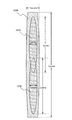
図5に本実施例のレーザ照射装置の構成を示す。本実施例では、パルス発振の可視光線
以下の波長を有する第1のレーザ光が、レーザ発振器1520から発振される。また連続
発振の第2のレーザ光が、2つのレーザ発振器1500、1501から発振されている。
FIG. 5 shows the configuration of the laser irradiation apparatus of this embodiment. In this embodiment, a first laser beam having a wavelength shorter than or equal to that of pulsed visible light is oscillated from a
なお本実施例では、レーザ発振器1520にエキシマレーザを用い、1パルスあたりの
出力エネルギーを1J、パルス幅を30nsec程度、従って単位時間あたりの出力を30M
Wとする。またレーザ発振器1500、1501には共にYAGレーザを用い、それぞれ
出力エネルギーを10kWとする。
In this embodiment, an excimer laser is used as the
W. The laser oscillators 1500 and 1501 are both YAG lasers, and each output energy is 10 kW.
レーザ発振器1520から発振される第1のレーザ光は、ミラー1523において反射
された後、光学系1524において矩形状、楕円形状または線状に集光され、被処理物1
514に照射される。なお本実施例では、レーザ発振器1520とミラー1523との間
に、第1のレーザ光を遮るシャッター1521が設けられているが、必ずしも設ける必要
はない。また光学系1524は、線状、矩形状または楕円形状にビームスポットを集光し
、エネルギー分布を均一にできるものであれば良い。
The first laser light oscillated from the
514 is irradiated. In this embodiment, the
一方、レーザ発振器1500、1501から発振された第2のレーザ光は、それぞれビ
ームエキスパンダー1508、1560に入射する。本実施例では、レーザ発振器150
0、1501とビームエキスパンダー1508、1560との間に、第2のレーザ光を遮
るシャッター1502、1503がそれぞれ設けられているが、必ずしも設ける必要はな
い。
On the other hand, the second laser light oscillated from the laser oscillators 1500 and 1501 enters the
そして、ビームエキスパンダー1508、1560によって、入射してきた第2のレー
ザ光の広がりを抑え、なおかつ、ビームの断面形状の大きさを調整することができる。
The
ビームエキスパンダー1508、1560から出射した第2のレーザ光は、シリンドリ
カルレンズ1509、1561において、そのビームの断面形状が矩形状、楕円形状また
は線状になるようにそれぞれ伸長される。そして、該伸長された第2のレーザ光は、ミラ
ー1510、1562においてそれぞれ反射し、共にレンズ1511に入射する。入射し
たレーザ光はレンズ1511によって線状に集光され、レーザ照射室1513内の被処理
物1514に照射される。本実施例ではレンズ1511としてシリンドリカルレンズを用
いたが、ビームスポットを矩形状、楕円形状または線状にすることができるレンズであれ
ば良い。
The second laser beams emitted from the
本実施例においては、ミラー1523、光学系1524が第1のレーザ光に対応する光
学系に相当する。またビームエキスパンダー1508、1560、シリンドリカルレンズ
1509、1561、ミラー1510、1562が、第2のレーザ光に対応する光学系に
相当する。これら2つの光学系によって、第1のレーザ光により被処理物1514の表面
に形成される第1のビームスポットと、第2のレーザ光により被処理物1514の表面に
形成される第2のビームスポットとを重ね合わせることができる。
In this embodiment, the mirror 1523 and the
図7に、図5に示すレーザ照射装置において用いられる各ビームスポットの形状及びそ
の配置の一例を示す。図7において、1570は第1のビームスポットに相当し、157
1、1572はそれぞれ第2のビームスポットに相当する。図7では、第2のビームスポ
ット1571と1572を、その長軸が一致するように、互いに一部重ね合わされている
。そして、第2のビームスポット1571、1572を完全に覆うように、第1のビーム
スポット1570が重なっている。
FIG. 7 shows an example of the shape and arrangement of each beam spot used in the laser irradiation apparatus shown in FIG. In FIG. 7, 1570 corresponds to the first beam spot, and 157
本実施例では、第1のビームスポット1570の短軸方向の長さLX1570を400μm
、長軸方向の長さLY1570を110mmとし、エネルギー密度を25MW/cm2程度とす
る。1パルスあたりのエネルギー密度に換算すると100〜1000mJ/cm2程度が
適当である。また第2のビームスポット1572の短軸方向の長さLX1572を200μm
、長軸方向の長さLY1572を60mmとし、エネルギー密度を0.1MW/cm2とする。
そして第2のビームスポット1571、1572は、互いに20mm分重なっており、第
2のビームスポット1571、1572の長軸を連ねた長さが100mmとなるようにす
る。
In this embodiment, the length L X1570 in the minor axis direction of the
The length L Y1570 in the major axis direction is set to 110 mm, and the energy density is set to about 25 MW / cm 2 . When converted to the energy density per pulse, about 100 to 1000 mJ / cm 2 is appropriate. The length L X1572 in the minor axis direction of the
The length L Y1572 in the major axis direction is 60 mm, and the energy density is 0.1 MW / cm 2 .
The
このように第2のレーザ光を複数合成することで、第1のレーザ光と第2のレーザ光が
重なる領域を広げることができ、レーザ光が照射された領域全体に占める、該結晶性の劣
っている領域の割合を減らすことができる。
By combining a plurality of second laser beams in this way, the region where the first laser beam and the second laser beam overlap can be expanded, and the crystalline property occupies the entire region irradiated with the laser beam. The ratio of inferior areas can be reduced.
なお本実施例では2つのレーザ発振器を用いて、2系統の第2のレーザ光を被処理物に
照射しているが、本発明はこれに限定されず、3以上の複数の系統の第2のレーザ光を用
いるようにしても良い。また第1のレーザ光も複数の系統としても良い。
In this embodiment, two laser oscillators are used to irradiate the object to be processed with the two systems of the second laser light. However, the present invention is not limited to this, and the second system of the three or more systems is used. The laser beam may be used. The first laser light may also be a plurality of systems.
レーザ照射室1513内において、被処理物1514はステージ1515上に載置され
ており、該ステージ1515は3つの一軸ロボット1516〜1518によってその位置
が制御されている。具体的には、φ軸用の一軸ロボット1516により、水平面内におい
てステージ1515を回転させることができる。また、X軸用の一軸ロボット1517に
より、水平面内においてステージ1515をX軸方向に移動させることができる。また、
Y軸用の一軸ロボット1518により、水平面内においてステージ1515をY軸方向に
移動させることができる。各位置制御手段の動作は、中央処理装置1519において制御
されている。
In the
The stage 1515 can be moved in the Y-axis direction in the horizontal plane by the single-
Y軸方向に長く伸ばされた線状のビームスポットを照射しながら被処理物をX方向に走
査させることで、走査方向に沿って長く伸びた結晶粒の集まりを形成できる。走査の速度
は例えば10〜2000mm/s、好ましくは100〜1000mm/sとすれば良いが
、半導体膜の膜厚、材料等の条件により、走査速度の最適な範囲は前後する。これにより
、走査方向に延びた幅100mmの領域に、該走査方向に結晶成長した単結晶の結晶粒を
敷き詰めるように形成することができる。この走査方向に結晶成長した結晶粒が敷き詰め
られた領域は、単に連続発振のレーザ光のみを用いて結晶化を行なう従来技術の場合と比
較して、その幅が100倍程度と飛躍的に広い。
By irradiating the object to be processed in the X direction while irradiating a linear beam spot elongated in the Y-axis direction, a collection of crystal grains elongated in the scanning direction can be formed. The scanning speed may be, for example, 10 to 2000 mm / s, preferably 100 to 1000 mm / s. However, the optimum range of the scanning speed varies depending on conditions such as the film thickness and material of the semiconductor film. Thereby, it is possible to form a single crystal crystal grain that has grown in the scanning direction in a region having a width of 100 mm extending in the scanning direction. The region where the crystal grains grown in the scanning direction are spread is dramatically widened by about 100 times as compared with the case of the conventional technique in which crystallization is performed using only continuous wave laser light. .
なお本実施例のように、CCD等の受光素子を用いたモニター1512を設け、被処理
物1514の位置を正確に把握できるようにしても良い。
Note that, as in this embodiment, a monitor 1512 using a light receiving element such as a CCD may be provided so that the position of the
図6を用いて、本発明のレーザ照射装置を用いて形成される半導体装置の1つである、
発光装置の画素の構成について説明する。
FIG. 6 shows one of semiconductor devices formed using the laser irradiation apparatus of the present invention.
A structure of a pixel of the light emitting device will be described.
図6において、基板6000に、下地膜6001が形成されており、該下地膜6001
上にトランジスタ6002が形成されている。トランジスタ6002は活性層6003と
、ゲート電極6005と、活性層6003とゲート電極6005の間に挟まれたゲート絶
縁膜6004と、を有している。
In FIG. 6, a
A
活性層6003は、本発明のレーザ照射装置を用いることで結晶化された多結晶半導体
膜が用いられている。なお、活性層は珪素だけではなくシリコンゲルマニウムを用いるよ
うにしても良い。シリコンゲルマニウムを用いる場合、ゲルマニウムの濃度は0.01〜
4.5atomic%程度であることが好ましい。また窒化炭素が添加された珪素を用いていて
も良い。
As the
It is preferably about 4.5 atomic%. Further, silicon to which carbon nitride is added may be used.
またゲート絶縁膜6004は、酸化珪素、窒化珪素または酸化窒化珪素を用いることが
できる。またそれらを積層した膜、例えばSiO2上にSiNを積層した膜を、ゲート絶
縁膜として用いても良い。またゲート電極6005として、Ta、W、Ti、Mo、Al
、Cuから選ばれた元素、または前記元素を主成分とする合金材料もしくは化合物材料で
形成する。また、リン等の不純物元素をドーピングした多結晶シリコン膜に代表される半
導体膜を用いてもよい。また単層の導電膜ではなく、複数の層からなる導電膜を積層した
ものであっても良い。
For the
, An element selected from Cu, or an alloy material or a compound material containing the element as a main component. Alternatively, a semiconductor film typified by a polycrystalline silicon film doped with an impurity element such as phosphorus may be used. Further, instead of a single conductive film, a conductive film composed of a plurality of layers may be stacked.
またトランジスタ6002は、第1の層間絶縁膜6006で覆われており、第1の層間
絶縁膜6006上には第2の層間絶縁膜6007と、第3の層間絶縁膜6008とが積層
されている。第1の層間絶縁膜6006は、プラズマCVD法またはスパッタ法を用い、
酸化珪素、窒化珪素または酸化窒化珪素膜を単層でまたは積層して用いることができる。
The
A silicon oxide film, a silicon nitride film, or a silicon oxynitride film can be used as a single layer or a stacked layer.
また第2の層間絶縁膜6007は、有機樹脂膜、無機絶縁膜、シロキサン系材料を出発
材料として形成されたSi−O結合とSi−CHx結合手を含む絶縁膜等を用いることが
できる。本実施例では非感光性のアクリルを用いる。第3の層間絶縁膜6008は、水分
や酸素などの発光素子の劣化を促進させる原因となる物質を、他の絶縁膜と比較して透過
させにくい膜を用いる。代表的には、例えばDLC膜、窒化炭素膜、RFスパッタ法で形
成された窒化珪素膜等を用いるのが望ましい。
As the second
また図6において6010は陽極、6011は電界発光層、6012は陰極であり、陽
極6010と電界発光層6011と陰極6012が重なっている部分が発光素子6013
に相当する。トランジスタ6002の一つは、発光素子6013に供給する電流を制御す
る駆動用トランジスタであり、発光素子6013と直接、または他の回路素子を介して直
列に接続されている。電界発光層6011は、発光層単独かもしくは発光層を含む複数の
層が積層された構成を有している。
In FIG. 6,
It corresponds to. One of the
陽極6010は第3の層間絶縁膜6008上に形成されている。また第3の層間絶縁膜
6008上には隔壁として用いる有機樹脂膜6014が形成されている。なお本実施例で
は隔壁として有機樹脂膜を用いているが、無機絶縁膜、シロキサン系材料を出発材料とし
て形成されたSi−O結合とSi−CHx結合手を含む絶縁膜等を隔壁として用いること
ができる。有機樹脂膜6014は開口部6015を有しており、該開口部において陽極6
010と電界発光層6011と陰極6012が重なり合うことで発光素子6013が形成
されている。
The
A
そして有機樹脂膜6014及び陰極6012上に、保護膜6016が成膜されている。
保護膜6016は第3の層間絶縁膜6008と同様に、水分や酸素などの発光素子の劣化
を促進させる原因となる物質を、他の絶縁膜と比較して透過させにくい膜、例えばDLC
膜、窒化炭素膜、RFスパッタ法で形成された窒化珪素膜等を用いる。
A
As with the third
A film, a carbon nitride film, a silicon nitride film formed by an RF sputtering method, or the like is used.
また有機樹脂膜6014の開口部6015における端部は、有機樹脂膜6014上に一
部重なって形成されている電界発光層6011に、該端部において穴があかないように、
丸みを帯びさせることが望ましい。具体的には、開口部における有機樹脂膜の断面が描い
ている曲線の曲率半径が、0.2〜2μm程度であることが望ましい。上記構成により、
後に形成される電界発光層や陰極のカバレッジを良好とすることができ、陽極6010と
陰極6012が電界発光層6011に形成された穴においてショートするのを防ぐことが
できる。また電界発光層6011の応力を緩和させることで、発光領域が減少するシュリ
ンクとよばれる不良を低減させることができ、信頼性を高めることができる。
In addition, the end of the
It is desirable to make it round. Specifically, it is desirable that the radius of curvature of the curve drawn by the cross section of the organic resin film in the opening is about 0.2 to 2 μm. With the above configuration,
The coverage of the electroluminescent layer and the cathode to be formed later can be improved, and the
なお図6では、有機樹脂膜6014として、ポジ型の感光性のアクリル樹脂を用いた例
を示している。感光性の有機樹脂には、光、電子、イオンなどのエネルギー線が露光され
た箇所が除去されるポジ型と、露光された箇所が残るネガ型とがある。本発明ではネガ型
の有機樹脂膜を用いても良い。また感光性のポリイミドを用いて有機樹脂膜6014を形
成しても良い。ネガ型のアクリルを用いて有機樹脂膜6014を形成した場合、開口部6
015における端部が、S字状の断面形状となる。このとき開口部の上端部及び下端部に
おける曲率半径は、0.2〜2μmとすることが望ましい。
Note that FIG. 6 illustrates an example in which a positive photosensitive acrylic resin is used as the
The end portion at 015 has an S-shaped cross-sectional shape. At this time, it is desirable that the radius of curvature at the upper end and the lower end of the opening is 0.2 to 2 μm.
陽極6010は透明導電膜を用いることができる。ITOの他、酸化インジウムに2〜
20%の酸化亜鉛(ZnO)を混合した透明導電膜を用いても良い。図6では陽極601
0としITOを用いている。また陰極6012は、仕事関数の小さい導電膜であれば公知
の他の材料を用いることができる。例えば、Ca、Al、CaF、MgAg、AlLi等
が望ましい。
A transparent conductive film can be used for the
A transparent conductive film mixed with 20% zinc oxide (ZnO) may be used. In FIG. 6, the anode 601
0 is used and ITO is used. The
なお図6では、発光素子から発せられる光が基板6000側に照射される構成を示して
いるが、光が基板とは反対側に向かうような構造の発光素子としても良い。また図6では
トランジスタ6002と発光素子の陽極6010が接続されているが、本発明はこの構成
に限定されず、トランジスタ6002と発光素子の陰極6012が接続されていても良い
。この場合、陰極は第3の層間絶縁膜6008上に形成される。そしてTiN等を用いて
形成される。
Note that FIG. 6 illustrates a structure in which light emitted from the light-emitting element is emitted to the
なお、実際には図6まで完成したら、さらに外気に曝されないように気密性が高く、脱
ガスの少ない保護フィルム(ラミネートフィルム、紫外線硬化樹脂フィルム等)や透光性
のカバー材でパッケージング(封入)することが好ましい。その際、カバー材の内部を不
活性雰囲気にしたり、内部に吸湿性材料(例えば酸化バリウム)を配置したりするとOL
EDの信頼性が向上する。
Actually, when completed up to FIG. 6, packaging with a protective film (laminate film, ultraviolet curable resin film, etc.) or a translucent cover material that is highly airtight and less degassed so as not to be exposed to the outside air ( (Encapsulation) is preferable. At that time, if the inside of the cover material is made an inert atmosphere, or a hygroscopic material (for example, barium oxide) is arranged inside, OL
ED reliability is improved.
なお、本実施例では半導体装置の一例として発光装置を例に挙げたが、本発明の作製方
法を用いて形成される半導体装置はこれに限定されない。
Note that although a light-emitting device is described as an example of a semiconductor device in this embodiment, a semiconductor device formed using the manufacturing method of the present invention is not limited thereto.
本実施例では実施の形態2とは異なり、本発明のレーザ照射装置による結晶化方法に、
触媒元素による結晶化方法を組み合わせた例について説明する。
In this example, unlike Embodiment 2, the crystallization method by the laser irradiation apparatus of the present invention is used.
The example which combined the crystallization method by a catalyst element is demonstrated.
まず、半導体膜502を成膜し、該半導体膜502に0族の元素のドーピングを行なう
工程まで、実施の形態2の図9(A)までを参照して行なう。次に図10(A)に示すよ
うに、半導体膜502の表面に、重量換算で1〜100ppmのNiを含む酢酸ニッケル
塩溶液をスピンコート法で塗布した。なお触媒の添加は上記方法に限定されず、スパッタ
法、蒸着法、プラズマ処理などを用いて添加しても良い。そして、500〜650℃で4
〜24時間、例えば570℃、14時間の加熱処理を行った。この加熱処理により、酢酸
ニッケル塩溶液が塗布された表面から、基板500に向かって縦方向に結晶化が促進され
た半導体膜520が形成される(図10(A))。
First, a process up to the step of forming a
The heat treatment was performed for -24 hours, for example, 570 ° C. for 14 hours. By this heat treatment, a
加熱処理には、例えば、ランプの輻射を熱源としたRTA(Rapid Thermal Anneal)、又
は加熱された気体を用いるRTA(ガスRTA)で設定加熱温度740℃、180秒のR
TAを行なう。設定加熱温度は、パイロメータで測る基板の温度であり、その温度を熱処
理時の設定温度としている。他の方法としては、ファーネスアニール炉を用いて550℃
にて4時間の熱処理があり、これを用いても良い。結晶化温度の低温化及び時短化は触媒
作用のある金属元素の作用によるものである。
For the heat treatment, for example, RTA (Rapid Thermal Anneal) using the radiation of the lamp as a heat source, or RTA (gas RTA) using a heated gas, a set heating temperature of 740 ° C., R for 180 seconds.
Perform TA. The set heating temperature is the temperature of the substrate measured with a pyrometer, and this temperature is set as the set temperature during heat treatment. Another method is to use a furnace annealing furnace at 550 ° C.
There is a heat treatment for 4 hours, and this may be used. The lowering and shortening of the crystallization temperature is due to the action of a catalytic metal element.
なお、本実施例では触媒元素としてニッケル(Ni)を用いているが、その以外にも、
ゲルマニウム(Ge)、鉄(Fe)、パラジウム(Pd)、スズ(Sn)、鉛(Pb)、
コバルト(Co)、白金(Pt)、銅(Cu)、金(Au)といった元素を用いても良い
。
In this example, nickel (Ni) is used as the catalyst element.
Germanium (Ge), iron (Fe), palladium (Pd), tin (Sn), lead (Pb),
Elements such as cobalt (Co), platinum (Pt), copper (Cu), and gold (Au) may be used.
次に図10(B)に示すように、半導体膜520を本発明のレーザ照射装置を用いて結
晶化する。本実施例では、第1のレーザ光として、1パルスあたりのエネルギー1J程度
、周波数300kHz、パルス幅25nsec程度のパルス発振のエキシマレーザを用い、ま
た第2のレーザ光としてエネルギー500W、基本波(1.064μm)のNd:YAGレーザ
を用いた。
Next, as shown in FIG. 10B, the
そして本実施例では、第1のレーザ光によって得られる第1のビームスポットと、第2
のレーザ光によって得られる第2のビームスポットとの走査方向を揃え、第1のビームス
ポットが第2のビームスポット内に収まるようにする。なおビームスポットの大小関係は
本実施例で示した構成に限定されない。本実施例のように、第2のビームスポットの方が
第1のビームスポットに比べて広くなるようにすることで、課題を解決するための手段に
おいて説明したように、ビームスポットのエッジ近傍における微結晶領域を、激減させる
かもしくは消滅させることができる。また逆に、該幅を、第1のビームスポットの方が第
2のビームスポットに比べて広くなるようにすることで、2つのレーザ光の重なる領域を
最大限に確保することができる。なお光学系による調整が可能であるならば、2つのビー
ムスポットの、走査方向に対して垂直の方向における幅を揃えることで、両方のメリット
を得ることができる。
In this embodiment, the first beam spot obtained by the first laser beam,
The scanning direction with the second beam spot obtained by the laser beam is aligned so that the first beam spot falls within the second beam spot. The magnitude relationship between the beam spots is not limited to the configuration shown in this embodiment. As described in the means for solving the problem, by making the second beam spot wider than the first beam spot as in the present embodiment, in the vicinity of the edge of the beam spot. The microcrystalline region can be drastically reduced or eliminated. Conversely, by making the width wider for the first beam spot than for the second beam spot, it is possible to maximize the region where the two laser beams overlap. If adjustment by the optical system is possible, both merits can be obtained by aligning the widths of the two beam spots in the direction perpendicular to the scanning direction.
上述した半導体膜520へのレーザ光の照射により、結晶性がより高められた半導体膜
521が形成される。なお、触媒元素を用いて結晶化された半導体膜521内には、触媒
元素(ここではNi)がおおよそ1×10¹⁹atoms/cm3程度の濃度で含まれていると考え
られる。次に、半導体膜521内に存在する触媒元素のゲッタリングを行なう。
By irradiating the
まず、図10(C)に示すように半導体膜521の表面に酸化膜522を形成する。1
nm〜10nm程度の膜厚を有する酸化膜522を形成することで、後のエッチング工程
において半導体膜521の表面がエッチングにより荒れるのを防ぐことができる。酸化膜
522は公知の方法を用いて形成することができる。例えば、硫酸、塩酸、硝酸などと過
酸化水素水を混合させた水溶液や、オゾン水で、半導体膜521の表面を酸化することで
形成しても良いし、酸素を含む雰囲気中でのプラズマ処理や、加熱処理、紫外線照射等に
より形成しても良い。また酸化膜を別途、プラズマCVD法やスパッタ法、蒸着法などで
形成しても良い。
First, as illustrated in FIG. 10C, an
By forming the
次に酸化膜522上に、希ガス元素を1×10²⁰atoms/cm3以上の濃度で含むゲッタリ
ング用の半導体膜523を、スパッタ法を用いて25〜250nmの厚さで形成する。ゲ
ッタリング用の半導体膜523は、半導体膜521とエッチングの選択比を大きくするた
め、半導体膜521よりも膜の密度の低い方がより望ましい。希ガス元素としてはヘリウ
ム(He)、ネオン(Ne)、アルゴン(Ar)、クリプトン(Kr)、キセノン(Xe
)から選ばれた一種または複数種を用いる。
Next, a
1 type or multiple types selected from.
次にファーネスアニール法やRTA法を用いて加熱処理を施し、ゲッタリングを行なう
。ファーネスアニール法で行なう場合には、窒素雰囲気中にて450〜600℃で0.5
〜12時間の加熱処理を行なう。また、RTA法を用いる場合には、加熱用のランプ光源
を1〜60秒、好ましくは30〜60秒点灯させ、それを1〜10回、好ましくは2〜6
回繰り返す。ランプ光源の発光強度は任意なものとするが、半導体膜が瞬間的には600
〜1000℃、好ましくは700〜750℃程度にまで加熱されるようにする。
Next, heat treatment is performed using a furnace annealing method or an RTA method to perform gettering. When the furnace annealing method is used, 0.5 to 450 ° C. to 600 ° C. in a nitrogen atmosphere.
Heat treatment for ˜12 hours. When the RTA method is used, the lamp light source for heating is turned on for 1 to 60 seconds, preferably 30 to 60 seconds, and it is turned on 1 to 10 times, preferably 2 to 6 times.
Repeat once. The emission intensity of the lamp light source is arbitrary, but the semiconductor film is instantaneously 600
It is made to heat to about -1000 degreeC, Preferably it is about 700-750 degreeC.
加熱処理により、半導体膜521内の触媒元素が、拡散により矢印に示すようにゲッタ
リング用の半導体膜523に移動し、ゲッタリングされる。
By the heat treatment, the catalytic element in the
次にゲッタリング用の半導体膜523を選択的にエッチングして除去する。エッチング
は、ClF3によるプラズマを用いないドライエッチング、或いはヒドラジンや、テトラ
エチルアンモニウムハイドロオキサイド((CH3)4NOH)を含む水溶液などアルカリ
溶液によるウエットエッチングで行なうことができる。この時酸化膜522によって半導
体膜521がエッチングされるのを防ぐことができる。
Next, the
次に酸化膜522をフッ酸により除去した後、半導体膜521をパターニングし、島状
の半導体膜524〜526を形成する(図10(D))。該島状の半導体膜524〜52
6を用いてTFTに代表される各種の半導体素子を形成することができる。なお、本発明
においてゲッタリング工程は、本実施例に示した方法に限定されない。その他の方法を用
いて半導体膜中の触媒元素を低減するようにしても良い。
Next, after the
6 can be used to form various semiconductor elements typified by TFTs. In the present invention, the gettering step is not limited to the method shown in this embodiment. Other methods may be used to reduce the catalytic element in the semiconductor film.
本実施例の場合、触媒元素による結晶化の際に形成された結晶が、基板により近い側に
おいてレーザ光の照射により溶融されずに残存し、該結晶を結晶核として結晶化が進む。
よってレーザ光の照射による結晶化は基板側から表面に向かって均一に進みやすく、また
その結晶方位を揃えやすいため、実施の形態2の場合に比べて表面の荒れが抑えられる。
よって後に形成される半導体素子、代表的にはTFTの特性のばらつきがより抑えられる
。
In the case of this example, the crystal formed during the crystallization with the catalytic element remains unmelted by laser light irradiation on the side closer to the substrate, and the crystallization proceeds using the crystal as a crystal nucleus.
Therefore, crystallization by laser light irradiation easily proceeds uniformly from the substrate side toward the surface, and the crystal orientation thereof is easily aligned, so that surface roughness can be suppressed as compared with the case of the second embodiment.
Therefore, variations in characteristics of semiconductor elements formed later, typically TFTs, can be further suppressed.
なお本実施例では、触媒元素を添加してから加熱処理を行なって結晶化を促進してから
、レーザ光の照射により結晶性をより高めている構成について説明した。本発明はこれに
限定されず、加熱処理の工程を省略しても良い。具体的には、触媒元素を添加してから加
熱処理の代わりにレーザ光を照射し、結晶性を高めるようにしても良い。
Note that in this embodiment, the structure in which the crystallinity is further enhanced by laser light irradiation after the catalyst element is added and then heat treatment is performed to promote crystallization has been described. The present invention is not limited to this, and the heat treatment step may be omitted. Specifically, after adding a catalyst element, laser light may be irradiated instead of heat treatment to improve crystallinity.
本実施例では、本発明のレーザ照射装置による結晶化方法に触媒元素による結晶化方法
を組み合わせた、実施例3とは異なる例について説明する。
In this example, an example different from Example 3 in which the crystallization method using the laser irradiation apparatus of the present invention is combined with the crystallization method using a catalytic element will be described.
まず、半導体膜502を成膜し、該半導体膜502に0族の元素のドーピングを行なう
工程まで、実施の形態2の図9(A)までを参照して行なう。次に図11(A)に示すよ
うに、半導体膜502の上に開口部を有するマスク540を形成した。そして、半導体膜
502の表面に重量換算で1〜100ppmのNiを含む酢酸ニッケル塩溶液をスピンコ
ート法で塗布した。なお触媒の添加は上記方法に限定されず、スパッタ法、蒸着法、プラ
ズマ処理などを用いて添加しても良い。塗布された酢酸ニッケル塩溶液は、マスク540
の開口部において半導体膜502と接する(図11(A))。
First, a process up to the step of forming a
Is in contact with the semiconductor film 502 (FIG. 11A).
次に、500〜650℃で4〜24時間、例えば570℃、14時間の加熱処理を行っ
た。この加熱処理により、酢酸ニッケル塩溶液が塗布された表面から、実線の矢印で示し
たように結晶化が促進された半導体膜530が形成される(図11(A))。加熱処理の
方法はこれに限定されず、実施例3に示したその他の方法で行なっても良い。
Next, heat treatment was performed at 500 to 650 ° C. for 4 to 24 hours, for example, 570 ° C. for 14 hours. By this heat treatment, a
なお、触媒元素は実施例3に列記したものを用いることができる。 The catalyst elements listed in Example 3 can be used.
次にマスク540を除去した後、図11(B)に示すように、半導体膜530を本発明
のレーザ照射装置を用いて結晶化する。本実施例では、第1のレーザ光として、エネルギ
ー6W、1パルスのエネルギー6mJ/p、第2高調波(527nm)、発振周波数1k
Hz、パルス幅60nsecのYLFレーザを用い、また第2のレーザ光としてエネルギー2
000W、基本波(1.064μm)のNd:YAGレーザを用いた。そして本実施例では、第
1のレーザ光によって得られる第1のビームスポットと、第2のレーザ光によって得られ
る第2のビームスポットとの走査方向を揃え、なおかつ走査方向に対して垂直な方向にお
ける幅を、第2のビームスポットの方が第1のビームスポットに比べて広くなるようにす
る。ビームスポットの幅の大小関係はこれに限定されない。
Next, after removing the
A YLF laser with a Hz and a pulse width of 60 nsec is used, and energy 2 is used as the second laser beam.
A Nd: YAG laser having a fundamental wave (1.064 μm) of 000 W was used. In this embodiment, the scanning direction of the first beam spot obtained by the first laser light and the second beam spot obtained by the second laser light are aligned, and the direction is perpendicular to the scanning direction. The width at is such that the second beam spot is wider than the first beam spot. The magnitude relation of the width of the beam spot is not limited to this.
上述した半導体膜530へのレーザ光の照射により、結晶性がより高められた半導体膜
531が形成される。
By irradiating the
なお図11(B)に示したように触媒元素を用いて結晶化された半導体膜531内には
、触媒元素(ここではNi)がおおよそ1×10¹⁹atoms/cm3程度の濃度で含まれている
と考えられる。次に、半導体膜531内に存在する触媒元素のゲッタリングを行なう。
Note that as shown in FIG. 11B, a
まず図11(C)に示すように、半導体膜531を覆うように、マスク用の酸化シリコ
ン膜532を150nmの厚さで形成し、パターニングにより開口部を設け、半導体膜5
31の一部を露出させる。そして、リンを添加して、半導体膜531にリンが添加された
領域533を設ける。この状態で、窒素雰囲気中で550〜800℃、5〜24時間、例
えば600℃、12時間の熱処理を行なうと、半導体膜531にリンが添加された領域5
33がゲッタリングサイトとして働き、半導体膜531に残存していた触媒元素が、リン
の添加されたゲッタリング領域533に偏析する。
First, as shown in FIG. 11C, a
A part of 31 is exposed. Then, phosphorus is added to provide the
33 serves as a gettering site, and the catalytic element remaining in the
そして、リンが添加された領域533をエッチングで除去することにより、半導体膜5
31の残りの領域において、触媒元素の濃度を1×10¹⁷atms/cm3以下にまで低減させる
ことができる。次に、マスク用の酸化シリコン膜532を除去した後、半導体膜531を
パターニングし、島状の半導体膜534〜536を形成する(図11(D))。該島状の
半導体膜534〜536用いてTFTに代表される各種の半導体素子を形成することがで
きる。なお、本発明においてゲッタリング工程は、本実施例に示した方法に限定されない
。その他の方法を用いて半導体膜中の触媒元素を低減するようにしても良い。
Then, the
In the remaining 31 regions, the concentration of the catalytic element can be reduced to 1 × 10 17 atoms / cm 3 or less. Next, after removing the masking
本実施例の場合、触媒元素による結晶化の際に形成された結晶が、基板により近い側に
おいてレーザ光の照射により溶融されずに残存し、該結晶を結晶核として結晶化が進む。
よってレーザ光の照射による結晶化は基板側から表面に向かって均一に進みやすく、また
その結晶方位を揃えやすいため、実施の形態2の場合に比べて表面の荒れが抑えられる。
よって後に形成される半導体素子、代表的にはTFTの特性のばらつきがより抑えられる
。
In the case of this example, the crystal formed during the crystallization with the catalytic element remains unmelted by laser light irradiation on the side closer to the substrate, and the crystallization proceeds using the crystal as a crystal nucleus.
Therefore, crystallization by laser light irradiation easily proceeds uniformly from the substrate side toward the surface, and the crystal orientation thereof is easily aligned, so that surface roughness can be suppressed as compared with the case of the second embodiment.
Therefore, variations in characteristics of semiconductor elements formed later, typically TFTs, can be further suppressed.
なお本実施例では、触媒元素を添加してから加熱処理を行なって結晶化を促進してから
、レーザ光の照射により結晶性をより高めている構成について説明した。本発明はこれに
限定されず、加熱処理の工程を省略しても良い。具体的には、触媒元素を添加してから加
熱処理の代わりにレーザ光の照射を照射し、結晶性を高めるようにしても良い。
Note that in this embodiment, the structure in which the crystallinity is further enhanced by laser light irradiation after the catalyst element is added and then heat treatment is performed to promote crystallization has been described. The present invention is not limited to this, and the heat treatment step may be omitted. Specifically, after adding the catalyst element, laser light irradiation may be applied instead of the heat treatment to improve crystallinity.
本実施例では、半導体素子の作製工程における、レーザ光の照射のタイミングについて
説明する。
In this embodiment, laser light irradiation timing in a semiconductor element manufacturing process will be described.
実施の形態2において示した作製方法では、パターニングにより島状の半導体膜を形成
する前に、半導体膜にレーザ光を照射して結晶化を行なっている。しかし本発明の半導体
装置の作製方法はこれに限定されず、レーザ光の照射のタイミングは設計者が適宜決める
ことができる。
In the manufacturing method described in Embodiment Mode 2, crystallization is performed by irradiating the semiconductor film with laser light before forming the island-shaped semiconductor film by patterning. However, the method for manufacturing the semiconductor device of the present invention is not limited to this, and the timing of laser light irradiation can be determined as appropriate by the designer.
例えば、レーザ光の照射による結晶化は、半導体膜を島状にパターニングした後に行な
っても良い。図12(A)に、島状の半導体膜1101にレーザ光を照射する様子を示す
。1102はビームスポットに相当し、実際には第1のビームスポットと第2のビームス
ポットを重ね合わせることで形成されている。ビームスポット1102は、矢印で示す方
向に向かって、島状の半導体膜1101に対して相対的に移動する。
For example, crystallization by laser light irradiation may be performed after the semiconductor film is patterned into an island shape. FIG. 12A illustrates a state in which the island-shaped
なお、島状の半導体膜にレーザ光を照射した後、再びパターニングしても良い。図12
(B)に、2回パターニングを行なう半導体装置の作製工程において、1回目のパターニ
ングの後にレーザ光を照射する様子を示す。1103は1回目のパターニングによって得
られた島状の半導体膜であり、島状の半導体膜1103内に点線で示す領域1104が、
結晶化後の2回目のパターニングによって島状の半導体膜となる領域に相当する。110
5はビームスポットに相当し、実際には第1のビームスポットと第2のビームスポットを
重ね合わせることで形成されている。ビームスポット1105は、矢印で示す方向に向か
って、島状の半導体膜1103に対して相対的に移動する。図12(B)の場合、レーザ
光による結晶化の後、2回目のパターニングを行ない、実際に半導体素子として用いる島
状の半導体膜を得ることができる。
Note that patterning may be performed again after the island-shaped semiconductor film is irradiated with laser light. FIG.
FIG. 5B shows a state in which laser light is irradiated after the first patterning in a manufacturing process of a semiconductor device in which patterning is performed twice. 1103 is an island-shaped semiconductor film obtained by the first patterning, and a
It corresponds to a region to be an island-shaped semiconductor film by second patterning after crystallization. 110
Reference numeral 5 corresponds to a beam spot, which is actually formed by superimposing the first beam spot and the second beam spot. The
本実施例では、基板の位置を制御する手段の一実施例について説明する。基板の位置を
制御する手段の断面図を図13(A)に、上面図を図13(B)に示す。601はステー
ジ、603はステージ601上において基板602を移動させるためのコンベヤー、60
4は基板602の一端をコンベヤーに固定するための基板固定手段、606はステージの
位置を制御するステージ搬送手段、607は基板の位置を認識するための手段(本実施例
ではCCDを備えたカメラを用いる)に相当する。
In this embodiment, an embodiment of means for controlling the position of the substrate will be described. A cross-sectional view of a means for controlling the position of the substrate is shown in FIG. 13A, and a top view thereof is shown in FIG. 601 is a stage, 603 is a conveyor for moving the substrate 602 on the stage 601, 60
4 is a substrate fixing means for fixing one end of the substrate 602 to the conveyor, 606 is a stage conveying means for controlling the position of the stage, and 607 is a means for recognizing the position of the substrate (in this embodiment, a camera equipped with a CCD). Is used).
図13(C)は、図13(A)に示したステージ601の拡大図である。図13(C)
に示すように、本実施例ではステージ601の表面に設けられた孔605から空気、窒素
、酸素等のガスを噴出することで、ホバークラフトのように基板602をステージ601
から浮かして水平に保つことができる。そしてコンベヤー603で基板固定手段604の
位置を制御することで、基板602をステージ601において移動させることができる。
FIG. 13C is an enlarged view of the stage 601 shown in FIG. FIG. 13 (C)
As shown in FIG. 3, in this embodiment, a gas such as air, nitrogen, oxygen, or the like is ejected from a
It can be floated and kept horizontal. The substrate 602 can be moved on the stage 601 by controlling the position of the substrate fixing means 604 with the
またステージ搬送手段606によって、コンベヤー603による基板固定手段604の
移動方向に対して交差する方向(好ましくは垂直の方向)に、ステージ601を移動させ
ることが可能である。そして図13(B)に示すように、コンベヤー603による固定手
段の移動方向と、ステージ601の移動方向とを垂直にすることで、基板602全面にレ
ーザ光を照射することが可能である。
Also, the stage 601 can be moved by the
なお、必ずしも基板の位置を認識するための手段を設ける必要はないが、該手段を設け
ることで、基板602におけるレーザ光の照射位置を精密に制御することができる。よっ
て、結晶化する必要のない領域はレーザ光の走査を省くことができる。例えば実施例5に
示した半導体装置の作製方法のように、パターニングにより島状の半導体膜を形成してか
らレーザ光による結晶化を行なう場合、島状の半導体膜が存在しないような領域はレーザ
光の走査を省くことができる。従って、基板1枚あたりにかかる処理時間を大幅に短縮す
ることができる。
Note that a means for recognizing the position of the substrate is not necessarily provided, but by providing the means, the irradiation position of the laser light on the substrate 602 can be precisely controlled. Therefore, the scanning of the laser beam can be omitted in the region that does not need to be crystallized. For example, when an island-shaped semiconductor film is formed by patterning and then crystallized by laser light as in the method for manufacturing a semiconductor device described in Embodiment 5, a region where no island-shaped semiconductor film exists is a laser. Light scanning can be omitted. Therefore, the processing time required per substrate can be greatly reduced.
本実施例では、第1のビームスポットと第2のビームスポットの重ね合わせ方の一実施
例について説明する。
In this embodiment, an embodiment of how to superimpose the first beam spot and the second beam spot will be described.
図14(A)に、本実施例のレーザ照射装置の構成を示す。本実施例では4つの発振器
1401〜1404から得られる4つのレーザ光を重ね合わせている。発振器1401、
1403においては連続発振の基本波のレーザ光が得られ、発振器1402、1404に
おいてはパルス発振の高調波のレーザ光が得られる。発振器1401〜1404から発振
されたレーザ光は、それぞれ光学系1405〜1408においてそのビームスポットの形
状が制御され、基板1410に集光される。
FIG. 14A shows the structure of the laser irradiation apparatus of this embodiment. In this embodiment, four laser beams obtained from the four
In 1403, a continuous wave fundamental wave laser beam is obtained, and in the
図14(B)は、図14(A)に示したレーザ照射装置によって基板1410上に形成
されるビームスポットの形状を示す。図14(B)に示すビームスポットは、4つのレー
ザ光によって得られる4つのビームスポットを重ね合わせることで得られる。具体的には
、発振器1401から発振された連続発振の基本波のレーザ光は、1411に示す領域に
照射されている。発振器1402から発振されたパルス発振の高調波のレーザ光は、14
12に示す領域に照射されている。発振器1403から発振された連続発振の基本波のレ
ーザ光は、1413に示す領域に照射されている。発振器1404から発振されたパルス
発振の高調波のレーザ光は、1414に示す領域に照射されている。そして本実施例では
白抜きの矢印で示すように、各領域の長軸に対して垂直な方向に、ビームスポットの走査
方向を揃える。
FIG. 14B shows the shape of a beam spot formed on the
The region shown in FIG. The continuous wave fundamental wave laser light oscillated from the
なお、領域1412と領域1414が重なることで得られる第1の領域と、領域141
1と領域1413とが重なることで得られる第2の領域とが、さらに重なる領域において
、大粒径の結晶が得られる。本実施例では、領域1412と領域1414が重なることで
得られる第1の領域は、領域1411と領域1413とが重なることで得られる第2の領
域に含まれている。なお第1の領域と第2の領域の大小関係は本実施例で示した構成に限
定されない。基本波のレーザ光に対応する第2の領域の、走査方向と垂直な方向における
幅は、高調波のレーザ光に対応する第1の領域より、広くても良いし、逆に狭くても良い
。前者の場合、エッジ近傍における微結晶領域の形成を激減、もしくは消滅させることが
できる。後者の場合、大粒径の結晶が得られる領域を最大限に確保することができる。な
お、走査方向と垂直な方向における幅が、第1の領域と第2の領域で一致している場合、
上記両方のメリットを得ることができる。
Note that the first region obtained by overlapping the
In the region where the first region and the second region obtained by overlapping the
Both merits can be obtained.
本実施例では、第1のビームスポットと第2のビームスポットの重ね合わせ方の一実施
例について説明する。
In this embodiment, an embodiment of how to superimpose the first beam spot and the second beam spot will be described.
本実施例では、パルス発振の高調波の第1のレーザ光と、連続発振の第2のレーザ光と
を重ね合わせることで得られるのビームスポットを、複数用い、レーザ光の照射を行なう
。図15に本実施例のビームスポットのレイアウトの一例を示す。図15では第1のレー
ザ光と第2のレーザ光を重ね合わせることで得られるビームスポットを4つ(1601〜
1604)用いているが、該ビームスポットの数はこれに限定されない。該4つのビーム
スポットの走査方向は、全て同じ方向に揃える。
In this embodiment, laser beam irradiation is performed using a plurality of beam spots obtained by superimposing a first laser beam having higher harmonics of pulse oscillation and a second laser beam having continuous oscillation. FIG. 15 shows an example of the beam spot layout of this embodiment. In FIG. 15, four beam spots (1601 to 1601) obtained by superimposing the first laser beam and the second laser beam.
1604), the number of the beam spots is not limited to this. The scanning directions of the four beam spots are all aligned in the same direction.
具体的に各ビームスポット1601〜1604は、第2のレーザ光によって形成される
ビームスポットの中に、第1のレーザ光によって形成されるビームスポット(照射領域)
1611〜1614が重なるように形成する。よって本実施例では、第1のレーザ光のビ
ームスポット1611〜1614が、第1のレーザ光と第2のレーザ光が重なる領域に相
当する。第1のレーザ光の照射領域1611〜1614において大粒径の結晶粒が存在す
る領域1620を得ることができる。
Specifically, each of the
1611-1614 are formed to overlap. Therefore, in the present embodiment, the
本実施例では、4つのビームスポット1601〜1604の長軸は互いに一致していな
い。ただし、第2のレーザ光のビームスポット1601〜1604は、互いに隣りのビー
ムスポットと重ね合わせ、なおかつ第1のレーザ光の照射領域1611〜1614によっ
て結晶化される領域を、互いに重ねるようにする。本実施例では、ビームスポット160
1〜1604の、第1のレーザ光の照射領域1611〜1614とは重ならない領域にお
いては、レーザ光が半導体膜に吸収されにくいので、微結晶領域が形成されにくい。よっ
て、大粒径の結晶が存在する領域1620を連続するように形成することができる。そし
て4つのビームスポット1601〜1604の長軸は互いに一致させなくても良いので、
光学系の調整を比較的容易にすることができる。
In the present embodiment, the major axes of the four
In the
Adjustment of the optical system can be made relatively easy.
本実施例では、本発明のレーザ照射装置が有する光学系の、一実施例について説明する
。
In this embodiment, an embodiment of an optical system included in the laser irradiation apparatus of the present invention will be described.
図16において、730は第1のレーザ光を発振するレーザ発振器であり、出力6W、
発振周波数1kHz、パルス幅60nsecの、第2高調波(波長532nm)を有する
パルス発振のYLFレーザを用いている。なお、図16では第2高調波を用いているが、
本発明はこれに限定されず、さらに高次の高調波を用いても良い。また731は第2のレ
ーザ光を発振するレーザ発振器であり、図16では、出力が2kWで、基本波(波長1.
064μm)を有する連続発振のNd:YAGレーザを用いる。各レーザ発振器730、731
から得られる第1及び第2のレーザ光は、TEM00モード(シングルモード)であること
が望ましい。
In FIG. 16,
A pulsed YLF laser having a second harmonic (wavelength of 532 nm) having an oscillation frequency of 1 kHz and a pulse width of 60 nsec is used. In FIG. 16, the second harmonic is used.
The present invention is not limited to this, and higher harmonics may be used.
A continuous wave Nd: YAG laser with 064 μm) is used. Each
It is desirable that the first and second laser beams obtained from TEM 00 mode (single mode).
レーザ発振器730から発振された第1のレーザ光は、2枚のシリンドリカルレンズ7
33、734を用いたビームエキスパンダーによって楕円形状に整形され、ガルバノミラ
ー735において反射し、fθレンズ736において集光され、基板に成膜された半導体
膜737に照射される。
The first laser light oscillated from the
It is shaped into an elliptical shape by a beam expander using 33, 734, reflected by the
レーザ発振器731から発振された第2のレーザ光は、0.6mmφの光ファイバー7
38により伝送された後、凸レンズ739において楕円形状に集光され、基板に成膜され
た半導体膜737に照射される。
The second laser light oscillated from the
Then, the light is condensed into an elliptical shape by the
第1のレーザ光によって得られる第1のビームスポットと、第2のレーザ光によって得
られる第2のビームスポットとを重ねることで、1つのビームスポット740を得る。な
お入射角度を0度にせず50度以上とすることで、ビームスポットを楕円形状に集光する
ことができる。本実施例では第2のビームスポットは、例えば短軸0.6mm、長軸3m
mの楕円形状とし、第1のビームスポットは、例えば短軸0.2mm、長軸3mmとする
。
One
For example, the first beam spot has a minor axis of 0.2 mm and a major axis of 3 mm.
第2のビームスポットは、光ファイバー738と凸レンズ739を、矢印741で示す
向きに移動させることで、半導体膜737上をスキャンさせることができる。光ファイバ
ー738は可撓性を有しているので、光ファイバー738を変形させ、凸レンズ739に
対する光ファイバー738の射出口の向きや位置を固定したまま、射出口を含む光ファイ
バー738の一部と凸レンズ739と(破線743で示す部分)を、矢印741の方向に
移動させ、第2のビームスポットを矢印744の方向に沿って走査することができる。ま
た第1のビームスポットは、ガルバノミラー735の角度を変化させることで、矢印74
4の方向に沿って走査させることができる。またfθレンズ736を用いることで、ガル
バノミラー735の角度の変化に伴う第1のビームスポットの形状の変化を極力抑えるこ
とができる。上記構成によって、第1のビームスポットと第2のビームスポットによって
得られるビームスポット740を、半導体膜737に対して矢印744で示す方向に走査
することができる。
The second beam spot can scan the
4 directions can be scanned. Further, by using the
そして本実施の形態では、矢印744で示す方向への走査に加え、一軸ステージを用い
ることで半導体膜737にを白抜きの矢印745で示す方向に走査し、全面に第1のレー
ザ光及び第2のレーザ光を照射することができる。矢印744と白抜きの矢印745とは
、交差、より好ましくは直交させるようにする。本実施例では、第1及び第2のレーザ光
の走査速度を、例えば500mm/secとする。
In this embodiment mode, in addition to scanning in the direction indicated by the
なお本発明のレーザ照射装置に用いられる光学系は、本実施の形態で示した構成に限定
されない。
Note that the optical system used in the laser irradiation apparatus of the present invention is not limited to the structure shown in this embodiment mode.
101 レーザ発振器
102 反射ミラー
103 レンズ
104 被処理物
105 第2のビームスポット
106 第1のビームスポット
107 吸着ステージ
108 X軸用の一軸ロボット
109 Y軸用の一軸ロボット
110 レーザ発振器
111 光ファイバー
112 レンズ
DESCRIPTION OF
Claims (5)
前記第1の線状レーザビームは、前記半導体膜上で長軸方向には一致させずに、かつ互いの照射領域は重ねるように複数配置し、前記第2の線状レーザビームは、前記複数の第1の線状レーザビームをそれぞれ覆って複数配置し、かつ前記半導体膜上で重ねながら、前記半導体膜と、前記第1の線状レーザビーム及び前記第2の線状レーザビームとを相対的に移動させ、
前記半導体膜において、前記第1の線状レーザビームにより溶融した部分の溶融状態を、前記第2の線状レーザビームにより維持させ、且つ前記相対的な移動方向に向かって結晶成長させることを特徴とする結晶性半導体膜の作製方法。 A semiconductor film formed on a glass substrate is irradiated with a pulsed first linear laser beam having a harmonic of 532 nm and a continuously oscillating second linear laser beam having a fundamental wave of 1064 nm. When doing
A plurality of the first linear laser beams are arranged on the semiconductor film so as not to coincide with each other in the long axis direction, and the irradiation regions are overlapped with each other, and the second linear laser beams are A plurality of first linear laser beams are arranged so as to cover each other, and the semiconductor film, the first linear laser beam, and the second linear laser beam are relative to each other while overlapping on the semiconductor film. Move
In the semiconductor film, a molten state of a portion melted by the first linear laser beam is maintained by the second linear laser beam, and crystal growth is performed in the relative movement direction. A method for manufacturing a crystalline semiconductor film.
前記第1の線状レーザビームは、前記半導体膜上で互いに重ねるように複数配置し、前記第2の線状レーザビームは、前記複数の第1の線状レーザビームをそれぞれ覆って複数配置し、かつ前記半導体膜上で互いに重ねながら、前記半導体膜と、前記第1の線状レーザビーム及び前記第2の線状レーザビームとを相対的に移動させ、
前記半導体膜において、前記第1の線状レーザビームにより溶融した部分の溶融状態を、前記第2の線状レーザビームにより維持させ、且つ前記相対的な移動方向に向かって結晶成長させることを特徴とする結晶性半導体膜の作製方法。 A semiconductor film formed on a glass substrate is irradiated with a pulsed first linear laser beam having a harmonic of 532 nm and a continuously oscillating second linear laser beam having a fundamental wave of 1064 nm. When doing
A plurality of the first linear laser beams are arranged so as to overlap each other on the semiconductor film, and a plurality of the second linear laser beams are arranged so as to cover the plurality of first linear laser beams, respectively. And moving the semiconductor film, the first linear laser beam and the second linear laser beam relative to each other while overlapping each other on the semiconductor film,
In the semiconductor film, a molten state of a portion melted by the first linear laser beam is maintained by the second linear laser beam, and crystal growth is performed in the relative movement direction. A method for manufacturing a crystalline semiconductor film.
前記第1の線状レーザビームは、パルス発振のYAGレーザ、Y2O3レーザ、YVO4レーザ、またはYAlO3レーザを用いることを特徴とする結晶性半導体膜の作製方法。 In claim 1 or claim 2,
A method for manufacturing a crystalline semiconductor film, wherein the first linear laser beam is a pulsed YAG laser, Y 2 O 3 laser, YVO 4 laser, or YAlO 3 laser.
第2の線状レーザビームは、連続発振のYAGレーザ、Y2O3レーザ、YVO4レーザ、またはYAlO3レーザを用いることを特徴とする結晶性半導体膜の作製方法。 In any one of Claims 1 thru | or 3,
A method for manufacturing a crystalline semiconductor film, wherein a continuous wave YAG laser, Y 2 O 3 laser, YVO 4 laser, or YAlO 3 laser is used as the second linear laser beam.
前記照射面は前記第1の線状レーザビームに対して透光性を有する厚さdの基板に成膜された膜であり、前記第1の線状ビームの長径または短径の長さをWとすると、前記第1の線状レーザビームの前記照射面に対する入射角度φは、
φ≧arctan(W/2d)
を満たすことを特徴とする結晶性半導体膜の作製方法。 In any one of Claims 1 thru | or 4,
The irradiation surface is a film formed on a substrate having a thickness d that is transparent to the first linear laser beam, and the length of the major axis or minor axis of the first linear beam is set. Assuming W, the incident angle φ of the first linear laser beam to the irradiation surface is
φ ≧ arctan (W / 2d)
A method for manufacturing a crystalline semiconductor film, wherein:
Priority Applications (1)
| Application Number | Priority Date | Filing Date | Title |
|---|---|---|---|
| JP2011213638A JP5315393B2 (en) | 2003-03-17 | 2011-09-29 | Method for manufacturing crystalline semiconductor film |
Applications Claiming Priority (3)
| Application Number | Priority Date | Filing Date | Title |
|---|---|---|---|
| JP2003071608 | 2003-03-17 | ||
| JP2003071608 | 2003-03-17 | ||
| JP2011213638A JP5315393B2 (en) | 2003-03-17 | 2011-09-29 | Method for manufacturing crystalline semiconductor film |
Related Parent Applications (1)
| Application Number | Title | Priority Date | Filing Date |
|---|---|---|---|
| JP2004071916A Division JP4860116B2 (en) | 2003-03-17 | 2004-03-15 | Method for manufacturing crystalline semiconductor film |
Publications (2)
| Publication Number | Publication Date |
|---|---|
| JP2012023391A true JP2012023391A (en) | 2012-02-02 |
| JP5315393B2 JP5315393B2 (en) | 2013-10-16 |
Family
ID=33496016
Family Applications (1)
| Application Number | Title | Priority Date | Filing Date |
|---|---|---|---|
| JP2011213638A Expired - Fee Related JP5315393B2 (en) | 2003-03-17 | 2011-09-29 | Method for manufacturing crystalline semiconductor film |
Country Status (4)
| Country | Link |
|---|---|
| US (2) | US7304005B2 (en) |
| JP (1) | JP5315393B2 (en) |
| KR (1) | KR101025776B1 (en) |
| CN (1) | CN1531023B (en) |
Cited By (3)
| Publication number | Priority date | Publication date | Assignee | Title |
|---|---|---|---|---|
| JP2013211415A (en) * | 2012-03-30 | 2013-10-10 | V Technology Co Ltd | Laser annealing device and laser annealing method |
| JP2014036111A (en) * | 2012-08-08 | 2014-02-24 | Sumitomo Heavy Ind Ltd | Semiconductor device manufacturing method |
| CN112246782A (en) * | 2020-08-19 | 2021-01-22 | 厦门理工学院 | Laser cleaning head |
Families Citing this family (60)
| Publication number | Priority date | Publication date | Assignee | Title |
|---|---|---|---|---|
| JP2004128421A (en) * | 2002-10-07 | 2004-04-22 | Semiconductor Energy Lab Co Ltd | Laser irradiation method, laser irradiation device, and method for manufacturing semiconductor device |
| SG129265A1 (en) * | 2002-11-29 | 2007-02-26 | Semiconductor Energy Lab | Laser irradiation apparatus, laser irradiation method, and method for manufacturing a semiconductor device |
| JP2004188422A (en) * | 2002-12-06 | 2004-07-08 | Hamamatsu Photonics Kk | Device and method for machining laser beam |
| US7056810B2 (en) * | 2002-12-18 | 2006-06-06 | Semiconductor Energy Laboratory Co., Ltd. | Method for manufacturing semiconductor apparatus, and semiconductor apparatus and electric appliance |
| JP4116465B2 (en) * | 2003-02-20 | 2008-07-09 | 株式会社日立製作所 | Panel-type display device, manufacturing method thereof, and manufacturing device |
| DE602004020538D1 (en) * | 2003-02-28 | 2009-05-28 | Semiconductor Energy Lab | Method and device for laser irradiation, and method for the production of semiconductors. |
| US7304005B2 (en) * | 2003-03-17 | 2007-12-04 | Semiconductor Energy Laboratory Co., Ltd. | Laser irradiation apparatus, laser irradiation method, and method for manufacturing a semiconductor device |
| JP4373115B2 (en) * | 2003-04-04 | 2009-11-25 | 株式会社半導体エネルギー研究所 | Method for manufacturing semiconductor device |
| JP4408667B2 (en) * | 2003-08-22 | 2010-02-03 | 三菱電機株式会社 | Thin film semiconductor manufacturing method |
| US7569503B2 (en) * | 2004-11-24 | 2009-08-04 | Nanosys, Inc. | Contact doping and annealing systems and processes for nanowire thin films |
| JP2006166275A (en) | 2004-12-10 | 2006-06-22 | Seiko Epson Corp | Method of manufacturing crystal device |
| WO2006104219A1 (en) * | 2005-03-29 | 2006-10-05 | Semiconductor Energy Laboratory Co., Ltd. | Laser irradiation apparatus and method for manufacturing semiconductor device |
| US7279721B2 (en) * | 2005-04-13 | 2007-10-09 | Applied Materials, Inc. | Dual wavelength thermal flux laser anneal |
| WO2007015388A1 (en) * | 2005-08-03 | 2007-02-08 | Phoeton Corp. | Semiconductor device manufacturing method and semiconductor device manufacturing apparatus |
| US7563661B2 (en) * | 2006-02-02 | 2009-07-21 | Semiconductor Energy Laboratory Co., Ltd. | Crystallization method for semiconductor film, manufacturing method for semiconductor device, and laser irradiation apparatus |
| AT505021B1 (en) * | 2006-06-27 | 2008-10-15 | Nxp Semiconductors Austria Gmb | MEMBRANLESS MICROPHONE WITH THE HELP OF LIGHT INTERFERENCE |
| US7935584B2 (en) * | 2006-08-31 | 2011-05-03 | Semiconductor Energy Laboratory Co., Ltd. | Method for manufacturing crystalline semiconductor device |
| US7662703B2 (en) * | 2006-08-31 | 2010-02-16 | Semiconductor Energy Laboratory Co., Ltd. | Method for manufacturing crystalline semiconductor film and semiconductor device |
| KR100824880B1 (en) * | 2006-11-10 | 2008-04-23 | 삼성에스디아이 주식회사 | Organic light emitting display device and manufacturing method thereof and moving device therefor |
| KR100824881B1 (en) * | 2006-11-10 | 2008-04-23 | 삼성에스디아이 주식회사 | Organic light emitting display device and manufacturing method thereof and moving device therefor |
| KR100770127B1 (en) * | 2006-11-10 | 2007-10-24 | 삼성에스디아이 주식회사 | Organic light emitting display device and manufacturing method thereof and moving device therefor |
| KR100833738B1 (en) | 2006-11-30 | 2008-05-29 | 삼성에스디아이 주식회사 | Organic light emitting display device and manufacturing method thereof |
| KR100824902B1 (en) * | 2006-12-13 | 2008-04-23 | 삼성에스디아이 주식회사 | Organic light emitting display device and manufacturing method thereof |
| US7972943B2 (en) | 2007-03-02 | 2011-07-05 | Semiconductor Energy Laboratory Co., Ltd. | Manufacturing method of semiconductor device |
| US8536054B2 (en) * | 2008-01-18 | 2013-09-17 | Miasole | Laser polishing of a solar cell substrate |
| US8586398B2 (en) * | 2008-01-18 | 2013-11-19 | Miasole | Sodium-incorporation in solar cell substrates and contacts |
| US8546172B2 (en) | 2008-01-18 | 2013-10-01 | Miasole | Laser polishing of a back contact of a solar cell |
| EP2299476A4 (en) * | 2008-06-26 | 2011-08-03 | Ihi Corp | Method and apparatus for laser annealing |
| JP5540476B2 (en) * | 2008-06-30 | 2014-07-02 | 株式会社Ihi | Laser annealing equipment |
| US8399808B2 (en) | 2010-10-22 | 2013-03-19 | Ultratech, Inc. | Systems and methods for forming a time-averaged line image |
| US8026519B1 (en) * | 2010-10-22 | 2011-09-27 | Ultratech, Inc. | Systems and methods for forming a time-averaged line image |
| US8993372B2 (en) | 2011-03-01 | 2015-03-31 | Infineon Technologies Austria Ag | Method for producing a semiconductor component |
| DE102011100175B4 (en) * | 2011-05-02 | 2021-12-23 | OSRAM Opto Semiconductors Gesellschaft mit beschränkter Haftung | Laser light source with a ridge waveguide structure and a mode filter structure |
| US9302348B2 (en) | 2011-06-07 | 2016-04-05 | Ultratech Inc. | Ultrafast laser annealing with reduced pattern density effects in integrated circuit fabrication |
| US8309474B1 (en) | 2011-06-07 | 2012-11-13 | Ultratech, Inc. | Ultrafast laser annealing with reduced pattern density effects in integrated circuit fabrication |
| CN103155106B (en) * | 2011-06-15 | 2016-09-07 | 株式会社日本制钢所 | Laser machining device and laser processing method |
| US8546805B2 (en) | 2012-01-27 | 2013-10-01 | Ultratech, Inc. | Two-beam laser annealing with improved temperature performance |
| US8501638B1 (en) | 2012-04-27 | 2013-08-06 | Ultratech, Inc. | Laser annealing scanning methods with reduced annealing non-uniformities |
| SG10201503482QA (en) | 2012-06-11 | 2015-06-29 | Ultratech Inc | Laser annealing systems and methods with ultra-short dwell times |
| US9558973B2 (en) | 2012-06-11 | 2017-01-31 | Ultratech, Inc. | Laser annealing systems and methods with ultra-short dwell times |
| ES2609481T3 (en) * | 2012-07-04 | 2017-04-20 | Saint-Gobain Glass France | Device and procedure for laser processing of large surface substrates using at least two bridges |
| KR101358672B1 (en) * | 2012-08-13 | 2014-02-11 | 한국과학기술원 | Transparent material cutting method using ultrafast pulse laser and dicing apparatus for thereof |
| US9490128B2 (en) | 2012-08-27 | 2016-11-08 | Ultratech, Inc. | Non-melt thin-wafer laser thermal annealing methods |
| WO2014136237A1 (en) * | 2013-03-07 | 2014-09-12 | 三菱電機株式会社 | Laser annealing device, and method of producing semiconductor device |
| US10226837B2 (en) | 2013-03-15 | 2019-03-12 | Nlight, Inc. | Thermal processing with line beams |
| US9413137B2 (en) | 2013-03-15 | 2016-08-09 | Nlight, Inc. | Pulsed line beam device processing systems using laser diodes |
| TW201528379A (en) * | 2013-12-20 | 2015-07-16 | Applied Materials Inc | Dual wavelength annealing method and apparatus |
| US9343307B2 (en) | 2013-12-24 | 2016-05-17 | Ultratech, Inc. | Laser spike annealing using fiber lasers |
| EP3165615B1 (en) * | 2014-07-03 | 2022-12-21 | Nippon Steel Corporation | Use of a laser processing apparatus for refining magnetic domains of a grain-oriented electromagnetic steel sheet |
| JP6193305B2 (en) | 2014-07-29 | 2017-09-06 | ウルトラテック インク | High performance line forming optical system and method |
| US10083843B2 (en) | 2014-12-17 | 2018-09-25 | Ultratech, Inc. | Laser annealing systems and methods with ultra-short dwell times |
| US10466494B2 (en) | 2015-12-18 | 2019-11-05 | Nlight, Inc. | Reverse interleaving for laser line generators |
| CN108886232B (en) * | 2015-12-25 | 2021-08-17 | 鸿海精密工业股份有限公司 | Wire harness light source, wire harness irradiation device, and laser lift-off method |
| KR102631102B1 (en) | 2016-01-08 | 2024-01-30 | 더 트러스티이스 오브 콜롬비아 유니버시티 인 더 시티 오브 뉴욕 | Methods and systems for spot beam crystallization |
| KR102285441B1 (en) * | 2017-03-07 | 2021-08-03 | 주식회사 비아트론 | Method for Crystallization of Silicon Thin Film Using Polygon Scanner and Fiber Laser |
| JP7197176B2 (en) * | 2018-01-05 | 2022-12-27 | 国立大学法人弘前大学 | Transparent material processing method |
| US11813694B2 (en) * | 2018-02-02 | 2023-11-14 | Jsw Aktina System Co., Ltd | Laser processing apparatus, laser processing method, and method for manufacturing semiconductor apparatus |
| WO2020148601A1 (en) | 2019-01-18 | 2020-07-23 | 株式会社半導体エネルギー研究所 | Display system, display device, and light emitting device |
| CN114008223A (en) * | 2019-06-12 | 2022-02-01 | 艾西塔股份有限公司 | Method and system for heating using an energy beam |
| KR20210156516A (en) * | 2020-06-18 | 2021-12-27 | 주식회사 엘지에너지솔루션 | Sealing apparatus of pouch type secondary battery and manufacturing method for pouch type secondary battery |
Citations (9)
| Publication number | Priority date | Publication date | Assignee | Title |
|---|---|---|---|---|
| JPH04282869A (en) * | 1991-03-11 | 1992-10-07 | G T C:Kk | Manufacturing method of thin film semiconductor device and device for executing this |
| JPH07187890A (en) * | 1993-12-22 | 1995-07-25 | Nippon Steel Corp | Laser annealing method |
| JPH10256152A (en) * | 1997-03-14 | 1998-09-25 | Toshiba Corp | Manufacture of polycrystalline semiconductor film |
| JPH11307450A (en) * | 1998-04-17 | 1999-11-05 | Nec Corp | Reforming method of thin film and device used for its operation |
| JPH11340160A (en) * | 1998-05-29 | 1999-12-10 | Sumitomo Heavy Ind Ltd | Apparatus and method for laser annealing |
| JP2000068520A (en) * | 1997-12-17 | 2000-03-03 | Matsushita Electric Ind Co Ltd | Semiconductor thin film, manufacture thereof and manufacturing device, and semiconductor element and manufacture thereof |
| JP2002141301A (en) * | 2000-11-02 | 2002-05-17 | Mitsubishi Electric Corp | Optical system for laser annealing and laser annealing apparatus using the same |
| JP2002217125A (en) * | 2001-01-23 | 2002-08-02 | Sumitomo Heavy Ind Ltd | Surface treatment apparatus and its method |
| JP2002289524A (en) * | 2000-12-27 | 2002-10-04 | Semiconductor Energy Lab Co Ltd | Laser irradiation system, laser annealing method and method for fabricating semiconductor device |
Family Cites Families (37)
| Publication number | Priority date | Publication date | Assignee | Title |
|---|---|---|---|---|
| JP2923016B2 (en) | 1990-09-17 | 1999-07-26 | 株式会社日立製作所 | Method and apparatus for manufacturing thin film semiconductor |
| JPH06124913A (en) | 1992-06-26 | 1994-05-06 | Semiconductor Energy Lab Co Ltd | Laser treatment |
| US5643801A (en) | 1992-11-06 | 1997-07-01 | Semiconductor Energy Laboratory Co., Ltd. | Laser processing method and alignment |
| US6544825B1 (en) | 1992-12-26 | 2003-04-08 | Semiconductor Energy Laboratory Co., Ltd. | Method of fabricating a MIS transistor |
| US5923962A (en) | 1993-10-29 | 1999-07-13 | Semiconductor Energy Laboratory Co., Ltd. | Method for manufacturing a semiconductor device |
| TW264575B (en) | 1993-10-29 | 1995-12-01 | Handotai Energy Kenkyusho Kk | |
| JP3431041B2 (en) | 1993-11-12 | 2003-07-28 | 株式会社半導体エネルギー研究所 | Method for manufacturing semiconductor device |
| JPH0883765A (en) * | 1994-07-14 | 1996-03-26 | Sanyo Electric Co Ltd | Manufacture of polycrystalline semiconductor film |
| JP3388042B2 (en) | 1994-11-18 | 2003-03-17 | 三菱電機株式会社 | Laser annealing method |
| JP3469337B2 (en) * | 1994-12-16 | 2003-11-25 | 株式会社半導体エネルギー研究所 | Method for manufacturing semiconductor device |
| JP3778456B2 (en) | 1995-02-21 | 2006-05-24 | 株式会社半導体エネルギー研究所 | Method for manufacturing insulated gate thin film semiconductor device |
| TW297138B (en) | 1995-05-31 | 1997-02-01 | Handotai Energy Kenkyusho Kk | |
| FR2737814B1 (en) * | 1995-08-11 | 1997-09-12 | Soc D Production Et De Rech Ap | METHOD AND DEVICE FOR CONTROLLING A LASER SOURCE WITH MULTIPLE LASER MODULES TO OPTIMIZE LASER SURFACE TREATMENT |
| JP3917231B2 (en) | 1996-02-06 | 2007-05-23 | 株式会社半導体エネルギー研究所 | Laser irradiation apparatus and laser irradiation method |
| JPH09234579A (en) | 1996-02-28 | 1997-09-09 | Semiconductor Energy Lab Co Ltd | Laser beam irradiating device |
| JPH10244392A (en) | 1997-03-04 | 1998-09-14 | Semiconductor Energy Lab Co Ltd | Laser irradiation device |
| JP3462053B2 (en) | 1997-09-30 | 2003-11-05 | 株式会社半導体エネルギー研究所 | Beam homogenizer, laser irradiation apparatus, laser irradiation method, and semiconductor device |
| JP2002261015A (en) | 1997-12-17 | 2002-09-13 | Matsushita Electric Ind Co Ltd | Semiconductor thin film, method of manufacturing it, manufacturing device, semiconductor element and method of manufacturing it |
| US6528397B1 (en) * | 1997-12-17 | 2003-03-04 | Matsushita Electric Industrial Co., Ltd. | Semiconductor thin film, method of producing the same, apparatus for producing the same, semiconductor device and method of producing the same |
| JP2000286209A (en) | 1999-03-31 | 2000-10-13 | Toshiba Corp | Molten recrystallization method for thin-film semiconductor crystal |
| EP1076359B1 (en) * | 1999-08-13 | 2011-02-23 | Semiconductor Energy Laboratory Co., Ltd. | Laser irradiation device |
| US6548370B1 (en) | 1999-08-18 | 2003-04-15 | Semiconductor Energy Laboratory Co., Ltd. | Method of crystallizing a semiconductor layer by applying laser irradiation that vary in energy to its top and bottom surfaces |
| SG113399A1 (en) * | 2000-12-27 | 2005-08-29 | Semiconductor Energy Lab | Laser annealing method and semiconductor device fabricating method |
| TWI282126B (en) | 2001-08-30 | 2007-06-01 | Semiconductor Energy Lab | Method for manufacturing semiconductor device |
| US6700096B2 (en) | 2001-10-30 | 2004-03-02 | Semiconductor Energy Laboratory Co., Ltd. | Laser apparatus, laser irradiation method, manufacturing method for semiconductor device, semiconductor device, production system for semiconductor device using the laser apparatus, and electronic equipment |
| US20040097103A1 (en) * | 2001-11-12 | 2004-05-20 | Yutaka Imai | Laser annealing device and thin-film transistor manufacturing method |
| JP2004128421A (en) | 2002-10-07 | 2004-04-22 | Semiconductor Energy Lab Co Ltd | Laser irradiation method, laser irradiation device, and method for manufacturing semiconductor device |
| JP4429586B2 (en) * | 2002-11-08 | 2010-03-10 | 株式会社半導体エネルギー研究所 | Method for manufacturing semiconductor device |
| SG129265A1 (en) * | 2002-11-29 | 2007-02-26 | Semiconductor Energy Lab | Laser irradiation apparatus, laser irradiation method, and method for manufacturing a semiconductor device |
| US7056810B2 (en) * | 2002-12-18 | 2006-06-06 | Semiconductor Energy Laboratory Co., Ltd. | Method for manufacturing semiconductor apparatus, and semiconductor apparatus and electric appliance |
| DE602004020538D1 (en) * | 2003-02-28 | 2009-05-28 | Semiconductor Energy Lab | Method and device for laser irradiation, and method for the production of semiconductors. |
| JP4515034B2 (en) * | 2003-02-28 | 2010-07-28 | 株式会社半導体エネルギー研究所 | Method for manufacturing semiconductor device |
| US7524712B2 (en) * | 2003-03-07 | 2009-04-28 | Semiconductor Energy Laboratory Co., Ltd. | Method for manufacturing a semiconductor device and laser irradiation method and laser irradiation apparatus |
| US7304005B2 (en) * | 2003-03-17 | 2007-12-04 | Semiconductor Energy Laboratory Co., Ltd. | Laser irradiation apparatus, laser irradiation method, and method for manufacturing a semiconductor device |
| JP4373115B2 (en) * | 2003-04-04 | 2009-11-25 | 株式会社半導体エネルギー研究所 | Method for manufacturing semiconductor device |
| JP2006041082A (en) * | 2004-07-26 | 2006-02-09 | Sharp Corp | Device and method for crystallizing semiconductor thin film |
| CN100565806C (en) * | 2004-07-30 | 2009-12-02 | 株式会社半导体能源研究所 | laser irradiating device and laser irradiating method |
-
2004
- 2004-03-15 US US10/799,626 patent/US7304005B2/en not_active Expired - Fee Related
- 2004-03-16 KR KR1020040017768A patent/KR101025776B1/en active IP Right Grant
- 2004-03-17 CN CN2004100397807A patent/CN1531023B/en not_active Expired - Fee Related
-
2007
- 2007-11-27 US US11/987,050 patent/US7737054B2/en not_active Expired - Fee Related
-
2011
- 2011-09-29 JP JP2011213638A patent/JP5315393B2/en not_active Expired - Fee Related
Patent Citations (9)
| Publication number | Priority date | Publication date | Assignee | Title |
|---|---|---|---|---|
| JPH04282869A (en) * | 1991-03-11 | 1992-10-07 | G T C:Kk | Manufacturing method of thin film semiconductor device and device for executing this |
| JPH07187890A (en) * | 1993-12-22 | 1995-07-25 | Nippon Steel Corp | Laser annealing method |
| JPH10256152A (en) * | 1997-03-14 | 1998-09-25 | Toshiba Corp | Manufacture of polycrystalline semiconductor film |
| JP2000068520A (en) * | 1997-12-17 | 2000-03-03 | Matsushita Electric Ind Co Ltd | Semiconductor thin film, manufacture thereof and manufacturing device, and semiconductor element and manufacture thereof |
| JPH11307450A (en) * | 1998-04-17 | 1999-11-05 | Nec Corp | Reforming method of thin film and device used for its operation |
| JPH11340160A (en) * | 1998-05-29 | 1999-12-10 | Sumitomo Heavy Ind Ltd | Apparatus and method for laser annealing |
| JP2002141301A (en) * | 2000-11-02 | 2002-05-17 | Mitsubishi Electric Corp | Optical system for laser annealing and laser annealing apparatus using the same |
| JP2002289524A (en) * | 2000-12-27 | 2002-10-04 | Semiconductor Energy Lab Co Ltd | Laser irradiation system, laser annealing method and method for fabricating semiconductor device |
| JP2002217125A (en) * | 2001-01-23 | 2002-08-02 | Sumitomo Heavy Ind Ltd | Surface treatment apparatus and its method |
Cited By (3)
| Publication number | Priority date | Publication date | Assignee | Title |
|---|---|---|---|---|
| JP2013211415A (en) * | 2012-03-30 | 2013-10-10 | V Technology Co Ltd | Laser annealing device and laser annealing method |
| JP2014036111A (en) * | 2012-08-08 | 2014-02-24 | Sumitomo Heavy Ind Ltd | Semiconductor device manufacturing method |
| CN112246782A (en) * | 2020-08-19 | 2021-01-22 | 厦门理工学院 | Laser cleaning head |
Also Published As
| Publication number | Publication date |
|---|---|
| JP5315393B2 (en) | 2013-10-16 |
| US20080132041A1 (en) | 2008-06-05 |
| US7737054B2 (en) | 2010-06-15 |
| US7304005B2 (en) | 2007-12-04 |
| CN1531023B (en) | 2010-06-23 |
| KR101025776B1 (en) | 2011-04-04 |
| KR20040082312A (en) | 2004-09-24 |
| US20040253838A1 (en) | 2004-12-16 |
| CN1531023A (en) | 2004-09-22 |
Similar Documents
| Publication | Publication Date | Title |
|---|---|---|
| JP5315393B2 (en) | Method for manufacturing crystalline semiconductor film | |
| JP5159021B2 (en) | Method for manufacturing semiconductor device | |
| US7551655B2 (en) | Laser irradiation apparatus, laser irradiation method and method for manufacturing semiconductor device | |
| US8222126B2 (en) | Laser irradiation apparatus and method for manufacturing semiconductor device | |
| US7919726B2 (en) | Laser irradiation apparatus, laser irradiation method, and method for manufacturing a semiconductor device | |
| JP4429586B2 (en) | Method for manufacturing semiconductor device | |
| TW564465B (en) | Method and apparatus for making a poly silicon film, process for manufacturing a semiconductor device | |
| US6984573B2 (en) | Laser irradiation method and apparatus | |
| JP2005333117A (en) | Laser irradiation device and method for manufacturing semiconductor device | |
| JP2007258738A (en) | Method for manufacturing semiconductor device | |
| JP2003209065A (en) | Semiconductor device, method of manufacturing the same, semiconductor device manufacturing system, and electronic device | |
| JP5133548B2 (en) | Laser annealing method and laser annealing apparatus using the same | |
| JP4860116B2 (en) | Method for manufacturing crystalline semiconductor film | |
| JP4364611B2 (en) | Method for manufacturing crystalline semiconductor film | |
| JP4610867B2 (en) | Method for manufacturing semiconductor device | |
| JP2003243304A (en) | Manufacturing method of semiconductor device | |
| JP4503246B2 (en) | Method for manufacturing semiconductor device | |
| JP5068975B2 (en) | Laser annealing technology, semiconductor film, semiconductor device, and electro-optical device | |
| JP5132637B2 (en) | Method for manufacturing semiconductor device | |
| JP2005123475A (en) | Semiconductor thin film, its manufacturing method, and thin film transistor using thin film | |
| JP2006066908A (en) | Semiconductor device and its manufacturing method | |
| JP2003264293A (en) | Semiconductor device and its manufacturing method |
Legal Events
| Date | Code | Title | Description |
|---|---|---|---|
| A977 | Report on retrieval |
Free format text: JAPANESE INTERMEDIATE CODE: A971007 Effective date: 20130621 |
|
| TRDD | Decision of grant or rejection written | ||
| A01 | Written decision to grant a patent or to grant a registration (utility model) |
Free format text: JAPANESE INTERMEDIATE CODE: A01 Effective date: 20130702 |
|
| A61 | First payment of annual fees (during grant procedure) |
Free format text: JAPANESE INTERMEDIATE CODE: A61 Effective date: 20130708 |
|
| R150 | Certificate of patent or registration of utility model |
Free format text: JAPANESE INTERMEDIATE CODE: R150 Ref document number: 5315393 Country of ref document: JP Free format text: JAPANESE INTERMEDIATE CODE: R150 |
|
| R250 | Receipt of annual fees |
Free format text: JAPANESE INTERMEDIATE CODE: R250 |
|
| R250 | Receipt of annual fees |
Free format text: JAPANESE INTERMEDIATE CODE: R250 |
|
| R250 | Receipt of annual fees |
Free format text: JAPANESE INTERMEDIATE CODE: R250 |
|
| LAPS | Cancellation because of no payment of annual fees |