JP3917231B2 - Laser irradiation apparatus and laser irradiation method - Google Patents
Laser irradiation apparatus and laser irradiation method Download PDFInfo
- Publication number
- JP3917231B2 JP3917231B2 JP03446897A JP3446897A JP3917231B2 JP 3917231 B2 JP3917231 B2 JP 3917231B2 JP 03446897 A JP03446897 A JP 03446897A JP 3446897 A JP3446897 A JP 3446897A JP 3917231 B2 JP3917231 B2 JP 3917231B2
- Authority
- JP
- Japan
- Prior art keywords
- homogenizer
- laser beam
- laser
- laser light
- longitudinal direction
- Prior art date
- Legal status (The legal status is an assumption and is not a legal conclusion. Google has not performed a legal analysis and makes no representation as to the accuracy of the status listed.)
- Expired - Fee Related
Links
- 238000000034 method Methods 0.000 title claims description 29
- 238000009826 distribution Methods 0.000 claims description 13
- 238000000465 moulding Methods 0.000 claims 1
- 239000010408 film Substances 0.000 description 54
- 230000003287 optical effect Effects 0.000 description 23
- 238000000137 annealing Methods 0.000 description 16
- 239000000758 substrate Substances 0.000 description 12
- 239000012535 impurity Substances 0.000 description 10
- 150000002500 ions Chemical class 0.000 description 10
- 238000010586 diagram Methods 0.000 description 9
- 239000010409 thin film Substances 0.000 description 9
- XUIMIQQOPSSXEZ-UHFFFAOYSA-N Silicon Chemical compound [Si] XUIMIQQOPSSXEZ-UHFFFAOYSA-N 0.000 description 8
- 229910021417 amorphous silicon Inorganic materials 0.000 description 8
- 239000010407 anodic oxide Substances 0.000 description 8
- 229910021419 crystalline silicon Inorganic materials 0.000 description 8
- 229910052710 silicon Inorganic materials 0.000 description 8
- 239000010703 silicon Substances 0.000 description 8
- 230000000694 effects Effects 0.000 description 7
- 230000001678 irradiating effect Effects 0.000 description 7
- 238000004519 manufacturing process Methods 0.000 description 7
- 229910052782 aluminium Inorganic materials 0.000 description 6
- XAGFODPZIPBFFR-UHFFFAOYSA-N aluminium Chemical compound [Al] XAGFODPZIPBFFR-UHFFFAOYSA-N 0.000 description 6
- 239000011521 glass Substances 0.000 description 6
- 239000000243 solution Substances 0.000 description 6
- VYPSYNLAJGMNEJ-UHFFFAOYSA-N Silicium dioxide Chemical compound O=[Si]=O VYPSYNLAJGMNEJ-UHFFFAOYSA-N 0.000 description 4
- 238000002425 crystallisation Methods 0.000 description 4
- 230000008025 crystallization Effects 0.000 description 4
- PXHVJJICTQNCMI-UHFFFAOYSA-N nickel Substances [Ni] PXHVJJICTQNCMI-UHFFFAOYSA-N 0.000 description 4
- 239000004065 semiconductor Substances 0.000 description 4
- 229910052814 silicon oxide Inorganic materials 0.000 description 4
- LYCAIKOWRPUZTN-UHFFFAOYSA-N Ethylene glycol Chemical compound OCCO LYCAIKOWRPUZTN-UHFFFAOYSA-N 0.000 description 3
- MUBZPKHOEPUJKR-UHFFFAOYSA-N Oxalic acid Chemical compound OC(=O)C(O)=O MUBZPKHOEPUJKR-UHFFFAOYSA-N 0.000 description 3
- MQRWBMAEBQOWAF-UHFFFAOYSA-N acetic acid;nickel Chemical compound [Ni].CC(O)=O.CC(O)=O MQRWBMAEBQOWAF-UHFFFAOYSA-N 0.000 description 3
- 238000005224 laser annealing Methods 0.000 description 3
- 229940078494 nickel acetate Drugs 0.000 description 3
- 238000005268 plasma chemical vapour deposition Methods 0.000 description 3
- BASFCYQUMIYNBI-UHFFFAOYSA-N platinum Substances [Pt] BASFCYQUMIYNBI-UHFFFAOYSA-N 0.000 description 3
- 230000003685 thermal hair damage Effects 0.000 description 3
- QGZKDVFQNNGYKY-UHFFFAOYSA-N Ammonia Chemical compound N QGZKDVFQNNGYKY-UHFFFAOYSA-N 0.000 description 2
- OAICVXFJPJFONN-UHFFFAOYSA-N Phosphorus Chemical compound [P] OAICVXFJPJFONN-UHFFFAOYSA-N 0.000 description 2
- 239000007864 aqueous solution Substances 0.000 description 2
- 239000008151 electrolyte solution Substances 0.000 description 2
- 239000007789 gas Substances 0.000 description 2
- 238000010438 heat treatment Methods 0.000 description 2
- 239000011229 interlayer Substances 0.000 description 2
- 239000010410 layer Substances 0.000 description 2
- 239000004973 liquid crystal related substance Substances 0.000 description 2
- 239000000463 material Substances 0.000 description 2
- 239000011159 matrix material Substances 0.000 description 2
- 229910052751 metal Inorganic materials 0.000 description 2
- 239000002184 metal Substances 0.000 description 2
- 229910052698 phosphorus Inorganic materials 0.000 description 2
- 239000011574 phosphorus Substances 0.000 description 2
- 229910052697 platinum Inorganic materials 0.000 description 2
- 238000002230 thermal chemical vapour deposition Methods 0.000 description 2
- ZOXJGFHDIHLPTG-UHFFFAOYSA-N Boron Chemical compound [B] ZOXJGFHDIHLPTG-UHFFFAOYSA-N 0.000 description 1
- 229910052581 Si3N4 Inorganic materials 0.000 description 1
- FEWJPZIEWOKRBE-UHFFFAOYSA-N Tartaric acid Natural products [H+].[H+].[O-]C(=O)C(O)C(O)C([O-])=O FEWJPZIEWOKRBE-UHFFFAOYSA-N 0.000 description 1
- 230000002159 abnormal effect Effects 0.000 description 1
- 229910021529 ammonia Inorganic materials 0.000 description 1
- 230000015572 biosynthetic process Effects 0.000 description 1
- 229910052796 boron Inorganic materials 0.000 description 1
- 238000006243 chemical reaction Methods 0.000 description 1
- 229910052802 copper Inorganic materials 0.000 description 1
- 238000001035 drying Methods 0.000 description 1
- 230000005684 electric field Effects 0.000 description 1
- 230000005669 field effect Effects 0.000 description 1
- 229910052737 gold Inorganic materials 0.000 description 1
- 238000002513 implantation Methods 0.000 description 1
- 238000005468 ion implantation Methods 0.000 description 1
- 229910052742 iron Inorganic materials 0.000 description 1
- 238000012423 maintenance Methods 0.000 description 1
- 230000003472 neutralizing effect Effects 0.000 description 1
- 229910052759 nickel Inorganic materials 0.000 description 1
- 235000006408 oxalic acid Nutrition 0.000 description 1
- 230000003647 oxidation Effects 0.000 description 1
- 238000007254 oxidation reaction Methods 0.000 description 1
- 229910052763 palladium Inorganic materials 0.000 description 1
- 238000000059 patterning Methods 0.000 description 1
- 230000001737 promoting effect Effects 0.000 description 1
- 229910052706 scandium Inorganic materials 0.000 description 1
- SIXSYDAISGFNSX-UHFFFAOYSA-N scandium atom Chemical compound [Sc] SIXSYDAISGFNSX-UHFFFAOYSA-N 0.000 description 1
- HQVNEWCFYHHQES-UHFFFAOYSA-N silicon nitride Chemical compound N12[Si]34N5[Si]62N3[Si]51N64 HQVNEWCFYHHQES-UHFFFAOYSA-N 0.000 description 1
- 238000004544 sputter deposition Methods 0.000 description 1
- 235000002906 tartaric acid Nutrition 0.000 description 1
- 239000011975 tartaric acid Substances 0.000 description 1
- XLYOFNOQVPJJNP-UHFFFAOYSA-N water Substances O XLYOFNOQVPJJNP-UHFFFAOYSA-N 0.000 description 1
Images


Classifications
-
- G—PHYSICS
- G02—OPTICS
- G02B—OPTICAL ELEMENTS, SYSTEMS OR APPARATUS
- G02B19/00—Condensers, e.g. light collectors or similar non-imaging optics
- G02B19/0033—Condensers, e.g. light collectors or similar non-imaging optics characterised by the use
- G02B19/0047—Condensers, e.g. light collectors or similar non-imaging optics characterised by the use for use with a light source
- G02B19/0052—Condensers, e.g. light collectors or similar non-imaging optics characterised by the use for use with a light source the light source comprising a laser diode
- G02B19/0057—Condensers, e.g. light collectors or similar non-imaging optics characterised by the use for use with a light source the light source comprising a laser diode in the form of a laser diode array, e.g. laser diode bar
-
- B—PERFORMING OPERATIONS; TRANSPORTING
- B23—MACHINE TOOLS; METAL-WORKING NOT OTHERWISE PROVIDED FOR
- B23K—SOLDERING OR UNSOLDERING; WELDING; CLADDING OR PLATING BY SOLDERING OR WELDING; CUTTING BY APPLYING HEAT LOCALLY, e.g. FLAME CUTTING; WORKING BY LASER BEAM
- B23K26/00—Working by laser beam, e.g. welding, cutting or boring
- B23K26/02—Positioning or observing the workpiece, e.g. with respect to the point of impact; Aligning, aiming or focusing the laser beam
- B23K26/06—Shaping the laser beam, e.g. by masks or multi-focusing
- B23K26/0604—Shaping the laser beam, e.g. by masks or multi-focusing by a combination of beams
- B23K26/0613—Shaping the laser beam, e.g. by masks or multi-focusing by a combination of beams having a common axis
-
- B—PERFORMING OPERATIONS; TRANSPORTING
- B23—MACHINE TOOLS; METAL-WORKING NOT OTHERWISE PROVIDED FOR
- B23K—SOLDERING OR UNSOLDERING; WELDING; CLADDING OR PLATING BY SOLDERING OR WELDING; CUTTING BY APPLYING HEAT LOCALLY, e.g. FLAME CUTTING; WORKING BY LASER BEAM
- B23K26/00—Working by laser beam, e.g. welding, cutting or boring
- B23K26/02—Positioning or observing the workpiece, e.g. with respect to the point of impact; Aligning, aiming or focusing the laser beam
- B23K26/06—Shaping the laser beam, e.g. by masks or multi-focusing
- B23K26/067—Dividing the beam into multiple beams, e.g. multifocusing
-
- B—PERFORMING OPERATIONS; TRANSPORTING
- B23—MACHINE TOOLS; METAL-WORKING NOT OTHERWISE PROVIDED FOR
- B23K—SOLDERING OR UNSOLDERING; WELDING; CLADDING OR PLATING BY SOLDERING OR WELDING; CUTTING BY APPLYING HEAT LOCALLY, e.g. FLAME CUTTING; WORKING BY LASER BEAM
- B23K26/00—Working by laser beam, e.g. welding, cutting or boring
- B23K26/02—Positioning or observing the workpiece, e.g. with respect to the point of impact; Aligning, aiming or focusing the laser beam
- B23K26/06—Shaping the laser beam, e.g. by masks or multi-focusing
- B23K26/073—Shaping the laser spot
- B23K26/0738—Shaping the laser spot into a linear shape
-
- G—PHYSICS
- G02—OPTICS
- G02B—OPTICAL ELEMENTS, SYSTEMS OR APPARATUS
- G02B19/00—Condensers, e.g. light collectors or similar non-imaging optics
- G02B19/0004—Condensers, e.g. light collectors or similar non-imaging optics characterised by the optical means employed
- G02B19/0009—Condensers, e.g. light collectors or similar non-imaging optics characterised by the optical means employed having refractive surfaces only
- G02B19/0014—Condensers, e.g. light collectors or similar non-imaging optics characterised by the optical means employed having refractive surfaces only at least one surface having optical power
-
- G—PHYSICS
- G02—OPTICS
- G02B—OPTICAL ELEMENTS, SYSTEMS OR APPARATUS
- G02B19/00—Condensers, e.g. light collectors or similar non-imaging optics
- G02B19/0033—Condensers, e.g. light collectors or similar non-imaging optics characterised by the use
- G02B19/0095—Condensers, e.g. light collectors or similar non-imaging optics characterised by the use for use with ultraviolet radiation
-
- G—PHYSICS
- G02—OPTICS
- G02B—OPTICAL ELEMENTS, SYSTEMS OR APPARATUS
- G02B27/00—Optical systems or apparatus not provided for by any of the groups G02B1/00 - G02B26/00, G02B30/00
- G02B27/09—Beam shaping, e.g. changing the cross-sectional area, not otherwise provided for
-
- G—PHYSICS
- G02—OPTICS
- G02B—OPTICAL ELEMENTS, SYSTEMS OR APPARATUS
- G02B27/00—Optical systems or apparatus not provided for by any of the groups G02B1/00 - G02B26/00, G02B30/00
- G02B27/09—Beam shaping, e.g. changing the cross-sectional area, not otherwise provided for
- G02B27/0905—Dividing and/or superposing multiple light beams
-
- G—PHYSICS
- G02—OPTICS
- G02B—OPTICAL ELEMENTS, SYSTEMS OR APPARATUS
- G02B27/00—Optical systems or apparatus not provided for by any of the groups G02B1/00 - G02B26/00, G02B30/00
- G02B27/09—Beam shaping, e.g. changing the cross-sectional area, not otherwise provided for
- G02B27/0927—Systems for changing the beam intensity distribution, e.g. Gaussian to top-hat
-
- G—PHYSICS
- G02—OPTICS
- G02B—OPTICAL ELEMENTS, SYSTEMS OR APPARATUS
- G02B27/00—Optical systems or apparatus not provided for by any of the groups G02B1/00 - G02B26/00, G02B30/00
- G02B27/09—Beam shaping, e.g. changing the cross-sectional area, not otherwise provided for
- G02B27/0938—Using specific optical elements
- G02B27/095—Refractive optical elements
- G02B27/0955—Lenses
- G02B27/0961—Lens arrays
-
- G—PHYSICS
- G02—OPTICS
- G02B—OPTICAL ELEMENTS, SYSTEMS OR APPARATUS
- G02B27/00—Optical systems or apparatus not provided for by any of the groups G02B1/00 - G02B26/00, G02B30/00
- G02B27/09—Beam shaping, e.g. changing the cross-sectional area, not otherwise provided for
- G02B27/0938—Using specific optical elements
- G02B27/095—Refractive optical elements
- G02B27/0955—Lenses
- G02B27/0966—Cylindrical lenses
-
- H—ELECTRICITY
- H01—ELECTRIC ELEMENTS
- H01L—SEMICONDUCTOR DEVICES NOT COVERED BY CLASS H10
- H01L21/00—Processes or apparatus adapted for the manufacture or treatment of semiconductor or solid state devices or of parts thereof
- H01L21/02—Manufacture or treatment of semiconductor devices or of parts thereof
- H01L21/02104—Forming layers
- H01L21/02365—Forming inorganic semiconducting materials on a substrate
- H01L21/02518—Deposited layers
- H01L21/02521—Materials
- H01L21/02524—Group 14 semiconducting materials
- H01L21/02532—Silicon, silicon germanium, germanium
-
- H—ELECTRICITY
- H01—ELECTRIC ELEMENTS
- H01L—SEMICONDUCTOR DEVICES NOT COVERED BY CLASS H10
- H01L21/00—Processes or apparatus adapted for the manufacture or treatment of semiconductor or solid state devices or of parts thereof
- H01L21/02—Manufacture or treatment of semiconductor devices or of parts thereof
- H01L21/02104—Forming layers
- H01L21/02365—Forming inorganic semiconducting materials on a substrate
- H01L21/02656—Special treatments
- H01L21/02664—Aftertreatments
- H01L21/02667—Crystallisation or recrystallisation of non-monocrystalline semiconductor materials, e.g. regrowth
- H01L21/02672—Crystallisation or recrystallisation of non-monocrystalline semiconductor materials, e.g. regrowth using crystallisation enhancing elements
-
- H—ELECTRICITY
- H01—ELECTRIC ELEMENTS
- H01L—SEMICONDUCTOR DEVICES NOT COVERED BY CLASS H10
- H01L21/00—Processes or apparatus adapted for the manufacture or treatment of semiconductor or solid state devices or of parts thereof
- H01L21/02—Manufacture or treatment of semiconductor devices or of parts thereof
- H01L21/02104—Forming layers
- H01L21/02365—Forming inorganic semiconducting materials on a substrate
- H01L21/02656—Special treatments
- H01L21/02664—Aftertreatments
- H01L21/02667—Crystallisation or recrystallisation of non-monocrystalline semiconductor materials, e.g. regrowth
- H01L21/02675—Crystallisation or recrystallisation of non-monocrystalline semiconductor materials, e.g. regrowth using laser beams
- H01L21/02678—Beam shaping, e.g. using a mask
-
- H—ELECTRICITY
- H01—ELECTRIC ELEMENTS
- H01L—SEMICONDUCTOR DEVICES NOT COVERED BY CLASS H10
- H01L21/00—Processes or apparatus adapted for the manufacture or treatment of semiconductor or solid state devices or of parts thereof
- H01L21/02—Manufacture or treatment of semiconductor devices or of parts thereof
- H01L21/02104—Forming layers
- H01L21/02365—Forming inorganic semiconducting materials on a substrate
- H01L21/02656—Special treatments
- H01L21/02664—Aftertreatments
- H01L21/02667—Crystallisation or recrystallisation of non-monocrystalline semiconductor materials, e.g. regrowth
- H01L21/02675—Crystallisation or recrystallisation of non-monocrystalline semiconductor materials, e.g. regrowth using laser beams
- H01L21/02686—Pulsed laser beam
-
- H—ELECTRICITY
- H01—ELECTRIC ELEMENTS
- H01L—SEMICONDUCTOR DEVICES NOT COVERED BY CLASS H10
- H01L27/00—Devices consisting of a plurality of semiconductor or other solid-state components formed in or on a common substrate
- H01L27/02—Devices consisting of a plurality of semiconductor or other solid-state components formed in or on a common substrate including semiconductor components specially adapted for rectifying, oscillating, amplifying or switching and having at least one potential-jump barrier or surface barrier; including integrated passive circuit elements with at least one potential-jump barrier or surface barrier
- H01L27/12—Devices consisting of a plurality of semiconductor or other solid-state components formed in or on a common substrate including semiconductor components specially adapted for rectifying, oscillating, amplifying or switching and having at least one potential-jump barrier or surface barrier; including integrated passive circuit elements with at least one potential-jump barrier or surface barrier the substrate being other than a semiconductor body, e.g. an insulating body
- H01L27/1214—Devices consisting of a plurality of semiconductor or other solid-state components formed in or on a common substrate including semiconductor components specially adapted for rectifying, oscillating, amplifying or switching and having at least one potential-jump barrier or surface barrier; including integrated passive circuit elements with at least one potential-jump barrier or surface barrier the substrate being other than a semiconductor body, e.g. an insulating body comprising a plurality of TFTs formed on a non-semiconducting substrate, e.g. driving circuits for AMLCDs
- H01L27/1259—Multistep manufacturing methods
- H01L27/127—Multistep manufacturing methods with a particular formation, treatment or patterning of the active layer specially adapted to the circuit arrangement
- H01L27/1274—Multistep manufacturing methods with a particular formation, treatment or patterning of the active layer specially adapted to the circuit arrangement using crystallisation of amorphous semiconductor or recrystallisation of crystalline semiconductor
- H01L27/1285—Multistep manufacturing methods with a particular formation, treatment or patterning of the active layer specially adapted to the circuit arrangement using crystallisation of amorphous semiconductor or recrystallisation of crystalline semiconductor using control of the annealing or irradiation parameters, e.g. using different scanning direction or intensity for different transistors
-
- H—ELECTRICITY
- H01—ELECTRIC ELEMENTS
- H01L—SEMICONDUCTOR DEVICES NOT COVERED BY CLASS H10
- H01L27/00—Devices consisting of a plurality of semiconductor or other solid-state components formed in or on a common substrate
- H01L27/02—Devices consisting of a plurality of semiconductor or other solid-state components formed in or on a common substrate including semiconductor components specially adapted for rectifying, oscillating, amplifying or switching and having at least one potential-jump barrier or surface barrier; including integrated passive circuit elements with at least one potential-jump barrier or surface barrier
- H01L27/12—Devices consisting of a plurality of semiconductor or other solid-state components formed in or on a common substrate including semiconductor components specially adapted for rectifying, oscillating, amplifying or switching and having at least one potential-jump barrier or surface barrier; including integrated passive circuit elements with at least one potential-jump barrier or surface barrier the substrate being other than a semiconductor body, e.g. an insulating body
- H01L27/1214—Devices consisting of a plurality of semiconductor or other solid-state components formed in or on a common substrate including semiconductor components specially adapted for rectifying, oscillating, amplifying or switching and having at least one potential-jump barrier or surface barrier; including integrated passive circuit elements with at least one potential-jump barrier or surface barrier the substrate being other than a semiconductor body, e.g. an insulating body comprising a plurality of TFTs formed on a non-semiconducting substrate, e.g. driving circuits for AMLCDs
- H01L27/1259—Multistep manufacturing methods
- H01L27/1296—Multistep manufacturing methods adapted to increase the uniformity of device parameters
Description
【0001】
【産業上の利用分野】
本明細書で開示する発明は、レーザー光の照射による半導体材料へのアニールを行う装置に関する。
【0002】
【従来の技術】
従来より、非晶質珪素膜に対するレーザー光の照射による結晶化の技術が知られている。また、不純物イオンの注入によって損傷した珪素膜の結晶性の回復や注入された不純物イオンの活性化のためにレーザー光を照射する技術が知られている。
【0003】
後者の技術の代表的な例として、薄膜トランジスタのソース及びドレイン領域に対するアニールの例を挙げることができる。これは、当該領域に対するリンやボロンで代表される不純物イオンの注入の後に、当該領域のアニールをレーザー光の照射で行うものである。
【0004】
このようなレーザー光の照射によるプロセス(一般にレーザープロセスと呼ばれる)は、基板に対する熱ダメージがほとんど無いという特徴を有している。
【0005】
この基板に対する熱ダメージの問題がないという特徴は、近年その利用範囲が拡大しているアクティブマトリクス型の液晶表示装置を作製する場合に重要となる。
【0006】
アクティブマトリクス型の液晶表示装置においては、コストの問題及び大面積化の要求から基板としてガラス基板を利用することが望まれている。
【0007】
しかし、ガラス基板は600℃以上、あるいは700℃以上というような高温度での加熱処理には耐えることができない。この問題を回避する技術としては、上述の珪素膜の結晶化や不純物イオンの後のアニールをレーザー光の照射で行う技術が有用となる。
【0008】
レーザー光の照射による方法においては、基板としてガラス基板を用いた場合でも、ガラス基板への熱ダメージはほとんどない。従って、ガラス基板を用いても結晶性珪素膜を用いた薄膜トランジスタを作製することができる。
【0009】
しかしながら、レーザープロセスには、レーザー光のビーム面積が小さいため、大面積に対する処理効率が低いという問題がある。また、レーザー光を走査することにより、大面積を処理する方法もあるが、この場合、処理効果の面内均一性が低い、等の問題がある。
【0010】
【発明が解決しようとする課題】
本明細書で開示する発明は、半導体装置の作製に利用されるレーザープロセスにおいて、大面積に渡り均一なアニールを施すことができる技術を提供することを課題とする。
【0011】
【課題を解決するための手段】
本明細書で開示する発明を利用したレーザー照射装置の一例を図1に示す。図1において、101はレーザー発振器である。レーザー発振器101は、所定のガスを高周波放電によって分解し、エキシマ状態と呼ばれる状態を作りだすことにより、レーザー光を発振させる。
【0012】
例えばKrFエキシマレーザーは、KrとFを原料ガスとして、高周波放電によりレーザー光の発振を行なう。
【0013】
102〜105はホモジナイザーである。ホモジナイザーは、シリドリカルレンズの集合体で構成されている。ホモジナイザー102と105は、レーザー発振器から発振されたレーザー光の平行光線を垂直方向において分割し、垂直方向における光学的な補正を行なう機能を有している。
【0014】
この垂直方向における光学的な補正は、最終的に線状に成形されるレーザービームの線の幅方向におけるエネルギー密度の均一化に寄与することになる。
【0015】
またホモジナイザー103と104は、光線を水平方向において分割し、水平方向における光学的な補正を行う機能を有している。
【0016】
この水平方向における光学的な補正は、最終的に線状に成形されるレーザービームの線の長手方向におけるエネルギー密度の均一化に寄与することになる。
【0017】
106は、水平方向におけるレーザービームの収束を制御するレンズである。レンズ106は、線状のレーザービームの長手方向におけるビームの収束に寄与する。
【0018】
107と108と110は線状のレーザービームの幅方向におけるビームの収束を制御するレンズ系である。これらのレンズ系は、最終的に照射されるレーザー光を線状なものとする機能を主に有している。なお109はミラーである。ミラー109で反射されたレーザー光がレンズ110を介して、最終的に被照射面111に照射される。
【0019】
被照射面111は、例えば非晶質珪素膜の表面や、結晶性の助長が行われる結晶性珪素膜の表面に相当する。
【0020】
ここで重要なのは、水平方向(線状のレーザービームの長手方向に対応する)におけるレーザービーム内の照射エネルギー密度の分布を制御するホモジナイザー103と104の光学パラメータの設定である。
【0021】
一般にホモジナイザー103と104の光学パラメータの設定が適切でないと、線状のレーザービームの長手方向における照射エネルギー密度にムラが発生する。
【0022】
本明細書で開示する発明においては、このホモジナイザー103と104の光学パラメーターを最適化することにより、線状ビームの長手方向において発生する照射エネルギー密度のムラを是正することを特徴とする。
【0023】
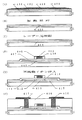
図3(A)と図3(B)に示すのは、非晶質珪素膜に対してレーザー光を照射して結晶性珪素膜を得た場合における得られた結晶性珪素膜の表面を写した写真である。
【0024】
図3(A)に示すのは、図1の104で示されるホモジナイザーを構成するシリンドリカルレンズの幅を5mmとし、その数を12個とした場合におけるアニール結果を示すものである。
【0025】
また、図3(B)に示すのは、図1の104で示されるホモジナイザーを構成するシリンドリカルレンズの幅を6.5 mmとし、その数を5個とした場合におけるアニール結果を示すものである。
【0026】
図2に図1の104で示されるホモジナイザーの拡大図を示す。ホモジナイザー201は、シリンドリカルレンズ202が複数集合して構成されている。また、aがシリンドリカルレンズの幅である。
【0027】
ここで重要となるのは、ホモジナイザーに入射したレーザー光の幅方向におけるシリンドリカルレンズの数を最低でも5個以上、好ましくは10個以上とすることである。上記レーザー光の幅方向は、レーザー光が最終的に線状となるその長手方向に一致または概略一致していることが重要である。
【0028】
また、図2に示されるシリンドリカルレンズ202の幅aを5mm以下とすることも重要である。この幅aの方向もレーザー光が最終的に線状となるその長手方向に一致または概略一致していることが必要である。なお、幅aの下限値は、0.1mm とすることが好ましい。
【0029】
図3に示す結果を得たアニールに用いた線状のレーザー光の長手方向の長さは、12cmである。なお、このレーザー光の長手方向における長さを変化させても、図3に示すようなアニール効果の違いは依然して表れてしまう。
【0030】
上記の条件を満たすことにより、図3(A)に示すように均一なアニールを施すことができる。
【0031】
なお、上記の条件を逸脱した場合、図3(B)に示すように、縦方向(レーザー光の長手方向に対応する)に伸びる縞模様が観察される。この縞模様は、線状レーザー光の長手方向における照射エネルギー密度のむらによるものである。
【0032】
なお、写真の水平方向に延長する縞模様(横縞)は、線状のレーザー光を走査して(ずらしながら)照射した場合に生じたむらであり、単なる照射条件の追い込み不足によるものである。
【0033】
図3(A)と(B)に示されるアニール効果の違いは、ホモジナイザー104の光学的なパラメータの設定が適切でなかったことの違いである。
【0034】
本明細書で開示する発明の一つは、
照射面における線状レーザー光の長さをx(mm)とし、
ホモジナイザーを構成するシリドリカルレンズの数をyとして、
xとyは、(43/600)x−(1/6)≦y≦(x/5)で示される数式を満足することを特徴とする。
【0035】
上記構成は、照射面における線状のレーザー光の長手方向の長さをシリンドリカルレンズの数で割った値が概略5mm〜15mmとなる条件を与えるものである。
【0036】
この数値範囲は、線状のレーザー光の長手方向における照射エネルギー密度の分布が均一なものとなる範囲として与えられる。
【0037】
本明細書で開示する他の発明の一つは、
線状のレーザー光を照射する装置であって、
線状のレーザー光の長手方向におけるエネルギー密度分布を制御するホモジナイザーを構成するシリンドリカルレンズの幅を0.1 mm〜5mmとすることを特徴とする。
【0038】
他の発明の構成は、
線状のレーザー光を照射する装置であって、
線状のレーザー光の長手方向における長さ(mm)と線状のレーザー光の長手方向におけるエネルギー密度分布を制御するホモジナイザーを構成するシリンドリカルレンズの数との関係が(100,7),(700,50),(700,140),(100,20) で示される座標で画定される範囲内にあることを特徴とする。
【0039】
上記の座標を図7に示す。図7に示す関係は、最終的に照射される線状レーザーの長手方向におけるシリンドリカルレンズ1個あたりに対応する長さが概略5mm〜15mmの場合に高い均一性が得られることを示している。
【0040】
他の発明の構成は、線状のレーザー光を照射する装置であって、線状のレーザー光の長手方向における照射エネルギー密度を制御するホモジナイザーを有し、前記長手方向に対応する前記ホモジナイザーに入射するレーザー光の幅(mm)と前記ホモジナイザーを構成するシリンドリカルレンズの幅(mm)との関係が、(30,0.1),(80,0.1),(80,5),(50,5),(30,3)で画定される範囲内にあることを特徴とする。
【0041】
上記の座標を図8に示す。図8に示す関係は、ホモジナイザーに入射するレーザー光の線状レーザーの幅が30mm〜80mmであること、さらにそのレーザー光がホモジナイザーによって10分割以上されること、さらにシリンドリカルレンズの幅が0.1mm 〜5mmであること、を持たす条件を示している。
【0042】
ホモジナイザーは、図2の201に示すような形状を有しており、202で示されるシリンドリカルレンズが多数個集合して構成されている。
【0043】
線状のレーザー光の長手方向におけるエネルギー密度分布を制御するホモジナイザーは、例えば、図1に示す構成においては、103と104である。
【0044】
【実施例】
〔実施例1〕
本実施例は、図1に示す光学系に比較して、ホモジナイザーの数を半分とすることができる光学系に関する。
【0045】
図6に本実施例の光学系を示す。図6に示す光学系においては、発振器601から発振されたレーザー光は、レンズ602とレンズ603で構成される光学系によって、所定のビーム形状と所定のエネルギー密度の分布を有したレーザー光に成形される。
【0046】
そしてこのレーザー光は2つのホモジナイザー604と605によってそのビーム内エネルギー密度の分布が補正される。
【0047】
ホモジナイザー604は、最終的に線状に成形されるレーザービームの幅方向におけるビーム内エネルギー密度の補正を行なう役割を担っている。しかし、線状レーザービームの幅方向の寸法は、数mm程度であるので、このホモジナイザー604が果たす役割はそう大きなものではない。
【0048】
ホモジナイザー605は、最終的に線状に成形されるレーザービームの長手方向におけるビーム内エネルギー密度の補正を行なう役割を担っている。レーザービームは、長手方向に10cm以上も引き延ばされるので、このホモジナイザー605の光学パラメータの設定は慎重に行なう必要がある。
【0049】
606と607と609とは、レーザービームを線状に成形する役割を担っている。また608はミラーである。
【0050】
図6に示す構成においては、線状に成形されたレーザービームの長手方向における照射エネルギー密度のむらの発生を左右する主なパラメーターがホモジナイザー605のおけるもののみであることが特徴である。従って、線状レーザーの長手方向におけるアニールむらの発生を抑えるための光学パラメータの設定が容易であるという特徴がある。
【0051】
本実施例に示す構成においては、ホモジナイザー605を12個のシリンドリカルレンズ(幅5mm)で構成し、入射するレーザー光をおよそ10分割するものとしている。
【0052】
即ち、ホモジナイザーは、内側の10個のシリンドリカルレンズが主に利用されるように、レーザー光に対して多少の余裕をもって配置されている。
【0053】
本実施例においては、最終的に照射される線状のレーザー光の長手方向の長さは12cmである。
【0054】
本実施例に示す構成を採用すると、線状レーザー光の長手方向におけるエネルギー密度のムラを是正することができ、均一なアニールを半導体材料に対して与えることができる。
【0055】
〔実施例2〕
本実施例は、本明細書に開示する発明を利用して、薄膜トランジスタを作製する場合の例を示す。図4に本実施例に示す薄膜トランジスタの作製工程を示す。
【0056】
まず、401で示されるガラス基板上に下地膜として酸化珪素膜または酸化窒化珪素膜402をスパッタ法またはプラズマCVD法により、3000Åの厚さに成膜する。
【0057】
次に非晶質珪素膜403をプラズマCVD法または減圧熱CVD法で500Åの厚さに成膜する。膜質の緻密さや後に得られる結晶性珪素膜の結晶性を考えた場合、この非晶質珪素膜403の成膜手段として減圧熱CVD法を用いることが好ましい。
【0058】
また、レーザー光の照射によるアニール効果を高めるために、非晶質珪素膜403の膜厚は、1000Å以下、好ましくは500Å以下とすることが重要となる。なお非晶質珪素膜403の膜厚の下限は、200Å程度である。
【0059】
次に珪素の結晶化を助長する金属元素の導入を行なう。ここでは、この珪素の結晶化を助長する金属元素としてNiを利用する。Ni以外には、Fe、Co、Cu、Pd、Pt、Au等を利用することができる。
【0060】
ここでは、ニッケル酢酸塩溶液を用いてNi元素の導入を行なう。具体的には、まず所定のNi濃度(ここでは10ppm(重量換算))に調整したニッケル酢酸塩溶液を非晶質珪素膜403の表面に滴下する。こうして状態でニッケル酢酸塩溶液の水膜404が形成される。(図4(A))
【0061】
次に図示しないスピンコーターを用いてスピンドライを行い、余分な溶液を吹き飛ばす。さらに550℃、4時間の加熱処理を行なうことにより、結晶性珪素膜405を得る。(図4(B))
【0062】
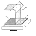
結晶性珪素膜405を得たら、次にレーザー光の照射を行う。このレーザー光の照射を行うことで、さらにその結晶性が向上される。ここでは、線状にビーム加工されたKrFエキシマレーザーを走査しながら照射することにより、このレーザーアニールを行なう。
【0063】
このレーザーアニールの様子を図5に示す。レーザービームは、図1に示すような光学系を利用して502で示されるような線状の形状を有したものとする。
【0064】
この線状のレーザー光は、基板を図5の矢印の方向に移動させながら照射することで、線状の長手方向に直角な方向に走査して照射される。
【0065】
図5において、501がレーザー光の照射が行なわれる以前の領域であり、503がレーザー光の照射がすでに行なわれた領域である。
【0066】
ここで図2に示すようなホモジナイザーをaで示される幅を5mm以下(下限は0.1 mm程度とするのが好ましい)とし、さらに入射するレーザー光を10以上に分割するように光学パラメータを設定する。
【0067】
このようにすることで、線状のレーザービーム502の長手方向における照射エネルギー密度のむらが是正され、その方向におけるアニール効果を均一なものとすることができる。
【0068】
図9にホモジナイザーによる分割を9分割とした場合の矩形波レーザービームのプロファイル例を示す。この矩形波レーザービームのプロファイルは、線状レーザーの幅方向のビームプロファイルに対応する。
【0069】
図10にホモジナイザーによる分割を18分割とした場合の矩形波レーザービームのプロファイル例を示す。図9と図10を比較すれば明らかなように、分割数を多くすることにより、レーザービームの均一性を向上させることができる。
【0070】
なお、図10の場合の方がエネルギー密度が高くなっているのは、光学系を変更したことによる損失の違いを反映したものと考えられる。
【0071】
図4(C)に示すレーザーアニールを施すことによって、さらに結晶性の高められた結晶性珪素膜406を得る。
【0072】
次にパターニングを行い、薄膜トランジスタの活性層となる領域406を形成する。(図4(D))
【0073】
さらに活性層406を覆ってゲイト絶縁膜として機能する酸化珪素膜407を形成する。ここではゲイト絶縁膜407として、プラズマCVD法によって1000Å厚の酸化珪素膜を成膜する。
【0074】
次にゲイト電極を構成するための図示しないアルミニウム膜を5000Åの厚さに成膜する。このアルミニウム膜中には、後の工程にヒロックやウィスカーが発生してしまうことを抑制するためにスカンジウムを0.1 重量%含有させる。
【0075】
ヒロックやウィスカーは、アルミニウムの異常成長によって形成される針状あるいは刺状の突起物のことである。
【0076】
次に図示しないレジストマスクを配置し、このマスクを用いて図示しないアルミニウム膜をパターニングする。こうして、ゲイト電極408を構成するためのパターンを形成する。ゲイト電極を構成するためのパターンを形成したら、先のレジストマスクを配置した状態で陽極酸化膜の形成を行なう。
【0077】
ここでは、電解溶液として3%のショウ酸を含んだ水溶液を用いる。即ち、この水溶液中において、図示しないアルミニウム膜のパターンを陽極とし、白金を陰極として電極間に電流を流し、アルミニウム膜のパターンの露呈した表面に陽極酸化膜を形成する。
【0078】
この工程で形成される陽極酸化膜409は、多孔質状(ポーラス状)を有している。またここでは、図示しないレジストマスクが存在するためにパターンの側面に409で示されるようにこの多孔質状の陽極酸化膜が形成される。
【0079】
この多孔質状の陽極酸化膜の膜厚は、3000Åとする。この多孔質状の陽極酸化膜の膜厚でもってオフセットゲイト領域を形成することができる。
【0080】
次に図示しないレジストマスクを除去し、再度の陽極酸化を行なう。この工程においては、3%の酒石酸を含んだエチレングリコール溶液をアンモニアで中和したものを電解溶液として用いる。
【0081】
この工程で形成される陽極酸化膜は、緻密な膜質を有している。この工程においては印加電圧を調整することにより、500Å厚の緻密な陽極酸化膜410を形成する。
【0082】
ここでは、多孔質状の陽極酸化膜409の内部に電界溶液が侵入するので、410で示されるようにゲイト電極408に接する状態で緻密な膜質を有する陽極酸化膜が形成される。
【0083】
この緻密な膜質を有する陽極酸化膜410の膜厚を厚くすると、その厚さの分で後にオフセットゲイト領域を形成を行うことができる。しかし、ここではその厚さが薄いので、オフセットゲイト領域の形成に際する寄与は無視する。
【0084】
こうして、図4(D)に示す状態を得る。図4(D)に示す状態を得たら、ソース及びドレイン領域を構成するための不純物イオンの注入を行なう。ここでは、Nチャネル型の薄膜トランジスタを作製するためにP(リン)イオンの注入を行なう。
【0085】
図4(D)の状態で不純物イオンの注入を行なうと、411と415の領域に不純物イオンが注入される。また412と414の領域は不純物イオンの注入がされず、かつゲイト電極408からの電界効果を受けない領域となる。この412と414の領域がオフセットゲイト領域として機能する。
【0086】
そして413で示される領域がチャネル形成領域となる。このようにして、図4(E)に示す状態を得る。
【0087】
上記不純物イオンの注入が終了したら、レーザー光の照射を行い、不純物イオンの注入された領域の活性化を行なう。このレーザー光の照射も図1にその光学系を有するレーザー照射装置を用い、図5にその照射状態を示す方法で行なう。
【0088】
図4(E)に示す状態を得たら、層間絶縁膜として、酸化珪素膜や窒化珪素膜、また酸化窒化珪素膜、さらにはそれらの積層膜でもって層間絶縁膜416を形成する。
【0089】
そしてコンタクトホールの形成を行い、ソース電極417とドレイン電極418の形成を行なう。このようにして図4(F)に示す薄膜トランジスタを完成させる。
【0090】
〔実施例3〕
本実施例は、実施例2に示す構成において、XeClレーザー(波長308nm)を用いる場合の例である。
【0091】
珪素膜に対するアニール効果を考えた場合、波長の短いKrFエキシマレーザー(波長248nm)を用いることがより好ましい。これは、波長の短いレーザー光の方がより珪素膜に吸収されやすいからである。
【0092】
しかし、装置のメンテナンスや発振器の安定性を考慮した場合、KrFエキシマレーザーより波長の長いXeClエキシマレーザーを用いる方が好ましい。
【0093】
これは、波長が長い分(振動数は小さくなる)、その光子エネルギー(hν)が小さく、光学系や発振器に与える負担が低くなるからである。
【0094】
〔実施例4〕
図7に示すところが意味するのは、ホモジナイザーを構成するシリンドリカルレンズ一に対応する最終的な照射面におけるレーザー光の長さを概略5mm〜15mmにすることが、照射密度の均一性から見て好ましいということである。
【0095】
即ち、照射面における線状のレーザー光の長手方向の長さをシリンドリカルレンズの数で割った値が概略5mm〜15mmとなることが好ましいということである。
【0096】
上記の条件を満足するならば、照射面における線状のレーザー光の長さが700mm以上でもよいことになる。
【0097】
本実施例は、図7で規定される条件に限定されず、図11に示すように、照射面における線状レーザー光の長手方向の長さの上限を限定しない例に関する。
【0098】
この場合、照射面における線状レーザー光の長さをx(mm)、シリドリカルレンズの数をyとして、(43/600)x−(1/6)≦y≦(x/5)で示される数式を満足するxとyの組み合わせを選択することができる。なお、xは5以上、好ましくは10以上とする。上記数式は、図7に示される線状レーザーの長さとシリンドリカルレンズの数との関係から得られる。
【0099】
例えば、照射面における線状レーザー光の長さをが1000mmであれば、シリンドリカルレンズの数は、72〜200の範囲から選択すればよい。
【0100】
逆にシリンドリカルレンズの数が100個のホモジナイザーを利用するのであれば、照射面における線状レーザー光の長さを500mm〜1398mmの範囲から選択すればよい。即ち、照射面における線状レーザー光の長さが500mm〜1398mmの範囲に収まるように光学系を設計すればよい。
【0101】
なお、上述する数式の範囲から照射面における線状レーザー光の長さと、シリドリカルレンズの数との組を選択した場合において、シリンドリカルレンズの幅を0.1mm 〜5mmから選択することが重要である。
【0102】
【発明の効果】
本明細書で開示する発明を利用することにより、半導体装置の作製に利用されるレーザープロセスにおいて、大面積に渡り均一なアニールを施すことができる技術を提供することができる。
【図面の簡単な説明】
【図1】 レーザー照射装置の光学系の概略を示す図。
【図2】 ホモジナイザーの形状を示す概略図。
【図3】 薄膜を示す写真。
【図4】 薄膜トランジスタの作製工程を示す図。
【図5】 線状のレーザー光を照射する状態を示す図。
【図6】 レーザー照射装置の光学系の概略を示す図。
【図7】 シリンドリカルレンズの数と照射面における線状レーザーの長手方向の長さとの関係を示す図。
【図8】 シリンドリカルレンズの幅とホモジナイザーに入射するレーザー光の幅の関係を示す図。
【図9】 9分割されたホモジナイザーを通した矩形レーザー波のビームプロファイルを示す図。
【図10】18分割されたホモジナイザーを通した矩形レーザー波のビームプ
ロファイルを示す図。
【図11】シリンドリカルレンズの数と照射面における線状レーザーの長手方向の長さとの関係を示す図。
【符号の説明】
101 レーザー発振器
102 ホモジナイザー
103 ホモジナイザー
104 ホモジナイザー
105 ホモジナイザー
106 レンズ
107 レンズ
108 レンズ
109 ミラー
110 レンズ
111 被照射面
201 ホモジナイザー
202 シリンドリカルレンズ
601 レーザー発振器
602 レンズ
603 レンズ
604 ホモジナイザー
605 ホモジナイザー
606 レンズ
607 レンズ
108 ミラー
609 レンズ[0001]
[Industrial application fields]
The invention disclosed in this specification relates to an apparatus for annealing a semiconductor material by laser light irradiation.
[0002]
[Prior art]
Conventionally, a technique of crystallization by irradiating laser light to an amorphous silicon film is known. In addition, a technique for irradiating a laser beam to recover the crystallinity of a silicon film damaged by implantation of impurity ions or to activate the implanted impurity ions is known.
[0003]
As a typical example of the latter technique, an example of annealing the source and drain regions of a thin film transistor can be given. In this method, after the impurity ions represented by phosphorus or boron are implanted into the region, the region is annealed by laser light irradiation.
[0004]
Such a process by laser light irradiation (generally called a laser process) has a feature that there is almost no thermal damage to the substrate.
[0005]
The feature that there is no problem of thermal damage to the substrate is important when manufacturing an active matrix liquid crystal display device whose use range has been expanded in recent years.
[0006]
In an active matrix liquid crystal display device, it is desired to use a glass substrate as a substrate because of cost problems and a demand for a large area.
[0007]
However, the glass substrate cannot withstand heat treatment at a high temperature of 600 ° C. or higher, or 700 ° C. or higher. As a technique for avoiding this problem, a technique for performing crystallization of the above-described silicon film and annealing after impurity ions by laser light irradiation is useful.
[0008]
In the method using laser light irradiation, even when a glass substrate is used as the substrate, there is almost no thermal damage to the glass substrate. Accordingly, a thin film transistor using a crystalline silicon film can be manufactured using a glass substrate.
[0009]
However, the laser process has a problem that the processing efficiency for a large area is low because the beam area of the laser beam is small. In addition, there is a method of processing a large area by scanning with laser light, but in this case, there are problems such as low in-plane uniformity of processing effects.
[0010]
[Problems to be solved by the invention]
An object of the invention disclosed in this specification is to provide a technique capable of performing uniform annealing over a large area in a laser process used for manufacturing a semiconductor device.
[0011]
[Means for Solving the Problems]
An example of a laser irradiation apparatus using the invention disclosed in this specification is shown in FIG. In FIG. 1,
[0012]
For example, a KrF excimer laser oscillates laser light by high frequency discharge using Kr and F as source gases.
[0013]
[0014]
This optical correction in the vertical direction contributes to the uniformization of the energy density in the width direction of the laser beam finally formed into a linear shape.
[0015]
The
[0016]
This optical correction in the horizontal direction contributes to the uniformization of the energy density in the longitudinal direction of the line of the laser beam finally formed into a linear shape.
[0017]
A
[0018]
[0019]
The irradiated
[0020]
What is important here is the setting of the optical parameters of the
[0021]
In general, if the optical parameters of the
[0022]
The invention disclosed in this specification is characterized by correcting the unevenness of the irradiation energy density generated in the longitudinal direction of the linear beam by optimizing the optical parameters of the
[0023]
FIGS. 3A and 3B show the surface of the obtained crystalline silicon film when the amorphous silicon film is irradiated with laser light to obtain the crystalline silicon film. It is a photograph.
[0024]
FIG. 3A shows the annealing result when the width of the cylindrical lens constituting the homogenizer indicated by 104 in FIG. 1 is 5 mm and the number thereof is twelve.
[0025]
FIG. 3B shows the annealing results when the width of the cylindrical lens constituting the homogenizer indicated by 104 in FIG. 1 is 6.5 mm and the number thereof is five.
[0026]
FIG. 2 shows an enlarged view of the homogenizer indicated by 104 in FIG. The
[0027]
Here An important is ho motor Jinaiza the number of cylindrical lenses in the width direction of the
[0028]
It is also important that the width a of the
[0029]
The length in the longitudinal direction of the linear laser beam used for annealing with the results shown in FIG. 3 is 12 cm. Even if the length of the laser beam in the longitudinal direction is changed, the difference in annealing effect as shown in FIG. 3 still appears.
[0030]
By satisfying the above conditions, uniform annealing can be performed as shown in FIG.
[0031]
In addition, when it deviates from said conditions, as shown to FIG. 3 (B), the striped pattern extended in the vertical direction (corresponding to the longitudinal direction of a laser beam) is observed. This striped pattern is due to unevenness of the irradiation energy density in the longitudinal direction of the linear laser beam.
[0032]
The striped pattern (horizontal stripe) extending in the horizontal direction of the photograph is unevenness generated when the linear laser beam is irradiated while being scanned (shifted), and is simply due to insufficient follow-up of irradiation conditions.
[0033]
The difference in the annealing effect shown in FIGS. 3A and 3B is that the optical parameter setting of the
[0034]
One of the inventions disclosed in this specification is:
The length of the linear laser beam on the irradiated surface is x (mm),
Let y be the number of cylindrical lenses constituting the homogenizer.
x and y satisfy the equation represented by (43/600) x− (1/6) ≦ y ≦ (x / 5).
[0035]
The said structure gives the conditions from which the value which divided the length of the linear direction of the linear laser beam in an irradiation surface by the number of cylindrical lenses will be about 5 mm-15 mm.
[0036]
This numerical range is given as a range in which the distribution of the irradiation energy density in the longitudinal direction of the linear laser light is uniform.
[0037]
One of the other inventions disclosed in this specification is:
An apparatus for irradiating a linear laser beam,
The width of the cylindrical lens constituting the homogenizer for controlling the energy density distribution in the longitudinal direction of the linear laser light is 0.1 mm to 5 mm.
[0038]
Other aspects of the invention are:
An apparatus for irradiating a linear laser beam,
The relationship between the length (mm) of the linear laser beam in the longitudinal direction and the number of cylindrical lenses constituting the homogenizer that controls the energy density distribution in the longitudinal direction of the linear laser beam is (100,7), (700 , 50), (700, 140), (100, 20).
[0039]
The above coordinates are shown in FIG. The relationship shown in FIG. 7 indicates that high uniformity can be obtained when the length corresponding to one cylindrical lens in the longitudinal direction of the linear laser to be finally irradiated is approximately 5 mm to 15 mm.
[0040]
Another aspect of the invention is an apparatus for irradiating linear laser light, having a homogenizer that controls irradiation energy density in the longitudinal direction of the linear laser light, and entering the homogenizer corresponding to the longitudinal direction The relationship between the width (mm) of the laser beam to be produced and the width (mm) of the cylindrical lens constituting the homogenizer is (30, 0.1), (80 , 0.1), (80 , 5), (50 , 5) and (30, 3).
[0041]
The above coordinates are shown in FIG. The relationship shown in FIG. 8 is that the width of the linear laser beam incident on the homogenizer is 30 mm to 80 mm, the laser beam is further divided into 10 or more by the homogenizer, and the width of the cylindrical lens is 0.1 mm to The condition of having 5 mm is shown.
[0042]
The homogenizer has a shape as indicated by 201 in FIG. 2, and is configured by assembling a large number of cylindrical lenses indicated by 202.
[0043]
The homogenizers that control the energy density distribution in the longitudinal direction of the linear laser beam are, for example, 103 and 104 in the configuration shown in FIG.
[0044]
【Example】
[Example 1]
This embodiment relates to an optical system that can halve the number of homogenizers as compared to the optical system shown in FIG.
[0045]
FIG. 6 shows the optical system of this embodiment. In the optical system shown in FIG. 6, laser light oscillated from an
[0046]
The laser beam has its beam energy density distribution corrected by two
[0047]
The
[0048]
The
[0049]
[0050]
The configuration shown in FIG. 6 is characterized in that the main parameter that affects the generation of unevenness of the irradiation energy density in the longitudinal direction of the linearly shaped laser beam is only that which can be used in the
[0051]
In the configuration shown in the present embodiment, the
[0052]
That is, the homogenizer is arranged with a slight margin with respect to the laser beam so that the inner 10 cylindrical lenses are mainly used.
[0053]
In the present embodiment, the length of the linear laser beam finally irradiated is 12 cm in the longitudinal direction.
[0054]
When the configuration shown in this embodiment is adopted, unevenness in energy density in the longitudinal direction of the linear laser beam can be corrected, and uniform annealing can be given to the semiconductor material.
[0055]
[Example 2]
This embodiment shows an example of manufacturing a thin film transistor by using the invention disclosed in this specification. FIG. 4 shows a manufacturing process of the thin film transistor described in this embodiment.
[0056]
First, a silicon oxide film or a silicon oxynitride film 402 is formed as a base film on a glass substrate indicated by 401 to a thickness of 3000 mm by a sputtering method or a plasma CVD method.
[0057]
Next, an amorphous silicon film 403 is formed to a thickness of 500 mm by plasma CVD or low pressure thermal CVD. In consideration of the denseness of the film quality and the crystallinity of the crystalline silicon film obtained later, it is preferable to use a low pressure thermal CVD method as a means for forming the amorphous silicon film 403.
[0058]
Further, in order to enhance the annealing effect by laser light irradiation, it is important that the thickness of the amorphous silicon film 403 is 1000 mm or less, preferably 500 mm or less. Note that the lower limit of the thickness of the amorphous silicon film 403 is about 200 mm.
[0059]
Next, a metal element that promotes crystallization of silicon is introduced. Here, Ni is used as a metal element for promoting the crystallization of silicon. In addition to Ni, Fe, Co, Cu, Pd, Pt, Au, etc. can be used.
[0060]
Here, Ni element is introduced using a nickel acetate solution. Specifically, first, a nickel acetate solution adjusted to a predetermined Ni concentration (here, 10 ppm (weight conversion)) is dropped onto the surface of the amorphous silicon film 403. In this state, a nickel acetate
[0061]
Next, spin drying is performed using a spin coater (not shown), and excess solution is blown off. Further, a
[0062]
After the
[0063]
The state of this laser annealing is shown in FIG. The laser beam is assumed to have a linear shape as indicated by 502 using an optical system as shown in FIG.
[0064]
This linear laser beam is irradiated while being scanned in a direction perpendicular to the linear longitudinal direction by irradiating the substrate while moving the substrate in the direction of the arrow in FIG.
[0065]
In FIG. 5,
[0066]
Here, in the homogenizer as shown in FIG. 2, the width indicated by a is set to 5 mm or less (the lower limit is preferably about 0.1 mm), and the optical parameters are set so that the incident laser light is divided into 10 or more. .
[0067]
By doing so, the unevenness of the irradiation energy density in the longitudinal direction of the
[0068]
FIG. 9 shows a profile example of a rectangular wave laser beam when the division by the homogenizer is nine divisions. The profile of this rectangular wave laser beam corresponds to the beam profile in the width direction of the linear laser.
[0069]
FIG. 10 shows an example of a profile of a rectangular wave laser beam when dividing by the homogenizer is 18 divisions. As is clear from comparison between FIG. 9 and FIG. 10, the uniformity of the laser beam can be improved by increasing the number of divisions.
[0070]
Note that the energy density in the case of FIG. 10 is considered to reflect the difference in loss due to the change of the optical system.
[0071]
By performing laser annealing shown in FIG. 4C, a
[0072]
Next, patterning is performed to form a
[0073]
Further, a
[0074]
Next, an aluminum film (not shown) for forming the gate electrode is formed to a thickness of 5000 mm. This aluminum film contains scandium in an amount of 0.1% by weight in order to suppress the occurrence of hillocks and whiskers in the subsequent process.
[0075]
Hillocks and whiskers are needle-like or stab-like projections formed by abnormal growth of aluminum.
[0076]
Next, a resist mask (not shown) is arranged, and an aluminum film (not shown) is patterned using this mask. Thus, a pattern for forming the gate electrode 408 is formed. After the pattern for forming the gate electrode is formed, the anodic oxide film is formed in the state where the previous resist mask is arranged.
[0077]
Here, an aqueous solution containing 3% oxalic acid is used as the electrolytic solution. That is, in this aqueous solution, an aluminum film pattern (not shown) is used as an anode, platinum is used as a cathode, an electric current is passed between the electrodes, and an anodized film is formed on the exposed surface of the aluminum film pattern.
[0078]
The
[0079]
The thickness of the porous anodic oxide film is 3000 mm. The offset gate region can be formed with the thickness of the porous anodic oxide film.
[0080]
Next, the resist mask (not shown) is removed and anodic oxidation is performed again. In this step, an electrolytic solution obtained by neutralizing an ethylene glycol solution containing 3% tartaric acid with ammonia is used.
[0081]
The anodized film formed in this process has a dense film quality. In this step, a dense anodic oxide film 410 having a thickness of 500 mm is formed by adjusting the applied voltage.
[0082]
Here, since the electric field solution penetrates into the porous
[0083]
When the thickness of the anodic oxide film 410 having a dense film quality is increased, an offset gate region can be formed later by the thickness. However, since the thickness is thin here, the contribution in forming the offset gate region is ignored.
[0084]
In this way, the state shown in FIG. After obtaining the state shown in FIG. 4D, impurity ions are implanted to form the source and drain regions. Here, P (phosphorus) ions are implanted in order to manufacture an N-channel thin film transistor.
[0085]
When impurity ions are implanted in the state of FIG. 4D, impurity ions are implanted into the regions 411 and 415. Further, the regions 412 and 414 are regions which are not implanted with impurity ions and are not subjected to the field effect from the gate electrode 408. The areas 412 and 414 function as offset gate areas.
[0086]
A region indicated by 413 is a channel formation region. In this way, the state shown in FIG.
[0087]
When the impurity ion implantation is completed, laser light irradiation is performed to activate the region into which the impurity ions are implanted. This laser light irradiation is also performed by the method shown in FIG. 5 using the laser irradiation apparatus having the optical system shown in FIG.
[0088]
After obtaining the state shown in FIG. 4E, an interlayer insulating film 416 is formed using a silicon oxide film, a silicon nitride film, a silicon oxynitride film, or a stacked film thereof as an interlayer insulating film.
[0089]
Then, contact holes are formed, and a source electrode 417 and a drain electrode 418 are formed. In this manner, the thin film transistor shown in FIG. 4F is completed.
[0090]
Example 3
The present embodiment is an example in the case where a XeCl laser (wavelength 308 nm) is used in the configuration shown in the second embodiment.
[0091]
In view of the annealing effect on the silicon film, it is more preferable to use a KrF excimer laser (wavelength 248 nm) having a short wavelength. This is because laser light having a shorter wavelength is more easily absorbed by the silicon film.
[0092]
However, considering the maintenance of the apparatus and the stability of the oscillator, it is preferable to use a XeCl excimer laser having a longer wavelength than the KrF excimer laser.
[0093]
This is because the photon energy (hν) is small because the wavelength is long (the frequency is small), and the burden on the optical system and the oscillator is low.
[0094]
Example 4
What is shown in FIG. 7 means that the length of the laser beam on the final irradiation surface corresponding to the cylindrical lens constituting the homogenizer is preferably about 5 mm to 15 mm in view of uniformity of irradiation density. That's what it means.
[0095]
That is, it is preferable that the value obtained by dividing the length of the linear laser beam in the irradiation surface in the longitudinal direction by the number of cylindrical lenses is approximately 5 mm to 15 mm.
[0096]
If the above conditions are satisfied, the length of the linear laser beam on the irradiated surface may be 700 mm or more.
[0097]
The present embodiment is not limited to the conditions defined in FIG. 7, but relates to an example in which the upper limit of the length of the linear laser beam on the irradiation surface is not limited as shown in FIG.
[0098]
In this case, assuming that the length of the linear laser beam on the irradiated surface is x (mm) and the number of cylindrical lenses is y, (43/600) x− (1/6) ≦ y ≦ (x / 5) A combination of x and y that satisfies the equation shown can be selected. Note that x is 5 or more, preferably 10 or more. The above formula is obtained from the relationship between the length of the linear laser shown in FIG. 7 and the number of cylindrical lenses.
[0099]
For example, if the length of the linear laser beam on the irradiation surface is 1000 mm, the number of cylindrical lenses may be selected from a range of 72 to 200.
[0100]
Conversely, if a homogenizer with 100 cylindrical lenses is used, the length of the linear laser beam on the irradiated surface may be selected from a range of 500 mm to 1398 mm. That is, the optical system may be designed so that the length of the linear laser beam on the irradiation surface is within the range of 500 mm to 1398 mm.
[0101]
In addition, when the combination of the length of the linear laser beam on the irradiation surface and the number of cylindrical lenses is selected from the range of the above-described mathematical formula, it is important to select the width of the cylindrical lens from 0.1 mm to 5 mm. is there.
[0102]
【The invention's effect】
By utilizing the invention disclosed in this specification, a technique capable of performing uniform annealing over a large area in a laser process used for manufacturing a semiconductor device can be provided.
[Brief description of the drawings]
FIG. 1 is a diagram showing an outline of an optical system of a laser irradiation apparatus.
FIG. 2 is a schematic diagram showing the shape of a homogenizer.
FIG. 3 is a photograph showing a thin film.
4A and 4B illustrate a manufacturing process of a thin film transistor.
FIG. 5 is a diagram showing a state in which linear laser light is irradiated.
FIG. 6 is a diagram showing an outline of an optical system of a laser irradiation apparatus.
FIG. 7 is a diagram showing the relationship between the number of cylindrical lenses and the length in the longitudinal direction of the linear laser on the irradiated surface.
FIG. 8 is a diagram showing the relationship between the width of a cylindrical lens and the width of laser light incident on a homogenizer.
FIG. 9 is a diagram showing a beam profile of a rectangular laser wave that has passed through a homogenizer divided into nine parts.
FIG. 10 is a diagram showing a beam profile of a rectangular laser wave that has passed through a homogenizer divided into 18 parts.
FIG. 11 is a diagram showing the relationship between the number of cylindrical lenses and the length of the linear laser on the irradiation surface in the longitudinal direction.
[Explanation of symbols]
DESCRIPTION OF
Claims (22)
前記レーザー光の所定の方向におけるエネルギー密度分布を制御する第1のホモジナイザーおよび第2のホモジナイザーと、
前記第1のホモジナイザーおよび前記第2のホモジナイザーを通った前記レーザー光を照射面において線状に成形する手段とを有し、
前記第1のホモジナイザーと前記第2のホモジナイザーは、それぞれ複数のシリンドリカルレンズを有し、
前記所定の方向は、前記線状に成形されたレーザー光の長手方向であり、
前記第1のホモジナイザーおよび前記第2のホモジナイザーのそれぞれに入射する前記レーザー光の幅(mm)を横軸とし、前記第1のホモジナイザーおよび前記第2のホモジナイザーのそれぞれが有する前記シリンドリカルレンズの幅(mm)を縦軸とすると、
前記横軸と前記縦軸の関係が(30,0.1)、(80,0.1)、(80,5)、(50,5)、(30,3)で示される座標で画定される領域以内にあり、
前記照射面における前記線状に成形されたレーザー光の長手方向における長さを、前記第1のホモジナイザーおよび前記第2のホモジナイザーのそれぞれが有する前記シリンドリカルレンズの数で割った値が、5mm〜15mmであることを特徴とするレーザー照射装置。Means for oscillating laser light;
A first homogenizer and a second homogenizer for controlling an energy density distribution in a predetermined direction of the laser beam;
And means for forming linearly on the irradiation surface of the laser light through the first homogenizer and the second homogenizer over,
The first homogenizer and the second homogenizer each have a plurality of cylindrical lenses,
The predetermined direction is a longitudinal direction of the laser beam formed into the linear shape,
The horizontal axis of the width (mm) of the laser light incident on each of the first homogenizer and the second homogenizer, and the width of the cylindrical lens included in each of the first homogenizer and the second homogenizer ( mm) is the vertical axis,
The relationship between the horizontal axis and the vertical axis is defined by the coordinates indicated by (30,0.1), (80,0.1), (80,5), (50,5), (30,3). Within the area
A value obtained by dividing the length in the longitudinal direction of the linearly shaped laser beam on the irradiation surface by the number of the cylindrical lenses of each of the first homogenizer and the second homogenizer is 5 mm to 15 mm. The laser irradiation apparatus characterized by being.
前記レーザー光は、前記第1のホモジナイザーおよび前記第2のホモジナイザーによって、それぞれ10分割以上されることを特徴とするレーザー照射装置。In claim 1,
The laser beam is divided into 10 or more by the first homogenizer and the second homogenizer, respectively.
前記第1のホモジナイザーおよび前記第2のホモジナイザーは、それぞれ10個以上の前記シリンドリカルレンズを有することを特徴とするレーザー照射装置。In claim 1,
Each of the first homogenizer and the second homogenizer includes 10 or more cylindrical lenses.
前記レーザー光の第1の方向におけるエネルギー密度分布を制御する第1のホモジナイザーおよび第2のホモジナイザーと、
前記レーザー光の第2の方向におけるエネルギー密度分布を制御する第3のホモジナイザーおよび第4のホモジナイザーと、
前記第1乃至第4のホモジナイザーを通った前記レーザー光を、照射面において線状に成形する手段とを有し、
前記第1乃至第4のホモジナイザーは、それぞれ複数のシリンドリカルレンズを有し、
前記第1の方向は、前記線状に成形されたレーザー光の長手方向であり、
前記第2の方向は、前記線状に成形されたレーザー光の幅方向であり、
前記第1のホモジナイザーおよび前記第2のホモジナイザーのそれぞれに入射する前記レーザー光の幅(mm)を横軸とし、前記第1のホモジナイザーおよび前記第2のホモジナイザーのそれぞれが有する前記シリンドリカルレンズの幅(mm)を縦軸とすると、
前記横軸と前記縦軸の関係が(30,0.1)、(80,0.1)、(80,5)、(50,5)、(30,3)で示される座標で画定される領域以内にあり、
前記照射面における前記線状に成形されたレーザー光の長手方向における長さを、前記第1のホモジナイザーおよび前記第2のホモジナイザーのそれぞれが有する前記シリンドリカルレンズの数で割った値が、5mm〜15mmであることを特徴とするレーザー照射装置。Means for oscillating laser light;
A first homogenizer and a second homogenizer for controlling an energy density distribution in a first direction of the laser beam;
A third homogenizer and a fourth homogenizer for controlling an energy density distribution in the second direction of the laser beam;
Said first through said laser beam passing through the fourth homogenizer over, and means for forming linearly on the irradiation surface,
The first to fourth homogenizers each have a plurality of cylindrical lenses,
The first direction is a longitudinal direction of the laser beam formed into the linear shape,
The second direction is a width direction of the linearly shaped laser beam,
The width (mm) of the laser beam incident on each of the first homogenizer and the second homogenizer is a horizontal axis, and the width of the cylindrical lens ( mm) is the vertical axis,
The relationship between the horizontal axis and the vertical axis is defined by the coordinates indicated by (30,0.1), (80,0.1), (80,5), (50,5), (30,3). Within the area
A value obtained by dividing the length in the longitudinal direction of the linearly shaped laser beam on the irradiation surface by the number of the cylindrical lenses of each of the first homogenizer and the second homogenizer is 5 mm to 15 mm. The laser irradiation apparatus characterized by being.
前記レーザー光は、前記第1のホモジナイザーおよび前記第2のホモジナイザーによって、それぞれ10分割以上されることを特徴とするレーザー照射装置。In claim 4,
The laser beam is divided into 10 or more by the first homogenizer and the second homogenizer, respectively.
前記第1のホモジナイザーおよび前記第2のホモジナイザーは、それぞれ10個以上の前記シリンドリカルレンズを有することを特徴とするレーザー照射装置。In claim 4,
Each of the first homogenizer and the second homogenizer includes 10 or more cylindrical lenses.
前記照射面における前記線状に成形されたレーザー光の長手方向における長さをx(mm)とし、前記第1のホモジナイザーおよび前記第2のホモジナイザーのそれぞれが有する前記シリンドリカルレンズの数をyとすると、
前記xと前記yは、(43/600)x−(1/6)≦y≦(x/5)で示される数式を満足することを特徴とするレーザー照射装置。In any one of Claims 1 thru | or 6,
When the length in the longitudinal direction of the linearly shaped laser beam on the irradiation surface is x (mm), and the number of the cylindrical lenses included in each of the first homogenizer and the second homogenizer is y. ,
Said x and said y satisfy | fill the numerical formula shown by (43/600) x- (1/6) <= y <= (x / 5), The laser irradiation apparatus characterized by the above-mentioned.
前記第1のホモジナイザーおよび前記第2のホモジナイザーがそれぞれ有する前記シリンドリカルレンズの幅は、0.1mm〜5mmであることを特徴とするレーザー照射装置。In any one of Claims 1 thru | or 6,
The laser irradiation apparatus, wherein a width of the cylindrical lens included in each of the first homogenizer and the second homogenizer is 0.1 mm to 5 mm.
前記照射面における前記線状に成形されたレーザー光の長手方向における長さ(mm)を横軸とし、前記第1のホモジナイザーおよび前記第2のホモジナイザーがそれぞれ有する前記シリンドリカルレンズの数を縦軸とすると、
前記横軸と前記縦軸の関係が(100,7)、(700,50)、(700,140)、(100,20)で示される座標で画定される領域以内にあることを特徴とするレーザー照射装置。In any one of Claims 1 thru | or 6,
The length (mm) in the longitudinal direction of the linearly shaped laser beam on the irradiation surface is taken as the horizontal axis, and the number of the cylindrical lenses each of the first homogenizer and the second homogenizer is taken as the vertical axis. Then
The relationship between the horizontal axis and the vertical axis is within an area defined by coordinates indicated by (100, 7), (700, 50), (700, 140), and (100, 20). Laser irradiation device.
前記シリンドリカルレンズは、凸シリンドリカルレンズであることを特徴とするレーザー照射装置。In any one of Claims 1 thru | or 9,
The laser irradiation apparatus, wherein the cylindrical lens is a convex cylindrical lens.
前記レーザー光は、前記レーザー光の所定の方向におけるエネルギー密度分布を制御する第1のホモジナイザーおよび第2のホモジナイザーを通り、
前記第1のホモジナイザーおよび前記第2のホモジナイザーを通ったレーザー光を線状に成形し、
前記第1のホモジナイザーと前記第2のホモジナイザーは、それぞれ複数のシリンドリカルレンズを有し、
前記所定の方向は、前記線状に成形されたレーザー光の長手方向であり、
前記第1のホモジナイザーおよび前記第2のホモジナイザーのそれぞれに入射する前記レーザー光の幅(mm)を横軸とし、前記第1のホモジナイザーおよび前記第2のホモジナイザーのそれぞれが有する前記シリンドリカルレンズの幅(mm)を縦軸とすると、
前記横軸と前記縦軸の関係が(30,0.1)、(80,0.1)、(80,5)、(50,5)、(30,3)で示される座標で画定される領域以内にあり、
照射面における前記線状に成形されたレーザー光の長手方向における長さを、前記第1のホモジナイザーおよび前記第2のホモジナイザーのそれぞれが有する前記シリンドリカルレンズの数で割った値が、5mm〜15mmであることを特徴とするレーザー照射方法。Laser light is emitted from the laser oscillator,
The laser light passes through the first homogenizer and second homogenizer over controlling the energy density distribution in the predetermined direction of the laser beam,
Molding a laser beam through the first homogenizer and the second homogenizer over to linear,
The first homogenizer and the second homogenizer each have a plurality of cylindrical lenses,
The predetermined direction is a longitudinal direction of the laser beam formed into the linear shape,
The horizontal axis of the width (mm) of the laser light incident on each of the first homogenizer and the second homogenizer, and the width of the cylindrical lens included in each of the first homogenizer and the second homogenizer ( mm) is the vertical axis,
The relationship between the horizontal axis and the vertical axis is defined by the coordinates indicated by (30,0.1), (80,0.1), (80,5), (50,5), (30,3). Within the area
A value obtained by dividing the length in the longitudinal direction of the linearly shaped laser beam on the irradiation surface by the number of cylindrical lenses of each of the first homogenizer and the second homogenizer is 5 mm to 15 mm. A laser irradiation method characterized by being.
前記レーザー光は、前記第1のホモジナイザーおよび前記第2のホモジナイザーによってそれぞれ10分割以上されることを特徴とするレーザー照射方法。In claim 11,
The laser irradiation method according to claim 1, wherein the laser light is divided into 10 or more parts by the first homogenizer and the second homogenizer.
前記第1のホモジナイザーおよび前記第2のホモジナイザーは、それぞれ10個以上の前記シリンドリカルレンズを有することを特徴とするレーザー照射方法。In claim 11,
The first homogenizer and the second homogenizer each have 10 or more cylindrical lenses.
前記レーザー光は、前記レーザー光の第1の方向におけるエネルギー密度分布を制御する第1のホモジナイザーおよび第2のホモジナイザーを通り、
前記レーザー光は、前記レーザー光の第2の方向におけるエネルギー密度分布を制御する第3のホモジナイザーおよび第4のホモジナイザーを通り、
前記第1乃至第4のホモジナイザーを通ったレーザー光を線状に成形し、
前記第1乃至第4のホモジナイザーは、それぞれ複数のシリンドリカルレンズを有し、
前記第1の方向は、前記線状に成形されたレーザー光の長手方向であり、
前記第2の方向は、前記線状に成形されたレーザー光の幅方向であり、
前記第1のホモジナイザーおよび前記第2のホモジナイザーのそれぞれに入射する前記レーザー光の幅(mm)を横軸とし、前記第1のホモジナイザーおよび前記第2のホモジナイザーのそれぞれが有する前記シリンドリカルレンズの幅(mm)を縦軸とすると、
前記横軸と前記縦軸の関係が(30,0.1)、(80,0.1)、(80,5)、(50,5)、(30,3)で示される座標で画定される領域以内にあり、
照射面における前記線状に成形されたレーザー光の長手方向における長さを、前記第1のホモジナイザーおよび前記第2のホモジナイザーのそれぞれが有する前記シリンドリカルレンズの数で割った値が、5mm〜15mmであることを特徴とするレーザー照射方法。Laser light is emitted from the laser oscillator,
The laser light passes through the first homogenizer and second homogenizer over controlling the energy density distribution in the first direction of the laser beam,
The laser light passes through the third homogenizer and fourth homogenizer over controlling the energy density distribution in the second direction of the laser beam,
The first to laser light which has passed through the fourth homogenizer over molded linearly,
The first to fourth homogenizers each have a plurality of cylindrical lenses,
The first direction is a longitudinal direction of the laser beam formed into the linear shape,
The second direction is a width direction of the linearly shaped laser beam,
The width (mm) of the laser beam incident on each of the first homogenizer and the second homogenizer is a horizontal axis, and the width of the cylindrical lens ( mm) is the vertical axis,
The relationship between the horizontal axis and the vertical axis is defined by the coordinates indicated by (30,0.1), (80,0.1), (80,5), (50,5), (30,3). Within the area
A value obtained by dividing the length in the longitudinal direction of the linearly shaped laser beam on the irradiation surface by the number of the cylindrical lenses of each of the first homogenizer and the second homogenizer is 5 mm to 15 mm. A laser irradiation method characterized by being.
前記レーザー光は、前記第1のホモジナイザーおよび前記第2のホモジナイザーによってそれぞれ10分割以上されることを特徴とするレーザー照射方法。In claim 14,
The laser irradiation method according to claim 1, wherein the laser light is divided into 10 or more parts by the first homogenizer and the second homogenizer.
前記第1のホモジナイザー及び前記第2のホモジナイザーは、それぞれが10個以上の前記シリンドリカルレンズを有することを特徴とするレーザー照射方法。In claim 14,
Each of the first homogenizer and the second homogenizer includes 10 or more cylindrical lenses.
前記照射面における前記線状に成形されたレーザー光の長手方向における長さをx(mm)とし、前記第1のホモジナイザーおよび前記第2のホモジナイザーがそれぞれ有する前記シリンドリカルレンズの数をyとすると、
前記xと前記yは、(43/600)x−(1/6)≦y≦(x/5)で示される数式を満足することを特徴とするレーザー照射方法。In any one of Claims 11 thru | or 16,
When the length in the longitudinal direction of the linearly shaped laser beam on the irradiation surface is x (mm), and the number of the cylindrical lenses each of the first homogenizer and the second homogenizer is y,
Said x and said y satisfy | fill the numerical formula shown by (43/600) x- (1/6) <= y <= (x / 5), The laser irradiation method characterized by the above-mentioned.
前記第1のホモジナイザーおよび前記第2のホモジナイザーがそれぞれ有する前記シリンドリカルレンズの幅は、0.1mm〜5mmであることを特徴とするレーザー照射方法。In any one of Claims 11 thru | or 16,
The laser irradiation method, wherein a width of the cylindrical lens included in each of the first homogenizer and the second homogenizer is 0.1 mm to 5 mm.
前記照射面における前記線状に成形されたレーザー光の長手方向における長さ(mm)を横軸とし、前記第1のホモジナイザーおよび前記第2のホモジナイザーがそれぞれ有する前記シリンドリカルレンズの数を縦軸とすると、
前記横軸と前記縦軸の関係が(100,7)、(700,50)、(700,140)、(100,20)で示される座標で画定される領域以内にあることを特徴とするレーザー照射方法。In any one of Claims 11 thru | or 16,
The length (mm) in the longitudinal direction of the linearly shaped laser beam on the irradiation surface is taken as the horizontal axis, and the number of the cylindrical lenses each of the first homogenizer and the second homogenizer is taken as the vertical axis. Then
The relationship between the horizontal axis and the vertical axis is within an area defined by coordinates indicated by (100, 7), (700, 50), (700, 140), and (100, 20). Laser irradiation method.
前記シリンドリカルレンズは、凸シリンドリカルレンズであることを特徴とするレーザー照射方法。In any one of Claims 11 thru | or 19,
The laser irradiation method, wherein the cylindrical lens is a convex cylindrical lens.
前記レーザー光は、KrFエキシマレーザー光又はXeClエキシマレーザー光であることを特徴するレーザー照射方法。21. In any one of claims 11 to 20,
The laser irradiation method, wherein the laser light is KrF excimer laser light or XeCl excimer laser light.
前記レーザー光は、KrFエキシマレーザー光又はXeClエキシマレーザー光であることを特徴するレーザー照射装置。In any one of Claims 1 to 10,
The laser irradiation apparatus, wherein the laser light is KrF excimer laser light or XeCl excimer laser light.
Priority Applications (1)
| Application Number | Priority Date | Filing Date | Title |
|---|---|---|---|
| JP03446897A JP3917231B2 (en) | 1996-02-06 | 1997-02-03 | Laser irradiation apparatus and laser irradiation method |
Applications Claiming Priority (3)
| Application Number | Priority Date | Filing Date | Title |
|---|---|---|---|
| JP4430696 | 1996-02-06 | ||
| JP03446897A JP3917231B2 (en) | 1996-02-06 | 1997-02-03 | Laser irradiation apparatus and laser irradiation method |
| JP8-44306 | 1999-02-06 |
Related Child Applications (1)
| Application Number | Title | Priority Date | Filing Date |
|---|---|---|---|
| JP2005204124A Division JP4527018B2 (en) | 1996-02-06 | 2005-07-13 | Method for manufacturing semiconductor device |
Publications (2)
| Publication Number | Publication Date |
|---|---|
| JPH09275081A JPH09275081A (en) | 1997-10-21 |
| JP3917231B2 true JP3917231B2 (en) | 2007-05-23 |
Family
ID=12687817
Family Applications (3)
| Application Number | Title | Priority Date | Filing Date |
|---|---|---|---|
| JP03446897A Expired - Fee Related JP3917231B2 (en) | 1996-02-06 | 1997-02-03 | Laser irradiation apparatus and laser irradiation method |
| JP2005204124A Expired - Fee Related JP4527018B2 (en) | 1996-02-06 | 2005-07-13 | Method for manufacturing semiconductor device |
| JP2009143839A Expired - Fee Related JP4593671B2 (en) | 1996-02-06 | 2009-06-17 | Laser irradiation apparatus and laser irradiation method |
Family Applications After (2)
| Application Number | Title | Priority Date | Filing Date |
|---|---|---|---|
| JP2005204124A Expired - Fee Related JP4527018B2 (en) | 1996-02-06 | 2005-07-13 | Method for manufacturing semiconductor device |
| JP2009143839A Expired - Fee Related JP4593671B2 (en) | 1996-02-06 | 2009-06-17 | Laser irradiation apparatus and laser irradiation method |
Country Status (3)
| Country | Link |
|---|---|
| US (7) | US5900980A (en) |
| JP (3) | JP3917231B2 (en) |
| KR (1) | KR100376184B1 (en) |
Families Citing this family (89)
| Publication number | Priority date | Publication date | Assignee | Title |
|---|---|---|---|---|
| JPH06124913A (en) * | 1992-06-26 | 1994-05-06 | Semiconductor Energy Lab Co Ltd | Laser treatment |
| JP3917231B2 (en) * | 1996-02-06 | 2007-05-23 | 株式会社半導体エネルギー研究所 | Laser irradiation apparatus and laser irradiation method |
| JPH10253916A (en) * | 1997-03-10 | 1998-09-25 | Semiconductor Energy Lab Co Ltd | Laser optical device |
| JP4059952B2 (en) * | 1997-03-27 | 2008-03-12 | 株式会社半導体エネルギー研究所 | Laser light irradiation method |
| JP4086932B2 (en) * | 1997-04-17 | 2008-05-14 | 株式会社半導体エネルギー研究所 | Laser irradiation apparatus and laser processing method |
| JP3770999B2 (en) * | 1997-04-21 | 2006-04-26 | 株式会社半導体エネルギー研究所 | Laser irradiation apparatus and laser irradiation method |
| JP3462053B2 (en) * | 1997-09-30 | 2003-11-05 | 株式会社半導体エネルギー研究所 | Beam homogenizer, laser irradiation apparatus, laser irradiation method, and semiconductor device |
| US6246524B1 (en) | 1998-07-13 | 2001-06-12 | Semiconductor Energy Laboratory Co., Ltd. | Beam homogenizer, laser irradiation apparatus, laser irradiation method, and method of manufacturing semiconductor device |
| JP4663047B2 (en) | 1998-07-13 | 2011-03-30 | 株式会社半導体エネルギー研究所 | Laser irradiation apparatus and method for manufacturing semiconductor device |
| EP1744349A3 (en) | 1998-10-05 | 2007-04-04 | Semiconductor Energy Laboratory Co., Ltd. | Laser irradiation apparatus, laser irradiation method, beam homogenizer, semiconductor device, and method of manufacturing the semiconductor device |
| US6203952B1 (en) | 1999-01-14 | 2001-03-20 | 3M Innovative Properties Company | Imaged article on polymeric substrate |
| US6393042B1 (en) | 1999-03-08 | 2002-05-21 | Semiconductor Energy Laboratory Co., Ltd. | Beam homogenizer and laser irradiation apparatus |
| JP4827276B2 (en) | 1999-07-05 | 2011-11-30 | 株式会社半導体エネルギー研究所 | Laser irradiation apparatus, laser irradiation method, and manufacturing method of semiconductor device |
| US6567219B1 (en) | 1999-08-13 | 2003-05-20 | Semiconductor Energy Laboratory Co., Ltd. | Laser irradiation apparatus |
| US7160765B2 (en) * | 1999-08-13 | 2007-01-09 | Semiconductor Energy Laboratory Co., Ltd. | Method for manufacturing a semiconductor device |
| TW544727B (en) * | 1999-08-13 | 2003-08-01 | Semiconductor Energy Lab | Method of manufacturing a semiconductor device |
| DE60045653D1 (en) * | 1999-08-13 | 2011-04-07 | Semiconductor Energy Lab | Laser irradiation apparatus |
| TW494444B (en) * | 1999-08-18 | 2002-07-11 | Semiconductor Energy Lab | Laser apparatus and laser annealing method |
| US6548370B1 (en) * | 1999-08-18 | 2003-04-15 | Semiconductor Energy Laboratory Co., Ltd. | Method of crystallizing a semiconductor layer by applying laser irradiation that vary in energy to its top and bottom surfaces |
| GB9922576D0 (en) * | 1999-09-24 | 1999-11-24 | Koninkl Philips Electronics Nv | Laser system |
| AU1306801A (en) * | 1999-11-10 | 2001-06-06 | Hamamatsu Photonics K.K. | Optical lens and optical system |
| US6573162B2 (en) | 1999-12-24 | 2003-06-03 | Semiconductor Energy Laboratory Co., Ltd. | Laser irradiation apparatus and method of fabricating a semiconductor device |
| US6856630B2 (en) * | 2000-02-02 | 2005-02-15 | Semiconductor Energy Laboratory Co., Ltd. | Beam homogenizer, laser irradiation apparatus, semiconductor device, and method of fabricating the semiconductor device |
| US7078321B2 (en) | 2000-06-19 | 2006-07-18 | Semiconductor Energy Laboratory Co., Ltd. | Semiconductor device and method of manufacturing the same |
| US6563581B1 (en) * | 2000-07-14 | 2003-05-13 | Applera Corporation | Scanning system and method for scanning a plurality of samples |
| GB0019454D0 (en) * | 2000-08-09 | 2000-09-27 | Stevens Brian T | Laser system |
| TW523791B (en) | 2000-09-01 | 2003-03-11 | Semiconductor Energy Lab | Method of processing beam, laser irradiation apparatus, and method of manufacturing semiconductor device |
| US6955956B2 (en) * | 2000-12-26 | 2005-10-18 | Semiconductor Energy Laboratory Co., Ltd. | Method of manufacturing a semiconductor device |
| JP4614565B2 (en) * | 2001-03-28 | 2011-01-19 | 株式会社トプコン | Laser beam irradiation device |
| US7009140B2 (en) * | 2001-04-18 | 2006-03-07 | Cymer, Inc. | Laser thin film poly-silicon annealing optical system |
| US7061959B2 (en) * | 2001-04-18 | 2006-06-13 | Tcz Gmbh | Laser thin film poly-silicon annealing system |
| US20050259709A1 (en) | 2002-05-07 | 2005-11-24 | Cymer, Inc. | Systems and methods for implementing an interaction between a laser shaped as a line beam and a film deposited on a substrate |
| JP3977038B2 (en) | 2001-08-27 | 2007-09-19 | 株式会社半導体エネルギー研究所 | Laser irradiation apparatus and laser irradiation method |
| SG120880A1 (en) | 2001-08-31 | 2006-04-26 | Semiconductor Energy Lab | Laser irradiation method, laser irradiation apparatus, and method of manufacturing a semiconductor device |
| JP4579217B2 (en) * | 2001-08-31 | 2010-11-10 | 株式会社半導体エネルギー研究所 | Method for manufacturing semiconductor device |
| TW200304175A (en) * | 2001-11-12 | 2003-09-16 | Sony Corp | Laser annealing device and thin-film transistor manufacturing method |
| JP4040934B2 (en) * | 2002-08-30 | 2008-01-30 | 浜松ホトニクス株式会社 | Concentrator |
| TWI332682B (en) * | 2002-09-19 | 2010-11-01 | Semiconductor Energy Lab | Beam homogenizer and laser irradiation apparatus and method of manufacturing semiconductor device |
| JP2004134785A (en) * | 2002-09-19 | 2004-04-30 | Semiconductor Energy Lab Co Ltd | Beam homogenizer, laser irradiator and method for manufacturing semiconductor device |
| JP2004128421A (en) * | 2002-10-07 | 2004-04-22 | Semiconductor Energy Lab Co Ltd | Laser irradiation method, laser irradiation device, and method for manufacturing semiconductor device |
| US7160762B2 (en) * | 2002-11-08 | 2007-01-09 | Semiconductor Energy Laboratory Co., Ltd. | Method for manufacturing semiconductor device, semiconductor device, and laser irradiation apparatus |
| JP4429586B2 (en) * | 2002-11-08 | 2010-03-10 | 株式会社半導体エネルギー研究所 | Method for manufacturing semiconductor device |
| US7919726B2 (en) * | 2002-11-29 | 2011-04-05 | Semiconductor Energy Laboratory Co., Ltd. | Laser irradiation apparatus, laser irradiation method, and method for manufacturing a semiconductor device |
| US7056810B2 (en) * | 2002-12-18 | 2006-06-06 | Semiconductor Energy Laboratory Co., Ltd. | Method for manufacturing semiconductor apparatus, and semiconductor apparatus and electric appliance |
| JP4515034B2 (en) * | 2003-02-28 | 2010-07-28 | 株式会社半導体エネルギー研究所 | Method for manufacturing semiconductor device |
| EP1468774B1 (en) * | 2003-02-28 | 2009-04-15 | Semiconductor Energy Laboratory Co., Ltd. | Laser irradiation method, laser irradiation apparatus, and method for manufacturing semiconductor device |
| US7524712B2 (en) * | 2003-03-07 | 2009-04-28 | Semiconductor Energy Laboratory Co., Ltd. | Method for manufacturing a semiconductor device and laser irradiation method and laser irradiation apparatus |
| US7327916B2 (en) * | 2003-03-11 | 2008-02-05 | Semiconductor Energy Laboratory Co., Ltd. | Beam Homogenizer, laser irradiation apparatus, and method of manufacturing a semiconductor device |
| US7304005B2 (en) * | 2003-03-17 | 2007-12-04 | Semiconductor Energy Laboratory Co., Ltd. | Laser irradiation apparatus, laser irradiation method, and method for manufacturing a semiconductor device |
| JP4373115B2 (en) * | 2003-04-04 | 2009-11-25 | 株式会社半導体エネルギー研究所 | Method for manufacturing semiconductor device |
| SG137674A1 (en) | 2003-04-24 | 2007-12-28 | Semiconductor Energy Lab | Beam homogenizer, laser irradiation apparatus, and method for manufacturing semiconductor device |
| JP4619035B2 (en) * | 2003-04-24 | 2011-01-26 | 株式会社半導体エネルギー研究所 | Beam homogenizer, laser irradiation apparatus, and method for manufacturing semiconductor device |
| US7277188B2 (en) * | 2003-04-29 | 2007-10-02 | Cymer, Inc. | Systems and methods for implementing an interaction between a laser shaped as a line beam and a film deposited on a substrate |
| JP4152806B2 (en) * | 2003-05-28 | 2008-09-17 | 株式会社半導体エネルギー研究所 | Laser beam irradiation device |
| US7208395B2 (en) * | 2003-06-26 | 2007-04-24 | Semiconductor Energy Laboratory Co., Ltd. | Laser irradiation apparatus, laser irradiation method, and method for manufacturing semiconductor device |
| US7245802B2 (en) * | 2003-08-04 | 2007-07-17 | Semiconductor Energy Laboratory Co., Ltd. | Beam homogenizer, laser irradiation apparatus and method for manufacturing semiconductor device |
| US7169630B2 (en) * | 2003-09-30 | 2007-01-30 | Semiconductor Energy Laboratory Co., Ltd. | Beam homogenizer, laser irradiation apparatus, and method for manufacturing semiconductor device |
| US7374985B2 (en) * | 2003-11-20 | 2008-05-20 | Semiconductor Energy Laboratory Co., Ltd. | Laser irradiation apparatus and method for manufacturing semiconductor device |
| DE102004034253A1 (en) * | 2004-07-14 | 2006-02-09 | Hentze-Lissotschenko Patentverwaltungs Gmbh & Co. Kg | Device for illuminating a surface |
| JP4579575B2 (en) * | 2004-05-14 | 2010-11-10 | 株式会社半導体エネルギー研究所 | Laser irradiation method and laser irradiation apparatus |
| EP1756922B1 (en) * | 2004-06-16 | 2008-07-09 | Danmarks Tekniske Universitet | Segmented diode laser system |
| JP4440036B2 (en) * | 2004-08-11 | 2010-03-24 | 株式会社ディスコ | Laser processing method |
| US7387954B2 (en) | 2004-10-04 | 2008-06-17 | Semiconductor Energy Laboratory Co., Ltd. | Beam homogenizer, laser irradiation apparatus, and method for manufacturing semiconductor device |
| EP1805548B1 (en) * | 2004-10-27 | 2013-05-29 | Semiconductor Energy Laboratory Co., Ltd. | Beam homogenizer, and laser irradiation method, laser irradiation apparatus, and laser annealing method of non-single crystalline semiconductor film using the same |
| EP1708008B1 (en) * | 2005-04-01 | 2011-08-17 | Semiconductor Energy Laboratory Co., Ltd. | Beam homogenizer and laser irradition apparatus |
| US20060250897A1 (en) * | 2005-05-04 | 2006-11-09 | Brewer Donald R | Analog watch fiber optic image guide |
| US20060251365A1 (en) * | 2005-05-04 | 2006-11-09 | Brewer Donald R | Watch fiber optic image guide |
| JP2007110064A (en) * | 2005-09-14 | 2007-04-26 | Ishikawajima Harima Heavy Ind Co Ltd | Laser annealing method and device thereof |
| WO2007049525A1 (en) | 2005-10-26 | 2007-05-03 | Semiconductor Energy Laboratory Co., Ltd. | Laser irradiation apparatus and manufacturing method of semiconductor device |
| US7679029B2 (en) * | 2005-10-28 | 2010-03-16 | Cymer, Inc. | Systems and methods to shape laser light as a line beam for interaction with a substrate having surface variations |
| US7317179B2 (en) * | 2005-10-28 | 2008-01-08 | Cymer, Inc. | Systems and methods to shape laser light as a homogeneous line beam for interaction with a film deposited on a substrate |
| WO2007068245A1 (en) * | 2005-12-16 | 2007-06-21 | Danmarks Tekniske Universitet | Laser system with segmented diode laser |
| JP2007214527A (en) * | 2006-01-13 | 2007-08-23 | Ihi Corp | Laser annealing method and laser annealer |
| US7563661B2 (en) * | 2006-02-02 | 2009-07-21 | Semiconductor Energy Laboratory Co., Ltd. | Crystallization method for semiconductor film, manufacturing method for semiconductor device, and laser irradiation apparatus |
| JP5099576B2 (en) * | 2006-02-23 | 2012-12-19 | 株式会社Ihi | Method and apparatus for activating compound semiconductor |
| WO2007122060A1 (en) * | 2006-04-21 | 2007-11-01 | Carl Zeiss Laser Optics Gmbh | Arrangement for produciing a sharp-edged illumination line and arrangement for increasing the asymmetry of the radiation beam parameter product |
| KR20090028625A (en) * | 2006-06-09 | 2009-03-18 | 칼 짜이스 레이저 옵틱스 게엠베하 | Homogenizer with reduced interference |
| JP5238167B2 (en) * | 2007-02-15 | 2013-07-17 | 株式会社半導体エネルギー研究所 | Laser irradiation apparatus and method for manufacturing semiconductor device |
| US8148663B2 (en) * | 2007-07-31 | 2012-04-03 | Applied Materials, Inc. | Apparatus and method of improving beam shaping and beam homogenization |
| DE102007044298B3 (en) * | 2007-09-17 | 2009-02-26 | Coherent Gmbh | Method and arrangement for generating a laser beam with a linear beam cross section |
| DE102007057868B4 (en) * | 2007-11-29 | 2020-02-20 | LIMO GmbH | Device for generating a linear intensity distribution |
| US8432613B2 (en) * | 2009-04-21 | 2013-04-30 | Applied Materials, Inc. | Multi-stage optical homogenization |
| US10095016B2 (en) | 2011-01-04 | 2018-10-09 | Nlight, Inc. | High power laser system |
| WO2013009550A2 (en) * | 2011-07-13 | 2013-01-17 | Bae Systems Integration And Electronic Systems Integration Inc. | Beam shaping and control apparatus |
| US9720244B1 (en) | 2011-09-30 | 2017-08-01 | Nlight, Inc. | Intensity distribution management system and method in pixel imaging |
| US8946594B2 (en) | 2011-11-04 | 2015-02-03 | Applied Materials, Inc. | Optical design for line generation using microlens array |
| KR20140036593A (en) * | 2012-09-17 | 2014-03-26 | 삼성디스플레이 주식회사 | Laser processing apparatus |
| US9310248B2 (en) | 2013-03-14 | 2016-04-12 | Nlight, Inc. | Active monitoring of multi-laser systems |
| DE102018211409B4 (en) * | 2018-07-10 | 2021-02-18 | Laserline GmbH | Beam-shaping laser optics and laser system |
Family Cites Families (27)
| Publication number | Priority date | Publication date | Assignee | Title |
|---|---|---|---|---|
| JPS5313976B1 (en) * | 1969-08-04 | 1978-05-13 | ||
| US4733944A (en) * | 1986-01-24 | 1988-03-29 | Xmr, Inc. | Optical beam integration system |
| US4943733A (en) * | 1987-05-15 | 1990-07-24 | Nikon Corporation | Projection optical apparatus capable of measurement and compensation of distortion affecting reticle/wafer alignment |
| JPH01319727A (en) * | 1988-06-22 | 1989-12-26 | Sony Corp | Optical device |
| JP2657957B2 (en) * | 1990-04-27 | 1997-09-30 | キヤノン株式会社 | Projection device and light irradiation method |
| US5097291A (en) * | 1991-04-22 | 1992-03-17 | Nikon Corporation | Energy amount control device |
| US5215595A (en) * | 1991-08-08 | 1993-06-01 | Popino James P | Oil removal from animals, fish and birds using viscoelasticity |
| US5657138A (en) * | 1991-10-13 | 1997-08-12 | Lewis; Aaron | Generating defined structures on materials using combined optical technologies for transforming the processing beam |
| DE4220705C2 (en) * | 1992-06-24 | 2003-03-13 | Lambda Physik Ag | Device for splitting a light beam into homogeneous partial beams |
| JPH06124913A (en) * | 1992-06-26 | 1994-05-06 | Semiconductor Energy Lab Co Ltd | Laser treatment |
| JPH06232069A (en) * | 1993-02-04 | 1994-08-19 | Semiconductor Energy Lab Co Ltd | Manufacture of semiconductor device |
| JPH07307304A (en) * | 1994-05-13 | 1995-11-21 | Semiconductor Energy Lab Co Ltd | Laser processing method for semiconductor device |
| JPH0851077A (en) * | 1994-05-30 | 1996-02-20 | Sanyo Electric Co Ltd | Manufacturing method and device of polycrystalline semiconductor, manufacture of image display device |
| TW345705B (en) | 1994-07-28 | 1998-11-21 | Handotai Energy Kenkyusho Kk | Laser processing method |
| US5587330A (en) * | 1994-10-20 | 1996-12-24 | Semiconductor Energy Laboratory Co., Ltd. | Method for manufacturing semiconductor device |
| US5756364A (en) | 1994-11-29 | 1998-05-26 | Semiconductor Energy Laboratory Co., Ltd. | Laser processing method of semiconductor device using a catalyst |
| US5854803A (en) | 1995-01-12 | 1998-12-29 | Semiconductor Energy Laboratory Co., Ltd. | Laser illumination system |
| TW297138B (en) | 1995-05-31 | 1997-02-01 | Handotai Energy Kenkyusho Kk | |
| DE19520187C1 (en) * | 1995-06-01 | 1996-09-12 | Microlas Lasersystem Gmbh | Optical system for excimer laser |
| KR100303111B1 (en) | 1995-07-19 | 2001-12-17 | 순페이 야마자끼 | Semiconductor device manufacturing method and manufacturing apparatus |
| JP3883592B2 (en) | 1995-08-07 | 2007-02-21 | 株式会社半導体エネルギー研究所 | Laser irradiation method, semiconductor manufacturing method, semiconductor device manufacturing method, and liquid crystal electro-optical device manufacturing method |
| JP3917231B2 (en) * | 1996-02-06 | 2007-05-23 | 株式会社半導体エネルギー研究所 | Laser irradiation apparatus and laser irradiation method |
| JP3301054B2 (en) * | 1996-02-13 | 2002-07-15 | 株式会社半導体エネルギー研究所 | Laser irradiation device and laser irradiation method |
| JPH10244392A (en) * | 1997-03-04 | 1998-09-14 | Semiconductor Energy Lab Co Ltd | Laser irradiation device |
| JP4059952B2 (en) * | 1997-03-27 | 2008-03-12 | 株式会社半導体エネルギー研究所 | Laser light irradiation method |
| JP3770999B2 (en) * | 1997-04-21 | 2006-04-26 | 株式会社半導体エネルギー研究所 | Laser irradiation apparatus and laser irradiation method |
| US5987799A (en) * | 1998-03-12 | 1999-11-23 | Dedeaux; Tina M. | Primitive weapon muzzle loader/unloader device |
-
1997
- 1997-02-03 JP JP03446897A patent/JP3917231B2/en not_active Expired - Fee Related
- 1997-02-06 KR KR1019970003726A patent/KR100376184B1/en not_active IP Right Cessation
- 1997-02-06 US US08/797,965 patent/US5900980A/en not_active Expired - Lifetime
-
1999
- 1999-04-14 US US09/291,804 patent/US6157492A/en not_active Expired - Lifetime
-
2000
- 2000-05-30 US US09/583,450 patent/US6215595B1/en not_active Expired - Fee Related
-
2001
- 2001-03-19 US US09/812,360 patent/US6388812B2/en not_active Expired - Fee Related
- 2001-12-18 US US10/024,855 patent/US6587277B2/en not_active Expired - Lifetime
-
2003
- 2003-05-21 US US10/443,267 patent/US7071035B2/en not_active Expired - Fee Related
-
2005
- 2005-07-13 JP JP2005204124A patent/JP4527018B2/en not_active Expired - Fee Related
-
2006
- 2006-06-02 US US11/421,989 patent/US7371620B2/en not_active Expired - Fee Related
-
2009
- 2009-06-17 JP JP2009143839A patent/JP4593671B2/en not_active Expired - Fee Related
Also Published As
| Publication number | Publication date |
|---|---|
| US6215595B1 (en) | 2001-04-10 |
| JP2006024952A (en) | 2006-01-26 |
| US6388812B2 (en) | 2002-05-14 |
| US7371620B2 (en) | 2008-05-13 |
| JP4527018B2 (en) | 2010-08-18 |
| US5900980A (en) | 1999-05-04 |
| US20020089755A1 (en) | 2002-07-11 |
| JPH09275081A (en) | 1997-10-21 |
| JP4593671B2 (en) | 2010-12-08 |
| US20030202251A1 (en) | 2003-10-30 |
| US20060228837A1 (en) | 2006-10-12 |
| US6587277B2 (en) | 2003-07-01 |
| JP2009206531A (en) | 2009-09-10 |
| US6157492A (en) | 2000-12-05 |
| KR100376184B1 (en) | 2003-06-11 |
| US20010015854A1 (en) | 2001-08-23 |
| US7071035B2 (en) | 2006-07-04 |
Similar Documents
| Publication | Publication Date | Title |
|---|---|---|
| JP3917231B2 (en) | Laser irradiation apparatus and laser irradiation method | |
| KR100461344B1 (en) | Laser irradiation device | |
| KR100506956B1 (en) | Semiconductor device formation method and semiconductor device manufacturing method | |
| KR101019137B1 (en) | Method of irradiating laser, laser irradiation system, and manufacturing method of semiconductor device | |
| KR100913211B1 (en) | Semiconductor device and apparatus for producing a semiconductor device | |
| JPH08172049A (en) | Semiconductor device and manufacture thereof | |
| JPH09260681A (en) | Manufacture of semiconductor device | |
| JP3841910B2 (en) | Method for manufacturing semiconductor device | |
| JP3813269B2 (en) | Laser irradiation system | |
| JP5244832B2 (en) | Method for manufacturing semiconductor device | |
| JP4223470B2 (en) | Method for determining pitch x and method for manufacturing semiconductor device | |
| JP2006216971A (en) | Process for fabricating semiconductor device | |
| JPH09289325A (en) | Semiconductor device and manufacture thereof | |
| JP4112221B2 (en) | Active matrix display device | |
| JP3971152B2 (en) | Method for manufacturing thin film transistor | |
| JP2004088118A (en) | Method for manufacturing thin film transistor | |
| JP2006216980A (en) | Process for fabricating semiconductor device | |
| JP2007317841A (en) | Method of manufacturing crystalline semiconductor film |
Legal Events
| Date | Code | Title | Description |
|---|---|---|---|
| A521 | Written amendment |
Free format text: JAPANESE INTERMEDIATE CODE: A523 Effective date: 20040123 |
|
| A621 | Written request for application examination |
Free format text: JAPANESE INTERMEDIATE CODE: A621 Effective date: 20040123 |
|
| A977 | Report on retrieval |
Free format text: JAPANESE INTERMEDIATE CODE: A971007 Effective date: 20050425 |
|
| A131 | Notification of reasons for refusal |
Free format text: JAPANESE INTERMEDIATE CODE: A131 Effective date: 20050517 |
|
| A521 | Written amendment |
Free format text: JAPANESE INTERMEDIATE CODE: A523 Effective date: 20050713 |
|
| A131 | Notification of reasons for refusal |
Free format text: JAPANESE INTERMEDIATE CODE: A131 Effective date: 20060322 |
|
| A521 | Written amendment |
Free format text: JAPANESE INTERMEDIATE CODE: A523 Effective date: 20060518 |
|
| A131 | Notification of reasons for refusal |
Free format text: JAPANESE INTERMEDIATE CODE: A131 Effective date: 20061219 |
|
| A521 | Written amendment |
Free format text: JAPANESE INTERMEDIATE CODE: A523 Effective date: 20061225 |
|
| TRDD | Decision of grant or rejection written | ||
| A01 | Written decision to grant a patent or to grant a registration (utility model) |
Free format text: JAPANESE INTERMEDIATE CODE: A01 Effective date: 20070206 |
|
| A61 | First payment of annual fees (during grant procedure) |
Free format text: JAPANESE INTERMEDIATE CODE: A61 Effective date: 20070208 |
|
| R150 | Certificate of patent or registration of utility model |
Free format text: JAPANESE INTERMEDIATE CODE: R150 |
|
| FPAY | Renewal fee payment (event date is renewal date of database) |
Free format text: PAYMENT UNTIL: 20100216 Year of fee payment: 3 |
|
| FPAY | Renewal fee payment (event date is renewal date of database) |
Free format text: PAYMENT UNTIL: 20100216 Year of fee payment: 3 |
|
| FPAY | Renewal fee payment (event date is renewal date of database) |
Free format text: PAYMENT UNTIL: 20110216 Year of fee payment: 4 |
|
| FPAY | Renewal fee payment (event date is renewal date of database) |
Free format text: PAYMENT UNTIL: 20110216 Year of fee payment: 4 |
|
| FPAY | Renewal fee payment (event date is renewal date of database) |
Free format text: PAYMENT UNTIL: 20120216 Year of fee payment: 5 |
|
| FPAY | Renewal fee payment (event date is renewal date of database) |
Free format text: PAYMENT UNTIL: 20120216 Year of fee payment: 5 |
|
| FPAY | Renewal fee payment (event date is renewal date of database) |
Free format text: PAYMENT UNTIL: 20130216 Year of fee payment: 6 |
|
| FPAY | Renewal fee payment (event date is renewal date of database) |
Free format text: PAYMENT UNTIL: 20130216 Year of fee payment: 6 |
|
| FPAY | Renewal fee payment (event date is renewal date of database) |
Free format text: PAYMENT UNTIL: 20140216 Year of fee payment: 7 |
|
| R250 | Receipt of annual fees |
Free format text: JAPANESE INTERMEDIATE CODE: R250 |
|
| R250 | Receipt of annual fees |
Free format text: JAPANESE INTERMEDIATE CODE: R250 |
|
| LAPS | Cancellation because of no payment of annual fees |