JP2012009651A - Current driving device - Google Patents
Current driving device Download PDFInfo
- Publication number
- JP2012009651A JP2012009651A JP2010144661A JP2010144661A JP2012009651A JP 2012009651 A JP2012009651 A JP 2012009651A JP 2010144661 A JP2010144661 A JP 2010144661A JP 2010144661 A JP2010144661 A JP 2010144661A JP 2012009651 A JP2012009651 A JP 2012009651A
- Authority
- JP
- Japan
- Prior art keywords
- voltage
- terminal
- circuit
- control
- transistor
- Prior art date
- Legal status (The legal status is an assumption and is not a legal conclusion. Google has not performed a legal analysis and makes no representation as to the accuracy of the status listed.)
- Pending
Links
Images


Classifications
-
- H—ELECTRICITY
- H01—ELECTRIC ELEMENTS
- H01S—DEVICES USING THE PROCESS OF LIGHT AMPLIFICATION BY STIMULATED EMISSION OF RADIATION [LASER] TO AMPLIFY OR GENERATE LIGHT; DEVICES USING STIMULATED EMISSION OF ELECTROMAGNETIC RADIATION IN WAVE RANGES OTHER THAN OPTICAL
- H01S5/00—Semiconductor lasers
- H01S5/04—Processes or apparatus for excitation, e.g. pumping, e.g. by electron beams
- H01S5/042—Electrical excitation ; Circuits therefor
Abstract
Description
本発明は、被駆動装置に供給する駆動電流を制御する電流駆動装置に関する。 The present invention relates to a current drive device that controls a drive current supplied to a driven device.
光ディスク装置のピックアップ機構に用いられるレーザダイオードなどの被駆動装置に供給する駆動電流を制御する電流駆動装置が知られている。特に青色レーザダイオード等のように、比較的大きい駆動電流(駆動電圧)を必要とする被駆動装置のための電流駆動装置においては、被駆動装置を駆動する駆動回路に供給する出力電圧として電流駆動装置を制御するための制御電圧(例えば5V)より高い電圧(例えば8〜10V)が必要となる。 2. Description of the Related Art A current drive device that controls a drive current supplied to a driven device such as a laser diode used in a pickup mechanism of an optical disk device is known. In particular, in a current driving device for a driven device that requires a relatively large driving current (driving voltage), such as a blue laser diode, current driving is performed as an output voltage supplied to a driving circuit that drives the driven device. A voltage (for example, 8 to 10 V) higher than a control voltage (for example, 5 V) for controlling the apparatus is required.
このような駆動電圧を生成するための構成として例えば特許文献1のような構成が知られている。特許文献1の構成においては、レーザドライバ自身の駆動に用いられる電源電圧(例えば5V)より高い電圧(例えば12V)を出力する外部の電源からレーザダイオードを駆動する電圧を調整して出力する電圧可変レギュレータおよびこれを制御するコントローラなどが設けられており、電圧可変レギュレータの出力電圧をコントローラで制御することによりレーザダイオードを駆動する電圧を最適化している。この場合、電圧可変レギュレータは外部の電源で駆動し、当該外部の電源の電圧を目標電圧まで降下させた上で当該目標電圧を保持するようにフィードバック制御する。
As a configuration for generating such a drive voltage, for example, a configuration as in
しかしながら、特許文献1の構成においては、ピックアップ機構の外部に電圧可変レギュレータおよびそれを制御するコントローラなどが必要となるため、部品点数が多くなり、コストが高い、あるいは装置の小型化が難しいといった問題がある。
However, the configuration of
これを解決するために、レーザドライバの内部にレギュレータ回路を組み込むこととすると、レーザドライバの制御電源でレギュレータ回路を制御することになるため、レーザドライバには、レーザドライバ(レギュレータ回路)の制御電圧を生成する制御電源(例えば5Vの電圧源)とこれより高い電圧を有する駆動電圧(レギュレータ回路の出力電圧)を生成する出力電源(例えば12Vの電圧源)との2つの電源から電力が供給されることとなる。この場合、2つの電源の投入順序が問題となる。すなわち、制御電源の投入前に出力電源がレギュレータ回路に投入された場合、レギュレータ回路が制御されることなく出力電源から出力された電圧(例えば12V)を出力するため、駆動電圧が駆動回路の耐圧(例えば10V)より高くなり、駆動回路および被駆動装置を破損してしまうおそれがある。 In order to solve this, if a regulator circuit is incorporated in the laser driver, the regulator circuit is controlled by the control power source of the laser driver. Therefore, the laser driver has a control voltage of the laser driver (regulator circuit). Power is supplied from two power sources: a control power source (for example, a voltage source of 5V) and an output power source (for example, a voltage source of 12V) that generates a drive voltage (an output voltage of the regulator circuit) having a higher voltage than this. The Rukoto. In this case, the order of turning on the two power supplies becomes a problem. That is, when the output power supply is turned on to the regulator circuit before the control power supply is turned on, the voltage output from the output power supply (for example, 12V) is output without the regulator circuit being controlled. (For example, 10V), the drive circuit and the driven device may be damaged.
そこで、本発明は上記の課題を解決するためになされたものであり、駆動電圧を駆動回路へ安定的に供給しつつ、部品点数を少なくすることができる電流駆動装置を提供することを目的とする。 Accordingly, the present invention has been made to solve the above-described problems, and an object of the present invention is to provide a current drive device that can reduce the number of components while stably supplying a drive voltage to a drive circuit. To do.
上記課題を解決するために、本発明に係る電流駆動装置は、主端子の一方が第1の電源に接続されるパワートランジスタの主端子の他方が接続される主端子接続端子と、前記パワートランジスタの制御端子が接続される制御端子接続端子と、前記主端子接続端子および前記制御端子接続端子に前記パワートランジスタの前記主端子の他方および前記制御端子がそれぞれ接続された状態で、目標出力電圧に対応する制御電圧を出力電圧に基づいて変化させて前記パワートランジスタの制御端子に印加することによって、前記第1の電源の電圧を前記パワートランジスタにより降圧するとともに当該降圧する電圧を前記目標出力電圧にフィードバック制御して前記出力電圧として出力する3端子レギュレータ構成回路と、前記出力電圧を用いて被駆動装置を駆動する駆動電流を生成する駆動回路と、前記第1の電源より低い電圧を出力する第2の電源に接続され、前記第2の電源からの電力を用いて、前記3端子レギュレータ構成回路が前記パワートランジスタの制御端子に印加する前記目標出力電圧に対応する制御電圧を設定する電圧設定回路と、前記制御端子接続端子に接続され、前記第1の電源から電力が供給されると、前記3端子レギュレータ構成回路の出力電圧が予め定められた電圧以下となるように前記パワートランジスタの制御端子に印加される制御電圧を維持する電圧制限回路と、を備える。 In order to solve the above-described problem, a current driver according to the present invention includes a main terminal connection terminal to which the other main terminal of a power transistor to which one of main terminals is connected to a first power supply is connected, and the power transistor. A control terminal connecting terminal to which the control terminal is connected, and the main terminal connecting terminal and the control terminal connecting terminal are connected to the other of the main terminals of the power transistor and the control terminal, respectively, to a target output voltage. By changing the corresponding control voltage based on the output voltage and applying it to the control terminal of the power transistor, the voltage of the first power supply is stepped down by the power transistor and the voltage to be stepped down is set as the target output voltage. A three-terminal regulator configuration circuit that performs feedback control and outputs the output voltage; and A drive circuit that generates a drive current for driving the moving device; and a second power supply that outputs a voltage lower than the first power supply, and the three-terminal regulator configuration using power from the second power supply A voltage setting circuit for setting a control voltage corresponding to the target output voltage applied to the control terminal of the power transistor, and a circuit connected to the control terminal connection terminal, when power is supplied from the first power supply; A voltage limiting circuit that maintains a control voltage applied to the control terminal of the power transistor so that an output voltage of the three-terminal regulator component circuit is equal to or lower than a predetermined voltage.
上記構成によれば、パワートランジスタが電流駆動装置に接続されることにより、電流駆動装置に3端子レギュレータが組み込まれた構成となり、3端子レギュレータ構成回路が第1の電源より低い電圧を出力する第2の電源の電圧を用いて、電圧設定回路から出力される電圧に基づいた制御電圧がパワートランジスタの制御端子に印加されることによって第1の電源の電圧がパワートランジスタにより目標出力電圧に降圧されるように、フィードバック制御する。さらに、上記構成によれば、パワートランジスタの制御端子に接続された電圧制限回路が設けられており、第1の電源からの電力供給時において3端子レギュレータ構成回路の出力電圧が予め定められた電圧以下となるように制御電圧が維持されるため、3端子レギュレータを制御するための第2の電源が投入される前に3端子レギュレータ構成回路の出力電圧を生成する第1の電源が投入された場合でも、3端子レギュレータ構成回路の出力電圧が駆動回路の耐圧を超えることを防止することができる。これにより、2つの電源の投入順序に拘らず駆動電圧を駆動回路へ安定的に供給することができる。しかも、3端子レギュレータを電流駆動装置に組み込むことができるため、部品点数を少なくすることができる。さらに、3端子レギュレータを構成する要素のうち、パワートランジスタを外付けとすることにより、電流駆動装置内で発熱量が増加したり、電流駆動装置を構成する集積回路面積を小さくすることができる。 According to the above configuration, the power transistor is connected to the current driving device, so that the current driving device includes the three-terminal regulator, and the three-terminal regulator configuration circuit outputs a voltage lower than that of the first power supply. The voltage of the first power supply is stepped down to the target output voltage by the power transistor by applying a control voltage based on the voltage output from the voltage setting circuit to the control terminal of the power transistor using the voltage of the power supply of 2 Feedback control. Further, according to the above configuration, the voltage limiting circuit connected to the control terminal of the power transistor is provided, and the output voltage of the three-terminal regulator component circuit is a predetermined voltage when power is supplied from the first power supply. Since the control voltage is maintained to be as follows, the first power source for generating the output voltage of the three-terminal regulator component circuit was turned on before the second power source for controlling the three-terminal regulator was turned on Even in this case, the output voltage of the three-terminal regulator component circuit can be prevented from exceeding the withstand voltage of the drive circuit. As a result, the drive voltage can be stably supplied to the drive circuit regardless of the order in which the two power supplies are turned on. In addition, since the three-terminal regulator can be incorporated in the current driving device, the number of parts can be reduced. Further, among the elements constituting the three-terminal regulator, by providing an external power transistor, the amount of heat generated in the current driving device can be increased, or the area of the integrated circuit constituting the current driving device can be reduced.
前記パワートランジスタの制御端子は、第1の抵抗素子を介して前記第1の電源に接続されており、前記電圧設定回路は、前記第2の電源からの電力を用いて前記目標出力電圧に対応するグランドを基準とした設定電圧を生成し、当該生成した設定電圧を前記3端子レギュレータ構成回路に与えるよう構成されており、前記3端子レギュレータ構成回路は、前記主端子接続端子に一端が接続されるとともに他端がグランドに接続され、前記出力電圧を分圧する第1分圧抵抗回路と、主端子の一方が前記制御端子接続端子に接続され、主端子の他方に前記電圧設定回路の前記設定電圧が与えられ、制御端子に前記第1分圧抵抗回路で分圧された電圧が印加される第1の制御トランジスタと、を有してもよい。これによれば、主端子接続端子にパワートランジスタの主端子を接続するとともに制御端子接続端子にパワートランジスタの制御端子を接続することにより、3端子レギュレータを容易に形成することができる。 The control terminal of the power transistor is connected to the first power supply via a first resistance element, and the voltage setting circuit corresponds to the target output voltage using power from the second power supply. Generating a set voltage with reference to the ground to be applied, and supplying the generated set voltage to the three-terminal regulator component circuit, and one end of the three-terminal regulator component circuit is connected to the main terminal connection terminal. And the other end is connected to the ground, the first voltage dividing resistor circuit that divides the output voltage, and one of the main terminals is connected to the control terminal connection terminal, and the setting of the voltage setting circuit is connected to the other of the main terminals. And a first control transistor to which a voltage is applied and a voltage divided by the first voltage dividing resistor circuit is applied to a control terminal. According to this, a three-terminal regulator can be easily formed by connecting the main terminal of the power transistor to the main terminal connection terminal and connecting the control terminal of the power transistor to the control terminal connection terminal.
さらに、前記電圧制限回路は、前記制御端子接続端子に一端が接続された第2の抵抗素子と、主端子の一方が前記第2の抵抗素子の他端に接続され、主端子の他方がグランドに接続された第2の制御トランジスタと、主端子の一方が第3の抵抗素子を介して前記制御端子接続端子に接続されるとともに前記第2の制御トランジスタの制御端子に接続され、主端子の他方がグランドに接続され、前記第2の電源の電圧が所定電圧以上である場合にオンして前記第2の制御トランジスタの制御端子をグランドに接続させる第3の制御トランジスタと、を有していてもよい。これによれば、第2の電源が投入されていないか第2の電源が投入されてからパワートランジスタの制御が可能な電圧まで立ち上がっていない場合に、パワートランジスタの制御端子には、第1の電源の電圧が第1の抵抗素子と第2の抵抗素子とで分圧されて印加される。従って、分圧比を適宜決定することにより、3端子レギュレータ構成回路の出力電圧を所望の(駆動回路の耐圧より小さい)電圧以下に容易に保持することができる。 Furthermore, the voltage limiting circuit includes a second resistance element having one end connected to the control terminal connection terminal, one of the main terminals connected to the other end of the second resistance element, and the other of the main terminals being grounded. A second control transistor connected to the first control terminal, and one of the main terminals is connected to the control terminal connection terminal via a third resistance element and to the control terminal of the second control transistor, A third control transistor that is connected to the ground and is turned on when the voltage of the second power supply is equal to or higher than a predetermined voltage to connect the control terminal of the second control transistor to the ground. May be. According to this, when the second power supply is not turned on or when the second power supply is turned on and the voltage has not risen to a voltage capable of controlling the power transistor, the control terminal of the power transistor has the first power supply The voltage of the power supply is divided and applied by the first resistance element and the second resistance element. Therefore, by appropriately determining the voltage dividing ratio, the output voltage of the three-terminal regulator component circuit can be easily held below a desired voltage (lower than the withstand voltage of the drive circuit).
前記電圧制限回路は、前記第1の電源で動作し、前記第2の電源からの電圧を検出する電圧検出回路と、前記制御端子接続端子に一端が接続された第4の抵抗素子と、主端子の一方が前記第4の抵抗素子の他端に接続され、主端子の他方がグランドに接続され、制御端子が前記電圧検出回路の出力端子に接続された第4の制御トランジスタと、を有し、前記電圧検出回路は、検出された電圧が所定の閾値電圧未満である場合に前記第4の制御トランジスタをオンさせるよう構成されていてもよい。これによれば、第2の電源が投入されていないか第2の電源が投入されてからパワートランジスタの制御が可能な電圧まで立ち上がっていない状態で第1の電源が投入された場合、パワートランジスタの制御端子には、第1の電源の電圧が第1の抵抗素子と第4の抵抗素子とで分圧されて印加される。従って、分圧比を適宜決定することにより、3端子レギュレータ構成回路の出力電圧を所望の(駆動回路の耐圧より小さい)電圧以下に容易に保持することができる。 The voltage limiting circuit operates with the first power supply and detects a voltage from the second power supply; a fourth resistance element having one end connected to the control terminal connection terminal; A fourth control transistor having one terminal connected to the other end of the fourth resistance element, the other main terminal connected to the ground, and a control terminal connected to the output terminal of the voltage detection circuit. The voltage detection circuit may be configured to turn on the fourth control transistor when the detected voltage is less than a predetermined threshold voltage. According to this, when the first power supply is turned on when the second power supply is not turned on or when the second power supply is turned on and has not risen to a voltage at which the power transistor can be controlled. The voltage of the first power supply is divided and applied to the control terminal by the first resistance element and the fourth resistance element. Therefore, by appropriately determining the voltage dividing ratio, the output voltage of the three-terminal regulator component circuit can be easily held below a desired voltage (lower than the withstand voltage of the drive circuit).
前記電圧制限回路は、前記制御端子接続端子に接続され、前記パワートランジスタの制御端子に印加される制御電圧が所定電圧以上となった場合に、当該制御電圧を当該所定電圧に保持するクランプ回路を有していてもよい。これによれば、第2の電源の投入の有無に拘わらず、パワートランジスタの制御端子に印加される制御電圧が所定電圧以下に保持される。従って、簡単な構成で、3端子レギュレータ構成回路の出力電圧を所望の(駆動回路の耐圧より小さい)電圧以下に容易に保持することができる。 The voltage limiting circuit is connected to the control terminal connection terminal and includes a clamp circuit that holds the control voltage at the predetermined voltage when a control voltage applied to the control terminal of the power transistor becomes equal to or higher than the predetermined voltage. You may have. According to this, the control voltage applied to the control terminal of the power transistor is kept below a predetermined voltage regardless of whether or not the second power supply is turned on. Therefore, the output voltage of the three-terminal regulator configuration circuit can be easily held below a desired voltage (smaller than the withstand voltage of the drive circuit) with a simple configuration.
前記主端子接続端子、前記制御端子接続端子、前記3端子レギュレータ構成回路、前記駆動回路、前記電圧設定回路、および前記電圧制限回路は、1つの集積回路として構成されていてもよい。これにより、部品点数を少なくするとともに、集積回路の面積を小さくすることができる。 The main terminal connection terminal, the control terminal connection terminal, the three-terminal regulator component circuit, the drive circuit, the voltage setting circuit, and the voltage limiting circuit may be configured as one integrated circuit. As a result, the number of components can be reduced and the area of the integrated circuit can be reduced.
前記被駆動装置は、レーザダイオードであり、前記駆動回路は、前記レーザダイオードに流れる駆動電流を生成するレーザ電流駆動回路であってもよい。 The driven device may be a laser diode, and the drive circuit may be a laser current drive circuit that generates a drive current flowing through the laser diode.
本発明は以上に説明したように構成され、出力電圧を駆動回路へ安定的に供給しつつ、部品点数を少なくすることができるという効果を奏する。 The present invention is configured as described above, and has an effect that the number of parts can be reduced while stably supplying the output voltage to the drive circuit.
以下に、本発明に係る電流駆動装置の実施の形態について、図面を参照しながら説明する。なお、以下では全ての図を通じて同一又は相当する要素には同一の参照符号を付して、その重複する説明を省略する。以下では、被駆動装置がレーザダイオードであり、駆動回路がレーザダイオードに流れる駆動電流を生成するレーザ電流駆動回路であるレーザダイオード装置に電流駆動装置を適用した構成を例について説明する。 Embodiments of a current driving device according to the present invention will be described below with reference to the drawings. In the following description, the same or corresponding elements are denoted by the same reference symbols throughout the drawings, and redundant description thereof is omitted. In the following, an example of a configuration in which a current driving device is applied to a laser diode device that is a laser current driving circuit in which the driven device is a laser diode and the driving circuit generates a driving current that flows through the laser diode will be described.
<第1実施形態>
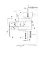
図1は本発明の第1実施形態に係る電流駆動装置が適用されたレーザダイオード装置の全体構成を示す概略回路図である。図1に示すように、本実施形態の電流駆動装置1は、被駆動回路であるレーザダイオード2を駆動する駆動回路11を有している。駆動回路11は、後述する3端子レギュレータからの出力電圧に基づいて駆動電流を生成し、レーザダイオード2を駆動する。レーザダイオード2は、レーザダイオード駆動端子20を介して電流駆動装置1に接続されている。
<First Embodiment>
FIG. 1 is a schematic circuit diagram showing an overall configuration of a laser diode device to which a current driving device according to a first embodiment of the present invention is applied. As shown in FIG. 1, the
電流駆動装置1は、駆動回路11に出力電圧を出力するための3端子レギュレータ構成回路12を有している。3端子レギュレータ構成回路12は、外部のパワートランジスタ3と接続されることにより、3端子レギュレータ10を構成する。このため、電流駆動装置1には、3端子レギュレータ構成回路12への入力端子として、パワートランジスタ3と接続するための主端子接続端子13および制御端子接続端子14を有している。
The
パワートランジスタ3は、例えば電界効果型トランジスタ(FET)等で構成されており、主端子の一方(例えばドレイン端子)に接続された第1の電源(電圧源)4の電圧(例えば12Vの電源電圧)を制御端子(例えばゲート端子)からの入力に基づいて所定の目標出力電圧(例えば8.6V)に降圧するものである。なお、パワートランジスタ3は、FETだけでなく、他のトランジスタ(例えばバイポーラトランジスタ等)でも適用可能である。パワートランジスタ3の主端子の他方(例えばソース端子)は主端子接続端子13に接続されており、パワートランジスタ3の制御端子は制御端子接続端子14に接続されている。また、第1の電源4とパワートランジスタ3の制御端子との間には第1の抵抗素子5が設けられている。
The
3端子レギュレータ構成回路12にパワートランジスタ3が接続されることにより構成される3端子レギュレータ10は、第1の電源4に接続される箇所が入力端子INとして機能し、駆動回路11に接続され、パワートランジスタ3により降圧された出力電圧を出力する箇所が出力端子OUTとして機能し、グランドに接続している箇所がグランド端子GNDとして機能する。本実施形態においては、パワートランジスタ3のソース端子が出力端子OUTに接続されている。
The three-
3端子レギュレータ構成回路12には、主端子接続端子13に接続され、出力電圧を分圧する第1分圧抵抗回路を構成する第5の抵抗素子15および第6の抵抗素子16が設けられている。第5の抵抗素子15と第6の抵抗素子16との接続点には、第1の制御トランジスタ17の制御端子(例えばベース端子)が接続されている。第1の制御トランジスタ17の主端子の一方(例えばコレクタ端子)は、制御端子接続端子14に接続されている。第1の制御トランジスタ17の主端子の他方(例えばエミッタ端子)には、3端子レギュレータ10の目標出力電圧を設定する電圧設定回路18が接続されている。電圧設定回路18は、第1の電源4より低い電圧(例えば5Vの電源電圧)を出力する第2の電源(電圧源)6に接続され、当該第2の電源6から供給される電力を用いて、グランドを基準とする設定電圧VSを第1の制御トランジスタ17の主端子の他方に与える。3端子レギュレータ構成回路12は、電圧設定回路18から出力された設定電圧VSに基づいてパワートランジスタ3の制御端子に目標出力電圧に対応する制御電圧を印加する。換言すると、電圧設定回路18は、3端子レギュレータ構成回路12に設定電圧VSに応じた制御電圧をパワートランジスタ3の制御端子に印加させることにより、3端子レギュレータ10が出力する出力電圧を目標出力電圧に設定する。
The three-terminal
上記構成において、第1の制御トランジスタ17のベース−エミッタ間電圧をVBE1とし、第5の抵抗素子15の抵抗値をR2とし、第6の抵抗素子16の抵抗値をR3とすると、出力端子OUTに印加される出力電圧VOUTは、VOUT=(VBE1+VS)・(R2+R3)/R3となる。このように、パワートランジスタ3および3端子レギュレータ構成回路12で構成される3端子レギュレータ10は、第1の制御トランジスタ17のベース−エミッタ間電圧VBE1と電圧設定回路18の設定電圧VSとの和を、第5の抵抗素子15の抵抗値と第6の抵抗素子16の抵抗値との和に対する第6の抵抗素子16の抵抗値の比率で除した電圧VOUTを出力端子OUTから安定的に出力する。
In the above configuration, when the base-emitter voltage of the
上記構成によれば、主端子接続端子13にパワートランジスタ3の主端子を接続するとともに制御端子接続端子14にパワートランジスタ3の制御端子を接続することにより、3端子レギュレータ10を容易に形成することができる。そして、パワートランジスタ3が電流駆動装置1に接続された状態となることにより、電流駆動装置1に3端子レギュレータ10が組み込まれた構成となり、3端子レギュレータ10が、第1の電源4より低い電圧を出力する第2の電源6の電圧を用いて、目標出力電圧に対応する制御電圧を出力電圧VOUTに基づいて変化させてパワートランジスタ3の制御端子に印加することによって、第1の電源4の電圧をパワートランジスタ3により降圧するとともに当該降圧する電圧を目標出力電圧にフィードバック制御して出力電圧として出力する。
According to the above configuration, the three-
なお、本実施形態においては、3端子レギュレータ10の発振成分を吸収するための位相補償回路として、パワートランジスタ3の主端子の他方と制御端子との間に抵抗素子21およびコンデンサ22が接続されている。
In the present embodiment, a
図2は図1に示される電流駆動装置の電圧設定回路の構成を示す概略回路図である。図2に示すように、本実施形態における電圧設定回路18は、第1の制御トランジスタ17の主端子の他方(例えばエミッタ端子)に接続されるバッファ181と、第2の電源6より供給される電力により所定の定電流を出力する定電流回路182と、定電流回路182とグランドとの間に直列接続され、所定の電圧を設定する複数(図2においては2つ)の電圧設定抵抗回路(第7の抵抗素子183および第8の抵抗素子184)と、定電流回路182から出力される定電流と複数の電圧設定抵抗回路183,184による複数の抵抗値とで生成される複数の電圧をバッファ181に選択的に印加する複数のスイッチ素子185,186とを有している。複数のスイッチ素子185,186は、電流駆動装置1の内部または外部に設けられた制御部(図示せず)からの電圧制御信号に応じて選択的にオン(抵抗素子183,184とバッファ181とを接続)するよう構成されている。複数のスイッチ素子185,186は、例えばFET等のトランジスタ等により構成される種々のスイッチ素子が適用可能である。なお、バッファ181は電流吸い込み能力を有している。
FIG. 2 is a schematic circuit diagram showing the configuration of the voltage setting circuit of the current driver shown in FIG. As shown in FIG. 2, the
上記構成において、バッファ181の入出力間の電圧が同一であり、第1の制御トランジスタ17のベース電流が略0であると仮定した場合を考える。電圧設定回路18の出力電圧である設定電圧VSは、定電流回路182から出力される電流をIaとし、抵抗素子183,184の抵抗値をR8,R9とすると、スイッチ素子185のみオンした場合には、VS=Ia・(R8+R9)となり、スイッチ素子186のみオンした場合には、VS=Ia・R9となる。従って、スイッチ素子185,186の接続を切り替えることにより、3端子レギュレータ構成回路12の出力電圧VOUTの値を2段階に切り替えることができる。なお、電圧設定抵抗回路183,184およびスイッチ素子185,186の数を増やすことにより、より多くの段階に切り替えることができる電流駆動装置1を実現することができる。また、定電流回路と1つの抵抗素子とにより1つの設定電圧VSを生成する構成としてもよい。
Consider a case where it is assumed in the above configuration that the voltage between the input and output of the
ここで、本実施形態における電流駆動装置1は、制御端子接続端子14に接続され、第1の電源4から電力が供給されると、3端子レギュレータ構成回路12の出力電圧VOUTが予め定められた電圧VC以下となるようにパワートランジスタ3の制御端子に印加される制御電圧を維持する電圧制限回路19を有している。
Here, when the
まず、電圧制限回路19がない場合の問題を考える。3端子レギュレータ10の作動時においては、電圧設定回路18が第2の電源6からの電力で駆動されることにより、入力端子INから電圧設定回路18のバッファ181に向けて電流が流れる。従って、パワートランジスタ3の制御端子には、第1の電源4の電源電圧から第1の抵抗素子5の抵抗値R1に基づいて降下した電圧が印加されるため、これに応じた出力電圧VOUTが生成される。
First, consider the problem when the
ところが、電圧設定回路18に第2の電源6からの電力が供給されていない状態で第1の電源4からパワートランジスタ3へ電源電圧(例えば12V)が印加された場合、設定電圧VSを切り替える複数のスイッチ素子185,186がすべてオフされた状態となり電圧設定回路18のバッファ181への電流の吸い込みがなくなる(電圧設定回路18の出力がハイインピーダンス状態となる)。従って、第1の制御トランジスタ17に電圧が印加されず、レギュレータ動作が不能となる。これにより、第1の抵抗素子5に電流が流れなくなる。従って、パワートランジスタ3の制御端子にも第1の電源4の電源電圧(例えば12V)が第1の抵抗素子5で電圧降下することなく印加されることとなるため、駆動回路11の内部構成が出力電圧VOUTに対して電流を要求するような回路(例えば出力端子OUTとグランド端子GNDとの間に抵抗が接続されているような回路等)を有する場合、パワートランジスタ3は飽和領域で動作し、出力端子OUTの出力電圧VOUTは第1の電源4の電圧からパワートランジスタ3のゲート−ソース間電圧(例えば約1V)降下しただけの電圧(例えば約11V)が出力されることとなる。また、駆動回路11の内部構成が出力電圧VOUTに対して電流を要求しない回路であれば、パワートランジスタ3は非飽和領域で動作し、電圧降下はパワートランジスタ3のドレイン−ソース間がオン抵抗成分であると考えられ、出力電圧VOUTは第1の電源4の電圧である約12Vがそのまま出力されることになる。例えば通常約8.6Vで駆動する駆動回路11の耐圧が10Vである場合、駆動回路11に11Vの電圧が印加されると、故障や破損の原因となり問題である。このように、電圧制限回路19がない場合、第1の電源4より第2の電源6を先に投入すると駆動回路11およびレーザダイオード2が故障や破損するおそれが生じる。
However, when a power supply voltage (for example, 12 V) is applied from the
そこで、本実施形態においては、制御端子接続端子14に電圧制限回路19が接続されている。これにより、第1の電源6からの電力供給時においても3端子レギュレータ構成回路12の出力端子VOUTが予め定められた電圧VC(例えば10V)以下となるように制御電圧が維持されるため、3端子レギュレータ構成回路12を制御するための第2の電源6が投入される前に3端子レギュレータ構成回路12の出力電圧VOUTを生成する第1の電源4が投入された場合でも、3端子レギュレータ構成回路12の出力電圧VOUTが駆動回路11の耐圧を超えることを防止することができる。従って、2つの電源4,6の投入順序に拘らず駆動電圧を駆動回路11へ安定的に供給することができる。
Therefore, in this embodiment, the
以上のように、3端子レギュレータ10を電流駆動装置1に組み込む際に問題となる2つの電源の投入順序の問題を電圧制限回路19を設けることにより解決することができるため、3端子レギュレータ10を電流駆動装置1に組み込むことができる。従って、電流駆動装置1において部品点数を少なくすることができる。さらに、3端子レギュレータ10を構成する要素のうち、パワートランジスタ3を外付けとすることにより、電流駆動装置1内で発熱量が増加したり、電流駆動装置1を構成する集積回路面積を小さくすることができる。
As described above, the problem of the turn-on order of the two power supplies, which becomes a problem when the three-
また、上記構成とすることにより、主端子接続端子13、制御端子接続端子14、3端子レギュレータ構成回路12、駆動回路11、電圧設定回路18および電圧制限回路19は、1つの集積回路として構成することができる。これにより、部品点数を少なくするとともに、集積回路の面積を小さくすることができる。
Further, with the above configuration, the main
<第2実施形態>
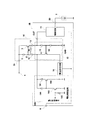
次に、本発明に係る第2実施形態について説明する。図3は本発明の第2実施形態に係る電流駆動装置が適用されたレーザダイオード装置の全体構成を示す概略回路図である。本実施形態において第1実施形態と同様の構成については同じ符号を付し説明を省略する。
Second Embodiment
Next, a second embodiment according to the present invention will be described. FIG. 3 is a schematic circuit diagram showing an overall configuration of a laser diode device to which the current driving device according to the second embodiment of the present invention is applied. In the present embodiment, the same components as those in the first embodiment are denoted by the same reference numerals and description thereof is omitted.
図3に示すように、本実施形態の電流駆動装置1Bが第1実施形態と異なる点は、電圧制限回路19Bが、制御端子接続端子14に一端が接続された第2の抵抗素子191と、主端子の一方(例えばコレクタ端子)が第2の抵抗素子191の他端に接続され、主端子の他方(例えばエミッタ端子)がグランドに接続された第2の制御トランジスタ192と、主端子の一方(例えばドレイン端子)が第3の抵抗素子194を介して制御端子接続端子14に接続され、主端子の他方(例えばソース端子)がグランドに接続され、第2の電源6の電圧が所定電圧以上である場合にオンして第2の制御トランジスタ192の制御端子(例えばベース端子)をグランドに接続させる第3の制御トランジスタ193とを有していることである。本実施形態において、第2の制御トランジスタ192はバイポーラトランジスタで構成されており、第3の制御トランジスタ193はFETで構成されている。
As shown in FIG. 3, the
より詳しくは、第2の抵抗素子191は、一方が制御端子接続端子14を介して第1の抵抗素子5と直列接続され、他方が第2の制御トランジスタ192の主端子の一方(コレクタ端子)に接続されている。これにより、第1の抵抗素子5と第2の抵抗素子191とが第2分圧抵抗回路を構成する。また、第3の制御トランジスタ193の制御端子には第9の抵抗素子195の一端が接続されている。第9の抵抗素子195の他端はグランドに接続されている。第3の制御トランジスタ193の制御端子には、電流駆動装置1の内部または外部に設けられた制御部(図示せず)からの電圧制御信号が入力される。具体的には、駆動回路11の非駆動時には第1の電圧レベルLが第3の制御トランジスタ193の制御端子に入力され、駆動回路11の駆動時には第1の電圧レベルLより高い電圧レベルを有する第2の電圧レベルHが入力される。第3の制御トランジスタ193は、第1の電圧レベルLが入力されるとオフし、第2の電圧レベルHが入力されるとオンする。第3の制御トランジスタ193の制御端子に第2の電圧レベルHが入力されることにより、第2の制御トランジスタ192の制御端子がグランド電位になる。
More specifically, one of the
上記構成において、第2の電源6が投入されていないか第2の電源6が投入されてからパワートランジスタ3の制御が可能な電圧まで立ち上がっていない場合に、第3の制御トランジスタ193の制御端子は、電圧制御信号が入力されない限り、第9の抵抗素子195を通じてグランド電位に保持される。従って、第3の制御トランジスタ193がオフする。そうすると、第2の制御トランジスタ192は、制御端子の電位が第3の抵抗素子194によりプルアップされるとともに第3の抵抗素子194を通じて当該制御端子に電流が流れてオン状態となる。なお、第2の制御トランジスタ192においては、コレクタ−エミッタ間電圧が生じることとなるが、飽和状態(飽和電圧:約200mV)となり、無視し得る略一定の値となる。これにより、パワートランジスタ3の制御端子には、実質的に第1の電源4の電圧が第2分圧抵抗回路で分圧されてなる電圧が印加される。その結果、当該電圧よりパワートランジスタ3の閾値電圧だけ低い電圧が3端子レギュレータ構成回路12の出力電圧VOUTとして出力される。
In the above configuration, the control terminal of the
このように、第2の電源6の電力が供給されていない非駆動時において、第1の電源4の電圧が第2分圧抵抗回路で分圧されるため、予め分圧比(第1の抵抗素子5の抵抗値と第2の抵抗素子191の抵抗値との比)を適宜決定しておくことにより、3端子レギュレータ構成回路12の出力電圧VOUTを所望の(駆動回路11の耐圧より小さい)電圧以下に容易に保持することができる。例えば第1の電源4の電源電圧を12Vとし、分圧比を1:1(例えば第1の抵抗素子5および第2の抵抗素子191の抵抗値をそれぞれ25kΩ)とした場合、パワートランジスタ3の制御端子には、約6Vの電圧が印加されることとなるため、出力端子OUTに印加される電圧は約5Vとなる。
As described above, since the voltage of the
一方、第2の電源6が供給される駆動時においては、第3の制御トランジスタ193に入力される電圧レベルが第2の電圧レベルHとなるため、第2の制御トランジスタ192の制御端子がグランド電位になる。これにより、第2の制御トランジスタ192には電流が流れなくなり、第1実施形態において説明したような通常の3端子レギュレータ構成回路12による出力電圧VOUTの制御(レギュレータ動作)が行われる。なお、このとき第3の制御トランジスタ193がオン状態となるため、第3の抵抗素子194および第3の制御トランジスタ193へ電流が流れることとなる。この電流は3端子レギュレータ構成回路12による出力電圧VOUTの制御において無駄であるため、第3の抵抗素子194の抵抗値を大きくすることで可能な限り第3の抵抗素子194への電流が流れないようにすることが好ましい。
On the other hand, at the time of driving in which the
<第3実施形態>
次に、本発明に係る第3実施形態について説明する。図4は本発明の第3実施形態に係る電流駆動装置が適用されたレーザダイオード装置の全体構成を示す概略回路図である。本実施形態において第1実施形態と同様の構成については同じ符号を付し説明を省略する。
<Third Embodiment>
Next, a third embodiment according to the present invention will be described. FIG. 4 is a schematic circuit diagram showing the overall configuration of a laser diode device to which the current driving device according to the third embodiment of the present invention is applied. In the present embodiment, the same components as those in the first embodiment are denoted by the same reference numerals and description thereof is omitted.
図4に示すように、本実施形態の電流駆動装置1Cが第1実施形態と異なる点は、電圧制限回路19Cが、第1の電源4で動作し、第2の電源6からの電圧を検出する電圧検出回路196と、制御端子接続端子14に一端が接続された第4の抵抗素子197と、主端子の一方(例えばドレイン端子)が第4の抵抗素子197の他端に接続され、主端子の他方(例えばソース端子)がグランドに接続され、制御端子(例えばゲート端子)が電圧検出回路196の出力端子に接続された第4の制御トランジスタ198とを有し、電圧検出回路196が、検出された電圧が所定の閾値電圧未満である場合に第4の制御トランジスタ198をオンさせるよう構成されていることである。本実施形態において、第4の制御トランジスタ198は、FETで構成されている。
As shown in FIG. 4, the
より詳しくは、第4の抵抗素子197は、一方が制御端子接続端子14を介して第1の抵抗素子5と直列接続され、他方が第4の制御トランジスタ198の主端子の一方(ドレイン端子)に接続されている。これにより、第1の抵抗素子5と第4の抵抗素子197とが第3分圧抵抗回路を構成している。電圧検出回路196は、制御端子接続端子14に接続され、第1の電源4からの電力供給により動作する。具体的には、電圧検出回路196は、第2の電源6から出力される電圧が検出されない場合に第1の電源4の電力により第4の制御トランジスタ198の電圧レベルを第1のレベルLからそれより高い第2のレベルHへ切り替えて、第4の抵抗素子197をグランドに接続させる。
More specifically, one of the
図5は図4に示される電流駆動装置の電圧検出回路の構成を示す概略回路図である。図5に示すように、電圧検出回路196は、第2の電源6からの電力から所定の第1電圧を取り出す電圧設定抵抗回路66を構成する第10の抵抗素子61および第11の抵抗素子62と、第1の電源4からの電力から所定の第2電圧を取り出すダイオード63と、ダイオード63に流れる電流を制限する第12の抵抗素子64と、電圧設定抵抗回路66から取り出した第1電圧とダイオード63から取り出した第2電圧とを比較するコンパレータ65とを有している。コンパレータ65は、その出力が第4の制御トランジスタ198の制御端子に入力されるよう接続されており、第2電圧より第1電圧が大きい場合に第1の電圧レベルLを出力し、第2電圧より第1電圧が小さい場合に第2の電圧レベルHを出力するよう構成されている。
FIG. 5 is a schematic circuit diagram showing the configuration of the voltage detection circuit of the current driver shown in FIG. As shown in FIG. 5, the
電圧検出回路196は、制御端子接続端子14を介して第1の電源4から供給される電力により、抵抗素子64およびダイオード63に電流が流れ、ダイオード63に参照電圧となる所定の第2電圧が印加される。本実施形態においては、ダイオード63のカソードがグランドに接続され、アノードがコンパレータ65の非反転入力端子(+側入力端子)に入力されている。従って、ダイオード63のアノードに印加される電圧が第2電圧としてコンパレータ65の非反転入力端子に入力される。また、電圧検出回路196は、第2の電源6から供給される電力により、直列接続された電圧設定抵抗回路66に電流が流れ、電圧設定抵抗回路66で分圧された電圧が第1電圧としてコンパレータ65の反転入力端子(−側入力端子)に入力される。
The
ここで、電圧設定抵抗回路66および抵抗素子64は、第2の電源6から供給される電力が3端子レギュレータ10の動作時の電圧(例えば電源電圧5V)となった場合にコンパレータ65の反転入力端子に入力される第1電圧がコンパレータ65の非反転入力端子に入力される第2電圧より大きくなる(好ましくは十分大きくなる)ような抵抗値に設定される。従って、コンパレータ65は、第1の電源4が投入されている状態で第2の電源6が投入されていないか第2の電源6が投入されてからパワートランジスタ3の制御が可能な電圧まで立ち上がっていない場合、第2の電圧レベルHを出力し、第1の電源4および第2の電源6が投入され、第2の電源6からの電圧がパワートランジスタ3の制御が可能な電圧まで立ち上がっている場合、第1の電圧レベルLを出力する。
Here, the voltage
上記構成において、第2の電源6が投入されていないか第2の電源6が投入されてからパワートランジスタ3の制御が可能な電圧まで立ち上がっていない場合、第4の制御トランジスタ198の制御端子の電圧レベルが第2の電圧レベルHとなるため、第4の制御トランジスタ197がオンし、第1の抵抗素子5、制御端子接続端子14、第4の抵抗素子197および第4の制御トランジスタ198に電流が流れる。これにより、パワートランジスタ3の制御端子には、第1の電源4の電圧が第3分圧抵抗回路で分圧されてなる電圧が印加される。その結果、当該電圧よりパワートランジスタ3の閾値電圧だけ低い電圧が3端子レギュレータ構成回路12の出力電圧VOUTとして出力される。
In the above configuration, when the
このように、第2の電源6が供給されていない非駆動時において、第1の電源4の電圧が第3分圧抵抗回路(第1の抵抗素子5および第4の抵抗素子197)で分圧されるため、予め分圧比(第1の抵抗素子5の抵抗値と第4の抵抗素子197の抵抗値との比)を適宜決定しておくことにより、3端子レギュレータ構成回路12の出力電圧VOUTを所望の(駆動回路11の耐圧より小さい)電圧以下に容易に保持することができる。
As described above, when the
一方、第2の電源6が供給される駆動時においては、電圧検出回路196から第4の制御トランジスタ198に入力される電圧レベルが第1の電圧レベルLとなるため、第4の制御トランジスタ198はオフし、第4の抵抗素子197には電流が流れなくなる。従って、3端子レギュレータ10において第1実施形態において説明したような通常の出力電圧VOUTの制御が行われる。
On the other hand, when driving with the
<第4実施形態>
次に、本発明に係る第4実施形態について説明する。図6は本発明の第4実施形態に係る電流駆動装置が適用されたレーザダイオード装置の全体構成を示す概略回路図である。本実施形態において第1実施形態と同様の構成については同じ符号を付し説明を省略する。
<Fourth embodiment>
Next, a fourth embodiment according to the present invention will be described. FIG. 6 is a schematic circuit diagram showing an overall configuration of a laser diode device to which the current driving device according to the fourth embodiment of the present invention is applied. In the present embodiment, the same components as those in the first embodiment are denoted by the same reference numerals and description thereof is omitted.
図6に示すように、本実施形態の電流駆動装置1Dが第1実施形態と異なる点は、電圧制限回路19Dが、制御端子接続端子14に接続され、パワートランジスタ3の制御端子に印加される制御電圧が所定電圧以上となった場合に、当該制御電圧を当該所定電圧に保持するクランプ回路199を有していることである。
As shown in FIG. 6, the
具体的には、クランプ回路199は例えばツェナーダイオードで構成される。この場合、ツェナーダイオード199のカソードが制御端子接続端子14に接続され、アノードがグランドに接続される。ツェナーダイオード199は、所定の逆方向電圧(降伏電圧)が印加された場合に逆方向電流が急激に流れる素子である。従って、降伏電圧を出力電圧VOUTが駆動回路11の耐圧と同じ電圧となるときのパワートランジスタ3の制御端子に印加される制御電圧以下の値に設定することにより、それ以上の電圧(例えば第1の電源4の電圧12V)が制御端子接続端子14に印加された場合にツェナーダイオード199においてアバランシェ降伏現象が生じ、第1の電源4から第1の抵抗素子5に電流が流れるため、駆動回路11に印加する電圧を駆動回路11の耐圧以下とすることができる。
Specifically, the
このように、本実施形態の構成によれば、第2の電源6の投入の有無に拘わらず、パワートランジスタ3の制御端子に印加される電圧が所定電圧以下に保持される。従って、簡単な構成で、3端子レギュレータ構成回路12の出力電圧を所望の(駆動回路11の耐圧より小さい)電圧以下に容易に保持することができる。
Thus, according to the configuration of the present embodiment, the voltage applied to the control terminal of the
なお、クランプ回路199はツェナーダイオードに限られず、パワートランジスタ3の制御端子の電圧が所定電圧以上となった場合に、当該所定電圧に保持する回路であれば適用可能である。
The
以上、本発明の実施の形態について説明したが、本発明は上記実施の形態に限定されるものではなく、その趣旨を逸脱しない範囲内で種々の改良、変更、修正が可能である。例えば、上記複数の実施形態のうち、2以上の実施形態を組み合わせた構成としてもよい。また、上記実施形態において、複数種類のトランジスタ(FETまたはバイポーラトランジスタ)を組み合せて使用しているが、上記実施形態に記載したような回路動作が実現される限り、各トランジスタにおいてどのようなトランジスタを用いることとしてもよい。 Although the embodiments of the present invention have been described above, the present invention is not limited to the above-described embodiments, and various improvements, changes, and modifications can be made without departing from the spirit of the present invention. For example, it is good also as a structure which combined two or more embodiment among said some embodiment. Further, in the above embodiment, a plurality of types of transistors (FET or bipolar transistor) are used in combination. However, as long as the circuit operation as described in the above embodiment is realized, what kind of transistor is used in each transistor. It may be used.
また、上記実施形態においては、被駆動装置がレーザダイオードである電流駆動装置について説明したが、例えば発光ダイオード(LED)、モータ等の他の被駆動装置を駆動するための電流駆動装置に適用してもよい。さらに、被駆動装置がレーザダイオードである電流駆動装置を光ディスク装置に適用する用途以外の用途、例えばレーザダイオードを用いた通信装置や医療装置に本発明が適用されてもよい。 In the above embodiment, the current driving device in which the driven device is a laser diode has been described. However, the present invention is applied to a current driving device for driving other driven devices such as a light emitting diode (LED) and a motor. May be. Furthermore, the present invention may be applied to uses other than the application in which the current driving device whose driven device is a laser diode is applied to an optical disk device, for example, a communication device or a medical device using a laser diode.
本発明は、駆動回路への駆動電圧を駆動回路へ安定的に供給しつつ、その部品点数を少なくすることが可能な電流駆動装置等として有用である。 INDUSTRIAL APPLICABILITY The present invention is useful as a current drive device that can reduce the number of components while stably supplying a drive voltage to the drive circuit to the drive circuit.
1,1B,1C,1D 電流駆動装置
2 レーザダイオード(被駆動装置)
3 パワートランジスタ
4 第1の電源
5 第1の抵抗素子
6 第2の電源
11 駆動回路
12 3端子レギュレータ構成回路
13 主端子接続端子
14 制御端子接続端子
15 第5の抵抗素子(第1分圧抵抗回路)
16 第6の抵抗素子(第1分圧抵抗回路)
17 第1の制御トランジスタ
18 電圧設定回路
19,19B,19C,19D 電圧制限回路
20 レーザダイオード駆動端子
21 位相補償回路の抵抗素子
22 位相補償回路のコンデンサ
61 第10の抵抗素子
62 第11の抵抗素子
63 ダイオード
64 第12の抵抗素子
66 電圧設定抵抗回路
181 バッファ
182 定電流回路
183 第7の抵抗素子(電圧設定抵抗回路)
184 第8の抵抗素子(電圧設定抵抗回路)
185 第1のスイッチ
186 第2のスイッチ
191 第2の抵抗素子
192 第2の制御トランジスタ
193 第3の制御トランジスタ
194 第3の抵抗素子
195 第9の抵抗素子
196 電圧検出回路
197 第4の抵抗素子
198 第4の制御トランジスタ
199 ツェナーダイオード(クランプ回路)
IN 入力端子
OUT 出力端子
GND グランド端子
1, 1B, 1C, 1D
3
16 Sixth resistive element (first voltage dividing resistor circuit)
17
184 Eighth resistance element (voltage setting resistor circuit)
185
IN input terminal OUT output terminal GND Ground terminal
Claims (7)
前記パワートランジスタの制御端子が接続される制御端子接続端子と、
前記主端子接続端子および前記制御端子接続端子に前記パワートランジスタの前記主端子の他方および前記制御端子がそれぞれ接続された状態で、目標出力電圧に対応する制御電圧を出力電圧に基づいて変化させて前記パワートランジスタの制御端子に印加することによって、前記第1の電源の電圧を前記パワートランジスタにより降圧するとともに当該降圧する電圧を前記目標出力電圧にフィードバック制御して前記出力電圧として出力する3端子レギュレータ構成回路と、
前記出力電圧を用いて被駆動装置を駆動する駆動電流を生成する駆動回路と、
前記第1の電源より低い電圧を出力する第2の電源に接続され、前記第2の電源からの電力を用いて、前記3端子レギュレータ構成回路が前記パワートランジスタの制御端子に印加する前記目標出力電圧に対応する制御電圧を設定する電圧設定回路と、
前記制御端子接続端子に接続され、前記第1の電源から電力が供給されると、前記3端子レギュレータ構成回路の出力電圧が予め定められた電圧以下となるように前記パワートランジスタの制御端子に印加される制御電圧を維持する電圧制限回路と、を備える、電流駆動装置。 A main terminal connection terminal to which one of the main terminals is connected to the first power supply and the other of the main terminals of the power transistor is connected;
A control terminal connection terminal to which a control terminal of the power transistor is connected;
With the other of the main terminals of the power transistor and the control terminal connected to the main terminal connection terminal and the control terminal connection terminal, respectively, a control voltage corresponding to a target output voltage is changed based on an output voltage. A three-terminal regulator that applies the voltage to the control terminal of the power transistor to step down the voltage of the first power supply by the power transistor and feedback-controls the voltage to be reduced to the target output voltage and outputs it as the output voltage A configuration circuit;
A drive circuit for generating a drive current for driving the driven device using the output voltage;
The target output that is connected to a second power source that outputs a voltage lower than that of the first power source, and that the three-terminal regulator component circuit applies to the control terminal of the power transistor using the power from the second power source A voltage setting circuit for setting a control voltage corresponding to the voltage;
When the power is supplied from the first power source connected to the control terminal connection terminal, the output voltage of the three-terminal regulator component circuit is applied to the control terminal of the power transistor so as to be equal to or lower than a predetermined voltage. And a voltage limiting circuit for maintaining the controlled voltage.
前記電圧設定回路は、前記第2の電源からの電力を用いて前記目標出力電圧に対応するグランドを基準とした設定電圧を生成し、当該生成した設定電圧を前記3端子レギュレータ構成回路に与えるよう構成されており、
前記3端子レギュレータ構成回路は、
前記主端子接続端子に一端が接続されるとともに他端がグランドに接続され、前記出力電圧を分圧する第1分圧抵抗回路と、
主端子の一方が前記制御端子接続端子に接続され、主端子の他方に前記電圧設定回路の前記設定電圧が与えられ、制御端子に前記第1分圧抵抗回路で分圧された電圧が印加される第1の制御トランジスタと、を有する、請求項1に記載の電流駆動装置。 The control terminal of the power transistor is connected to the first power supply via a first resistance element,
The voltage setting circuit generates a setting voltage based on the ground corresponding to the target output voltage using the power from the second power supply, and supplies the generated setting voltage to the three-terminal regulator component circuit. Configured,
The three-terminal regulator component circuit is:
A first voltage dividing resistor circuit that has one end connected to the main terminal connecting terminal and the other end connected to the ground, and divides the output voltage;
One of the main terminals is connected to the control terminal connection terminal, the set voltage of the voltage setting circuit is applied to the other of the main terminals, and the voltage divided by the first voltage dividing resistor circuit is applied to the control terminal. The current driving device according to claim 1, further comprising: a first control transistor.
前記制御端子接続端子に一端が接続された第2の抵抗素子と、
主端子の一方が前記第2の抵抗素子の他端に接続され、主端子の他方がグランドに接続された第2の制御トランジスタと、
主端子の一方が第3の抵抗素子を介して前記制御端子接続端子に接続されるとともに前記第2の制御トランジスタの制御端子に接続され、主端子の他方がグランドに接続され、前記第2の電源の電圧が所定電圧以上である場合にオンして前記第2の制御トランジスタの制御端子をグランドに接続させる第3の制御トランジスタと、を有する、請求項2に記載の電流駆動装置。 The voltage limiting circuit is:
A second resistance element having one end connected to the control terminal connection terminal;
A second control transistor having one main terminal connected to the other end of the second resistance element and the other main terminal connected to the ground;
One of the main terminals is connected to the control terminal connection terminal via a third resistance element and connected to the control terminal of the second control transistor, the other of the main terminals is connected to the ground, and the second 3. A current driving device according to claim 2, further comprising: a third control transistor that is turned on when a voltage of a power source is equal to or higher than a predetermined voltage and connects a control terminal of the second control transistor to a ground.
前記第1の電源で動作し、前記第2の電源からの電圧を検出する電圧検出回路と、
前記制御端子接続端子に一端が接続された第4の抵抗素子と、
主端子の一方が前記第4の抵抗素子の他端に接続され、主端子の他方がグランドに接続され、制御端子が前記電圧検出回路の出力端子に接続された第4の制御トランジスタと、を有し、
前記電圧検出回路は、検出された電圧が所定の閾値電圧未満である場合に前記第4の制御トランジスタをオンさせるよう構成されている、請求項2に記載の電流駆動装置。 The voltage limiting circuit is:
A voltage detection circuit that operates on the first power source and detects a voltage from the second power source;
A fourth resistance element having one end connected to the control terminal connection terminal;
A fourth control transistor having one main terminal connected to the other end of the fourth resistance element, the other main terminal connected to the ground, and a control terminal connected to the output terminal of the voltage detection circuit; Have
The current driving device according to claim 2, wherein the voltage detection circuit is configured to turn on the fourth control transistor when the detected voltage is lower than a predetermined threshold voltage.
The current driving device according to claim 1, wherein the driven device is a laser diode, and the driving circuit is a laser current driving circuit that generates a driving current flowing through the laser diode.
Priority Applications (2)
| Application Number | Priority Date | Filing Date | Title |
|---|---|---|---|
| JP2010144661A JP2012009651A (en) | 2010-06-25 | 2010-06-25 | Current driving device |
| US13/167,240 US20110317729A1 (en) | 2010-06-25 | 2011-06-23 | Current driving device |
Applications Claiming Priority (1)
| Application Number | Priority Date | Filing Date | Title |
|---|---|---|---|
| JP2010144661A JP2012009651A (en) | 2010-06-25 | 2010-06-25 | Current driving device |
Publications (1)
| Publication Number | Publication Date |
|---|---|
| JP2012009651A true JP2012009651A (en) | 2012-01-12 |
Family
ID=45352528
Family Applications (1)
| Application Number | Title | Priority Date | Filing Date |
|---|---|---|---|
| JP2010144661A Pending JP2012009651A (en) | 2010-06-25 | 2010-06-25 | Current driving device |
Country Status (2)
| Country | Link |
|---|---|
| US (1) | US20110317729A1 (en) |
| JP (1) | JP2012009651A (en) |
Cited By (1)
| Publication number | Priority date | Publication date | Assignee | Title |
|---|---|---|---|---|
| WO2021181847A1 (en) * | 2020-03-10 | 2021-09-16 | パナソニックIpマネジメント株式会社 | Laser oscillator, and laser processing apparatus comprising same |
Families Citing this family (4)
| Publication number | Priority date | Publication date | Assignee | Title |
|---|---|---|---|---|
| WO2013036370A1 (en) * | 2011-09-11 | 2013-03-14 | Cree, Inc. | High current density power module comprising transistors with improved layout |
| US9373617B2 (en) | 2011-09-11 | 2016-06-21 | Cree, Inc. | High current, low switching loss SiC power module |
| US9640617B2 (en) | 2011-09-11 | 2017-05-02 | Cree, Inc. | High performance power module |
| JP7275984B2 (en) * | 2019-08-09 | 2023-05-18 | オムロン株式会社 | drive circuit |
-
2010
- 2010-06-25 JP JP2010144661A patent/JP2012009651A/en active Pending
-
2011
- 2011-06-23 US US13/167,240 patent/US20110317729A1/en not_active Abandoned
Cited By (1)
| Publication number | Priority date | Publication date | Assignee | Title |
|---|---|---|---|---|
| WO2021181847A1 (en) * | 2020-03-10 | 2021-09-16 | パナソニックIpマネジメント株式会社 | Laser oscillator, and laser processing apparatus comprising same |
Also Published As
| Publication number | Publication date |
|---|---|
| US20110317729A1 (en) | 2011-12-29 |
Similar Documents
| Publication | Publication Date | Title |
|---|---|---|
| JP4658623B2 (en) | Constant current circuit, power supply device and light emitting device using the same | |
| US20170155315A1 (en) | Power Regulator | |
| TWI439022B (en) | Active voltage-clamping gate driver circuit | |
| JP2008147755A (en) | Driving circuit and semiconductor device using the same | |
| KR101069485B1 (en) | Motor drive circuit | |
| JPWO2005096480A1 (en) | Power supply device and display device | |
| JP2007336694A (en) | Drive circuit for insulated-gate semiconductor device | |
| JP2009147515A (en) | Load drive circuit | |
| JP2012009651A (en) | Current driving device | |
| US9531259B2 (en) | Power supply circuit | |
| JP2005086940A (en) | Gate drive circuit | |
| JP2009044304A (en) | Semiconductor element controller | |
| JP5407618B2 (en) | Gate drive circuit and power conversion circuit | |
| US11522535B2 (en) | Semiconductor device | |
| WO2017086028A1 (en) | Step-up/down power supply and power supply circuit | |
| JP2010246294A (en) | Power supply circuit and electronic apparatus | |
| JP6447573B2 (en) | Power supply device and electronic control device | |
| WO2013161201A1 (en) | Driving device | |
| JP4821394B2 (en) | Semiconductor device drive circuit | |
| JP6601372B2 (en) | Gate drive device | |
| JP5009083B2 (en) | Switching power supply circuit | |
| JP5435483B2 (en) | Power supply device | |
| JP6393674B2 (en) | Semiconductor integrated circuit and constant current drive system | |
| JP2015012252A (en) | Current detection circuit | |
| US7859306B2 (en) | Load driving circuit |