JP2012004635A - Temperature variable attenuator - Google Patents
Temperature variable attenuator Download PDFInfo
- Publication number
- JP2012004635A JP2012004635A JP2010135005A JP2010135005A JP2012004635A JP 2012004635 A JP2012004635 A JP 2012004635A JP 2010135005 A JP2010135005 A JP 2010135005A JP 2010135005 A JP2010135005 A JP 2010135005A JP 2012004635 A JP2012004635 A JP 2012004635A
- Authority
- JP
- Japan
- Prior art keywords
- temperature
- temperature variable
- circuit
- pair
- resistor
- Prior art date
- Legal status (The legal status is an assumption and is not a legal conclusion. Google has not performed a legal analysis and makes no representation as to the accuracy of the status listed.)
- Pending
Links
Images


Landscapes
- Attenuators (AREA)
- Non-Reversible Transmitting Devices (AREA)
Abstract
Description
本発明は温度可変減衰器、特に周囲温度に応じて減衰量を変えることができる温度可変減衰器の構成に関する。 The present invention relates to a temperature variable attenuator, and more particularly to a configuration of a temperature variable attenuator capable of changing an attenuation amount according to an ambient temperature.
図10には、従来の温度可変減衰器(下記特許文献1)の構成が示されており、この減衰器では、伝送線路1において使用周波数の略λ/4(λ:使用周波数の波長)の長さの2つの線路(遅延回路)2が設けられ、この2つの線路2のそれぞれを挟む3つの点と接地(GND)との間に、サーミスタ4及び抵抗器5からなる抵抗体(温度可変抵抗体)6が並列に3組配置されている。
FIG. 10 shows a configuration of a conventional temperature variable attenuator (the following Patent Document 1). In this attenuator, the
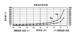
図11には、上記図10の温度可変減衰器の等価回路、図12には、当該減衰器における減衰量対抵抗値の特性が示されており、図11のように、上記抵抗体6はRaとRbの可変抵抗値を持つことになる。このような減衰器(低周波での動作)では、周囲温度が上昇すると、図10の抵抗体6は正温度係数抵抗体であるため、図12に示されるように、抵抗体5の抵抗値Ra及びRbが上昇して減衰量は低下し、反対に周囲温度が下降するときは逆の動作となる。
FIG. 11 shows an equivalent circuit of the temperature variable attenuator shown in FIG. 10, and FIG. 12 shows the characteristics of attenuation versus resistance in the attenuator. As shown in FIG. It has variable resistance values of Ra and Rb. In such an attenuator (operation at a low frequency), when the ambient temperature rises, the
そして、この温度可変減衰器が特性インピーダンスZ0に整合している場合、上記Ra及びRbの抵抗値と減衰量Lとの関係は、図12に示す特性の下、その関係式は次の式に示すようになる。

しかしながら、従来の温度可変減衰器では、第1に、上記サーミスタ4等の温度可変抵抗器が使用されており、この温度可変抵抗器が持つリアクタンス成分により高周波においてV.S.W.R(電圧定在波比)が劣化するという問題がある。
However, in a conventional temperature variable attenuator, first, a temperature variable resistor such as the
図13(A)には、温度可変抵抗器である一般的なチップ型温度可変抵抗器(サーミスタ)の側面断面図が示され、図13(B)にはその等価回路が示されている。図13(A)において、温度可変抵抗器8は、両端の電極9と、この電極9に接続される2つの固定導体板10を有し、この固定導体板10は、常温の抵抗値を調整するために、温度で変化する抵抗体内部に挿入される。従って、2つの固定導体板10の間にコンデンサ成分が生じ、図13(B)に示されるように、温度可変抵抗器の等価回路では、純粋な抵抗Rに並列にリアクタンス成分であるコンデンサCが付加される。
FIG. 13A shows a side sectional view of a general chip-type temperature variable resistor (thermistor) which is a temperature variable resistor, and FIG. 13B shows an equivalent circuit thereof. In FIG. 13A, the
図14には、温度可変抵抗器を用いた場合の高周波での等価回路が示されており、この図14に示されるように、温度可変減衰器でも、抵抗Raに並列にリアクタンス成分Xa、抵抗Rbに並列にリアクタンス成分Xbが付加され、従来の温度可変減衰器においては、このリアクタンス成分Xa,Xbの影響により高周波においてV.S.W.Rが劣化するという問題がある。 FIG. 14 shows an equivalent circuit at a high frequency when a temperature variable resistor is used. As shown in FIG. 14, even in the temperature variable attenuator, a reactance component Xa and a resistor are connected in parallel with the resistor Ra. A reactance component Xb is added in parallel to Rb, and the conventional temperature variable attenuator has a problem that VSWR deteriorates at high frequencies due to the influence of the reactance components Xa and Xb.
図15には、低周波(L−Band帯)における周囲温度と減衰量及びV.S.W.Rとの関係、図16には、高周波(Ku−Band帯)における周囲温度と減衰量及びV.S.W.Rとの関係が示されており、これらの図から分かるように、減衰量については低周波と高周波に大きな差異はないが、回路の整合性の指針であるV.S.W.Rは、低周波(L−Band帯)に比べて高周波(Ku−Band帯)の方が劣化することになる。このV.S.W.Rは、完全に特性インピーダンスと整合されたときは数値1.0であるが、アンプ及びミキサ等の他の回路との接続において好ましいレベルは、一般的に1.2以下である。 FIG. 15 shows the relationship between ambient temperature, attenuation and VSWR in the low frequency (L-Band band), and FIG. 16 shows the relationship between ambient temperature, attenuation and VSWR in the high frequency (Ku-Band band). As can be seen from these figures, although there is no significant difference between the low frequency and the high frequency in terms of attenuation, the VSWR, which is a guideline for circuit matching, has a higher frequency than the low frequency (L-Band band). The (Ku-Band band) will be deteriorated. This V.S.W.R is a numerical value of 1.0 when perfectly matched with the characteristic impedance, but a preferable level in connection with other circuits such as an amplifier and a mixer is generally 1.2 or less.
なお、上記V.S.W.Rを劣化させるコンデンサC成分は温度可変抵抗の定数毎に異なるため、温度可変減衰器の減衰特性を変える目的で温度可変抵抗器の抵抗を変更した際には、上記V.S.W.Rの劣化度も変化し安定した特性を維持することが困難となる。 Since the capacitor C component that degrades the VSWR differs depending on the constant of the temperature variable resistor, when the resistance of the temperature variable resistor is changed for the purpose of changing the attenuation characteristic of the temperature variable attenuator, the degree of deterioration of the VSWR It is difficult to maintain stable characteristics.
第2に、従来の温度可変減衰器に用いられる正温度係数温度可変抵抗器は、負温度係数温度可変抵抗器に比べて常温における抵抗値及び温度変化幅の種類が僅少であり、所望の特性が得られ難いという問題がある。 Secondly, the positive temperature coefficient temperature variable resistor used in the conventional temperature variable attenuator has few kinds of resistance value and temperature change width at room temperature compared with the negative temperature coefficient temperature variable resistor, and has the desired characteristics. There is a problem that it is difficult to obtain.
一般に、温度可変減衰器は、アンプやミキサ等の回路と組み合わせた複合回路において、その複合回路の利得温度変動を緩和するために使用される。そのため、この複合回路が低温になった場合は、図15及び図16の減衰量特性線にも示されるように、温度可変減衰器の減衰量を増加させ、逆に高温に推移した場合には減衰量を低下させる動作が要求される。即ち、図12に示した抵抗値と減衰量との関係から分かるように、従来の温度可変減衰器に使用される温度可変抵抗器8(及び図11の6)は、正温度係数であることが理解できる。 In general, a variable temperature attenuator is used in a composite circuit combined with a circuit such as an amplifier or a mixer in order to reduce gain temperature fluctuation of the composite circuit. Therefore, when this composite circuit becomes low temperature, the attenuation amount of the temperature variable attenuator is increased as shown in the attenuation characteristic lines of FIG. 15 and FIG. An operation for reducing the attenuation is required. That is, as can be seen from the relationship between the resistance value and the attenuation shown in FIG. 12, the temperature variable resistor 8 (and 6 in FIG. 11) used in the conventional temperature variable attenuator has a positive temperature coefficient. Can understand.
しかしながら、実際には正温度係数温度可変抵抗器は、負温度係数温度可変抵抗器に比べて常温における抵抗値及び温度変化幅の種類が僅少であるため、所望の特性が得られ難いという不都合がある。 However, in practice, the positive temperature coefficient temperature variable resistor has a small number of types of resistance values and temperature change ranges at room temperature as compared with the negative temperature coefficient temperature variable resistor, and therefore, it is difficult to obtain desired characteristics. is there.
本発明は上記問題点に鑑みてなされたものであり、その目的は、高周波においても、V.S.W.Rの劣化がなく、入手性の良い負温度係数温度可変抵抗器を用いて所望の特性が容易に得られる温度可変減衰器を提供することにある。 The present invention has been made in view of the above problems, and its object is to achieve V.V. S. W. An object of the present invention is to provide a temperature variable attenuator in which desired characteristics can be easily obtained using a negative temperature coefficient temperature variable resistor which is not easily deteriorated and has good availability.
上記目的を達成するために、請求項1の発明に係る温度可変減衰器は、伝送線路に直列に接続され、使用周波数の略1/4波長の奇数倍の透過位相を有する第1遅延回路と、この第1遅延回路の両端のそれぞれに接続され、使用周波数の略1/4波長の奇数倍の透過位相を有する1対の第2遅延回路と、この1対の第2遅延回路のそれぞれと接地との間に配置され、負温度係数温度可変抵抗器及び固定抵抗器が並列に接続された1対の温度可変抵抗体と、を備え、上記第1遅延回路、1対の第2遅延回路及び1対の温度可変抵抗体にてπ型回路を構成するようにしたことを特徴とする。
請求項2の発明は、上記第1遅延回路、1対の第2遅延回路及び1対の温度可変抵抗体からなるπ型回路を少なくとも2組、伝送線路に直列に接続したことを特徴とする。
In order to achieve the above object, a temperature variable attenuator according to the invention of
The invention of
上記請求項1の構成によれば、温度可変抵抗体により生じるリアクタンス成分がπ型構成の第1遅延回路及び第2遅延回路によって相殺され、高周波においても、特性インピーダンスに対する整合の悪化が僅少となり、V.S.W.Rは良好な値に維持される。また、負温度係数温度可変抵抗器により、低温に推移する場合は減衰量が増加し、逆に高温に推移する場合は減衰量が低下するという動作が維持される。
上記請求項2の構成によれば、2組以上のπ型回路によって、温度可変減衰器において更に良好なV.S.W.R値を得ることができる。
According to the configuration of the first aspect, the reactance component generated by the temperature variable resistor is canceled by the first delay circuit and the second delay circuit having the π-type configuration, and the deterioration of matching with respect to the characteristic impedance is small even at a high frequency. VSWR is maintained at a good value. Further, the negative temperature coefficient temperature variable resistor maintains an operation in which the amount of attenuation increases when the temperature changes to a low temperature and the amount of attenuation decreases when the temperature changes to a high temperature.
According to the configuration of the second aspect, a more favorable VSWR value can be obtained in the temperature variable attenuator by using two or more sets of π-type circuits.
本発明の温度可変減衰器によれば、高周波においても、劣化のない良好なV.S.W.R値が得られ、高周波にも対応できるという効果を奏し、また入手性の良い負温度係数温度可変抵抗器を用いて所望の温度可変特性が容易に得られるという利点がある。 According to the temperature variable attenuator of the present invention, a good V.V. S. W. The R value is obtained, and there is an advantage that it can cope with a high frequency, and there is an advantage that a desired temperature variable characteristic can be easily obtained by using a highly available negative temperature coefficient temperature variable resistor.
図1には、本発明の実施例に係る温度可変減衰器の構成が示されており、図1に示される伝送線路1は、マイクロストリップライン、コプレーナーウェーブガイド等であり、この伝送線路1には、使用周波数の波長をλとすると、略λ/4の長さ(略λ/4の奇数倍の長さ)の線路からなる第1遅延回路(λ/4分布定数線路)14が2つ設けられる。そして、この2つの第1遅延回路14のそれぞれにおいて、その第1遅延回路14の両端に、略λ/4の長さ(略λ/4の奇数倍の長さ)の線路からなる第2遅延回路15が接続され、この第2遅延回路15と接地(GND)との間に、負温度係数のサーミスタ(負温度係数温度可変抵抗器)16及び固定抵抗器5からなる温度可変抵抗体17が接続される。即ち、第1遅延回路14と1対の第2遅延回路15と1対の温度可変抵抗体17にてπ型回路が構成され、実施例では、このπ型回路が2組配置され、また4個の同一特性の負温度係数サーミスタ16が使用されることになる。
FIG. 1 shows a configuration of a variable temperature attenuator according to an embodiment of the present invention. A
図2には、実施例の温度可変減衰器の等価回路が示されており、実施例によれば、λ/4の長さの第1遅延回路14の両端のそれぞれと接地との間に、抵抗値Rとリアクタンス成分Xが並列に存在することになり、このようなπ型回路によって、良好なV.S.W.R値を得ることができる。
FIG. 2 shows an equivalent circuit of the temperature variable attenuator of the embodiment. According to the embodiment, between each of both ends of the
図3には、実施例における低周波であるL−Band帯の周囲温度に対する減衰量及びV.S.W.Rの値、図4には、高周波であるKu−Band帯の周囲温度に対する減衰量及びV.S.W.Rの値が示されており、これらを従来の図15及び図16と比較すると、低周波において、減衰量、V.S.W.Rは共に従来と同様に良好な値が得られ、また高周波においては、V.S.W.R値が1.2以下となり、従来のような悪化がなく、大幅に改善していることが分かる。 FIG. 3 shows attenuation values and VSWR values with respect to the ambient temperature of the L-Band band, which is a low frequency in the embodiment, and FIG. 4 shows attenuation values and VSWR values with respect to the ambient temperature of the Ku-Band band, which is a high frequency. Compared with the conventional FIG. 15 and FIG. 16, the attenuation and VSWR are both good values as in the conventional case at low frequencies, and the VSWR value is 1.2 at high frequencies. It becomes below, and it turns out that there is no deterioration like the past and it is improving significantly.
次に、実施例においてV.S.W.Rが改善する理由を、図5乃至図7により説明する。即ち、図2の等価回路のリアクタンス成分Xに着目すると、V.S.W.Rの悪化をもたらすリアクタンス成分Xは従来回路の場合と同値であるが、図5に示されるように、リアクタンス成分Xは、伝送線路1に設けられたλ/4の第1遅延回路14を介して、接地に対しπ型回路となるように接続され、このπ型回路が2組、直列に配置される形になる。 Next, the reason why V.S.W.R improves in the embodiment will be described with reference to FIGS. That is, paying attention to the reactance component X of the equivalent circuit in FIG. 2, the reactance component X that causes the deterioration of VSWR is the same value as in the conventional circuit, but as shown in FIG. Are connected to the ground so as to form a π-type circuit, and two sets of these π-type circuits are arranged in series.
そして、このπ型回路の1組に着目すると、図6の等価回路のようになるが、この回路において、図のa点〜d点から矢印方向を見たときのインピーダンスは、図7に示されるようになる。図7は、インピーダンスをスミスチャートで示したものであるが、a点で整合状態にあっても、b点では一方のリアクタシス成分Xの影響によって特性インピーダンスに対する整合から逸脱し、更にλ/4の第1遅延回路14により90°位相が回転することによりc点に移行するが、入力端であるd点では、他方のリアクタンス成分Xが上記リアクタンス成分Xの影響を打ち消すように働くことで、概ね特性インピーダンスに対する整合点(V.S.W.R=1.0)となる。
When attention is paid to one set of this π-type circuit, the equivalent circuit of FIG. 6 is obtained. In this circuit, the impedance when the arrow direction is viewed from the points a to d in the figure is shown in FIG. It comes to be. FIG. 7 shows the impedance in a Smith chart. Even if the impedance is in the matching state at point a, the point b deviates from the matching with respect to the characteristic impedance due to the influence of one reactive component X. When the 90 ° phase is rotated by the
実施例では、このようなπ型回路を2組、直列接続することで、温度可変減衰器のリアクタンス成分Xの影響が相殺により解消されることとなり、高周波においても特性インピーダンスに対する整合の悪化が僅少となる。 In the embodiment, by connecting two sets of such π-type circuits in series, the influence of the reactance component X of the temperature variable attenuator is eliminated by cancellation, and the deterioration of the matching with respect to the characteristic impedance is small even at high frequencies. It becomes.
図8には、実施例の温度可変減衰器においてリアクタンス成分Xが相殺された等価回路が示され、図9には、実施例の高周波(Ku−Band帯)での周囲温度に対する抵抗値(R)及び減衰量(L)の値が示されている。図8に示されるように、リアクタンス成分Xの影響が解消された実施例においては、第1遅延回路14の両端のそれぞれと接地との間に、λ/4の第2遅延回路15と温度可変抵抗体17が直列接続されたものとなり、この温度可変抵抗体17の抵抗値Rは、負温度係数サーミスタ16と固定抵抗器5との並列抵抗値となる。
FIG. 8 shows an equivalent circuit in which the reactance component X is canceled in the temperature variable attenuator of the embodiment. FIG. 9 shows a resistance value (R) with respect to the ambient temperature at the high frequency (Ku-Band band) of the embodiment. ) And attenuation (L) values are shown. As shown in FIG. 8, in the embodiment in which the influence of the reactance component X is eliminated, the
そして、上記抵抗値Rと減衰量及びV.S.W.Rとの関係は、次の式3、式4で表わされる。
そして、図9の抵抗値特性線に示されるように、本発明がπ型回路の構成にすることから、上記温度可変抵抗体17の抵抗値Rは、負温度係数(温度上昇に伴って抵抗値が低くなる特性)を持つものとなり、これによって、図9の減衰量特性線のように、温度上昇に伴って減衰量が低下する特性を得ることができる。即ち、上述のように、温度可変減衰器はアンプやミキサ等の回路と組み合わせた複合回路等において利得温度変動を緩和するために使用され、低温になると減衰量を増加させ、逆に高温になると減衰量を低下させる動作が要求されるが、実施例では、π型回路の構成に対応して、負温度係数の温度可変抵抗体17を用いることにより、上記動作を確保することができる。従って、本発明では、このための温度可変抵抗体17として、多くの種類について入手性の高い負温度係数のものを用いることにより、温度可変減衰器において所望の特性を得ることができるという利点がある。
Then, as shown by the resistance value characteristic line of FIG. 9, since the present invention has a π-type circuit configuration, the resistance value R of the
実施例では、π型回路を2組配置したが、このπ型回路は、1組でも、3組以上でもよい。 In the embodiment, two sets of π-type circuits are arranged, but this π-type circuit may be one set or three or more sets.
1…伝送線路、 2…λ/4線路、
4…正温度係数サーミスタ、 5…固定抵抗器、
6,17…温度可変抵抗体、 8…温度可変抵抗器、
9…電極、 10…固定導体板、
14…λ/4の第1遅延回路、15…λ/4の第2遅延回路、
16…負温度係数サーミスタ。
1 ... transmission line, 2 ... λ / 4 line,
4 ... Positive
6, 17 ... temperature variable resistor, 8 ... temperature variable resistor,
9 ... Electrode, 10 ... Fixed conductor plate,
14... Λ / 4 first delay circuit, 15... Λ / 4 second delay circuit,
16 ... Negative temperature coefficient thermistor.
Claims (2)
この第1遅延回路の両端のそれぞれに接続され、使用周波数の略1/4波長の奇数倍の透過位相を有する1対の第2遅延回路と、
この1対の第2遅延回路のそれぞれと接地との間に配置され、負温度係数温度可変抵抗器及び固定抵抗器が並列に接続された1対の温度可変抵抗体と、を備え、
上記第1遅延回路、1対の第2遅延回路及び1対の温度可変抵抗体にてπ型回路を構成するようにした温度可変減衰器。 A first delay circuit connected in series to the transmission line and having a transmission phase that is an odd multiple of approximately ¼ wavelength of the used frequency;
A pair of second delay circuits connected to both ends of the first delay circuit and having a transmission phase that is an odd multiple of approximately ¼ wavelength of the used frequency;
A pair of temperature variable resistors disposed between each of the pair of second delay circuits and the ground and having a negative temperature coefficient temperature variable resistor and a fixed resistor connected in parallel;
A temperature variable attenuator in which a π-type circuit is constituted by the first delay circuit, the pair of second delay circuits, and the pair of temperature variable resistors.
Priority Applications (1)
| Application Number | Priority Date | Filing Date | Title |
|---|---|---|---|
| JP2010135005A JP2012004635A (en) | 2010-06-14 | 2010-06-14 | Temperature variable attenuator |
Applications Claiming Priority (1)
| Application Number | Priority Date | Filing Date | Title |
|---|---|---|---|
| JP2010135005A JP2012004635A (en) | 2010-06-14 | 2010-06-14 | Temperature variable attenuator |
Publications (1)
| Publication Number | Publication Date |
|---|---|
| JP2012004635A true JP2012004635A (en) | 2012-01-05 |
Family
ID=45536174
Family Applications (1)
| Application Number | Title | Priority Date | Filing Date |
|---|---|---|---|
| JP2010135005A Pending JP2012004635A (en) | 2010-06-14 | 2010-06-14 | Temperature variable attenuator |
Country Status (1)
| Country | Link |
|---|---|
| JP (1) | JP2012004635A (en) |
Citations (5)
| Publication number | Priority date | Publication date | Assignee | Title |
|---|---|---|---|---|
| JPH0288303U (en) * | 1988-12-27 | 1990-07-12 | ||
| JPH02260802A (en) * | 1989-03-31 | 1990-10-23 | Nec Corp | Strip line type diode attenuator |
| JPH04159801A (en) * | 1990-10-24 | 1992-06-03 | New Japan Radio Co Ltd | High-frequency attenuator circuit |
| JPH08340226A (en) * | 1995-06-13 | 1996-12-24 | Nec Eng Ltd | Amplifier with rf switch function |
| JP2009200671A (en) * | 2008-02-20 | 2009-09-03 | New Japan Radio Co Ltd | High frequency temperature variable attenuator |
-
2010
- 2010-06-14 JP JP2010135005A patent/JP2012004635A/en active Pending
Patent Citations (5)
| Publication number | Priority date | Publication date | Assignee | Title |
|---|---|---|---|---|
| JPH0288303U (en) * | 1988-12-27 | 1990-07-12 | ||
| JPH02260802A (en) * | 1989-03-31 | 1990-10-23 | Nec Corp | Strip line type diode attenuator |
| JPH04159801A (en) * | 1990-10-24 | 1992-06-03 | New Japan Radio Co Ltd | High-frequency attenuator circuit |
| JPH08340226A (en) * | 1995-06-13 | 1996-12-24 | Nec Eng Ltd | Amplifier with rf switch function |
| JP2009200671A (en) * | 2008-02-20 | 2009-09-03 | New Japan Radio Co Ltd | High frequency temperature variable attenuator |
Similar Documents
| Publication | Publication Date | Title |
|---|---|---|
| KR101757974B1 (en) | Unequal Gysel power divider | |
| US7528677B2 (en) | Temperature compensation attenuator | |
| US12273094B2 (en) | Acoustic wave device, high frequency front end circuit, and communication apparatus | |
| Yu et al. | A radial four-way power divider with the proposed isolation network | |
| JP5155161B2 (en) | Variable capacitance circuit | |
| US9413054B2 (en) | Miniature wideband quadrature hybrid | |
| US20090066443A1 (en) | Signal selecting device | |
| US20090015355A1 (en) | Compensated attenuator | |
| JP2010517462A (en) | RF switch | |
| JP2006191355A (en) | equalizer | |
| RU2553095C1 (en) | Power divider | |
| CA2676680A1 (en) | Rf re-entrant combiner | |
| JP2012004635A (en) | Temperature variable attenuator | |
| JP2016052111A (en) | Impedance converter | |
| JP4541307B2 (en) | High frequency resonator and high frequency oscillator | |
| JP4940166B2 (en) | High frequency temperature attenuator | |
| KR101321555B1 (en) | Directional coupler using artificial transmission line of triangle patch type | |
| US20250062737A1 (en) | Systems and methods for frequency equalization and temperature compensation in radio frequency devices | |
| Choudhury et al. | Bandpass filters using multilayered microstrip structures | |
| JP2003163514A (en) | Electric power distributor | |
| JP2014158125A (en) | Attenuator | |
| JP6945475B2 (en) | Microwave terminator | |
| WO2019159323A1 (en) | Power divider/combiner circuit and power amplification module | |
| JP2011055181A (en) | Temperature variable attenuator | |
| JP3239720B2 (en) | Microwave attenuator |
Legal Events
| Date | Code | Title | Description |
|---|---|---|---|
| A621 | Written request for application examination |
Free format text: JAPANESE INTERMEDIATE CODE: A621 Effective date: 20130401 |
|
| A977 | Report on retrieval |
Free format text: JAPANESE INTERMEDIATE CODE: A971007 Effective date: 20140122 |
|
| A131 | Notification of reasons for refusal |
Free format text: JAPANESE INTERMEDIATE CODE: A131 Effective date: 20140128 |
|
| A02 | Decision of refusal |
Free format text: JAPANESE INTERMEDIATE CODE: A02 Effective date: 20140805 |